EP2988306A1 - Unité de registre à décalage, circuit de commande de grille et dispositif d'affichage - Google Patents
Unité de registre à décalage, circuit de commande de grille et dispositif d'affichage Download PDFInfo
- Publication number
- EP2988306A1 EP2988306A1 EP13863685.7A EP13863685A EP2988306A1 EP 2988306 A1 EP2988306 A1 EP 2988306A1 EP 13863685 A EP13863685 A EP 13863685A EP 2988306 A1 EP2988306 A1 EP 2988306A1
- Authority
- EP
- European Patent Office
- Prior art keywords
- terminal
- electrode
- gate
- shift register
- register unit
- Prior art date
- Legal status (The legal status is an assumption and is not a legal conclusion. Google has not performed a legal analysis and makes no representation as to the accuracy of the status listed.)
- Withdrawn
Links
Images


Classifications
-
- G—PHYSICS
- G09—EDUCATION; CRYPTOGRAPHY; DISPLAY; ADVERTISING; SEALS
- G09G—ARRANGEMENTS OR CIRCUITS FOR CONTROL OF INDICATING DEVICES USING STATIC MEANS TO PRESENT VARIABLE INFORMATION
- G09G3/00—Control arrangements or circuits, of interest only in connection with visual indicators other than cathode-ray tubes
- G09G3/20—Control arrangements or circuits, of interest only in connection with visual indicators other than cathode-ray tubes for presentation of an assembly of a number of characters, e.g. a page, by composing the assembly by combination of individual elements arranged in a matrix no fixed position being assigned to or needed to be assigned to the individual characters or partial characters
- G09G3/34—Control arrangements or circuits, of interest only in connection with visual indicators other than cathode-ray tubes for presentation of an assembly of a number of characters, e.g. a page, by composing the assembly by combination of individual elements arranged in a matrix no fixed position being assigned to or needed to be assigned to the individual characters or partial characters by control of light from an independent source
- G09G3/36—Control arrangements or circuits, of interest only in connection with visual indicators other than cathode-ray tubes for presentation of an assembly of a number of characters, e.g. a page, by composing the assembly by combination of individual elements arranged in a matrix no fixed position being assigned to or needed to be assigned to the individual characters or partial characters by control of light from an independent source using liquid crystals
- G09G3/3611—Control of matrices with row and column drivers
- G09G3/3674—Details of drivers for scan electrodes
- G09G3/3677—Details of drivers for scan electrodes suitable for active matrices only
-
- G—PHYSICS
- G11—INFORMATION STORAGE
- G11C—STATIC STORES
- G11C19/00—Digital stores in which the information is moved stepwise, e.g. shift registers
- G11C19/18—Digital stores in which the information is moved stepwise, e.g. shift registers using capacitors as main elements of the stages
- G11C19/182—Digital stores in which the information is moved stepwise, e.g. shift registers using capacitors as main elements of the stages in combination with semiconductor elements, e.g. bipolar transistors, diodes
- G11C19/184—Digital stores in which the information is moved stepwise, e.g. shift registers using capacitors as main elements of the stages in combination with semiconductor elements, e.g. bipolar transistors, diodes with field-effect transistors, e.g. MOS-FET
-
- G—PHYSICS
- G11—INFORMATION STORAGE
- G11C—STATIC STORES
- G11C19/00—Digital stores in which the information is moved stepwise, e.g. shift registers
- G11C19/28—Digital stores in which the information is moved stepwise, e.g. shift registers using semiconductor elements
-
- G—PHYSICS
- G11—INFORMATION STORAGE
- G11C—STATIC STORES
- G11C19/00—Digital stores in which the information is moved stepwise, e.g. shift registers
- G11C19/28—Digital stores in which the information is moved stepwise, e.g. shift registers using semiconductor elements
- G11C19/287—Organisation of a multiplicity of shift registers
-
- G—PHYSICS
- G09—EDUCATION; CRYPTOGRAPHY; DISPLAY; ADVERTISING; SEALS
- G09G—ARRANGEMENTS OR CIRCUITS FOR CONTROL OF INDICATING DEVICES USING STATIC MEANS TO PRESENT VARIABLE INFORMATION
- G09G2300/00—Aspects of the constitution of display devices
- G09G2300/04—Structural and physical details of display devices
- G09G2300/0404—Matrix technologies
- G09G2300/0408—Integration of the drivers onto the display substrate
-
- G—PHYSICS
- G09—EDUCATION; CRYPTOGRAPHY; DISPLAY; ADVERTISING; SEALS
- G09G—ARRANGEMENTS OR CIRCUITS FOR CONTROL OF INDICATING DEVICES USING STATIC MEANS TO PRESENT VARIABLE INFORMATION
- G09G2310/00—Command of the display device
- G09G2310/02—Addressing, scanning or driving the display screen or processing steps related thereto
- G09G2310/0264—Details of driving circuits
- G09G2310/0286—Details of a shift registers arranged for use in a driving circuit
Definitions
- the present disclosure relates to the technical field of display, and more particularly, to a shift register unit, a gate driving circuit and a display apparatus.
- TFT-LCD Thin Film Transistor-Liquid Crystal Display
- a display device with such structure is generally manufactured by making a gate driving circuit and a source driving circuit on a glass panel with a COF (Chip on Film) process or a COG (Chip on Glass, that is, the chip is fixed on the glass directly) process, however, when a resolution is high, outputs of both the gate driver and the source driver are more and a length of the driving circuit would increase, which is disadvantageous for a bonding process of a module driving circuit.
- COF Chip on Film
- COG Chip on Glass
- GOA Gate Driver on Array
- each stage of shift register unit in order to realize precise controlling to each stage of gate driving signals, it is necessary for each stage of shift register unit to comprise a plurality of functional modules, such as a pulling-up module and a pulling-down module for realizing high-low changes in potentials of gate driving signals, a control module for control a pulling-up state or a pulling-down state and an inputting module for performing a scan or reset function, and each functional module further comprises a plurality of transistors.
- a pulling-up module and a pulling-down module for realizing high-low changes in potentials of gate driving signals
- a control module for control a pulling-up state or a pulling-down state and an inputting module for performing a scan or reset function
- each functional module further comprises a plurality of transistors.
- a shift register unit a gate driving circuit and a display apparatus, which are capable of simplifying a structure of the shift register unit and further reducing the number of use of the transistors.
- a shift register unit comprising:
- a gate driving circuit comprising a plurality of stages of the shift register units described above:
- a display apparatus comprising the gate driving circuit described above.
- the number of function modules in the shift register unit can be reduced effectively, the structure of the shift register unit can be simplified, so that the number of use of the transistors can be further reduced and therefore a thin frame design for the display apparatus is realized while the circuit is ensured to operate stably.
- All of transistors utilized in all embodiments of the present disclosure may be thin film transistors or field effect transistors or any other devices with same characteristics, and because a source and a drain of the transistor utilized herein are symmetrical, there is no difference between the source and the drain.
- a source and a drain of the transistor utilized herein are symmetrical, there is no difference between the source and the drain.
- one electrode therein is referred to as a first electrode while the other electrode is referred to as a second electrode.
- the transistor may be classified as a N-type and a P-type according to its characteristics.
- the each stage of shift register unit may comprise a plurality of N-type transistors and a plurality of P-type transistors at the same time, wherein the first electrode of the transistor may be the source of the transistor, while the second electrode of the transistor may be the drain of the transistor.
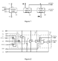
- a shift register unit according to the embodiments of the present disclosure comprises: an inputting module 11, a first outputting module 12 and a second outputting module 13.
- the inputting module 11 is connected with a first signal input terminal INPUT1, a second signal input terminal INPUT2, a first voltage terminal V1, a second voltage terminal V2 and the first outputting module 12, and is configured to control a scan direction of the shift register unit according to a signal inputted from the first signal input terminal INPUT1, a signal inputted from the second signal input terminal INPUT2, a voltage inputted from the first voltage terminal V1 and a voltage inputted from the second voltage terminal V2.
- the first outputting module 12 is connected with a first clock signal terminal CK, a first node A and a first signal output terminal OUTPUT 1, and is configured to control a potential of a signal outputted from the first signal output terminal OUTPUT1 according to a signal inputted from the inputting module 11 and a first clock signal inputted from the first clock signal terminal CK, the first node A is a connection node of the first outputting module 12 and a second outputting module 13.
- the second outputting module 13 is connected with the first node A, a second clock signal terminal CKB and a second signal output terminal OUTPUT2, and is configured to control a potential of a signal outputted from the second signal output terminal OUTPUT2 according to a signal at the first node A and a second clock signal inputted from the second clock signal terminal CKB.
- the number of functional modules in the shift register unit can be reduced effectively, the structure of the shift register unit can be simplified, so that the number of use of the transistors can be further reduced and therefore a thin frame design for the display apparatus is realized while the circuit is ensured to operate stably.
- the inputting module 11 may comprises:
- each transfer gate circuit may function as analog switches for transferring an analog signal, and each transfer gate circuit may comprise a group of N-type transistors and P-type transistors disposed in parallel.
- the transfer gate circuit may further utilize other circuit structure or components having the switching function in the prior art, and the embodiments of the present disclosure are not limited thereto.
- the first transfer gate F1 can comprise:
- the second transfer gate F2 can comprise:
- the inputting module 11 can realize a bi-direction scan of the gate driving circuit, when signals outputted from a previous stage and a next stage of shift register units are used as input signals of the first signal input terminal INPUT1 or the second signal input terminal INPUT2 of the current stage of shift register unit, respectively.
- a signal N-1 OUT outputted from the first signal output terminal OUTPUT 1 of the previous stage of shift register unit can be inputted to the first signal input terminal INPUT1 of the current stage of shift register unit
- a signal N+1 OUT outputted from the first signal output terminal OUTPUT1 of the next stage of shift register unit can be inputted to the second signal input terminal INPUT2 of the current stage of shift register unit.
- the first transistor T1 and the third transistor T3 are the N-type transistors, while the second transistor T2 and the fourth transistor T4 are the P-type transistors.
- the inputting module 11 having such a structure, when a high level VDD is inputted from the first voltage terminal V1 and a low level VSS is inputted from the second voltage terminal V2, a high level outputted from the previous stage of shift register unit can pre-charge the first outputting module 12 through the inputting module 11, and the first outputting module 12 can be reset by a high level outputted from the next stage of shift register unit through the inputting module 11 so as to realize scanning and driving in a direction from up to down in the gate driving circuit.
- the first outputting module 12 can be pre-charged by the high level outputted from the next stage of shift register unit through the inputting module 11, and the first outputting module 12 can be reset by the high level outputted from the previous stage of shift register unit through the inputting module 11, so as to realize scanning and driving in a direction from down to up in the gate driving circuit.
- the signal N+1 OUT outputted from the first signal output terminal OUTPUT1 of the next stage of shift register unit can also be inputted to the first signal input terminal INPUT1 of the current stage of shift register unit, while the signal N-1 OUT outputted from the first signal output terminal OUTPUT1 of the previous stage of shift register unit can also be inputted to the second signal input terminal INPUT2 of the current stage of shift register unit.
- the bi-direction scan of the gate driving circuit can also be realized.
- the bi-direction scan of the gate driving circuit can also be realized by changing the high-low levels of the voltages inputted from the first voltage terminal V1 and the second voltage terminal V2, when the first transistor T1 and the third transistor T3 are the P-type transistors and the second transistor T2 and the fourth transistor T4 are the N-type transistors.
- the first outputting module 12 can comprise:
- each inverter circuit can comprise a pair of N-type transistor and P-type transistor disposed in series.
- the inverter circuit can further utilize other circuit structure or components having the inverting function in the prior art, and the embodiments of the present disclosure are not limited thereto.
- the third voltage terminal V3 can be the high level VDD
- the fourth voltage terminal V4 can be a grounded terminal and the low level VSS.
- the first outputting module 12 can control the potential of the signal outputted from the first signal output terminal OUTPUT1 according to a change in the potential of the signal inputted from the inputting module 11.
- the signal outputted from the first signal output terminal OUTPUT1 can be inputted to the signal input terminal of the previous or next stage of shift register unit, as a start signal or a reset signal to realize the bi-direction scan of the gate driving circuit.
- the first node A and the second node B can be different nodes, and the second node B can be connected to the first signal output terminal OUTPUT1 because a potential at the second node B satisfies the timing of the signal outputted from the first signal output terminal OUTPUT1.
- Such manner is disadvantageous in that the driving ability at the second node B is comparatively low, so it is difficult to drive a large scale circuit and in turn the product quality of the display device is affected.
- the first outputting module 12 can further comprise:
- At least one pair of inverters connected in series which are disposed between the first node A and the second node B.
- the first signal output terminal OUTPUT1 is connected with the first node A. Because the inverter has an effect for improving the driving ability, the driving ability of the signal outputted from the first signal output terminal OUTPUT1 can be improved effectively with the structure comprising the pairs of the inverters connected in series, without changing the phase of the outputted signal.
- the shift register unit illustrated in Fig.2 there is a pair of inverters connected in series between the first node A and the second node B, that is, a second inverter F5 and a third inverter F6.
- the third transfer gate F3 can comprise:
- the first inverter F4 can comprise:
- the second inverter F5 and the third inverter F6 connected in series are disposed between the first node A and the second node B, and the second inverter F5 comprises:
- the third inverter F6 comprises:
- both of the second electrode of the ninth transistor T9 and the second electrode of the tenth transistor T10 are connected with the gate of the eleventh transistor T11 and the gate of the twelfth transistor T12, respectively, to realize the connection of the output terminal of the second inverter F5 with the input terminal of the third inverter F6.
- the first outputting module 12 having such structure can control the potential of the signal outputted from the first signal output terminal OUTPUT1 according to the signal inputted from the inputting module 11 and the clock signal inputted from the first clock signal terminal CK.
- the shift register unit illustrated in Fig.3 is described by taking the transistors T5, T8, T10, T12 being the N-type transistors and the transistors T6, T7, T9, T11 being the P-type transistors as an example. It should be understood that the same functions as the above embodiments can be achieved by changing the third voltage terminal V3, the fourth voltage terminal V4 and the first clock signal terminal CK correspondingly, when the types of the above transistors are changed.
- the second outputting module 13 can comprise:
- the fourth inverter F8 is connected with the NAND gate F7, the third voltage terminal V3 and the fourth voltage terminal V4, respectively, and an output terminal of the fourth inverter F8 is connected with the second signal output terminal OUTPUT2.
- an NAND gate circuit can be composed of a group of AND gate circuits and a group of NOR gate circuits, and both of the AND gate circuit and the NOR gate circuit can comprise a pair of a N-type transistor and a P-type transistor disposed in series.
- the NAND gate circuit can further utilize other circuit structure or components having the NAND function in the prior art, and the embodiments of the present disclosure are not limited thereto.
- the NAND gate F7 can comprise:
- the fourth inverter F8 can comprise:
- the second electrode of the thirteenth transistor T13, the second electrode of the fourteenth transistor T14 and the second electrode of the fifteenth transistor T15 are all connected with the gate of the seventeenth transistor T17 and the gate of the eighteenth transistor T18, respectively, so that it is realized that the output terminal of the NAND gate F7 is connected to the input terminal of the fourth inverter F8.
- the shift register unit illustrated in Fig.3 is described by taking the transistors T14, T16, T18 being the N-type transistors and the transistors T13, T15, T17 being the P-type transistors as an example. It should be understood that the same function as the above embodiments can be achieved by changing the third voltage terminal V3, the fourth voltage terminal V4 and the second clock signal terminal CKB correspondingly, when the types of the above transistors are changed.
- the shift register unit illustrated in Fig.3 there comprise 9 N-type transistors, 9 P-type transistors and one capacitor respectively.
- the number of functional modules in the shift register unit is reduced effectively, the structure of the shift register unit is simplified, and the number of use of the transistors is further reduced, so that difficulties in the circuit design and manufacture are decreased remarkably, and sizes for the circuit area and wiring space are controlled effectively, and therefore a thin frame design for the display apparatus is realized while the circuit is ensured to operate stably.
- the shift register unit adopting such a structure can realize the bi-direction scan of the gate driving circuit by changing the high-low level of the control signals.
- a driving method of the shift register unit, illustrated in Fig.3 according to the embodiments of the present disclosure and its operation states will be described in details below in connection with a signal timing state diagram shown in Fig.4 .
- the manners of pre-charging and resetting can be converted by changing the high-low potentials of the signals STV_N-1, STV_N+1, VDD and VSS, so that the bi-direction scan of the gate driving circuit from up to down or from down to up is realized respectively.
- the number of function modules in the shift register unit can be reduced effectively, the structure of the shift register unit can be simplified, so that the number of use of the transistors can be further reduced and therefore a thin frame design for the display apparatus is realized while the circuit is ensured to operate stably.
- a gate driving circuit comprises a plurality of stages of above shift register units.
- the second signal output terminal OUTPUT2 of each stage of shift register unit SR outputs a line scan signal G for the current stage.
- the first signal output terminal OUTPUT1 of each of the remaining shift register units is connected with a second signal input terminal INPUT2 of the previous stage of shift register unit adjacent thereto; and except for the last stage of shift register unit SRn, the first signal output terminal OUTPUT1 of each of the remaining shift register units is connected with a first signal input terminal INPUT1 of a next stage of shift register unit adjacent thereto.
- a frame start signal STV can be inputted to the first signal input terminal INPUT1 of the first stage of shift register unit SR0; and a reset signal RST can be inputted to the second signal input terminal INPUT2 of the last stage of shift register unit SRn.
- a same data line can be used to provide the frame start signal STV and the reset signal RST to the first stage of shift register unit SR0 and the last stage of shift register unit SRn, respectively.
- the gate driving circuit according to the embodiments of the present disclosure comprises a plurality of shift register units, the number of functional modules in the shift register unit can be reduced effectively, the structure of the shift register unit can be simplified, so that the number of use of the transistors can be further reduced and therefore a thin frame design for the display apparatus is realized while the circuit is ensured to operate stably.
- the inputting module 11 can realize a bi-direction scan of the gate driving circuit. Specifically, a signal N-1 OUT outputted from the first signal output terminal OUTPUT 1 of the previous stage of shift register unit can be inputted to the first signal input terminal INPUT1 of the current stage of shift register unit, and a signal N+1 OUT outputted from the first signal output terminal OUTPUT1 of the next stage of shift register unit can be inputted to the second signal input terminal INPUT2 of the current stage of shift register unit.
- the first transistor T1 and the third transistor T3 are the N-type transistors, while the second transistor T2 and the fourth transistor T4 are the P-type transistors.
- the inputting module 11 having such a structure, when a high level VDD is inputted from the first voltage terminal V1 and a low level VSS is inputted from the second voltage terminal V2, a high level outputted from the previous stage of shift register unit can pre-charge the first outputting module 12 through the inputting module 11, and a high level outputted from the next stage of shift register unit can reset the first outputting module 12 through the inputting module 11, so that the gate driving circuit is realized to scan and drive in a direction from up to down.
- the high level outputted from the next stage of shift register unit can pre-charge the first outputting module 12 through the inputting module 11, and the high level outputted from the previous stage of shift register unit can reset the first outputting module 12 through the inputting module 11, so that the gate driving circuit is realized to scan and drive in a direction from down to up.
- the signal N+1 OUT outputted from the first signal output terminal OUTPUT1 of the next stage of shift register unit can also be inputted to the first signal input terminal INPUT1 of the current stage of shift register unit, while the signal N-1 OUT outputted from the first signal output terminal OUTPUT1 of the previous stage of shift register unit can also be inputted to the second signal input terminal INPUT2 of the current stage of shift register unit.
- the bi-direction scan of the gate driving circuit can also be realized.
- the bi-direction scan of the gate driving circuit can also be realized by changing the high-low levels of the voltages inputted from the first voltage terminal V1 and the second voltage terminal V2, when the first transistor T1 and the third transistor T3 are the P-type transistors and the second transistor T2 and the fourth transistor T4 are the N-type transistors.
- the display apparatus comprises the gate driving circuit including the plurality of the shift register units, the number of function modules in the shift register unit can be reduced effectively, the structure of the shift register unit can be simplified, so that the number of use of the transistors can be further reduced and therefore a thin frame design for the display apparatus is realized while the circuit is ensured to operate stably.
Applications Claiming Priority (2)
| Application Number | Priority Date | Filing Date | Title |
|---|---|---|---|
| CN201310128679.8A CN103208251B (zh) | 2013-04-15 | 2013-04-15 | 一种移位寄存器单元、栅极驱动电路及显示装置 |
| PCT/CN2013/086891 WO2014169626A1 (fr) | 2013-04-15 | 2013-11-11 | Unité de registre à décalage, circuit de commande de grille et dispositif d'affichage |
Publications (2)
| Publication Number | Publication Date |
|---|---|
| EP2988306A1 true EP2988306A1 (fr) | 2016-02-24 |
| EP2988306A4 EP2988306A4 (fr) | 2016-12-28 |
Family
ID=48755463
Family Applications (1)
| Application Number | Title | Priority Date | Filing Date |
|---|---|---|---|
| EP13863685.7A Withdrawn EP2988306A4 (fr) | 2013-04-15 | 2013-11-11 | Unité de registre à décalage, circuit de commande de grille et dispositif d'affichage |
Country Status (4)
| Country | Link |
|---|---|
| US (1) | US9305509B2 (fr) |
| EP (1) | EP2988306A4 (fr) |
| CN (1) | CN103208251B (fr) |
| WO (1) | WO2014169626A1 (fr) |
Families Citing this family (46)
| Publication number | Priority date | Publication date | Assignee | Title |
|---|---|---|---|---|
| CN103208251B (zh) * | 2013-04-15 | 2015-07-29 | 京东方科技集团股份有限公司 | 一种移位寄存器单元、栅极驱动电路及显示装置 |
| JP6245422B2 (ja) * | 2013-07-24 | 2017-12-13 | Tianma Japan株式会社 | 走査回路、及び表示装置 |
| CN103761954B (zh) * | 2014-02-17 | 2016-10-19 | 友达光电(厦门)有限公司 | 显示面板与栅极驱动器 |
| CN103854587B (zh) * | 2014-02-21 | 2017-03-01 | 北京大学深圳研究生院 | 栅极驱动电路及其单元和一种显示器 |
| CN103927982B (zh) * | 2014-03-24 | 2016-08-17 | 京东方科技集团股份有限公司 | 像素电路及其驱动方法、显示装置 |
| CN104036714B (zh) | 2014-05-26 | 2017-02-01 | 京东方科技集团股份有限公司 | Goa电路、显示基板及显示装置 |
| CN104157252B (zh) * | 2014-07-29 | 2017-01-18 | 京东方科技集团股份有限公司 | 一种移位寄存器、栅极驱动电路及显示装置 |
| CN104167195B (zh) * | 2014-08-26 | 2016-08-17 | 昆山龙腾光电有限公司 | 栅极驱动电路单元及其显示面板 |
| CN104318886B (zh) | 2014-10-31 | 2017-04-05 | 京东方科技集团股份有限公司 | 一种goa单元及驱动方法,goa电路和显示装置 |
| CN104464663B (zh) * | 2014-11-03 | 2017-02-15 | 深圳市华星光电技术有限公司 | 低温多晶硅薄膜晶体管goa电路 |
| CN104464817B (zh) * | 2014-12-05 | 2018-06-15 | 深圳市华星光电技术有限公司 | 液晶显示装置及其移位寄存器 |
| US9678593B2 (en) * | 2014-12-31 | 2017-06-13 | Shenzhen China Star Optoelectronics Technology Co. | Gate on array circuit applied to liquid crystal display device |
| CN104485080B (zh) * | 2014-12-31 | 2017-02-22 | 深圳市华星光电技术有限公司 | 用于液晶显示装置的goa电路 |
| CN106033658A (zh) * | 2015-03-18 | 2016-10-19 | 群创光电股份有限公司 | 显示器装置 |
| CN104933982B (zh) | 2015-07-15 | 2017-06-30 | 京东方科技集团股份有限公司 | 移位寄存单元、移位寄存器、栅极驱动电路和显示装置 |
| CN104951142B (zh) * | 2015-07-15 | 2018-04-27 | 厦门天马微电子有限公司 | 一种触控显示面板和显示装置 |
| CN104978922B (zh) * | 2015-07-29 | 2017-07-18 | 京东方科技集团股份有限公司 | 移位寄存器、显示装置及移位寄存器驱动方法 |
| US9824658B2 (en) * | 2015-09-22 | 2017-11-21 | Shenzhen China Star Optoelectronics Technology Co., Ltd | GOA circuit and liquid crystal display device |
| CN105225635B (zh) * | 2015-10-20 | 2018-03-23 | 信利(惠州)智能显示有限公司 | 阵列基板行驱动电路、移位寄存器、阵列基板及显示器 |
| CN105225625B (zh) | 2015-11-05 | 2018-01-23 | 京东方科技集团股份有限公司 | 移位寄存器单元、栅极驱动电路及其驱动方法、显示装置 |
| CN105243995B (zh) * | 2015-11-25 | 2017-09-01 | 上海天马有机发光显示技术有限公司 | 移位寄存器及其驱动方法、栅极驱动电路及其相关器件 |
| CN105427821B (zh) * | 2015-12-25 | 2018-05-01 | 武汉华星光电技术有限公司 | 适用于In Cell型触控显示面板的GOA电路 |
| KR102433746B1 (ko) * | 2015-12-30 | 2022-08-17 | 엘지디스플레이 주식회사 | 게이트 드라이브 ic와 이를 포함한 표시장치 |
| CN105529009B (zh) * | 2016-02-04 | 2018-03-20 | 京东方科技集团股份有限公司 | 移位寄存器及其驱动方法、栅极驱动电路和显示装置 |
| CN105788555B (zh) * | 2016-05-19 | 2018-04-10 | 京东方科技集团股份有限公司 | 移位寄存器单元及其驱动方法、栅极驱动电路、显示装置 |
| US20170358266A1 (en) * | 2016-06-13 | 2017-12-14 | Wuhan China Star Optoelectronics Technology Co., Ltd. | Goa circuit and liquid crystal display |
| CN106023937B (zh) * | 2016-07-28 | 2018-09-18 | 武汉华星光电技术有限公司 | 栅极驱动电路 |
| CN106601190B (zh) * | 2017-03-06 | 2018-12-21 | 京东方科技集团股份有限公司 | 移位寄存器单元及其驱动方法、栅极驱动电路和显示装置 |
| CN106952606B (zh) * | 2017-05-18 | 2020-07-10 | 上海天马有机发光显示技术有限公司 | 一种移位寄存电路单元、移位寄存电路及显示面板 |
| CN107154234B (zh) | 2017-07-20 | 2020-01-21 | 京东方科技集团股份有限公司 | 移位寄存器单元、驱动方法、栅极驱动电路和显示装置 |
| US10311919B2 (en) * | 2017-07-27 | 2019-06-04 | Micron Technology, Inc. | Apparatuses and methods for calibrating sense amplifiers in a semiconductor memory |
| CN107507598A (zh) * | 2017-09-28 | 2017-12-22 | 京东方科技集团股份有限公司 | 一种移位寄存器、栅极驱动电路及显示装置 |
| CN107564459B (zh) * | 2017-10-31 | 2021-01-05 | 合肥京东方光电科技有限公司 | 移位寄存器单元、栅极驱动电路、显示装置及驱动方法 |
| CN107863066A (zh) * | 2017-11-30 | 2018-03-30 | 武汉天马微电子有限公司 | 一种移位寄存器、显示面板、显示装置和驱动方法 |
| CN110299116B (zh) | 2018-03-23 | 2021-01-26 | 京东方科技集团股份有限公司 | 移位寄存器单元及驱动方法、栅极驱动电路、显示装置 |
| KR102575564B1 (ko) * | 2018-03-26 | 2023-09-08 | 삼성디스플레이 주식회사 | 주사 구동부 |
| CN108847185A (zh) * | 2018-06-26 | 2018-11-20 | 昆山国显光电有限公司 | 扫描电路及其驱动方法、显示面板和显示装置 |
| CN109686334B (zh) * | 2019-02-18 | 2021-01-22 | 京东方科技集团股份有限公司 | 栅极驱动电路及其驱动方法、和显示装置 |
| CN109920380B (zh) * | 2019-03-01 | 2020-10-30 | 合肥京东方卓印科技有限公司 | 移位寄存器单元、栅极驱动电路及其控制方法和显示装置 |
| EP3951764A4 (fr) * | 2019-04-02 | 2022-11-09 | BOE Technology Group Co., Ltd. | Unité de registre à décalage et son procédé d'attaque, circuit d'attaque de grille, et appareil d'affichage |
| WO2021056239A1 (fr) * | 2019-09-25 | 2021-04-01 | 京东方科技集团股份有限公司 | Unité de registre à décalage, procédé d'attaque, circuit d'attaque de grille et dispositif d'affichage |
| CN111341261B (zh) * | 2020-04-14 | 2022-06-17 | 合肥京东方显示技术有限公司 | 移位寄存器及其驱动方法、信号驱动电路及显示装置 |
| CN113823640A (zh) | 2020-05-11 | 2021-12-21 | 京东方科技集团股份有限公司 | 显示基板和显示装置 |
| CN112185297B (zh) | 2020-10-26 | 2023-12-05 | 京东方科技集团股份有限公司 | 栅极驱动单元、栅极驱动方法,栅极驱动电路和显示装置 |
| WO2022160086A1 (fr) | 2021-01-26 | 2022-08-04 | 京东方科技集团股份有限公司 | Unité de registre à décalage et son procédé d'attaque, circuit d'attaque de grille, et substrat d'affichage |
| CN113643642B (zh) * | 2021-08-05 | 2022-12-06 | 武汉华星光电技术有限公司 | 栅极驱动电路及显示面板 |
Family Cites Families (12)
| Publication number | Priority date | Publication date | Assignee | Title |
|---|---|---|---|---|
| JP3016354B2 (ja) * | 1996-01-31 | 2000-03-06 | 日本電気株式会社 | マルチプレクサ回路 |
| JP2002132203A (ja) * | 2000-10-25 | 2002-05-09 | Matsushita Electric Ind Co Ltd | パネル駆動用半導体回路装置 |
| JP2003115194A (ja) * | 2001-10-01 | 2003-04-18 | Texas Instr Japan Ltd | シフトレジスタ |
| US6919875B2 (en) * | 2001-10-02 | 2005-07-19 | Rohm Co., Ltd. | Flip-flop circuit, shift register and scan driving circuit for display device |
| KR101319356B1 (ko) * | 2006-06-09 | 2013-10-16 | 엘지디스플레이 주식회사 | 액정표시장치의 쉬프트 레지스터 및 이의 구동방법 |
| KR101243807B1 (ko) * | 2006-06-30 | 2013-03-18 | 엘지디스플레이 주식회사 | 쉬프트 레지스터 |
| JP5358449B2 (ja) * | 2006-11-20 | 2013-12-04 | コピン コーポレーション | 低電力消費用途のためのシフトレジスタ |
| CN101377956B (zh) * | 2007-08-31 | 2010-12-29 | 群康科技(深圳)有限公司 | 移位寄存器及液晶显示器 |
| CN102081969B (zh) * | 2009-12-01 | 2014-06-25 | 群康科技(深圳)有限公司 | 移位寄存电路及双向传输栅极驱动电路 |
| WO2012008186A1 (fr) * | 2010-07-13 | 2012-01-19 | シャープ株式会社 | Registre à décalage et dispositif d'affichage pourvu de ce registre |
| CN102903323B (zh) * | 2012-10-10 | 2015-05-13 | 京东方科技集团股份有限公司 | 移位寄存器单元、栅极驱动电路及显示器件 |
| CN103208251B (zh) * | 2013-04-15 | 2015-07-29 | 京东方科技集团股份有限公司 | 一种移位寄存器单元、栅极驱动电路及显示装置 |
-
2013
- 2013-04-15 CN CN201310128679.8A patent/CN103208251B/zh active Active
- 2013-11-11 EP EP13863685.7A patent/EP2988306A4/fr not_active Withdrawn
- 2013-11-11 WO PCT/CN2013/086891 patent/WO2014169626A1/fr active Application Filing
- 2013-11-11 US US14/368,403 patent/US9305509B2/en active Active
Also Published As
| Publication number | Publication date |
|---|---|
| EP2988306A4 (fr) | 2016-12-28 |
| US20150243237A1 (en) | 2015-08-27 |
| CN103208251A (zh) | 2013-07-17 |
| WO2014169626A1 (fr) | 2014-10-23 |
| US9305509B2 (en) | 2016-04-05 |
| CN103208251B (zh) | 2015-07-29 |
Similar Documents
| Publication | Publication Date | Title |
|---|---|---|
| EP2988306A1 (fr) | Unité de registre à décalage, circuit de commande de grille et dispositif d'affichage | |
| EP3254277B1 (fr) | Unité registre à décalage, pilote de grille et appareil d'affichage associés, et leur procédé de pilotage | |
| US9336898B2 (en) | Shift register unit, gate driver, and display device | |
| EP3499488B1 (fr) | Circuit goa | |
| US10121437B2 (en) | Shift register and method for driving the same, gate driving circuit and display device | |
| US9368230B2 (en) | Shift register unit, gate driving circuit, driving method and display apparatus | |
| CN108932933B (zh) | 移位寄存器、栅极驱动电路、显示装置 | |
| US9196211B2 (en) | Shift register unit, gate driving circuit and display device | |
| CN102708779B (zh) | 移位寄存器及其驱动方法、栅极驱动装置与显示装置 | |
| US9293223B2 (en) | Shift register unit, gate driving circuit and display device | |
| US20170039968A1 (en) | Shift register, gate driving circuit, display apparatus and gate driving method | |
| US20160093264A1 (en) | Shift register unit and gate drive apparatus | |
| KR101310004B1 (ko) | 주사 신호선 구동 회로 및 그것을 구비한 표시 장치 | |
| US9666152B2 (en) | Shift register unit, gate driving circuit and display device | |
| US11282470B2 (en) | Shift register element, method for driving the same, gate driver circuit, and display device | |
| US9201445B2 (en) | Gate driving circuit for thin film transistor liquid crystal display and thin film transistor liquid crystal display | |
| EP3217387A1 (fr) | Unité de registre à décalage, circuit d'attaque de grille et dispositif d'affichage | |
| EP3499495A1 (fr) | Circuit goa | |
| US20180211606A1 (en) | Shift register circuit and driving method therefor, gate line driving circuit and array substrate | |
| US20170025079A1 (en) | Shift register unit and driving method thereof, gate driving circuit and display device | |
| CN100397468C (zh) | 移位寄存电路 | |
| KR20190061081A (ko) | Goa 구동 회로 및 액정 디스플레이 장치 | |
| CN103928001A (zh) | 一种栅极驱动电路和显示装置 | |
| KR20080013280A (ko) | 게이트 구동회로 및 이를 포함하는 표시 장치 | |
| US20210201748A1 (en) | Shift register, driving method thereof, gate driving circuit, and display device |
Legal Events
| Date | Code | Title | Description |
|---|---|---|---|
| PUAI | Public reference made under article 153(3) epc to a published international application that has entered the european phase |
Free format text: ORIGINAL CODE: 0009012 |
|
| 17P | Request for examination filed |
Effective date: 20140624 |
|
| AK | Designated contracting states |
Kind code of ref document: A1 Designated state(s): AL AT BE BG CH CY CZ DE DK EE ES FI FR GB GR HR HU IE IS IT LI LT LU LV MC MK MT NL NO PL PT RO RS SE SI SK SM TR |
|
| AX | Request for extension of the european patent |
Extension state: BA ME |
|
| DAX | Request for extension of the european patent (deleted) | ||
| A4 | Supplementary search report drawn up and despatched |
Effective date: 20161128 |
|
| RIC1 | Information provided on ipc code assigned before grant |
Ipc: G09G 3/00 20060101ALI20161122BHEP Ipc: G11C 19/28 20060101ALI20161122BHEP Ipc: G11C 19/38 20060101AFI20161122BHEP Ipc: G11C 19/18 20060101ALI20161122BHEP Ipc: G09G 3/36 20060101ALI20161122BHEP |
|
| 17Q | First examination report despatched |
Effective date: 20180529 |
|
| STAA | Information on the status of an ep patent application or granted ep patent |
Free format text: STATUS: THE APPLICATION HAS BEEN WITHDRAWN |
|
| 18W | Application withdrawn |
Effective date: 20201105 |