EP2966458A1 - Three-dimensional fine movement device - Google Patents
Three-dimensional fine movement device Download PDFInfo
- Publication number
- EP2966458A1 EP2966458A1 EP15175803.4A EP15175803A EP2966458A1 EP 2966458 A1 EP2966458 A1 EP 2966458A1 EP 15175803 A EP15175803 A EP 15175803A EP 2966458 A1 EP2966458 A1 EP 2966458A1
- Authority
- EP
- European Patent Office
- Prior art keywords
- dimensional
- fine movement
- sample
- unit
- fixed
- Prior art date
- Legal status (The legal status is an assumption and is not a legal conclusion. Google has not performed a legal analysis and makes no representation as to the accuracy of the status listed.)
- Withdrawn
Links
Images


Classifications
-
- G—PHYSICS
- G01—MEASURING; TESTING
- G01Q—SCANNING-PROBE TECHNIQUES OR APPARATUS; APPLICATIONS OF SCANNING-PROBE TECHNIQUES, e.g. SCANNING PROBE MICROSCOPY [SPM]
- G01Q10/00—Scanning or positioning arrangements, i.e. arrangements for actively controlling the movement or position of the probe
- G01Q10/04—Fine scanning or positioning
-
- G—PHYSICS
- G01—MEASURING; TESTING
- G01Q—SCANNING-PROBE TECHNIQUES OR APPARATUS; APPLICATIONS OF SCANNING-PROBE TECHNIQUES, e.g. SCANNING PROBE MICROSCOPY [SPM]
- G01Q70/00—General aspects of SPM probes, their manufacture or their related instrumentation, insofar as they are not specially adapted to a single SPM technique covered by group G01Q60/00
- G01Q70/02—Probe holders
- G01Q70/04—Probe holders with compensation for temperature or vibration induced errors
-
- G—PHYSICS
- G01—MEASURING; TESTING
- G01Q—SCANNING-PROBE TECHNIQUES OR APPARATUS; APPLICATIONS OF SCANNING-PROBE TECHNIQUES, e.g. SCANNING PROBE MICROSCOPY [SPM]
- G01Q10/00—Scanning or positioning arrangements, i.e. arrangements for actively controlling the movement or position of the probe
- G01Q10/02—Coarse scanning or positioning
-
- G—PHYSICS
- G01—MEASURING; TESTING
- G01Q—SCANNING-PROBE TECHNIQUES OR APPARATUS; APPLICATIONS OF SCANNING-PROBE TECHNIQUES, e.g. SCANNING PROBE MICROSCOPY [SPM]
- G01Q20/00—Monitoring the movement or position of the probe
-
- G—PHYSICS
- G01—MEASURING; TESTING
- G01Q—SCANNING-PROBE TECHNIQUES OR APPARATUS; APPLICATIONS OF SCANNING-PROBE TECHNIQUES, e.g. SCANNING PROBE MICROSCOPY [SPM]
- G01Q20/00—Monitoring the movement or position of the probe
- G01Q20/02—Monitoring the movement or position of the probe by optical means
Definitions
- the present invention relates to a three-dimensional fine movement device such as a scanning probe microscope including a mechanism which drives a stage.
- a scanning probe microscope is configured to measure the surface shape of a sample by causing a probe attached to the front end of a cantilever to approach or come into contact with a sample surface.
- a contact mode in which the surface shape of the sample is measured while maintaining an inter-atomic force between the probe and the sample to be constant
- a method (hereinafter, appropriately referred to as a “dynamic force mode (DFM measurement mode)") in which the shape of the sample is measured by using the fact that the amplitude of the probe is attenuated due to intermittent contact between the probe and the sample when the probe approaches the sample by forcibly vibrating the cantilever near a resonance frequency by using a piezoelectric element
- a method hereinafter, appropriately referred to as a “non-contact mode (NC-AFM measurement mode)
- NC-AFM measurement mode non-contact mode
- the scanning probe microscope includes a fine movement unit that includes two (two-axis) fine movement mechanisms (piezoelectric elements) that respectively scan the sample in an xy (plane) direction and one (one-axis) fine movement mechanism (piezoelectric element) that scans the sample in a z (height) direction.
- the sample is mounted on the surface of a stage disposed on the fine movement unit. Since a voltage applied to the piezoelectric element is proportional to the displacement of the piezoelectric element to some extent, height information related to the sample surface may be calculated from the voltage applied to the piezoelectric element. However, since the operational characteristics of the piezoelectric element are hysteresis or creep, it is difficult to obtain an accurate position of the piezoelectric element from the applied voltage.
- the one-axis displacements that are respectively detected for the piezoelectric elements are combined in three directions.
- a piezoelectric element 1100a is slightly displaced on two perpendicular axes (for example, the y direction) as well as a movement direction (x direction)
- a displacement amount in the x direction measured by a position detecting sensor 1100s on the piezoelectric element 1100a is d1
- an actual displacement amount is dx obtained by combining d1 with a fine displacement in the y direction.
- Illustrative aspects of the present invention provide a three-dimensional fine movement device capable of simply and accurately measuring the position of a fixation member or a moving body by directly detecting a three-dimensional position of the fixation member to which the moving body such as a cantilever is fixed by using movement amount detecting means fixed to a coarse movement unit or a base member that relatively does not move in comparison with the fine movement of the moving body.
- a three-dimensional fine movement device comprising: a moving body; a fixation member to which the moving body is fixed; a three-dimensional fine movement unit, to which the fixation member is fixed, and which allows for three-dimensional fine movement of the moving body with the fixation member interposed therebetween; a base member to which the three-dimensional fine movement unit is fixed; and movement amount detecting means that is fixed to the base member and is configured to detect a movement amount of the fixation member.
- the three-dimensional fine movement device by directly detecting the three-dimensional position of the fixation member to which the moving body is fixed by using the movement amount detecting means fixed to the base member that relatively does not move in comparison with the fine movement of the moving body, it is possible to simply and accurately measure the positions of the fixation member and the moving body.
- a three-dimensional fine movement device comprising: a moving body; a fixation member to which the moving body is fixed; a three-dimensional fine movement unit, to which the fixation member is fixed, and which allows for the three-dimensional fine movement of the moving body with the fixation member interposed therebetween; a three-dimensional coarse movement unit, to which the three-dimensional fine movement unit is fixed, and which allows for coarse movement of the three-dimensional fine movement unit on at least one axis of three-dimensional axes at a movement amount greater than that of the three-dimensional fine movement unit; a base member to which the three-dimensional coarse movement unit is fixed; and movement amount detecting means that is fixed to the three-dimensional coarse movement unit and is configured to detect a movement amount of the fixation member.
- the three-dimensional fine movement device by directly detecting the three-dimensional position of the fixation member to which the moving body is fixed by using the movement amount detecting means fixed to the three-dimensional coarse movement unit that relatively does not move in comparison with the fine movement of the moving body, it is possible to simply and accurately measure the positions of the fixation member and the moving body.
- the movement amount detecting means may be configured to detect a detection surface of the fixation member
- the three-dimensional fine movement device by detecting the detection surface by the movement amount detecting means for detecting a diffraction laser beam using, for example, a high-accuracy diffraction grating (volume type hologram grating) as the detection surface, it is possible to more accurately measure the position of the moving body.
- a high-accuracy diffraction grating volume type hologram grating
- a plurality the detection surfaces may be arranged on the respective axes of the three-dimensional axes, and the movement amount detecting means may be provided on the respective detection surface on the respective axes to detect the corresponding detection surfaces.
- the three-dimensional fine movement device by detecting the displacements of the respective three-dimensional axes by the movement amount detecting means, it is possible to more accurately measure the position of the moving body.
- the movement amount detecting means is a non-contact sensor, it is possible to more accurately measure the position of the moving body.
- the non-contact sensor is a sensor that utilizes electrostatic capacitance, optical interference, or optical diffraction, it is possible to more accurately measure the position of the moving body.
- the moving body may be a cantilever that comes into contact with or approaches a sample
- the three-dimensional fine movement device may further comprise a sample stage that is directly fixed to the base member or is fixed to the base member with a three-dimensional coarse movement unit or a second three-dimensional coarse movement unit interposed therebetween, and faces the cantilever, and the sample may be disposed on a surface of the sample stage.
- the second three-dimensional coarse movement unit may move coarsely on an axis that is different from an axis onto which the three-dimensional coarse movement unit moves coarsely.
- the moving body may be a sample
- the three-dimensional fine movement device may further comprise a cantilever attachment unit that is directly or indirectly fixed to the base member, and faces the sample, and a cantilever that comes into contact with or approaches the sample may be disposed on a surface of the cantilever attachment unit.
- the three-dimensional fine movement device may further comprise a control unit configured to perform control on a position on at least one axis of three-dimensional positions of the moving body through closed loop control based on the movement amount detected by the movement amount detecting means.
- the three-dimensional fine movement device it is possible to perform positioning with high accuracy by accurately controlling the three-dimensional position of the moving body or it is possible to measure the position of the moving body while controlling the movement amount.
- the present invention it is possible to simply and accurately measure the position of a fixation member or a moving body by directly detecting a three-dimensional position of the fixation member to which the moving body such as a cantilever is fixed by using movement amount detecting means fixed to a coarse movement unit or a base member that relatively does not move in comparison with the fine movement of the moving body.
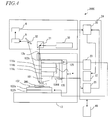
- FIG. 1 is a block diagram of a three-dimensional fine movement device (scanning probe microscope) 200A according to a first illustrative embodiment of the present invention
- FIG. 2 is a cross-sectional view taken along line II-II of FIG. 1 .
- the scanning probe microscope 200A includes a cantilever 1 that holds a probe at the front end thereof, a cantilever attachment unit (inclined block) 101, a cylindrical scanner 111, a base member 13 that forms a frame for supporting the respective components of the scanning probe microscope, a non-contact sensor 130, a detection surface 132 that receives a detection signal from the non-contact sensor 130, a three-dimensional coarse movement unit 122, a sample stage 102 that is disposed on the three-dimensional coarse movement unit 122, a probe microscope controller 24 that controls the entire microscope, and a control unit (computer) 40.
- a control unit computer
- the computer 40 includes a control board for controlling the operation of the scanning probe microscope 200A, a CPU (central processing unit), a ROM, storage means such as a RAM, an interface, and an operation unit.
- a control board for controlling the operation of the scanning probe microscope 200A
- a CPU central processing unit
- ROM read-only memory
- storage means such as a RAM, an interface, and an operation unit.
- the cantilever 1, the cantilever attachment unit 101, the scanner 111, and the non-contact sensor 130 respectively correspond to a "moving body", a “fixation member”, a “three-dimensional coarse movement unit”, and “movement amount detecting means” in the claims.
- the base member 13 has a leftward U shape when viewed from the side, the three-dimensional coarse movement unit 122 is fixed to the upper surface of a lower member of the leftward U-shaped part, and a sample 300 is mounted in a predetermined position of the sample stage 102 disposed on the three-dimensional coarse movement unit 122.
- the scanner 111 is fixed to the lower surface of an upper member of the leftward U-shaped part of the leftward U-shaped base member 13, and the cantilever attachment unit 101 is fixed to the lower surface of the scanner 111.
- the cantilever attachment unit 101 has a substantially square pillar shape of which the front end surface is an inclined surface, and the cantilever 1 is attached to the front end surface in a cantilevered manner.
- the cantilever 1 faces the sample 300, and the probe of the front end of the cantilever 1 comes into contact with or approaches the sample 300, and the surface shape or the surface characteristic of the sample 300 is detected.
- a laser beam is applied from a laser beam source 30 disposed above the base member 13, and the laser beam is applied to the rear surface of the cantilever 1 downward from an irradiation hole 13h penetrating the upper member of the base member 13 through a dichroic mirror 31.
- the laser beam reflected from the cantilever 1 is reflected from a mirror 32, and is detected by a displacement detector 5.
- the movement amount of the cantilever 1 in the vertical direction (z direction) is reflected on a change (incident position) of the optical path of the laser beam incident on the dichroic mirror 31. Accordingly, the displacement amount of the cantilever 1 from the incident position is detected by the displacement detector 5.
- the scanning probe microscope 200A adopts an optical lever type in which a positional deviation of the reflection light of the light incident on the cantilever 1 is detected as a displacement of the cantilever 1 (probe).
- the scanning probe microscope 200A is a scanning probe microscope of a lever type scanning type of performing measurement by scanning the cantilever attachment unit 101 to which the cantilever 1 is attached.
- the probe microscope controller 24 includes a Z control circuit 20, a fine movement control circuit (X, Y, and Z output amplifiers) 22, a coarse movement control circuit 23, and a sensor controller 25, to be described below.
- the probe microscope controller 24 is capable of performing high-speed communication of data by being connected to the computer 40.
- the computer 40 controls the operation condition of a circuit within the probe microscope controller 24, performs input control of measured data, and realizes surface shape measurement, surface property measurement, frequency and vibration characteristics, and force curve measurement.
- the scanner 111 causes the cantilever attachment unit 101 (and the cantilever 1) to three-dimensionally move (fine movement), and is a three-axis piezoelectric element that includes two (two-axis) piezoelectric elements 111a and 111b that scan the cantilever attachment unit 101 in an xy (plane of the sample 300) direction, and a piezoelectric element 111c that scans the cantilever attachment unit 101 in a z (height) direction.
- the piezoelectric element is a sensor in which a crystal is deformed when an electric field is applied and an electric field is generated when the crystal is forcibly deformed due to an external force.
- the piezoelectric element may be generally made of lead zirconate titante (PZT) which is a kind of ceramics, but the material of the piezoelectric element is not limited thereto.
- the piezoelectric elements 111a to 111c are connected to the fine movement control circuit 22, and predetermined control signals (voltages) are output to the fine movement control circuit 22.
- the piezoelectric elements 111a and 111b are driven in the xy direction, and the piezoelectric element 111c is driven in the z direction.
- the three-dimensional coarse movement unit 122 causes the sample 300 to approach the cantilever 1 by coarsely three-dimensionally moving the sample stage 102, and includes an x stage 122a, a y stage 122b, and a z stage 122c.
- the three-dimensional rough movement unit 122 is operated by driving a screw mechanism by a step motor, and is controlled by the rough movement control circuit 23.
- the cantilever attachment unit 101 has a substantially square pillar of which the front end surface is an inclined surface.
- the non-contact sensor 130 includes three non-contact sensors 130a to 130c, and the non-contact sensor 130a faces the cantilever attachment unit 101 from the rear surface (base member 13) of the cantilever attachment unit 101, and the non-contact sensors 130b and 130c face the cantilever attachment unit 101 from both side surfaces (paper surface direction of FIG. 1 ) of the cantilever attachment unit 101.
- detection surfaces 132a to 132c are respectively provided on the three surfaces of the cantilever attachment unit 101 that respectively face the non-contact sensors 130a to 130c.
- the non-contact sensor 130a is attached to the front end of a stay 135a which is attached to the inner surface of a member that vertically extends in the leftward U-shaped part of the base member 13 and extends in the horizontal direction.
- the non-contact sensors 130b and 130c are attached to the front ends of stays 135b and 135c which are attached to the upper surface of the base member 13 and extend downward.
- the detection surfaces 132a to 132c are diffraction gratings (volume type hologram gratings), and the non-contact sensors 130a to 130c are the corresponding laser displacement meters, and the detection surfaces 132a to 132c constitute a part of the "movement amount detecting means".
- the laser displacement meter includes a photo detector that detects the laser beam diffracted by the volume type hologram grating, a polarized light beam splitter that splits the laser beam into S-polarized light and P-polarized light, and a mirror.
- the interference state of the laser beam is changed when the volume type hologram grating moves in one direction (one axis), and interfered light is contrasted according to one pitch of the grating. The displacement on one axis is detected.
- the displacements of the cantilever attachment unit 101 in the x, y and z directions are detected by the non-contact sensors 130a to 130c, as will be described below.
- the three-dimensional coarse movement unit 122 is operated, and the sample 300 approaches the cantilever 1 (probe) by coarsely three-dimensionally moving the sample stage 102.
- the positional relationship between the cantilever 1 and the sample 300 is adjusted by appropriately moving the scanner 111 in the xy direction, and an arbitrary location of the sample 300 is measured.
- the cantilever 1 is sent up to a position that comes into contact with the sample 300 in the z direction by the piezoelectric element 111c of the scanner 111.
- the scanner 111 scans the surface (xy) of the sample 300 while maintaining the displacement amount of the cantilever 1 in the height (z) direction to be constant.
- the property of the surface of the sample 300 is measured using a control signal for maintaining the displacement amount of the cantilever 1 to be constant, as property information.
- the amplitude of the electrical signal of the displacement detector 5 is converted into a direct current level signal by an AC-DC conversion mechanism 6, and is input to the Z control circuit 20.
- the Z control circuit 20 transmits the control signal to a z signal unit of the fine movement control circuit 22, such that the displacement amount of the cantilever 1 in the height (z) direction is maintained to be constant, and the z signal unit outputs a control signal (voltage) for driving the piezoelectric element 111c in the z direction.
- the displacement of the cantilever 1 in the height direction (z) caused by an inter-atomic force acting between the sample 300 and the probe is detected by the aforementioned mechanism, and the piezoelectric element 111c is displaced such that the detected displacement becomes constant.
- the piezoelectric elements 111a and 111b are displaced in the xy direction by the fine movement control circuit 22 to scan the sample 300, and the property or shape of the surface is mapped.
- the three-dimensional position of the cantilever attachment unit 101 is directly detected by the non-contact sensors 130a to 130c.
- the detection signals of the non-contact sensors 130a to 130c are sequentially obtained by the control unit 40 through the sensor controller 25, as an actual three-dimensional displacement amount when the shape or property of the surface is mapped. Based on the detection signals (information) obtained by the control unit 40, the three-dimensional shape of the sample surface is reconfigured.
- the data such as the three-dimensional shape has higher accuracy without interference in the other direction than the three-dimensional displacement amount obtained based on the voltages applied to the piezoelectric elements 111a, 111b and 111c by the scanning probe microscope of the related art.
- the position of the cantilever 1 which is fixed to the cantilever attachment unit 101 and the position of the sample 300 that faces the cantilever 1 to come into contact with or approach the cantilever 1 can be accurately measured, positioning accuracy when the sample 300 is scanned by the cantilever 1 and measurement accuracy or resolution of the shape or property of the surface of the sample 300 are improved.
- the movement (position) on the XY plane is achieved by adopting closed loop control based on the detection signals of the non-contact sensors 130a to 130c, and the movement while performing higher-accuracy positioning can be performed. Thus, it is possible to perform control of a small error in the positioning on the XY plane.
- the closed loop control may not be performed. However, when it is necessary to control the movement amount in the Z direction as in the force curve measurement, the closed loop control based on the detection signal of the non-contact sensor 130c in the Z direction may be performed.
- the closed loop control may be performed by the probe microscope controller 24 and the control unit 40.
- the closed loop control is known feedback control in which data related to the detection signal is fed back to the control unit 40.
- the detection surfaces 132a to 132c are arranged on the respective three-dimensional axes, and the non-contact sensors 130a to 130c are provided for the detection surfaces 132a to 132c of the respective axes to detect the corresponding detection surfaces.
- the three-dimensional position of the cantilever attachment unit 101 at which the detection surfaces 132a to 132c are provided can be more accurately measured.
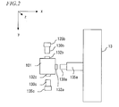
- FIG. 3 is a block diagram of a scanning probe microscope 200B according to a second illustrative embodiment of the present invention.
- the scanning probe microscope 200B is the same as the scanning probe microscope 200A according to the first illustrative embodiment except for the fact that the three-dimensional coarse movement unit 122 is provided between the scanner 111 and the base member 13, the sample stage 102 is directly fixed to the upper surface of the lower member of the leftward U-shaped part of the base member 13, and the attachment structure of the non-contact sensor 130d is different.
- the same components will be assigned the same reference numerals, and the description thereof will be omitted.
- a coarse movement stage 125 is disposed between the three-dimensional coarse movement unit 122 and the scanner 111, and the coarse movement stage 125 is three-dimensionally displaced by the coarse movement of the three-dimensional coarse movement unit 122.
- the scanner 111 is fixed to a part of the lower surface of the coarse movement stage 125, and a stay 136 that extends downward is fixed to the surface of the coarse movement stage 125 to which the scanner 111 is not fixed.
- the non-contact sensor 130d facing the rear surface of the cantilever attachment unit 101 is attached to the front end of the stay 136.
- non-contact sensor 130d only one non-contact sensor 130d is provided, and detects the displacement of the cantilever attachment unit 101 in the z direction.
- the non-contact sensor 130d is an electrostatic capacitance sensor, and the rear surface thereof is the detection surface since it is not necessary to provide the diffraction grating of the first illustrative embodiment as the detection surface on one surface (rear surface) of the cantilever attachment unit 101 facing the non-contact sensor 130d.
- the sample 300 mounted on the three-dimensional coarse movement unit 122 is heavy, a three-dimensional coarse movement position tends to drift significantly due to the weight of the sample 300.
- the influence of the drifting is suppressed, and thus, it is possible to perform the three-dimensional coarse movement.
- all three axes (the x stage 122a, the y stage 122b, and the z stage 122c) of the three-dimensional coarse movement unit 122 are attached to the cantilever attachment unit 101.
- at least one axis of the three axes of the three-dimensional coarse movement unit 122 may be attached to the cantilever attachment unit 101.
- at least the z axis (z stage 122c) is preferably attached to the cantilever attachment unit 101.
- the two axes (the x stage 122a and the y stage 122b) of the three-dimensional coarse movement unit 122 are disposed between the sample stage 102 and the base member 13.
- the two axes (the x stage 122a and the y stage 122b) of the three-dimensional coarse movement unit 122 correspond to a "second three-dimensional coarse movement unit" in the claims.
- the non-contact sensor 130a when the three-dimensional coarse movement unit 122 is fixed to the base member 13 as in the second illustrative embodiment, if the non-contact sensor 130a is fixed to the base member 13, it is necessary to detect the position of the cantilever attachment unit 101 on the scanner 111 that is greatly displaced by the three-dimensional coarse movement unit 122. In this case, the position thereof exceeds the measurement range of the non-contact sensor 130a, and thus, it is difficult to detect the position thereof.
- fixing the non-contact sensor 130a to the three-dimensional coarse movement unit 122 it is possible to accurately detect the displacement amount of the fine movement of the scanner 111 fixed to the three-dimensional coarse movement unit 122 without the influence of the displacement due to the three-dimensional coarse movement.
- the positioning accuracy when the sample 300 is scanned by the cantilever 1 and the measurement accuracy or resolution of the shape or property of the surface of the sample 300 are improved.
- FIG. 5 is a block diagram of a scanning probe microscope 200D according to a third illustrative embodiment of the present invention.
- the scanning probe microscope 200D is the same as the scanning probe microscope 200A according to the first illustrative embodiment except for the fact that the scanner 111 is disposed between the sample stage 102 and the base member 13 and the attachment structure of the non-contact sensor 130a is different.
- the same components will be assigned the same reference numerals, and the description thereof will be omitted.
- the scanning probe microscope 200D is a scanning probe microscope of a sample scanning type that performs the measurement by scanning the sample stage 102 onto which the sample 300 is mounted.
- the non-contact sensor 130a facing the rear surface of the sample stage 102 is attached to the inner surface of the member of the leftward U-shaped part of the base member 13 that extends in the vertical direction.
- the non-contact sensor 130a is configured to detect the displacement of the sample stage 102 in the z direction.
- the non-contact sensor 130a is the same laser displacement meter as that of the first illustrative embodiment, and the detection surface 132a including the diffraction grating is provided on one surface (rear surface) of the sample stage 102 facing the non-contact sensor 130a.
- the sample 300 and the sample stage 102 respectively correspond to a "moving body” and a “fixation member” in the claims.
- the scanning probe microscope 200D is the same optical lever type as that of the first illustrative embodiment, and scans the surface (xy) of the sample 300 while maintaining the displacement amount of the cantilever 1 in the height (z) direction by detecting the displacement of the cantilever 1 (probe) and controlling the height of the sample stage 102 by operating the scanner 111.
- the present invention is not limited to the aforementioned illustrative embodiments.
- the moving body is not limited to the cantilever or the sample, and may include, for example, a probe (indenter) terminal used for an IC test, cutting tools (a drill of a drill press, built-in test equipment (BITE) on a lathe, an end mill of a milling machine, and a cutter on an NC lathe) in precise machining, or a pipette used in a patch clamp system (manipulator).
- a probe indenter
- cutting tools a drill of a drill press, built-in test equipment (BITE) on a lathe, an end mill of a milling machine, and a cutter on an NC lathe
- BITE built-in test equipment
- the measured value is not accurate. Since the thickness of a pipette has a thin diameter of about 10 ⁇ m or is a disposable type that is replaced after use, even if it is attempted to directly measure the position thereof by the sensor, since it is necessary to adjust the initial position of the sensor whenever the pipette is replaced, the pipette is difficult to be measured. As stated above, by measuring the fixation member to which the moving body is fixed, it is possible to avoid the aforementioned problems.
- the movement amount detecting means is not limited to the aforementioned means, and may be a sensor that uses electrostatic capacitance, optical interference or optical diffraction, an optical sensor including an optical fiber and an optical interferometer, or an electrical sensor such as a strain gauge.
- the sensor that uses the electrostatic capacitance, the optical interference or the diffraction grating is preferably used due to high detection accuracy.
- the non-contact sensor 130 is not particularly limited.
- Any movement amount detecting means may be used as long as it can detect the movement amount of the fixation member in at least the one direction (one axis).
- the three-dimensional shaped image is measured from the height displacement of the sample by maintaining the displacement amount between the sample and the cantilever in the height (z) direction to be constant.
- a phase image from the phase value in the resonance state (iii) an error signal image due to a difference with respect to a target value of the vibration amplitude, and (iv) a multi-functional measurement image from the property between the probe and the sample may be measured.
- frequency and vibration characteristics may be measured.
Applications Claiming Priority (1)
| Application Number | Priority Date | Filing Date | Title |
|---|---|---|---|
| JP2014141057A JP2016017862A (ja) | 2014-07-09 | 2014-07-09 | 3次元微動装置 |
Publications (1)
| Publication Number | Publication Date |
|---|---|
| EP2966458A1 true EP2966458A1 (en) | 2016-01-13 |
Family
ID=53717880
Family Applications (1)
| Application Number | Title | Priority Date | Filing Date |
|---|---|---|---|
| EP15175803.4A Withdrawn EP2966458A1 (en) | 2014-07-09 | 2015-07-08 | Three-dimensional fine movement device |
Country Status (4)
| Country | Link |
|---|---|
| US (1) | US10161958B2 (ja) |
| EP (1) | EP2966458A1 (ja) |
| JP (1) | JP2016017862A (ja) |
| CN (1) | CN105320152B (ja) |
Families Citing this family (4)
| Publication number | Priority date | Publication date | Assignee | Title |
|---|---|---|---|---|
| CN108139428A (zh) * | 2015-10-13 | 2018-06-08 | 三思派科有限公司 | 用于实时测试控制的集成测量和微机械定位的设备 |
| KR101787431B1 (ko) * | 2015-12-31 | 2017-10-19 | 한국표준과학연구원 | 변위전달용 선형구조물 및 이를 이용한 1차원 및 3차원 미세 이동 장치 |
| US20190064211A1 (en) * | 2017-08-31 | 2019-02-28 | Oxford Instruments Asylum Research, Inc. | Scanning probe microscope |
| CN112255754A (zh) * | 2020-10-16 | 2021-01-22 | 北京半导体专用设备研究所(中国电子科技集团公司第四十五研究所) | 一种光学镜头对位机构 |
Citations (5)
| Publication number | Priority date | Publication date | Assignee | Title |
|---|---|---|---|---|
| JPH0688724A (ja) * | 1992-09-08 | 1994-03-29 | Canon Inc | 走査型プローブ顕微鏡、メモリー装置及びリソグラフィー装置 |
| JPH06174460A (ja) * | 1992-12-09 | 1994-06-24 | Olympus Optical Co Ltd | スキャナシステム |
| WO2002073125A1 (en) * | 2001-03-09 | 2002-09-19 | Veeco Instruments, Inc. | Apparatus and method for isolating and measuring movement in a metrology apparatus |
| JP2009225654A (ja) | 2008-03-18 | 2009-10-01 | Silicon Touch Technology Inc | 位置検出機能を備えたピエゾアクチュエータシステム及びその方法 |
| US20110203020A1 (en) * | 2010-02-17 | 2011-08-18 | Samsung Electronics Co., Ltd. | Atomic force microscopes and methods of measuring specimens using the same |
Family Cites Families (27)
| Publication number | Priority date | Publication date | Assignee | Title |
|---|---|---|---|---|
| US5025658A (en) * | 1989-11-28 | 1991-06-25 | Digital Instruments, Inc. | Compact atomic force microscope |
| JP3069609B2 (ja) * | 1990-04-17 | 2000-07-24 | セイコーインスツルメンツ株式会社 | 原子間力顕微鏡 |
| JPH0666509A (ja) * | 1992-08-17 | 1994-03-08 | Hitachi Constr Mach Co Ltd | 形状測定装置 |
| US5388452A (en) * | 1993-10-15 | 1995-02-14 | Quesant Instrument Corporation | Detection system for atomic force microscopes |
| JPH08254540A (ja) * | 1995-03-16 | 1996-10-01 | Hitachi Constr Mach Co Ltd | 走査型プローブ顕微鏡 |
| JPH10213587A (ja) * | 1997-01-29 | 1998-08-11 | Olympus Optical Co Ltd | 走査型プローブ顕微鏡 |
| JP3563247B2 (ja) * | 1997-10-31 | 2004-09-08 | 日立建機株式会社 | 走査型プローブ顕微鏡 |
| JPH11211732A (ja) * | 1998-01-27 | 1999-08-06 | Hitachi Constr Mach Co Ltd | 走査型プローブ顕微鏡 |
| JP2001188035A (ja) | 1999-03-17 | 2001-07-10 | Seiko Instruments Inc | 走査型プローブ顕微鏡 |
| JP4155668B2 (ja) * | 1999-05-17 | 2008-09-24 | 日本分光株式会社 | 距離計 |
| JP2001135561A (ja) * | 1999-11-05 | 2001-05-18 | Canon Inc | ステージ装置、露光装置およびデバイス製造方法 |
| JP2005037205A (ja) * | 2003-07-18 | 2005-02-10 | Hitachi Kenki Fine Tech Co Ltd | 走査型プローブ顕微鏡およびその計測方法 |
| JP2005069972A (ja) * | 2003-08-27 | 2005-03-17 | Hitachi Kenki Fine Tech Co Ltd | 走査型プローブ顕微鏡の探針移動制御方法 |
| CN1303396C (zh) * | 2003-11-28 | 2007-03-07 | 天津大学 | 基于显微干涉技术的微机电系统的测试装置与方法 |
| CN1253285C (zh) * | 2004-02-27 | 2006-04-26 | 哈尔滨工业大学 | 微机械零件三维加工装置 |
| WO2006019130A1 (ja) * | 2004-08-18 | 2006-02-23 | Hitachi Kenki Fine Tech Co., Ltd | 走査型プローブ顕微鏡の探針走査制御方法および探針走査制御装置 |
| JP2006118867A (ja) * | 2004-10-19 | 2006-05-11 | Hitachi Kenki Fine Tech Co Ltd | 走査型プローブ顕微鏡及びそれを用いた計測方法 |
| JP2006234507A (ja) * | 2005-02-23 | 2006-09-07 | Hitachi Constr Mach Co Ltd | 走査型プローブ顕微鏡とその測定方法 |
| US20070103697A1 (en) * | 2005-06-17 | 2007-05-10 | Degertekin Fahrettin L | Integrated displacement sensors for probe microscopy and force spectroscopy |
| JP2008002991A (ja) * | 2006-06-23 | 2008-01-10 | Sii Nanotechnology Inc | 微動素子及び走査型プローブ顕微鏡 |
| CN100470378C (zh) * | 2007-04-27 | 2009-03-18 | 清华大学 | 一种超薄3自由度微动工作台 |
| JP2008286518A (ja) * | 2007-05-15 | 2008-11-27 | Hitachi Ltd | 変位計測方法とその装置 |
| KR20100057758A (ko) * | 2007-08-24 | 2010-06-01 | 가부시키가이샤 니콘 | 이동체 구동 방법 및 이동체 구동 시스템, 그리고 패턴 형성 방법 및 패턴 형성 장치 |
| JP5281992B2 (ja) * | 2009-08-28 | 2013-09-04 | 株式会社日立製作所 | 走査型プローブ顕微鏡及びそれを用いた計測方法 |
| KR101107511B1 (ko) * | 2010-04-02 | 2012-02-06 | 삼성전자주식회사 | 시료 검사장치 및 그 시료 검사방법 |
| JP5277222B2 (ja) * | 2010-09-14 | 2013-08-28 | 株式会社日立製作所 | 走査プローブ顕微鏡及びそれを用いた表面形状計測方法 |
| US8644964B2 (en) * | 2012-05-03 | 2014-02-04 | Deere & Company | Method and system for controlling movement of an end effector on a machine |
-
2014
- 2014-07-09 JP JP2014141057A patent/JP2016017862A/ja active Pending
-
2015
- 2015-07-08 EP EP15175803.4A patent/EP2966458A1/en not_active Withdrawn
- 2015-07-08 CN CN201510397370.8A patent/CN105320152B/zh active Active
- 2015-07-09 US US14/794,968 patent/US10161958B2/en active Active
Patent Citations (5)
| Publication number | Priority date | Publication date | Assignee | Title |
|---|---|---|---|---|
| JPH0688724A (ja) * | 1992-09-08 | 1994-03-29 | Canon Inc | 走査型プローブ顕微鏡、メモリー装置及びリソグラフィー装置 |
| JPH06174460A (ja) * | 1992-12-09 | 1994-06-24 | Olympus Optical Co Ltd | スキャナシステム |
| WO2002073125A1 (en) * | 2001-03-09 | 2002-09-19 | Veeco Instruments, Inc. | Apparatus and method for isolating and measuring movement in a metrology apparatus |
| JP2009225654A (ja) | 2008-03-18 | 2009-10-01 | Silicon Touch Technology Inc | 位置検出機能を備えたピエゾアクチュエータシステム及びその方法 |
| US20110203020A1 (en) * | 2010-02-17 | 2011-08-18 | Samsung Electronics Co., Ltd. | Atomic force microscopes and methods of measuring specimens using the same |
Non-Patent Citations (1)
| Title |
|---|
| GRIFFITH J E ET AL: "A SCANNING TUNNELING MICROSCOPE WITH A CAPACITANCE-BASED POSITION MONITOR", JOURNAL OF VACUUM SCIENCE AND TECHNOLOGY: PART B, AVS / AIP, MELVILLE, NEW YORK, NY, US, vol. 8, no. 6, 1 November 1990 (1990-11-01), pages 2023 - 2027, XP000169235, ISSN: 1071-1023, DOI: 10.1116/1.584895 * |
Also Published As
| Publication number | Publication date |
|---|---|
| CN105320152B (zh) | 2021-07-27 |
| US20160011231A1 (en) | 2016-01-14 |
| CN105320152A (zh) | 2016-02-10 |
| JP2016017862A (ja) | 2016-02-01 |
| US10161958B2 (en) | 2018-12-25 |
Similar Documents
| Publication | Publication Date | Title |
|---|---|---|
| EP1892727B1 (en) | Shape measuring apparatus using an interferometric displacement gauge | |
| EP2966458A1 (en) | Three-dimensional fine movement device | |
| EP1760422B1 (en) | Surface profile measuring instrument | |
| KR20030011085A (ko) | 동적 인장 시험기 | |
| Schulz et al. | Scanning deflectometric form measurement avoiding path-dependent angle measurement errors | |
| JP4790551B2 (ja) | 微細形状測定装置 | |
| KR101699111B1 (ko) | 운동학적 굴곡 어레인지먼트를 채용한 지지 스테이지를 갖는 주사형 프로브 현미경 | |
| US6509969B1 (en) | System for inspecting and/or processing a sample | |
| EP2085739B1 (en) | Probe straightness measuring method | |
| JP5410880B2 (ja) | 摩擦力測定方法および摩擦力測定装置 | |
| Csencsics et al. | Integration of control design and system operation of a high performance piezo-actuated fast steering mirror | |
| JP6135820B2 (ja) | 走査型プローブ顕微鏡 | |
| Zolfaghari et al. | A novel sensor for two-degree-of-freedom motion measurement of linear nanopositioning stage using knife edge displacement sensing technique | |
| JP6735382B2 (ja) | 3次元微動測定装置 | |
| JP5441302B2 (ja) | 形状測定装置 | |
| KR20060122743A (ko) | 형상 측정기 | |
| JP6033702B2 (ja) | 硬さ試験機、及び定圧ユニット機構 | |
| JP6198393B2 (ja) | 接触式三次元形状測定装置及びプローブ制御方法 | |
| JP6104667B2 (ja) | アクチュエータの位置算出装置、位置算出方法及び位置算出プログラム | |
| WO2010067570A1 (ja) | 走査型プローブ顕微鏡の出力処理方法および走査型プローブ顕微鏡 | |
| JPH08136552A (ja) | 原子間力顕微鏡および類似の走査型プローブ顕微鏡 | |
| JP2014081228A (ja) | 形状測定装置 | |
| NL1000815C2 (nl) | XY-verplaatsingsinrichting. | |
| JP4533050B2 (ja) | 表面形状測定装置および表面形状測定方法 | |
| EP4348172A1 (en) | Systems and methods for error correction for video extensometers |
Legal Events
| Date | Code | Title | Description |
|---|---|---|---|
| PUAI | Public reference made under article 153(3) epc to a published international application that has entered the european phase |
Free format text: ORIGINAL CODE: 0009012 |
|
| AK | Designated contracting states |
Kind code of ref document: A1 Designated state(s): AL AT BE BG CH CY CZ DE DK EE ES FI FR GB GR HR HU IE IS IT LI LT LU LV MC MK MT NL NO PL PT RO RS SE SI SK SM TR |
|
| AX | Request for extension of the european patent |
Extension state: BA ME |
|
| 17P | Request for examination filed |
Effective date: 20160713 |
|
| RBV | Designated contracting states (corrected) |
Designated state(s): AL AT BE BG CH CY CZ DE DK EE ES FI FR GB GR HR HU IE IS IT LI LT LU LV MC MK MT NL NO PL PT RO RS SE SI SK SM TR |
|
| STAA | Information on the status of an ep patent application or granted ep patent |
Free format text: STATUS: EXAMINATION IS IN PROGRESS |
|
| 17Q | First examination report despatched |
Effective date: 20190627 |
|
| GRAP | Despatch of communication of intention to grant a patent |
Free format text: ORIGINAL CODE: EPIDOSNIGR1 |
|
| STAA | Information on the status of an ep patent application or granted ep patent |
Free format text: STATUS: GRANT OF PATENT IS INTENDED |
|
| INTG | Intention to grant announced |
Effective date: 20200514 |
|
| RIN1 | Information on inventor provided before grant (corrected) |
Inventor name: WATANABE, KAZUTOSHI Inventor name: SHIGENO, MASATSUGU Inventor name: WATANABE, MASAFUMI |
|
| GRAJ | Information related to disapproval of communication of intention to grant by the applicant or resumption of examination proceedings by the epo deleted |
Free format text: ORIGINAL CODE: EPIDOSDIGR1 |
|
| STAA | Information on the status of an ep patent application or granted ep patent |
Free format text: STATUS: EXAMINATION IS IN PROGRESS |
|
| STAA | Information on the status of an ep patent application or granted ep patent |
Free format text: STATUS: EXAMINATION IS IN PROGRESS |
|
| INTC | Intention to grant announced (deleted) | ||
| GRAP | Despatch of communication of intention to grant a patent |
Free format text: ORIGINAL CODE: EPIDOSNIGR1 |
|
| STAA | Information on the status of an ep patent application or granted ep patent |
Free format text: STATUS: GRANT OF PATENT IS INTENDED |
|
| INTG | Intention to grant announced |
Effective date: 20210825 |
|
| STAA | Information on the status of an ep patent application or granted ep patent |
Free format text: STATUS: THE APPLICATION IS DEEMED TO BE WITHDRAWN |
|
| 18D | Application deemed to be withdrawn |
Effective date: 20220105 |