EP2965366B9 - Verfahren zur herstellung von dünnschicht-ladungsselektiven transportschichten - Google Patents
Verfahren zur herstellung von dünnschicht-ladungsselektiven transportschichten Download PDFInfo
- Publication number
- EP2965366B9 EP2965366B9 EP14760234.6A EP14760234A EP2965366B9 EP 2965366 B9 EP2965366 B9 EP 2965366B9 EP 14760234 A EP14760234 A EP 14760234A EP 2965366 B9 EP2965366 B9 EP 2965366B9
- Authority
- EP
- European Patent Office
- Prior art keywords
- transport layer
- layer
- metal
- film
- conductor
- Prior art date
- Legal status (The legal status is an assumption and is not a legal conclusion. Google has not performed a legal analysis and makes no representation as to the accuracy of the status listed.)
- Active
Links
Images


Classifications
-
- H—ELECTRICITY
- H10—SEMICONDUCTOR DEVICES; ELECTRIC SOLID-STATE DEVICES NOT OTHERWISE PROVIDED FOR
- H10K—ORGANIC ELECTRIC SOLID-STATE DEVICES
- H10K71/00—Manufacture or treatment specially adapted for the organic devices covered by this subclass
- H10K71/40—Thermal treatment, e.g. annealing in the presence of a solvent vapour
-
- H—ELECTRICITY
- H10—SEMICONDUCTOR DEVICES; ELECTRIC SOLID-STATE DEVICES NOT OTHERWISE PROVIDED FOR
- H10K—ORGANIC ELECTRIC SOLID-STATE DEVICES
- H10K30/00—Organic devices sensitive to infrared radiation, light, electromagnetic radiation of shorter wavelength or corpuscular radiation
- H10K30/30—Organic devices sensitive to infrared radiation, light, electromagnetic radiation of shorter wavelength or corpuscular radiation comprising bulk heterojunctions, e.g. interpenetrating networks of donor and acceptor material domains
-
- H—ELECTRICITY
- H10—SEMICONDUCTOR DEVICES; ELECTRIC SOLID-STATE DEVICES NOT OTHERWISE PROVIDED FOR
- H10K—ORGANIC ELECTRIC SOLID-STATE DEVICES
- H10K2102/00—Constructional details relating to the organic devices covered by this subclass
-
- H—ELECTRICITY
- H10—SEMICONDUCTOR DEVICES; ELECTRIC SOLID-STATE DEVICES NOT OTHERWISE PROVIDED FOR
- H10K—ORGANIC ELECTRIC SOLID-STATE DEVICES
- H10K30/00—Organic devices sensitive to infrared radiation, light, electromagnetic radiation of shorter wavelength or corpuscular radiation
- H10K30/50—Photovoltaic [PV] devices
-
- H—ELECTRICITY
- H10—SEMICONDUCTOR DEVICES; ELECTRIC SOLID-STATE DEVICES NOT OTHERWISE PROVIDED FOR
- H10K—ORGANIC ELECTRIC SOLID-STATE DEVICES
- H10K85/00—Organic materials used in the body or electrodes of devices covered by this subclass
- H10K85/10—Organic polymers or oligomers
- H10K85/111—Organic polymers or oligomers comprising aromatic, heteroaromatic, or aryl chains, e.g. polyaniline, polyphenylene or polyphenylene vinylene
- H10K85/113—Heteroaromatic compounds comprising sulfur or selene, e.g. polythiophene
-
- H—ELECTRICITY
- H10—SEMICONDUCTOR DEVICES; ELECTRIC SOLID-STATE DEVICES NOT OTHERWISE PROVIDED FOR
- H10K—ORGANIC ELECTRIC SOLID-STATE DEVICES
- H10K85/00—Organic materials used in the body or electrodes of devices covered by this subclass
- H10K85/20—Carbon compounds, e.g. carbon nanotubes or fullerenes
- H10K85/211—Fullerenes, e.g. C60
- H10K85/215—Fullerenes, e.g. C60 comprising substituents, e.g. PCBM
-
- Y—GENERAL TAGGING OF NEW TECHNOLOGICAL DEVELOPMENTS; GENERAL TAGGING OF CROSS-SECTIONAL TECHNOLOGIES SPANNING OVER SEVERAL SECTIONS OF THE IPC; TECHNICAL SUBJECTS COVERED BY FORMER USPC CROSS-REFERENCE ART COLLECTIONS [XRACs] AND DIGESTS
- Y02—TECHNOLOGIES OR APPLICATIONS FOR MITIGATION OR ADAPTATION AGAINST CLIMATE CHANGE
- Y02E—REDUCTION OF GREENHOUSE GAS [GHG] EMISSIONS, RELATED TO ENERGY GENERATION, TRANSMISSION OR DISTRIBUTION
- Y02E10/00—Energy generation through renewable energy sources
- Y02E10/50—Photovoltaic [PV] energy
- Y02E10/549—Organic PV cells
-
- Y—GENERAL TAGGING OF NEW TECHNOLOGICAL DEVELOPMENTS; GENERAL TAGGING OF CROSS-SECTIONAL TECHNOLOGIES SPANNING OVER SEVERAL SECTIONS OF THE IPC; TECHNICAL SUBJECTS COVERED BY FORMER USPC CROSS-REFERENCE ART COLLECTIONS [XRACs] AND DIGESTS
- Y02—TECHNOLOGIES OR APPLICATIONS FOR MITIGATION OR ADAPTATION AGAINST CLIMATE CHANGE
- Y02P—CLIMATE CHANGE MITIGATION TECHNOLOGIES IN THE PRODUCTION OR PROCESSING OF GOODS
- Y02P70/00—Climate change mitigation technologies in the production process for final industrial or consumer products
- Y02P70/50—Manufacturing or production processes characterised by the final manufactured product
Definitions
- Optoelectronic devices are an increasingly central part of everyday life. Smart phones, computers, televisions, handheld electronics, radio-frequency ID tags (RFIDs), 'smart' appliances, photovoltaic devices, and more, include such optoelectronic devices. Examples of such devices include: displays, such as liquid crystal displays (LCDs) and organic light emitting diode displays (OLEDs); photovoltaic (PV) devices, including crystalline silicon, inorganic thin-film, and organic photovoltaic (OPV); and field-effect transistors (FETs), which are a key element in many electronic devices. The trend is to reduce the size and/or cost of these optoelectronic devices in order to enable widespread commercial adoption. Once low enough thresholds are reached for size and/or cost, such devices are expected to become nearly ubiquitous in everyday life.
- LCDs liquid crystal displays
- OLEDs organic light emitting diode displays
- PV photovoltaic
- OLEDs organic photovoltaic
- FETs field-effect transistors
- ETL electron transport layers or hole transport layers
- Metal oxide thin films have a number of advantages over alternative materials, such as thin polymer films and self-assembled monolayers (SAMs). Metal oxide thin films are relatively well-studied and understood materials and are generally physically, thermally, and chemically robust. The variety of metals that form useable oxides ensure a broad range of such device-important physical properties, such as n-type or p-type material, work function, conductivity, electron/hole mobility, optical transparency and reflectivity.
- thin polymer film transport layers are generally much less well studied and understood materials, often have low mobilities, which require very thin films ( ⁇ 5 nm) to ensure adequate performance, and as such often have poor physical robustness. Additionally, thin polymer films are generally much less thermally stable than metal oxides. Similarly, SAM transport layers are poorly studied materials, and are not currently well understood. Their monolayer nature ensures very fragile films with high potential for pinholes/shorts and often exhibit poor thermal and chemical stability.
- Metal oxide thin films can be produced via a variety of techniques, including: sputtering, chemical vapour deposition (CVD), pulsed-laser deposition (PLD), atomic layer deposition (ALD), thermal evaporation, and sol-gel chemistry methods. These techniques share a common disadvantage in that they either require a vacuum based process to enable the film deposition or they require subjecting materials to high temperatures for extended time periods. Vacuum-based process significantly increases the time and cost of depositing metal oxide thin films, as samples are pumped down to the desired vacuum levels, the deposition performed, and then the samples returned to atmospheric pressure levels. High temperature techniques, which often require temperatures in excess of 300 °C, add significant cost due to the high energy demands on obtaining and maintaining such temperatures.
- temperatures above 150 °C for extended periods prevent the use of many polymer foils, such as polyethylene terephthalate (PET) and polyethylene naphthalate (PEN), often used in high-throughput roll-to-roll manufacturing lines. Additionally, elevated temperatures tend to cause damage to any other underlying layers exposed to the high temperatures. Meanwhile, nanoparticle techniques produce materials with diminished transport and hole blocking characteristics as compared metal oxide thin films produced using the sol-gel or vacuum deposition methods, and their use is complicated by wetting and aggregation issues that hinder large-scale production.
- PET polyethylene terephthalate
- PEN polyethylene naphthalate
- YU-HONG LIN ET AL disclose the deposition of ZnO layer in a photovoltaic device from a precursor solution: "High-efficiency inverted polymer solar cells with solution-processed metal oxides",SOLAR ENERGY MATERIALS AND SOLAR CELLS, ELSEVIER SCIENCE PUBLISHERS, AMSTERDAM, NL, vol. 95, no. 8, 3 May 2011 (2011-05-03), pages 2511-2515 .
- US2012/132272 (A1 ) discloses a method for forming a thin film charge selective transport layer.
- US2008/032443 (A1 ) discloses the formation of ZnO film in FET device from Diethylzinc in toluene and THF at 110°C.
- Embodiments of the present disclosure present low temperature solution based methods according to the claims for fabrication charge selective transport layers for use, for example, in photovoltaic and other optoelectronic devices. More particularly, the present disclosure describes methods of generating thin films suitable for use as charge selective transport layers from precursor solutions. These charge selective transport layers include both electron transport layers and hole transport layers.
- precursor solutions suitable for forming charge selective transport layers may be produced by dissolving a metal containing reactive precursor material into a complexing solvent. The resulting solution is then deposited and annealed to form either an electron transport layer or a hole transport layer. As explained below, whether the charge selective transport layer functions as a hole transport layer or an electron transport layer will depend at least in part on the composition of the metal containing reactive precursor material and the location of the resulting material layer within the device.
- an electron transport layer is a layer formed between an active layer (such as an active semiconductor hetero-junction layer) and a conductive layer designed to function as an electron emitting terminal (i.e., a cathode) for a device.
- the presence of an electron transport layer serves two functions: it will have a low enough work function to help provide the built-in field necessary to assist in charge collection, and it will have a proper energy level to efficiently transport electrons while blocking holes.
- a charge selective transport layer having a work function in the range of 3-4.5 eV would be considered suitable for functioning as an electron transport layer in most applications. This range is however provided as a general guideline because how a work function is measured will cause the measured value to vary.
- one of ordinary skill in the art after reading this disclosure would readily be able to determine, for their particular application, whether a resulting material layer has a work function sufficient for providing an electron transport layer.
- a number of different materials can serve as an electron transport layer, including but not limited to such metal oxides as zinc oxide (ZnO) and titanium oxide (TiO x ) as well as caesium carbonate (Cs 2 CO 3 ), thin polymer dielectrics such as poly[(9,9-bis(3'-(N,N-dimethylamino) propyl)-2,7-fluorene)-alt-2,7-(9,9-dioctylfluorene) (PFN), or self-assembled monolayers (SAMs) based on molecules such as N-propyl trimethoxysilane or aminopropyl triethoxysilane.
- metal oxides zinc oxide (ZnO) and titanium oxide (TiO x )
- Cs 2 CO 3 caesium carbonate
- thin polymer dielectrics such as poly[(9,9-bis(3'-(N,N-dimethylamino) propyl)-2,7-fluor
- a hole transport layer is a layer formed between an active layer and a conductive layer that is designed to function as the hole emitting terminal (i.e., an anode) for a device.
- a hole transport layer should have a high enough work function to help provide the built-in field and have proper energy levels to efficiently transport holes while blocking electrons.
- a charge selective transport layer having a work function in the range of 4.9-6 eV would be considered suitable for functioning as a hole transport layer in most applications. This range is however provided as a general guideline because how a work function is measured will cause the measured value to vary.
- HTLs may also include doped organic polymeric materials such as polyethylenedioxythiophene:polystyrene sulfonate (PEDOT:PSS).
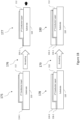
- FIGS 1 and 1A-1E are diagrams illustrating fabrication of a device comprising charge selective transport layers for example embodiments of the present disclosure.
- an exemplary structure begins with a substrate 110.
- the substrate material 110 can be any one or more of a number of substrates suitable for deposition of a conducting film.
- the substrate comprises one or more of a glass, ceramic, plastic and other organic polymers, semiconductor material, a silicon wafer or other wafer material, or similar materials.
- the substrate itself may comprise a photovoltaic cell.
- organic polymers like plastics, include, but are not limited to polyesters such as polyethylene terephthalate (PET) and polyethylene naphthalate (PEN).
- first conductor layer 112 is deposited onto the substrate 110.
- the first conductor layer 112 can be any one or more of a number of conducting materials suitable for collecting charge.
- first conductor layer 112 comprises a transparent conductor.
- a transparent conductor may be implemented using a transparent conducting oxide (TCO), which may include one or more doped metal oxides with considerable conductivity.
- TCO transparent conducting oxide
- the first conductor layer 112 comprises a doped TCO such as indium tin oxide (ITO).
- other materials suitable for fabricating a conductor layer may comprise metal oxides including one or more of many doped metal oxides, including but not limited to: gallium-doped zinc oxide (GZO), indium-doped zinc oxide (IZO), tin-doped indium-oxide (TIO), aluminium-doped zinc-oxide (AZO), indium-doped cadmium-oxide, fluorine-doped tin-oxide (FTO), and combinations thereof.
- GZO gallium-doped zinc oxide
- IZO indium-doped zinc oxide
- TIO tin-doped indium-oxide
- AZO aluminium-doped zinc-oxide
- FTO fluorine-doped tin-oxide
- the first conductor layer 112 can include one or more non-oxide conducting materials, including but not limited to: silver nanowire or carbon nanotube meshes; continuous graphene sheets or small overlapping graphene sheets; highly doped organic semiconducting polymers, including but not limited to poly(ethylenedioxythiophene): poly(styrene sulfonate) (PEDOT:PSS); and TCO nanoparticle films; or any combination thereof.
- non-oxide conducting materials including but not limited to: silver nanowire or carbon nanotube meshes; continuous graphene sheets or small overlapping graphene sheets; highly doped organic semiconducting polymers, including but not limited to poly(ethylenedioxythiophene): poly(styrene sulfonate) (PEDOT:PSS); and TCO nanoparticle films; or any combination thereof.
- the first conductor layer 112 may be employed as a conducting material deposited on top of the substrate 110 (such as shown at 152) or the first conductor layer 112 may be a layer of conductive material embedded within the substrate 110. In still other implementations, the first conductor layer 112 may comprise a layer that is adjacent to the region where the precursor solution 114 is deposited.
- a precursor solution 114 is deposited onto one or both of substrate 110 and first conductor layer 112.
- Precursor solution 114 is deposited in such a way as to facilitate the electrical coupling of what will become the electron transport layer to the first conductor layer 112.
- Some embodiments may optionally include one or more intervening layers (such as a conducting buffer material layer) between the deposited precursor solution 114 and the first conductor layer 112. In such embodiments, the resulting charge selective transport layer will be electrically coupled to the first conductor layer through the buffer material layer.
- the precursor solution 114 is a solution that comprises a metal-containing reactive precursor material that has been mixed with a complexing solvent.
- a metal containing reactive precursor material is a reactive precursor material which includes compounds having a metal atom, M, which is bonded to one or more species, X.
- M metal atom
- X species
- the nature of the M-X bond is such that the molecule readily reacts with water and/or oxygen in an ambient environment in such a way as to convert the M-X bond to a M-O bond, where O represents an oxygen atom, and the H represents a hydrogen atom.
- This reaction may be represented by: M-X n + H 2 O/O 2 ⁇ M-O n (H).
- the O atom may be, but does not necessarily need to be, bonded to a hydrogen atom, H.
- the metal containing reactive precursor may comprise a pyrophoric precursor material, but it need not be pyrophoric.
- the complexing solvent serves to stabilize the reactive metal-containing precursor material, mitigating its reactive nature, enabling the handling of the precursor solution in ambient environments containing oxygen and water without compromising the integrity of the precursor material.
- the precursor material will not react with oxygen or water, and instead will remain complexed with the solvent, over an extended period of time (commonly referred to as the 'shelf-life' of the precursor material).
- the precursor solution 114 may contain a pyrophoric precursor material that is stabilized by dissolving it in a complexing solvent under mild conditions. That is, for such embodiments the precursor solution 114 can be handled at room temperature under normal atmospheric conditions because the complexing solvent renders the solution non-pyrophoric. Utilizing such a precursor solution eliminates the need to provide rigorous oxygen and water-free environments, significantly reducing costs.
- Precursor solution 114 comprises organozinc.
- the reactive metal-containing precursor material is diethylzinc, while in other cases it is dimethylzinc.
- a complexing solvent is defined as a solvent wherein the constituent molecules are capable of donating electron density, generally in the form of an electron lone pair, to an electron deficient molecule, such as in a reactive metal-containing precursor material, thus stabilizing it.
- the complexing solvent generally donates the electron density directly to the otherwise electron-deficient metal atom.
- the complexing solvent comprises at least one of diethyl ether, tetrahydrofuran, diglyme, pyridine, acetonitrile, tetramethylethylenediamine.
- Several methods are available for applying a precursor solution onto the preceding layers of the device that avoids any need for high vacuum and high temperature deposition techniques. These methods include, but are not limited to: slot-die coating, spin-casting, drop-casting, dip-coating, knife coating, spray-coating, ink-jet printing, screen printing, Mayer rod coating, Gravure coating, Flexo printing, or curtain coating.
- precursor solution 114 is deposited onto the substrate 110 and first conductor layer 112 via spin-casting.
- the thickness of the resulting electron-transport layer 116 can be controlled by adjusting the concentration of the precursor in the complexing solvent, and by controlling the spin speed.
- the precursor solution 114 is deposited onto the substrate 110 and first conductor layer 112 by using a technique that is compatible with high-throughput roll-to-roll manufacturing, such as slot-die coating.
- the thickness of the electron transport layer 116 can be controlled by adjusting the concentration of the precursor in the complexing solvent, by controlling the web speed, and/or by controlling the flow rate at which the precursor solution 114 is provided into the process.
- the precursor solution 114 is annealed resulting in the formation of an electron transport layer 116, as shown generally at 158.
- the annealing step can vary in both temperature and time, but due to the reactive nature of the precursor material, the conversion process is generally accomplished at low temperatures that are compatible with a wide variety of substrate and conductor materials. That is, at the temperatures applied, the annealing does not result in adverse degradation of the substrate, conductor or any other prior layer. Both the time and temperature of the annealing can be tailored to the materials utilized.
- the annealing can occur for a period of time ranging from about 1 minute to about 15 minutes.
- the annealing can occur at a temperature ranging from about 100 °C to about 120 °C, which is advantageous for use with sensitive substrate materials, such as polymer substrates in high-throughput roll-to-roll manufacturing conditions, or in the case of sensitive first conductor materials. It should be considered within the skill of one of ordinary skill in the art who has studied the teachings of this disclosure to choose appropriate annealing times and temperatures for the particular precursor, substrate and conductor layer materials they have selected.
- the electron transport layer 116 is positioned between the first conductor layer 112 and an active layer 118.
- Exemplary embodiments of the electron transport layer 116 may have a thickness between 25-200nm. In the laboratory, exemplary embodiments such as those described herein have shown uniformity of the films produced to be at least 90% over large areas. It should be noted that the resulting electron transport layer 116 in some embodiments will comprise the same base materials as a transparent conductor.
- a ZnO electron transport layer may be formed onto a doped ZnO transparent conductor, such as aluminium-doped zinc oxide (AZO).
- AZO aluminium-doped zinc oxide
- Figures 1A and 1B provide illustrations of alternate implementations of the process illustrated in Figure 1 where one or both of the precursor depositions shown at 154 and the annealing shown at 156 are performed through two are more interactive steps.
- FIG. 1A an alternate embodiment is illustrated at 170 and 171 where the precursor solution 114 is deposited as a first precursor solution layer 114-1 followed by deposition of at least one subsequent precursor solution layer 114-2.
- Figure 1A illustrates two precursor layers (114-1 and 114-2), any number of multiple depositions may be performed to form any number of precursor solution layers.
- the plurality of precursor solution layers are then annealed at 156 to form the electron transport layer 116.
- FIG. 1B another embodiment is illustrated where precursor deposition and annealing steps are alternated to form electron transport layer 116. That is, a first precursor solution layer 114-1 is deposited as shown generally at 175. This is followed by an annealing step (shown at 176), which forms a first layer 116-1 of material for the electron transport layer 116 (shown at 177). Then a second precursor solution layer 114-2 is deposited on top of the previously formed electron transport material 116-1 as shown generally at 178. This is followed by another annealing step (shown at 179), which forms a second layer 116-2 of material for the electron transport layer 116 (shown at 180). Multiple iterations of these alternating deposition and annealing steps may be performed until an electron transport layer 116 of the desired thickness is achieved.
- Conductive materials from later applied layers can enter these pinholes degrading the effectiveness of electron transport layer 116 in blocking hole transport. When such pinholes occur, they do so with a random distribution with respect to the upper surface of the layer 116.
- Deposition of layer 116 in multiple passes results in different sub-layers of the electron transport layer 116 with different randomly located pinholes, substantially reducing the probability of any pinhole completely penetrating through the entirety of electron transport layer 116.
- the resulting device will further include an active layer 118 and a second conductor layer 120. It may also include an optional second charge selective transport layer that functions as a hole transport layer 126.
- a first conductive lead 124 is coupled to the first conductor layer 112 and a second conductive lead 122 coupled to the second conductor layer 120.
- the active layer 118 may comprise an appropriate semiconductor junction.
- active layer 118 may comprise a heterojunction, such as a bulk or planar heterojunction, for example.
- the materials used to fabricate active layer 118 may include, but are not limited to, poly(3-hexylthiophene):phenyl C 61 butyric acid methyl ester (P3HT:PCBM) blends, PCPDTBT:PCBM blends, Si-PCPDTBT:PCBM blends, PCDTBT:PCBM blends, PTB7:PC 71 BM blends, or any combinations thereof.
- the second conductor layer 120 can be any one or more of a number of conducting materials suitable for collecting charge such as those mentioned for 1 st conducting layer 112. Further, either of the conductor layers 112 and 120 may comprise one or more metals including, but not limited to magnesium, silver, gold, aluminium, copper, palladium, cadmium, nickel, or zinc. Other optoelectronic devices may be implemented such as, but not limited to: inorganic thin-film PV devices and modules, organic or inorganic light-emitting diodes (LEDs), and organic or inorganic field-effect transistors (FETs).
- LEDs organic or inorganic light-emitting diodes
- FETs organic or inorganic field-effect transistors
- the embodiment shown in Figure 1 at 160 further comprises a hole-transport layer 126 positioned between the active layer 118 and the second conductor layer 120.
- This second charge selective transport layer may be fabricated in the same way as described above for an electron transport layer, but using a second precursor solution having a different selection of metal containing reactive precursor material and a complexing solvent appropriate for that material.
- a precursor solution for a hole transport layer may be prepared by dissolving a metal containing reactive precursor material, such as one containing nickel. This precursor solution may be deposited onto an active layer and annealed into a nickel oxide (NiO) hole transport layer.
- NiO nickel oxide
- a number of other materials can also be used to provide a hole transport layer, including but not limited to such metal oxides as: molybdenum oxide (MoO 3 ), tungsten oxide (WO 3 ), and vanadium oxide (V 2 O 5 ).
- the second precursor solution 121 is deposited onto the surface of the active layer 118 (shown at 162). Any of the solution deposition methods described above for the first precursor material 114 may be utilized to deposit the second precursor material 121, again avoiding the need for high vacuum or high temperature deposition techniques to create this layer.
- the second precursor solution 121 is then annealed (shown at 163) to form a hole transport layer 126 (shown at 164).
- the second conductor layer 120 would then be deposited on the hole transport layer 164 and used to electrically couple an anode for the device to the active layer 118.
- Figures 1D and 1E provide illustrations of alternate implementations of the process illustrated in Figure 1C where one or both of the second precursor depositions shown at 162 and the annealing shown at 163 are performed through two or more interactive steps.
- FIG. 1D an alternate embodiment is illustrated at 165 and 166 where the precursor solution 121 is deposited as a first precursor solution layer 121-1 followed by deposition of at least one subsequent precursor solution layer 121-2.
- Figure 1D illustrates two precursor layers (121-1 and 121-2), any number of multiple depositions may be performed to form any number of precursor solution layers.
- the plurality of precursor solution layer are then annealed at 163 to form the hole transport layer 126.
- FIG. 1E another embodiment is illustrated where precursor deposition and annealing steps are alternated to form hole transport layer 126. That is, a first layer of the second precursor solution 121-1 is deposited as shown generally at 194. This is followed by an annealing step (shown at 195), which forms a first layer 126-1 of material that will form the hole transport layer 126 (shown at 196). Then a second layer of the second precursor solution 121-2 is deposited on top of the previously formed hole transport material 126-1 as shown generally at 197. This is followed by another annealing step (shown at 198), which forms a second layer 126-2 of material for the hole transport layer 126 (shown at 199). Multiple iterations of these alternating deposition and annealing steps may be performed until a hole transport layer 116 of the desired thickness is achieved.
- forming the hole transport layer 126 through multiple depositions of precursor material has the benefit of avoiding pinhole voids that otherwise may form and penetrate completely through the hole transport layer 126.
- Deposition of layer 126 in multiple passes results in different sub-layers of the hole transport layer 126 with different randomly located pinholes, substantially reducing the probability of any pinhole completely penetrating through the entirety of hole transport layer 126.
- the ETL and HTL layers produced as described above can be used in other optoelectronic devices, including but not limited to: inorganic thin-film PV devices and modules, organic or inorganic light-emitting diodes (LEDs), and organic or inorganic field-effect transistors (PETs).
- inorganic thin-film PV devices and modules organic or inorganic light-emitting diodes (LEDs), and organic or inorganic field-effect transistors (PETs).
- LEDs organic or inorganic light-emitting diodes
- PETs organic or inorganic field-effect transistors
- Figure 2 is flow chart illustrating a method 200 for fabricating a charge selective transport layer via one embodiment of the present disclosure.
- the method of Figure 2 is utilized in conjunction with fabrication of a photovoltaic device such as the one described above with respect to any of Figures 1 and 1A-1E .
- Method 200 begins at 210 with providing a precursor solution according to the claims that comprises a metal containing reactive precursor material dissolved into a complexing solvent.
- the metal containing reactive precursor material is a reactive precursor material which includes compounds having a metal atom, M, which is bonded to one or more species, X.
- M metal atom
- X species
- the nature of the M-X bond is such that the molecule readily reacts with water and/or oxygen in an ambient environment to convert the M-X bond to a M-O bond.
- the O atom may be, but does not necessarily need to be, bonded to a hydrogen atom, H.
- the metal containing reactive precursor may comprise a pyrophoric precursor material, but it need not be pyrophoric.
- the complexing solvent is a solvent where constituent molecules are capable of donating electron density, generally in the form of an electron lone pair, to an electron deficient molecule.
- Examples of complexing solvents which may be used at 210 include, diethyl ether, tetrahydrofuran (THF), and diglyme, pyridine, acetonitrile, tetramethylethylenediamine.
- THF tetrahydrofuran
- pyridine tetramethylethylenediamine
- a ZnO electron transport layer is fabricated from a metal containing reactive precursor material such as diethylzinc dissolved into the complexing solvent THF.
- a 10 mL of a 15 wt. % solution of diethylzinc in toluene is mixed with 50 mL of THF in the absence of water and oxygen to produce a precursor solution of 2.5 wt. % diethylzinc/THF/toluene solution.
- the diethylzinc can be mixed directly with THF, without the use of a toluene solution, in the absence of water and oxygen, to produce a precursor solution of 2.5 wt. % diethylzinc/THF solution. Either of such precursor solutions may be used, for example, for formulating precursor solution 114.
- Method 200 proceeds to 220 with depositing the precursor solution onto a surface of a substrate to form a film.
- the film at least in part contacts a first conductor.
- the first conductor's ultimate purpose is to conduct electrons received from the electron transport layer that will be created from the precursor solution.
- the precursor solution is deposited in such a way as to facilitate the electrical coupling of the electron transport layer with the first conductor.
- the first conductor comprises a conductor layer deposited on top of a substrate surface.
- Figure 1 illustrates one such embodiment at 154 where first conductor layer 112 is deposited on top of substrate 110.
- the conductor layer may be a layer of conductive material embedded within the substrate.
- the first conductor may comprise a layer that is adjacent to the region where the precursor solution is deposited.
- one or more intervening layers may exist between the deposited precursor solution 114 and the first conductor.
- the one or more intervening layers either are, or will become, conductive layers that will establish electrical coupling between the electron transport layer and the first conductor.
- the one or more intervening layers may comprise a buffer layer that indirectly couples the electron transport layer to the first conductor.
- Examples of deposition methods which may be used at 220 include, but are not limited to, slot-die coating, spin-casting, drop-casting, dip-coating, knife coating (also known as doctor blading), spray-coating, ink-jet printing, screen printing, Mayer rod coating (also known as metering rod coating), Gravure coating, Flexo printing, and curtain coating.
- the particular method used may be selected based on its compatibility with other manufacturing processes being used.
- the precursor solution is deposited using a technique that is compatible with high-throughput roll-to-roll manufacturing, such as slot-die coating.
- the thickness of the electron transport layer can be controlled, for example, by varying the concentration of the metal containing reactive precursor material mixed with the complexing solvent, by controlling the web speed and/or the flow rate at which the precursor solution is applied to the substrate.
- Method 200 proceeds to 230 with annealing the film to transform the precursor film into an electron transport layer.
- annealing is represented in Figure 1 generally at 156 to form the electron transport layer 116 shown generally at 158 and 160.
- Both the time and temperature of annealing at 230 may be controlled so as to not adversely affect the substrate material or other previously deposited materials.
- typical annealing can be achieved within a period of time ranging from about 1 minute to about 15 minutes and temperatures ranging from about 100 °C to about 120 °C. Such duration and temperatures would, for example, be advantageous for use with substrates, such as polymer substrates used in high-throughput roll-to-roll manufacturing conditions.
- the depositing performed at 220 may comprise slot-die coating of the precursor solution.
- the precursor solution produced from the diethylzinc and THF is slot-die coated onto the substrate at room temperature, in normal ambient atmosphere, to form a film.
- the resulting thin film which will include zinc oxides and hydroxides, is annealed at 230, at a temperature of 100 °C for 5 minutes to produce an electron transport layer comprising a ZnO thin film.
- the uniformity of the films produced has been estimated via UV-visible absorption mapping to be as high as 90% over large areas.
- the work function of the ZnO produced has been measured to be between 4.0 and 4.5 eV by Kelvin probe (referenced to a gold film).
- Conductive materials from later applied layers can enter these pinholes degrading the effectiveness of electron transport layer 116 in blocking hole transport. When such pinholes occur, they do so with a random distribution with respect to the upper surface of the layer 116.
- Deposition of layer 116 in multiple passes results in different sub-layers of the electron transport layer 116 with different randomly located pinholes, substantially reducing the probability of any pinhole completely penetrating through the entirety of electron transport layer 116.
- Figures 2A and 2B provide illustrations of alternate implementations of the process illustrated in Figure 2 where one or both of the precursor deposition shown at 220 and the annealing shown at 230 are performed through two are more interactive steps.
- Forming a charge selective transport layer through multiple depositions of precursor material, as shown by either Figures 2A or 2B or elsewhere in this description, has the benefit of avoiding pinhole voids that otherwise may form an penetrate completely through the electron transport layer for the reasons previously described above.
- 221 comprises depositing a precursor solution onto a surface of a substrate to form a first film layer, where the first film at least in part contracts a 1 st conductor.
- the process then proceeds to 222 with depositing the precursor solution onto a surface of the first film to form a second film layer.
- the process then proceeds to 231 with annealing the first film layer and the second film layer to transform the first film layer and second film layer into an electron transport layer. It would be appreciated that depositing one or more additional layers of the precursor solution onto the previously deposited precursor solutions may be performed before proceeding to 231.
- the plurality of precursor solution layers are then annealed at 231 to form the electron transport layer.
- FIG. 2B another embodiment is illustrated where precursor deposition (block 220) and annealing (block 230) steps are alternated to form the electron transport layer. That is, a first deposition is shown generally at 235 with depositing a precursor solution onto a surface of a substrate to form a first film layer. This deposition may lay the first film so that it at least in part contracts a 1 st conductor, or it may be deposited on an intervening layer that provides a conductive path to the 1 st conductor. The method proceeds with annealing the first film layer to transform the first film layer into a first electron transport layer at 235. Then another layer of precursor solution is applied and annealed.
- the process proceeds with depositing a precursor solution onto a surface of the first electron transport layer to form a second film layer and then to 236 with annealing the second film layer to transform the second film layer and the first electron transport layer into single electron transport layer. Multiple iterations of these alternating deposition and annealing steps may be performed until an electron transport layer of the desired thickness is achieved.
- method 200 may further comprise one or more additional steps to achieve various optional or alternate embodiments for specific applications.
- method 200 proceeds to 240 with forming an active layer on the electron transport layer.
- the particular materials for forming the active layer are selected based on the desired function of the device as already described above for active layer 118 and apply to this method, and as such are not repeated here in detail.
- the placement of the electron transport layer between the active layer and the first conductor will result in a device where electrons are permitted to flow from the active layer to the first conductor, but holes are not, so that an electrical lead coupled to the first conductor will function as the cathode lead for the device (such as mentioned at 250).
- a second conductor is electrically coupled to the active layer such that an electrical lead coupled to the second conductor will function as the anode lead for the device (such as mentioned at 250).
- a hole transport layer is formed on the active layer prior to the second conductor (such as hole transport layer 126 shown in Figure 1 ). Analogous in function to the electron transport layer, the placement of a hole transport layer between the active layer and the second conductor will result in a device where hole current is permitted to flow from the active layer to the second conductor, but electrons are not.
- the forming of the hole transport layer is consistent with the process described above with respect to Figures 1 and 1A-1E .
- the step at 260 comprises depositing a second precursor solution onto a surface of an active layer to form a film. This is followed at 261 with annealing the film to transform the film into a hole transport layer. Also as shown in Figures 2D and 2E , the deposition and annealing can be subdivided into interactive steps.
- the process may comprise depositing a second precursor solution onto a surface of an active layer to form a third film layer (at 262), depositing the second precursor solution onto a surface of the third film layer to form a fourth film layer (at 263) and annealing the third film layer and the fourth film layer to transform the third film layer and fourth film layer into a hole transport layer (at 264, Figure 2E ). It would be appreciated that depositing one or more additional layers of the precursor solution onto the previously deposited precursor solutions may be performed before proceeding to 264. The plurality of precursor solution layers is then annealed at 264 to form the electron transport layer.
- FIG. 2E another embodiment is illustrated at 209 where precursor deposition and annealing steps are alternated to form the hole transport layer. That is, a first deposition is shown generally at 264 with depositing the second precursor solution onto a surface of a substrate to form a third film layer. This deposition may lay the third film layer so that it at least in part contracts the previously deposited active layer, or it may be deposited on an intervening layer that provides a conductive path to the active layer. The method proceeds with annealing the first film layer to transform the third film layer into a first hold transport layer at 265. Then another layer of the second precursor solution is applied and annealed.
- the process proceeds with depositing the second precursor solution onto a surface of the first hole transport layer to form a fourth film layer and then to 267 with annealing the fourth film layer to transform the fourth film layer and the first hole transport layer into a single hole transport layer. Multiple iterations of these alternating deposition and annealing steps may be performed until a hole transport layer of the desired thickness is achieved.
- first conductor and the second conductor may be implemented as transparent conductor layers.
- a single-cell photovoltaic device may be produced by coating the electron transport layer with an active layer that provides a bulk heterojunction (BHJ) solution, followed by a hole-transport layer, and finally depositing a high work-function top electrode, such as silver, for the second conductor.
- BHJ bulk heterojunction
- the electron transport layer serves to facilitate electron extraction and block hole extraction, which helps to maximize the open-circuit voltage (V OC ) from the photovoltaic device.
- J-V current density-voltage
- a ZnO electron transport layer and first conductor layer (which may be a transparent conducting oxide, like indium tin oxide (ITO)), can be patterned to permit formation of discrete cells that are then connected in either a serial or paralleled fashion to yield voltage or current addition, respectively.
- ITO indium tin oxide
- Examples using a convention P1, P2, P3 scribing process, a ZnO/ITO, BHJ, and PEDOT/Ag layers, respectively, can be patterned to produce a serial interconnection of cell stripes to produce modules with additive voltage.
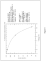
- FIG 4 illustrates a performance plot, certified by the National Renewable Energy Laboratory (NREL), of a large-area Organic Photovoltaic Module incorporating a Zinc Oxide electron transport layer fabricated via an embodiment of the method described herein.
- NREL National Renewable Energy Laboratory
- this Zinc Oxide electron transport layer is quite suitable for use in large-area, high-performance Organic Photovoltaic Modules.
- the favourable V oc demonstrates the effective nature of the ZnO electron transport layer produced from a precursor solution comprising the stabilized diethylzinc solution, and the potential this technology has to enable low-temperature, atmospheric production of inverted-architecture OPV modules in a high-throughput roll-to-roll compatible process.
Landscapes
- Engineering & Computer Science (AREA)
- Manufacturing & Machinery (AREA)
- Physics & Mathematics (AREA)
- Electromagnetism (AREA)
- Electroluminescent Light Sources (AREA)
- Photovoltaic Devices (AREA)
Claims (12)
- Ein Verfahren, das Folgendes beinhaltet:Bilden einer Dünnschicht einer ersten ladungsselektiven Transportschicht (116), die mit einer ersten Leiterschicht (112) auf einem Substrat (110) elektrisch gekoppelt ist,wobei die erste ladungsselektive Transportschicht konfiguriert ist, um Ladungsträger zwischen der ersten Leiterschicht und einer aktiven Schicht (118), die einen Halbleiter beinhaltet, selektiv zu leiten; undBilden der aktiven Schicht, über der ersten ladungsselektiven Transportschicht, wobei die erste ladungsselektive Transportschicht mit der aktiven Schicht elektrisch gekoppelt ist, undwobei das Bilden der ersten ladungsselektiven Transportschicht Folgendes beinhaltet:Ablagern, in einem Umgebungsklima, einer ersten Vorläuferlösung (114), die ein erstes metallhaltiges reaktionsfähiges Vorläufermaterial beinhaltet, das in einem ersten Komplexierungslösungsmittel gelöst ist, um das erste metallhaltige reaktionsfähige Vorläufermaterial zu stabilisieren, sodass es nicht mit Sauerstoff oder Wasser reagieren wird, wobei das erste metallhaltige reaktionsfähige Vorläufermaterial mit dem ersten Komplexierungslösungsmittel in Abwesenheit von Wasser und Sauerstoff gemischt wird, wobei das erste Komplexierungslösungsmittel Moleküle beinhaltet, die fähig sind, Elektronendichte an das erste metallhaltige reaktionsfähige Vorläufermaterial abzugeben, wobei das erste Komplexierungslösungsmittel mindestens eines von Tetrahydrofuran (THF), Diethylether, Diethylenglykoldimethylether (diglyme), Pyridin, Acetonitril oder Tetramethylethylendiamin beinhaltet und das erste metallhaltige reaktionsfähige Vorläufermaterial Moleküle beinhaltet, die ein Metallatom, M, aufweisen, das mit einer oder mehreren Spezies, X, in einer M-X-Bindung verbunden ist, sodass, wenn die Moleküle des ersten metallhaltigen reaktionsfähigen Vorläufermaterials mit dem mindestens einen von Wasser oder Sauerstoff in dem Umgebungsklima reagieren, die M-X-Bindung in eine M-O-Bindung umgewandelt wird, wobei O ein Sauerstoffatom darstellt, wobei das erste metallhaltige reaktionsfähige Vorläufermaterial Organozink beinhaltet;wodurch gestattet wird, dass das erste metallhaltige reaktionsfähige Vorläufermaterial mit mindestens einem von Wasser oder Sauerstoff in dem Umgebungsklima reagiert, um ein erstes Flächengebilde zu bilden; undTempern des ersten Flächengebildes über einen Zeitraum im Bereich von etwa 1 Minute bis etwa 15 Minuten und bei einer Temperatur von etwa 100 Grad Celsius bis etwa 120 Grad Celsius, wodurch die M-X-Bindung des ersten metallhaltigen reaktionsfähigen Vorläufermaterials in eine M-O-Bindung umgewandelt wird, um die erste ladungsselektive Transportschicht zu bilden.
- Verfahren gemäß Anspruch 1, wobei die erste ladungsselektive Transportschicht auf der ersten Leiterschicht gebildet wird und diese mindestens teilweise berührt.
- Verfahren gemäß Anspruch 1, wobei die erste ladungsselektive Transportschicht auf mindestens einer Zwischenschicht gebildet wird, die ein Material beinhaltet, das die erste ladungsselektive Transportschicht mit der ersten Leiterschicht elektrisch koppelt.
- Verfahren gemäß Anspruch 1, wobei das erste Flächengebilde eine Elektronentransportschicht bildet, wenn es getempert wird.
- Verfahren gemäß Anspruch 1, wobei das erste Flächengebilde eine Lochtransportschicht bildet, wenn es getempert wird.
- Verfahren gemäß Anspruch 1, das ferner Folgendes beinhaltet:Bereitstellen einer zweiten Vorläuferlösung, die ein zweites metallhaltiges reaktionsfähiges Vorläufermaterial beinhaltet, das in einem zweiten Komplexierungslösungsmittel gelöst ist; Ablagern der Vorläuferlösung auf einer Oberfläche eines zweiten Substrats, um ein zweites Flächengebilde zu bilden;Bilden einer zweiten ladungsselektiven Transportschicht auf dem zweiten Substrat durch Tempern des Flächengebildes;Bilden eines zweiten Leiters, der mit der zweiten ladungsselektiven Transportschicht elektrisch gekoppelt ist.
- Verfahren gemäß Anspruch 6, wobei das erste Flächengebilde eine Elektronentransportschicht bildet, wenn es getempert wird, und wobei das zweite Flächengebilde eine Lochtransportschicht bildet, wenn es getempert wird.
- Verfahren gemäß Anspruch 1, wobei die aktive Schicht einen Halbleiterheteroübergang beinhaltet.
- Verfahren gemäß Anspruch 1, wobei das erste metallhaltige reaktionsfähige Vorläufermaterial Diethylzink oder Dimethylzink beinhaltet.
- Verfahren gemäß Anspruch 1, wobei die erste ladungsselektive Transportschicht ein ZnO-Flächengebilde beinhaltet.
- Verfahren gemäß Anspruch 1, wobei das Ablagern der ersten Vorläuferlösung mindestens eines von Folgenden beinhaltet: Schlitzbeschichtung, Schleuderguss, Tropfbeschichtung, Tauchbeschichtung, Rakelauftrag, Spritzbeschichtung, Tintenstrahldruck, Schablonendruck, Mayerstangenbeschichtung, Gravurstreichverfahren, Flexodruck oder Florstreichverfahren.
- Verfahren gemäß Anspruch 1, wobei die erste Leiterschicht ein transparentes Leitermaterial beinhaltet.
Applications Claiming Priority (2)
| Application Number | Priority Date | Filing Date | Title |
|---|---|---|---|
| US201361774200P | 2013-03-07 | 2013-03-07 | |
| PCT/US2014/021665 WO2014138558A1 (en) | 2013-03-07 | 2014-03-07 | Methods for producing thin film charge selective transport layers |
Publications (5)
| Publication Number | Publication Date |
|---|---|
| EP2965366A1 EP2965366A1 (de) | 2016-01-13 |
| EP2965366A4 EP2965366A4 (de) | 2016-12-07 |
| EP2965366B1 EP2965366B1 (de) | 2024-05-22 |
| EP2965366C0 EP2965366C0 (de) | 2024-05-22 |
| EP2965366B9 true EP2965366B9 (de) | 2024-08-14 |
Family
ID=51488303
Family Applications (1)
| Application Number | Title | Priority Date | Filing Date |
|---|---|---|---|
| EP14760234.6A Active EP2965366B9 (de) | 2013-03-07 | 2014-03-07 | Verfahren zur herstellung von dünnschicht-ladungsselektiven transportschichten |
Country Status (5)
| Country | Link |
|---|---|
| US (1) | US9859515B2 (de) |
| EP (1) | EP2965366B9 (de) |
| CN (1) | CN106463626B (de) |
| CA (1) | CA2925436C (de) |
| WO (1) | WO2014138558A1 (de) |
Families Citing this family (20)
| Publication number | Priority date | Publication date | Assignee | Title |
|---|---|---|---|---|
| US20120132272A1 (en) | 2010-11-19 | 2012-05-31 | Alliance For Sustainable Energy, Llc. | Solution processed metal oxide thin film hole transport layers for high performance organic solar cells |
| US10714269B2 (en) | 2014-11-20 | 2020-07-14 | Brown University | Method of making coated substrates |
| US9786856B2 (en) * | 2015-08-20 | 2017-10-10 | Dpix, Llc | Method of manufacturing an image sensor device |
| US10763778B2 (en) * | 2015-12-09 | 2020-09-01 | Brian Patrick Janowski | Solar window construction and methods |
| US10211776B2 (en) | 2015-12-09 | 2019-02-19 | Brian Patrick Janowski | Solar window construction and methods |
| US11489483B2 (en) | 2015-12-09 | 2022-11-01 | Brian Patrick Janowski | Solar window construction and methods |
| US9711722B2 (en) * | 2015-12-15 | 2017-07-18 | Institute of Nuclear Energy Research, Atomic Energy Council, Executive Yuan, R.O.C. | Method for improving mass-production yield of large-area organic solar cells |
| US20170179199A1 (en) * | 2015-12-18 | 2017-06-22 | Dpix, Llc | Method of screen printing in manufacturing an image sensor device |
| MX393060B (es) * | 2016-03-04 | 2025-03-24 | Solarwindow Tech Inc | Sistemas y métodos para dispositivos semiconductores orgánicos con capas de contacto por pulverización catódica. |
| JP7246126B2 (ja) * | 2016-12-27 | 2023-03-27 | 株式会社リコー | 光電変換素子 |
| CN106876599B (zh) * | 2017-03-10 | 2019-07-16 | 纳晶科技股份有限公司 | 无机金属化合物、含其的组合物、器件和装置及制作方法 |
| US11205753B2 (en) * | 2017-04-25 | 2021-12-21 | The Hong Kong University Of Science And Technology | Use of sequential processing for highly efficient organic solar cells based on conjugated polymers with temperature dependent aggregation |
| US11127698B2 (en) * | 2017-07-07 | 2021-09-21 | Toray Industries, Inc. | Method for producing conductive film, method for producing field effect transistor using same, and method for producing wireless communication device |
| US20190309422A1 (en) * | 2018-04-06 | 2019-10-10 | Versum Materials Us, Llc | Spin-On Metallization |
| CN111384273B (zh) * | 2018-12-29 | 2021-07-16 | Tcl科技集团股份有限公司 | 一种量子点发光二极管及其制备方法 |
| CN111584766A (zh) * | 2020-05-27 | 2020-08-25 | 合肥福纳科技有限公司 | 量子点发光二极管的制备方法及制得的量子点发光二极管 |
| CN114695583B (zh) * | 2020-12-25 | 2023-12-05 | 泰州隆基乐叶光伏科技有限公司 | 太阳电池及生产方法、光伏组件 |
| CN113675340B (zh) * | 2021-08-20 | 2024-05-17 | 广西大学 | 基于钙钛矿/pdpp3t聚合物复合膜的近红外宽光谱探测器及其制备方法 |
| US12481327B1 (en) * | 2021-11-11 | 2025-11-25 | Alexandrine Blais | Mobile telephone case with fence tester |
| JP2025500452A (ja) | 2021-12-22 | 2025-01-09 | ネイバーズ エナジー トランジション ソリューションズ エルエルシー | 硫黄ドープ炭素系ナノ材料及びそれを形成する方法 |
Family Cites Families (53)
| Publication number | Priority date | Publication date | Assignee | Title |
|---|---|---|---|---|
| JPS61281047A (ja) | 1985-06-06 | 1986-12-11 | Nippon Sheet Glass Co Ltd | 二酸化珪素被膜の製造方法 |
| US5776254A (en) | 1994-12-28 | 1998-07-07 | Mitsubishi Denki Kabushiki Kaisha | Apparatus for forming thin film by chemical vapor deposition |
| US6126740A (en) | 1995-09-29 | 2000-10-03 | Midwest Research Institute | Solution synthesis of mixed-metal chalcogenide nanoparticles and spray deposition of precursor films |
| US5711803A (en) | 1995-09-29 | 1998-01-27 | Midwest Research Institute | Preparation of a semiconductor thin film |
| DE60021663T2 (de) | 1999-01-21 | 2006-05-24 | Midwest Research Institute | Passivierungsätzmittel für metallpartikel |
| EP1441864B1 (de) | 2000-01-21 | 2009-11-18 | Midwest Research Institute | Verfahren zur herstellung von dünnfilmleitern durch zersetzung von metallchelaten in verbindung mit metallteilchen |
| US20060001726A1 (en) | 2001-10-05 | 2006-01-05 | Cabot Corporation | Printable conductive features and processes for making same |
| US6951666B2 (en) | 2001-10-05 | 2005-10-04 | Cabot Corporation | Precursor compositions for the deposition of electrically conductive features |
| EP1468054A1 (de) | 2001-11-01 | 2004-10-20 | Yissum Research Development Company of the Hebrew University of Jerusalem | Tintenstrahldrucktinten mit nantoteilchen aus metall |
| US6951694B2 (en) | 2002-03-29 | 2005-10-04 | The University Of Southern California | Organic light emitting devices with electron blocking layers |
| KR100765684B1 (ko) | 2002-07-03 | 2007-10-11 | 삼성전자주식회사 | 합금 패턴 형성용 유기금속 전구체 혼합물 및 이를 이용한합금 패턴 형성방법 |
| JP4185341B2 (ja) | 2002-09-25 | 2008-11-26 | パイオニア株式会社 | 多層バリア膜構造、有機エレクトロルミネッセンス表示パネル及び製造方法 |
| US7535017B2 (en) | 2003-05-30 | 2009-05-19 | Osram Opto Semiconductors Gmbh | Flexible multilayer packaging material and electronic devices with the packaging material |
| US7170001B2 (en) | 2003-06-26 | 2007-01-30 | Advent Solar, Inc. | Fabrication of back-contacted silicon solar cells using thermomigration to create conductive vias |
| US7094709B2 (en) | 2004-06-15 | 2006-08-22 | Braggone Oy | Method of synthesizing hybrid metal oxide materials and applications thereof |
| US20050288555A1 (en) | 2004-06-28 | 2005-12-29 | Binmoeller Kenneth E | Methods and devices for illuminating, vievwing and monitoring a body cavity |
| US7214922B2 (en) | 2004-09-17 | 2007-05-08 | Kabushiki Kaisha Toshiba | Semiconductor photosensor device and information apparatus with sensitivity region for wide dynamic range |
| US8026510B2 (en) * | 2004-10-20 | 2011-09-27 | Dai Nippon Printing Co., Ltd. | Organic electronic device and method for producing the same |
| US20060115673A1 (en) * | 2004-12-01 | 2006-06-01 | Au Optronics Corporation | Organic light emitting device with improved electrode structure |
| EP1829132B8 (de) | 2004-12-23 | 2010-11-24 | Technische Universität Braunschweig | Material für eine dotierte und undotierte loch- und elektronentransportschicht |
| US20060208257A1 (en) | 2005-03-15 | 2006-09-21 | Branz Howard M | Method for low-temperature, hetero-epitaxial growth of thin film cSi on amorphous and multi-crystalline substrates and c-Si devices on amorphous, multi-crystalline, and crystalline substrates |
| US7556748B2 (en) | 2005-04-14 | 2009-07-07 | E. I. Du Pont De Nemours And Company | Method of manufacture of semiconductor device and conductive compositions used therein |
| US8093491B2 (en) | 2005-06-03 | 2012-01-10 | Ferro Corporation | Lead free solar cell contacts |
| US20070163634A1 (en) | 2005-07-14 | 2007-07-19 | Kyocera Corporation | Solar cell, manufacturing method and manufacturing management system thereof, and solar cell module |
| NO20061668L (no) | 2006-04-12 | 2007-10-15 | Renewable Energy Corp | Solcelle og fremgangsmate for fremstilling av samme |
| US20080003364A1 (en) | 2006-06-28 | 2008-01-03 | Ginley David S | Metal Inks |
| US7491575B2 (en) * | 2006-08-02 | 2009-02-17 | Xerox Corporation | Fabricating zinc oxide semiconductor using hydrolysis |
| KR101130199B1 (ko) | 2006-11-06 | 2012-04-23 | 에이전시 포 사이언스, 테크놀로지 앤드 리서치 | 나노입자 캡슐 배리어 스택 |
| WO2008063190A2 (en) | 2006-11-09 | 2008-05-29 | Midwest Research Institute | Precursors for formation of copper selenide, indium selenide, copper indium diselenide, and/or copper indium gallium diselenide films |
| TW200838008A (en) | 2006-12-04 | 2008-09-16 | Asahi Chemical Ind | Method for producing electronic device and coating solutions suitable for the production method |
| US7799990B2 (en) | 2007-03-12 | 2010-09-21 | Northwestern University | Electron-blocking layer / hole-transport layer for organic photovoltaics and applications of same |
| WO2009026097A1 (en) | 2007-08-17 | 2009-02-26 | Northwestern University | P-type semiconducting nickel oxide as an efficiency-enhancing anodal interfacial layer in bulk heterojunction solar cells |
| US8759144B2 (en) | 2007-11-02 | 2014-06-24 | Alliance For Sustainable Energy, Llc | Fabrication of contacts for silicon solar cells including printing burn through layers |
| US20100209594A1 (en) | 2007-11-02 | 2010-08-19 | Alliance For Sustainable Energy, Llc | Printing aluminum films and patterned contacts using organometallic precursor inks |
| US8308993B2 (en) | 2008-01-30 | 2012-11-13 | Basf Se | Conductive inks |
| JP5205085B2 (ja) | 2008-03-12 | 2013-06-05 | 富士フイルム株式会社 | 有機光電変換材料および有機薄膜光電変換素子 |
| JP5319962B2 (ja) | 2008-05-30 | 2013-10-16 | 富士フイルム株式会社 | 有機薄膜光電変換素子およびその製造方法 |
| US9295133B2 (en) | 2008-07-17 | 2016-03-22 | The Regents Of The University Of California | Solution processable material for electronic and electro-optic applications |
| EP2431330B1 (de) | 2009-04-21 | 2019-02-27 | Tosoh Finechem Corporation | Zusammensetzung zum formen dotierter oder nichtdotierter zinkoxid-dünnschichten sowie verfahren zur herstellung von zinkoxid-dünnschichten damit |
| AU2010254629B2 (en) | 2009-06-02 | 2015-01-22 | Agency For Science, Technology And Research | Multilayer barrier film |
| JP2011027549A (ja) | 2009-07-24 | 2011-02-10 | Sumitomo Electric Ind Ltd | コンタクトプローブ及びその製造方法 |
| CN101707237B (zh) * | 2009-10-30 | 2011-08-17 | 彩虹集团公司 | 一种柔性有机电致发光器件的封装结构及其封装方法 |
| US20120216870A1 (en) | 2009-11-03 | 2012-08-30 | University Of Florida Research Foundation Inc. | Interlayer for organic solar cells |
| KR20110051821A (ko) | 2009-11-11 | 2011-05-18 | 한국기계연구원 | 유기태양전지의 P형 전도막으로 사용되는 NiO 전도막, 이의 제조방법 및 이를 포함하는 광전변환효율이 향상된 유기태양전지 |
| CN101710611A (zh) * | 2009-12-08 | 2010-05-19 | 天津理工大学 | 一种结构新颖的双蓝光发射层有机电致发光器件 |
| CN101728491B (zh) * | 2009-12-21 | 2012-09-05 | 中国科学院长春应用化学研究所 | 一种白色有机发光器件及其制备方法 |
| US9175397B2 (en) * | 2010-03-15 | 2015-11-03 | Alliance For Sustainable Energy, Llc | Multilayer heterostructures and their manufacture |
| US8404302B2 (en) | 2010-07-14 | 2013-03-26 | Sharp Laboratories Of America, Inc. | Solution process for fabricating a textured transparent conductive oxide (TCO) |
| CN101916830B (zh) * | 2010-07-14 | 2012-05-02 | 中国科学院长春应用化学研究所 | 白色有机电致发光器件及其制备方法 |
| US8735718B2 (en) | 2010-09-13 | 2014-05-27 | University Of Central Florida | Electrode structure, method and applications |
| KR101131564B1 (ko) | 2010-10-27 | 2012-04-04 | 한국기계연구원 | 코어/쉘 금속산화물 나노입자를 이용한 효율적인 유기태양전지 및 이의 제조방법 |
| US20120132272A1 (en) | 2010-11-19 | 2012-05-31 | Alliance For Sustainable Energy, Llc. | Solution processed metal oxide thin film hole transport layers for high performance organic solar cells |
| US8889471B2 (en) | 2011-05-09 | 2014-11-18 | Sichuan Yinhe Chemical Co., Ltd. | Burnthrough formulations |
-
2014
- 2014-03-07 EP EP14760234.6A patent/EP2965366B9/de active Active
- 2014-03-07 US US14/200,315 patent/US9859515B2/en active Active
- 2014-03-07 CA CA2925436A patent/CA2925436C/en active Active
- 2014-03-07 WO PCT/US2014/021665 patent/WO2014138558A1/en not_active Ceased
- 2014-03-07 CN CN201480026341.4A patent/CN106463626B/zh active Active
Also Published As
| Publication number | Publication date |
|---|---|
| CA2925436A1 (en) | 2014-09-12 |
| US20140256081A1 (en) | 2014-09-11 |
| EP2965366A4 (de) | 2016-12-07 |
| EP2965366B1 (de) | 2024-05-22 |
| WO2014138558A1 (en) | 2014-09-12 |
| CA2925436C (en) | 2021-10-26 |
| EP2965366C0 (de) | 2024-05-22 |
| CN106463626A (zh) | 2017-02-22 |
| US9859515B2 (en) | 2018-01-02 |
| CN106463626B (zh) | 2020-11-13 |
| EP2965366A1 (de) | 2016-01-13 |
Similar Documents
| Publication | Publication Date | Title |
|---|---|---|
| EP2965366B9 (de) | Verfahren zur herstellung von dünnschicht-ladungsselektiven transportschichten | |
| Meng et al. | Improving the stability of bulk heterojunction solar cells by incorporating pH-neutral PEDOT: PSS as the hole transport layer | |
| KR101310058B1 (ko) | 역구조 유기 태양전지 및 그 제조방법 | |
| Hietzschold et al. | Functionalized nickel oxide hole contact layers: work function versus conductivity | |
| TWI503050B (zh) | 用於透光裝置的導電結構 | |
| Yu et al. | Titanium nitride electron-conductive contact for silicon solar cells by radio frequency sputtering from a TiN target | |
| Aslan et al. | Sol–gel derived In2S3 buffer layers for inverted organic photovoltaic cells | |
| WO2015077629A1 (en) | Devices, structures, materials and methods for vertical light emitting transistors and light emitting displays | |
| US10580983B2 (en) | Ultra-fast method for formation of organic/inorganic thin film by using spontaneous spreading effect | |
| Hoye et al. | High performance inverted bulk heterojunction solar cells by incorporation of dense, thin ZnO layers made using atmospheric atomic layer deposition | |
| Choi et al. | ZnO–Ag–MoO3 transparent composite electrode for ITO-free, PEDOT: PSS-free bulk-heterojunction organic solar cells | |
| US20230167326A1 (en) | Methods for Forming Perovskite Material Layers | |
| EP2671269A1 (de) | Photovoltaische zellen | |
| KR101282564B1 (ko) | 유기용매를 첨가한 전도성 유기박막의 제조방법 및 이를 이용한 유기태양전지 | |
| Choi et al. | Optimized activation of solution‐processed amorphous oxide semiconductors for flexible transparent conductive electrodes | |
| JP2010283313A (ja) | 酸化インジウムスズito立体電極、その製造方法、製造装置、及びそのソーラー電池の製造方法 | |
| CN107629642B (zh) | 功函可调的聚合物复合材料、其制备方法及应用 | |
| KR102032012B1 (ko) | 유기 전자소자, 태양전지 및 그의 제조방법 | |
| CN1697104A (zh) | 含有有机异质结的电接触材料及其器件 | |
| Liu et al. | Unravelling the electrical field induced ion migration in flexible OLEDs with PEDOT: PSS electrodes | |
| KR20180035057A (ko) | 유기 태양전지 및 이의 제조 방법 | |
| CN101931053A (zh) | 氧化铟锡立体电极及制法及制备装置及太阳能电池制法 | |
| Ge et al. | High fill factor over 82% enabled by a biguanide doping electron transporting layer in planar perovskite solar cells | |
| KR101316237B1 (ko) | 용액 공정 기반의 정공 전도층 제조방법 및 이를 이용한 유기태양전지의 제조방법 | |
| KR101412511B1 (ko) | 병렬저항이 극대화된 유기 태양전지 및 그 제조방법 |
Legal Events
| Date | Code | Title | Description |
|---|---|---|---|
| PUAI | Public reference made under article 153(3) epc to a published international application that has entered the european phase |
Free format text: ORIGINAL CODE: 0009012 |
|
| 17P | Request for examination filed |
Effective date: 20151007 |
|
| AK | Designated contracting states |
Kind code of ref document: A1 Designated state(s): AL AT BE BG CH CY CZ DE DK EE ES FI FR GB GR HR HU IE IS IT LI LT LU LV MC MK MT NL NO PL PT RO RS SE SI SK SM TR |
|
| AX | Request for extension of the european patent |
Extension state: BA ME |
|
| DAX | Request for extension of the european patent (deleted) | ||
| A4 | Supplementary search report drawn up and despatched |
Effective date: 20161107 |
|
| RIC1 | Information provided on ipc code assigned before grant |
Ipc: H01L 51/46 20060101AFI20161031BHEP |
|
| STAA | Information on the status of an ep patent application or granted ep patent |
Free format text: STATUS: REQUEST FOR EXAMINATION WAS MADE |
|
| STAA | Information on the status of an ep patent application or granted ep patent |
Free format text: STATUS: THE APPLICATION IS DEEMED TO BE WITHDRAWN |
|
| 18D | Application deemed to be withdrawn |
Effective date: 20170607 |
|
| 18RA | Request filed for re-establishment of rights before grant |
Effective date: 20180525 |
|
| 18RR | Decision to grant the request for re-establishment of rights before grant |
Free format text: ANGENOMMEN Effective date: 20200131 |
|
| STAA | Information on the status of an ep patent application or granted ep patent |
Free format text: STATUS: REQUEST FOR EXAMINATION WAS MADE |
|
| D18D | Application deemed to be withdrawn (deleted) | ||
| STAA | Information on the status of an ep patent application or granted ep patent |
Free format text: STATUS: EXAMINATION IS IN PROGRESS |
|
| 17Q | First examination report despatched |
Effective date: 20200828 |
|
| REG | Reference to a national code |
Ref country code: DE Ref legal event code: R079 Free format text: PREVIOUS MAIN CLASS: H01L0051460000 Ipc: H10K0071400000 Ref country code: DE Ref legal event code: R079 Ref document number: 602014090211 Country of ref document: DE Free format text: PREVIOUS MAIN CLASS: H01L0051460000 Ipc: H10K0071400000 |
|
| RIC1 | Information provided on ipc code assigned before grant |
Ipc: H10K 30/50 20230101ALN20230919BHEP Ipc: H10K 85/20 20230101ALN20230919BHEP Ipc: H10K 85/10 20230101ALN20230919BHEP Ipc: H10K 71/40 20230101AFI20230919BHEP |
|
| RIC1 | Information provided on ipc code assigned before grant |
Ipc: H10K 30/50 20230101ALN20231009BHEP Ipc: H10K 85/20 20230101ALN20231009BHEP Ipc: H10K 85/10 20230101ALN20231009BHEP Ipc: H10K 71/40 20230101AFI20231009BHEP |
|
| RIC1 | Information provided on ipc code assigned before grant |
Ipc: H10K 30/50 20230101ALN20231023BHEP Ipc: H10K 85/20 20230101ALN20231023BHEP Ipc: H10K 85/10 20230101ALN20231023BHEP Ipc: H10K 71/40 20230101AFI20231023BHEP |
|
| RIC1 | Information provided on ipc code assigned before grant |
Ipc: H10K 30/50 20230101ALN20231027BHEP Ipc: H10K 85/20 20230101ALN20231027BHEP Ipc: H10K 85/10 20230101ALN20231027BHEP Ipc: H10K 71/40 20230101AFI20231027BHEP |
|
| RIC1 | Information provided on ipc code assigned before grant |
Ipc: H10K 30/50 20230101ALN20231108BHEP Ipc: H10K 85/20 20230101ALN20231108BHEP Ipc: H10K 85/10 20230101ALN20231108BHEP Ipc: H10K 71/40 20230101AFI20231108BHEP |
|
| GRAP | Despatch of communication of intention to grant a patent |
Free format text: ORIGINAL CODE: EPIDOSNIGR1 |
|
| STAA | Information on the status of an ep patent application or granted ep patent |
Free format text: STATUS: GRANT OF PATENT IS INTENDED |
|
| RIC1 | Information provided on ipc code assigned before grant |
Ipc: H10K 30/50 20230101ALN20231115BHEP Ipc: H10K 85/20 20230101ALN20231115BHEP Ipc: H10K 85/10 20230101ALN20231115BHEP Ipc: H10K 71/40 20230101AFI20231115BHEP |
|
| RIC1 | Information provided on ipc code assigned before grant |
Ipc: H10K 30/50 20230101ALN20231122BHEP Ipc: H10K 85/20 20230101ALN20231122BHEP Ipc: H10K 85/10 20230101ALN20231122BHEP Ipc: H10K 71/40 20230101AFI20231122BHEP |
|
| RIC1 | Information provided on ipc code assigned before grant |
Ipc: H10K 30/50 20230101ALN20231127BHEP Ipc: H10K 85/20 20230101ALN20231127BHEP Ipc: H10K 85/10 20230101ALN20231127BHEP Ipc: H10K 71/40 20230101AFI20231127BHEP |
|
| INTG | Intention to grant announced |
Effective date: 20231218 |
|
| RAP1 | Party data changed (applicant data changed or rights of an application transferred) |
Owner name: SOLARWINDOW TECHNOLOGIES, INC |
|
| GRAS | Grant fee paid |
Free format text: ORIGINAL CODE: EPIDOSNIGR3 |
|
| GRAA | (expected) grant |
Free format text: ORIGINAL CODE: 0009210 |
|
| STAA | Information on the status of an ep patent application or granted ep patent |
Free format text: STATUS: THE PATENT HAS BEEN GRANTED |
|
| AK | Designated contracting states |
Kind code of ref document: B1 Designated state(s): AL AT BE BG CH CY CZ DE DK EE ES FI FR GB GR HR HU IE IS IT LI LT LU LV MC MK MT NL NO PL PT RO RS SE SI SK SM TR |
|
| RAP3 | Party data changed (applicant data changed or rights of an application transferred) |
Owner name: SOLARWINDOW TECHNOLOGIES, INC. |
|
| REG | Reference to a national code |
Ref country code: CH Ref legal event code: EP |
|
| REG | Reference to a national code |
Ref country code: DE Ref legal event code: R096 Ref document number: 602014090211 Country of ref document: DE |
|
| REG | Reference to a national code |
Ref country code: IE Ref legal event code: FG4D |
|
| U01 | Request for unitary effect filed |
Effective date: 20240618 |
|
| REG | Reference to a national code |
Ref country code: CH Ref legal event code: PK Free format text: BERICHTIGUNG B9 |
|
| U07 | Unitary effect registered |
Designated state(s): AT BE BG DE DK EE FI FR IT LT LU LV MT NL PT SE SI Effective date: 20240715 |
|
| PG25 | Lapsed in a contracting state [announced via postgrant information from national office to epo] |
Ref country code: IS Free format text: LAPSE BECAUSE OF FAILURE TO SUBMIT A TRANSLATION OF THE DESCRIPTION OR TO PAY THE FEE WITHIN THE PRESCRIBED TIME-LIMIT Effective date: 20240922 |
|
| PG25 | Lapsed in a contracting state [announced via postgrant information from national office to epo] |
Ref country code: HR Free format text: LAPSE BECAUSE OF FAILURE TO SUBMIT A TRANSLATION OF THE DESCRIPTION OR TO PAY THE FEE WITHIN THE PRESCRIBED TIME-LIMIT Effective date: 20240522 |
|
| PG25 | Lapsed in a contracting state [announced via postgrant information from national office to epo] |
Ref country code: GR Free format text: LAPSE BECAUSE OF FAILURE TO SUBMIT A TRANSLATION OF THE DESCRIPTION OR TO PAY THE FEE WITHIN THE PRESCRIBED TIME-LIMIT Effective date: 20240823 |
|
| PG25 | Lapsed in a contracting state [announced via postgrant information from national office to epo] |
Ref country code: ES Free format text: LAPSE BECAUSE OF FAILURE TO SUBMIT A TRANSLATION OF THE DESCRIPTION OR TO PAY THE FEE WITHIN THE PRESCRIBED TIME-LIMIT Effective date: 20240522 |
|
| PG25 | Lapsed in a contracting state [announced via postgrant information from national office to epo] |
Ref country code: PL Free format text: LAPSE BECAUSE OF FAILURE TO SUBMIT A TRANSLATION OF THE DESCRIPTION OR TO PAY THE FEE WITHIN THE PRESCRIBED TIME-LIMIT Effective date: 20240522 |
|
| PG25 | Lapsed in a contracting state [announced via postgrant information from national office to epo] |
Ref country code: PL Free format text: LAPSE BECAUSE OF FAILURE TO SUBMIT A TRANSLATION OF THE DESCRIPTION OR TO PAY THE FEE WITHIN THE PRESCRIBED TIME-LIMIT Effective date: 20240522 Ref country code: NO Free format text: LAPSE BECAUSE OF FAILURE TO SUBMIT A TRANSLATION OF THE DESCRIPTION OR TO PAY THE FEE WITHIN THE PRESCRIBED TIME-LIMIT Effective date: 20240822 Ref country code: IS Free format text: LAPSE BECAUSE OF FAILURE TO SUBMIT A TRANSLATION OF THE DESCRIPTION OR TO PAY THE FEE WITHIN THE PRESCRIBED TIME-LIMIT Effective date: 20240922 Ref country code: HR Free format text: LAPSE BECAUSE OF FAILURE TO SUBMIT A TRANSLATION OF THE DESCRIPTION OR TO PAY THE FEE WITHIN THE PRESCRIBED TIME-LIMIT Effective date: 20240522 Ref country code: GR Free format text: LAPSE BECAUSE OF FAILURE TO SUBMIT A TRANSLATION OF THE DESCRIPTION OR TO PAY THE FEE WITHIN THE PRESCRIBED TIME-LIMIT Effective date: 20240823 Ref country code: ES Free format text: LAPSE BECAUSE OF FAILURE TO SUBMIT A TRANSLATION OF THE DESCRIPTION OR TO PAY THE FEE WITHIN THE PRESCRIBED TIME-LIMIT Effective date: 20240522 Ref country code: RS Free format text: LAPSE BECAUSE OF FAILURE TO SUBMIT A TRANSLATION OF THE DESCRIPTION OR TO PAY THE FEE WITHIN THE PRESCRIBED TIME-LIMIT Effective date: 20240822 |
|
| PG25 | Lapsed in a contracting state [announced via postgrant information from national office to epo] |
Ref country code: CZ Free format text: LAPSE BECAUSE OF FAILURE TO SUBMIT A TRANSLATION OF THE DESCRIPTION OR TO PAY THE FEE WITHIN THE PRESCRIBED TIME-LIMIT Effective date: 20240522 |
|
| PG25 | Lapsed in a contracting state [announced via postgrant information from national office to epo] |
Ref country code: SK Free format text: LAPSE BECAUSE OF FAILURE TO SUBMIT A TRANSLATION OF THE DESCRIPTION OR TO PAY THE FEE WITHIN THE PRESCRIBED TIME-LIMIT Effective date: 20240522 Ref country code: RO Free format text: LAPSE BECAUSE OF FAILURE TO SUBMIT A TRANSLATION OF THE DESCRIPTION OR TO PAY THE FEE WITHIN THE PRESCRIBED TIME-LIMIT Effective date: 20240522 |
|
| PG25 | Lapsed in a contracting state [announced via postgrant information from national office to epo] |
Ref country code: SM Free format text: LAPSE BECAUSE OF FAILURE TO SUBMIT A TRANSLATION OF THE DESCRIPTION OR TO PAY THE FEE WITHIN THE PRESCRIBED TIME-LIMIT Effective date: 20240522 |
|
| PG25 | Lapsed in a contracting state [announced via postgrant information from national office to epo] |
Ref country code: SM Free format text: LAPSE BECAUSE OF FAILURE TO SUBMIT A TRANSLATION OF THE DESCRIPTION OR TO PAY THE FEE WITHIN THE PRESCRIBED TIME-LIMIT Effective date: 20240522 Ref country code: SK Free format text: LAPSE BECAUSE OF FAILURE TO SUBMIT A TRANSLATION OF THE DESCRIPTION OR TO PAY THE FEE WITHIN THE PRESCRIBED TIME-LIMIT Effective date: 20240522 Ref country code: RO Free format text: LAPSE BECAUSE OF FAILURE TO SUBMIT A TRANSLATION OF THE DESCRIPTION OR TO PAY THE FEE WITHIN THE PRESCRIBED TIME-LIMIT Effective date: 20240522 Ref country code: CZ Free format text: LAPSE BECAUSE OF FAILURE TO SUBMIT A TRANSLATION OF THE DESCRIPTION OR TO PAY THE FEE WITHIN THE PRESCRIBED TIME-LIMIT Effective date: 20240522 |
|
| REG | Reference to a national code |
Ref country code: DE Ref legal event code: R097 Ref document number: 602014090211 Country of ref document: DE |
|
| PLBE | No opposition filed within time limit |
Free format text: ORIGINAL CODE: 0009261 |
|
| STAA | Information on the status of an ep patent application or granted ep patent |
Free format text: STATUS: NO OPPOSITION FILED WITHIN TIME LIMIT |
|
| PGFP | Annual fee paid to national office [announced via postgrant information from national office to epo] |
Ref country code: GB Payment date: 20250310 Year of fee payment: 12 |
|
| 26N | No opposition filed |
Effective date: 20250225 |
|
| U20 | Renewal fee for the european patent with unitary effect paid |
Year of fee payment: 12 Effective date: 20250321 |
|
| PG25 | Lapsed in a contracting state [announced via postgrant information from national office to epo] |
Ref country code: MC Free format text: LAPSE BECAUSE OF FAILURE TO SUBMIT A TRANSLATION OF THE DESCRIPTION OR TO PAY THE FEE WITHIN THE PRESCRIBED TIME-LIMIT Effective date: 20240522 |
|
| REG | Reference to a national code |
Ref country code: CH Ref legal event code: H13 Free format text: ST27 STATUS EVENT CODE: U-0-0-H10-H13 (AS PROVIDED BY THE NATIONAL OFFICE) Effective date: 20251024 |
|
| PG25 | Lapsed in a contracting state [announced via postgrant information from national office to epo] |
Ref country code: CH Free format text: LAPSE BECAUSE OF NON-PAYMENT OF DUE FEES Effective date: 20250331 |
|
| PG25 | Lapsed in a contracting state [announced via postgrant information from national office to epo] |
Ref country code: IE Free format text: LAPSE BECAUSE OF NON-PAYMENT OF DUE FEES Effective date: 20250307 |