EP2962857B1 - Thermodruckkopf und thermodrucker - Google Patents
Thermodruckkopf und thermodrucker Download PDFInfo
- Publication number
- EP2962857B1 EP2962857B1 EP14757409.9A EP14757409A EP2962857B1 EP 2962857 B1 EP2962857 B1 EP 2962857B1 EP 14757409 A EP14757409 A EP 14757409A EP 2962857 B1 EP2962857 B1 EP 2962857B1
- Authority
- EP
- European Patent Office
- Prior art keywords
- convex portion
- disposed
- protective member
- thermal head
- heatsink
- Prior art date
- Legal status (The legal status is an assumption and is not a legal conclusion. Google has not performed a legal analysis and makes no representation as to the accuracy of the status listed.)
- Active
Links
Images


Classifications
-
- B—PERFORMING OPERATIONS; TRANSPORTING
- B41—PRINTING; LINING MACHINES; TYPEWRITERS; STAMPS
- B41J—TYPEWRITERS; SELECTIVE PRINTING MECHANISMS, i.e. MECHANISMS PRINTING OTHERWISE THAN FROM A FORME; CORRECTION OF TYPOGRAPHICAL ERRORS
- B41J2/00—Typewriters or selective printing mechanisms characterised by the printing or marking process for which they are designed
- B41J2/315—Typewriters or selective printing mechanisms characterised by the printing or marking process for which they are designed characterised by selective application of heat to a heat sensitive printing or impression-transfer material
- B41J2/32—Typewriters or selective printing mechanisms characterised by the printing or marking process for which they are designed characterised by selective application of heat to a heat sensitive printing or impression-transfer material using thermal heads
- B41J2/335—Structure of thermal heads
- B41J2/33505—Constructional details
- B41J2/33525—Passivation layers
-
- B—PERFORMING OPERATIONS; TRANSPORTING
- B41—PRINTING; LINING MACHINES; TYPEWRITERS; STAMPS
- B41J—TYPEWRITERS; SELECTIVE PRINTING MECHANISMS, i.e. MECHANISMS PRINTING OTHERWISE THAN FROM A FORME; CORRECTION OF TYPOGRAPHICAL ERRORS
- B41J2/00—Typewriters or selective printing mechanisms characterised by the printing or marking process for which they are designed
- B41J2/315—Typewriters or selective printing mechanisms characterised by the printing or marking process for which they are designed characterised by selective application of heat to a heat sensitive printing or impression-transfer material
- B41J2/32—Typewriters or selective printing mechanisms characterised by the printing or marking process for which they are designed characterised by selective application of heat to a heat sensitive printing or impression-transfer material using thermal heads
- B41J2/335—Structure of thermal heads
- B41J2/3358—Cooling arrangements
-
- B—PERFORMING OPERATIONS; TRANSPORTING
- B41—PRINTING; LINING MACHINES; TYPEWRITERS; STAMPS
- B41J—TYPEWRITERS; SELECTIVE PRINTING MECHANISMS, i.e. MECHANISMS PRINTING OTHERWISE THAN FROM A FORME; CORRECTION OF TYPOGRAPHICAL ERRORS
- B41J2/00—Typewriters or selective printing mechanisms characterised by the printing or marking process for which they are designed
- B41J2/315—Typewriters or selective printing mechanisms characterised by the printing or marking process for which they are designed characterised by selective application of heat to a heat sensitive printing or impression-transfer material
- B41J2/32—Typewriters or selective printing mechanisms characterised by the printing or marking process for which they are designed characterised by selective application of heat to a heat sensitive printing or impression-transfer material using thermal heads
- B41J2/335—Structure of thermal heads
- B41J2/33505—Constructional details
- B41J2/3351—Electrode layers
-
- B—PERFORMING OPERATIONS; TRANSPORTING
- B41—PRINTING; LINING MACHINES; TYPEWRITERS; STAMPS
- B41J—TYPEWRITERS; SELECTIVE PRINTING MECHANISMS, i.e. MECHANISMS PRINTING OTHERWISE THAN FROM A FORME; CORRECTION OF TYPOGRAPHICAL ERRORS
- B41J2/00—Typewriters or selective printing mechanisms characterised by the printing or marking process for which they are designed
- B41J2/315—Typewriters or selective printing mechanisms characterised by the printing or marking process for which they are designed characterised by selective application of heat to a heat sensitive printing or impression-transfer material
- B41J2/32—Typewriters or selective printing mechanisms characterised by the printing or marking process for which they are designed characterised by selective application of heat to a heat sensitive printing or impression-transfer material using thermal heads
- B41J2/335—Structure of thermal heads
- B41J2/33505—Constructional details
- B41J2/3353—Protective layers
-
- B—PERFORMING OPERATIONS; TRANSPORTING
- B41—PRINTING; LINING MACHINES; TYPEWRITERS; STAMPS
- B41J—TYPEWRITERS; SELECTIVE PRINTING MECHANISMS, i.e. MECHANISMS PRINTING OTHERWISE THAN FROM A FORME; CORRECTION OF TYPOGRAPHICAL ERRORS
- B41J2/00—Typewriters or selective printing mechanisms characterised by the printing or marking process for which they are designed
- B41J2/315—Typewriters or selective printing mechanisms characterised by the printing or marking process for which they are designed characterised by selective application of heat to a heat sensitive printing or impression-transfer material
- B41J2/32—Typewriters or selective printing mechanisms characterised by the printing or marking process for which they are designed characterised by selective application of heat to a heat sensitive printing or impression-transfer material using thermal heads
- B41J2/335—Structure of thermal heads
- B41J2/3354—Structure of thermal heads characterised by geometry
-
- B—PERFORMING OPERATIONS; TRANSPORTING
- B41—PRINTING; LINING MACHINES; TYPEWRITERS; STAMPS
- B41J—TYPEWRITERS; SELECTIVE PRINTING MECHANISMS, i.e. MECHANISMS PRINTING OTHERWISE THAN FROM A FORME; CORRECTION OF TYPOGRAPHICAL ERRORS
- B41J2/00—Typewriters or selective printing mechanisms characterised by the printing or marking process for which they are designed
- B41J2/315—Typewriters or selective printing mechanisms characterised by the printing or marking process for which they are designed characterised by selective application of heat to a heat sensitive printing or impression-transfer material
- B41J2/32—Typewriters or selective printing mechanisms characterised by the printing or marking process for which they are designed characterised by selective application of heat to a heat sensitive printing or impression-transfer material using thermal heads
- B41J2/335—Structure of thermal heads
- B41J2/33555—Structure of thermal heads characterised by type
- B41J2/3357—Surface type resistors
Definitions
- the present invention relates to a thermal head and a thermal printer.
- thermal heads including a substrate, a plurality of heat generating portions disposed on the substrate, an electrode which is disposed on the substrate and is electrically connected to the heat generating portions, a conductive member which electrically connects the electrode to an external device, and a protective member which is in contact with the conductive member and protects the conductive member (for example, see Patent Literature 1).
- a thermal head including a heatsink disposed under a substrate (for example, see Patent Literature 2).
- a thermal head comprises a substrate, a heat storage layer which is arranged on one main surface of the substrate so as to be located at an edge of the substrate and is composed of a glass, an electrode which is formed on the heat storage layer so as to be apart from the edge of the substrate, a heating resistor which is connected to the electrode and is formed on the heat storage layer so as to be apart from the edge of the substrate, a first coating layer which is formed on the electrode and the heating resistor, and a protective film which is formed on the first coating layer, wherein the first coating layer spreads over the electrode and the heating resistor on the heat storage layer and extends to the edge of the substrate, the protective film is formed on a part of the first coating layer which is located on the electrode and the heating resistor, and an edge of the protective film is not provided above the edge of the substrate (cf. Abstract).
- the protective member is disposed on the conductive member, when heat is generated in the conductive member according to driving of the thermal head, it may be difficult to efficiently radiate heat transferred from the conductive member to the protective member.
- the present invention provides a thermal head according to claim 1 and a thermal printer according to claim 12. Further embodiments of the present invention are described in the dependent claims.
- FIG. 1 a protective member 12 is not shown.
- the thermal head X1 includes a heatsink 1, a head base 3 that is disposed on the heatsink 1, and a connector 31 that is connected to the head base 3.
- a configuration in which the connector 31 electrically connected to a conductive member 23 is used as a member for electric connection to an external device is described, but the invention is not limited thereto.
- a flexible printed wiring board having flexibility may be used as the conductive member 23.
- the heatsink 1 includes a base portion 1a, a first convex portion 1b, and a second convex portion 1c.
- the base portion 1a of the heatsink 1 is formed in a plate shape, and has a rectangular shape in a plan view.
- the first convex portion 1b and the second convex portion 1c are disposed on the base portion 1a apart from each other at a predetermined interval.
- the first convex portion 1b protrudes upwardly from the base portion 1a, and has a rectangular shape in a plan view and has a rectangular shape in a side view.
- the second convex portion 1c protrudes upwardly from the base portion 1a, and has a rectangular shape in a plan view and has a rectangular shape in a side view. That is, the first convex portion 1b and the second convex portion 1c have a cubic shape.
- the heatsink 1 is formed of a metallic material such as copper, iron or aluminum, for example, and has a function of radiating heat that does not contribute to printing, from heat generated in a heat generating portion 9 of the head base 3. Further, the head base 3 is adhered to an upper surface of the base 1a through a double-sided tape, an adhesive or the like (not shown).
- the head base 3 is formed in a rectangular shape in a plan view. Respective members that form the thermal head X1 are disposed on a substrate 7 of the head base 3.
- the head base 3 has a function of performing printing with respect to a recording medium (not shown) according to an electric signal supplied from the outside.
- the connector 31 includes plural connector pins 8, and an accommodating portion 10 that accommodates the plural connector pins 8. A part of each of the connector pins 8 is exposed outside the accommodating portion 10, and the remaining part thereof is accommodated inside the accommodating portion 10.
- the plural connector pins 8 have a function of securing electric conduction between various electrodes of the head base 3 and an external power source, for example.
- the plural connector pins 8 are electrically independent of each other.
- the accommodating portion 10 has a function of accommodating the respective connector pins 8 in a state of being electrically independent of each other.
- An external connector (not shown) is attached to or detached from the accommodating portion 10.
- the connector pins 8 is required to have electric conductivity, and thus, may be formed of metal or alloy.
- the accommodating portion 10 may be formed by an insulating member, and for example, may be formed of a thermosetting resin, an ultraviolet curable resin, or a photo-curable resin. It is preferable that such a resin has high heat conductivity.
- the respective connector pins 8 may be electrically independent of each other, and thus, when each connector pin 8 is accommodated through an insulating member, the accommodating portion 10 may be formed by a conductive member.
- the conductive member metal such as aluminum, gold, copper or iron, or alloy may be used.
- the substrate 7 is disposed on the base portion 1a of the heatsink 1, and has a rectangular shape in a plan view.
- the substrate 7 includes one long side 7a, the other long side 7b, one short side 7c, and the other short side 7d.
- the substrate 7 includes a side surface 7e on a side of the other long side 7b.
- the substrate 7 may be formed of an electrically insulating material such as alumina ceramics, a semiconductor material such as single crystal silicon, or the like.
- a heat storage layer 13 is formed on an upper surface of the substrate 7.
- the heat storage layer 13 includes a base portion 13a and a protruding portion 13b.
- the base portion 13a is formed over a left half part of the upper surface of the substrate 7.
- the protruding portion 13b extends in a belt shape along an arrangement direction of the plural heat generating portions 9 (hereinafter, may be referred to as an arrangement direction), and has a cross section of a semi-elliptical shape.
- the base portion 13a is disposed in the vicinity of the heat generating portions 9, and is disposed below a protective layer 25 (which will be described later).
- the protruding portion 13b has a function of reliably bringing a recording medium for printing into pressure contact with the protective layer 25 formed on the heat generating portions 9.
- the heat storage layer 13 is formed of glass having low heat conductivity and temporarily accumulates some of the heat generated from the heat generating portions 9, to thereby make it possible to shorten the amount of time necessary for increasing the temperature of the heat generating portions 9.
- the heat storage layer 13 has a function of enhancing a thermal response characteristic of the thermal head X1.
- the heat storage layer 13 may be formed, for example, by covering the upper surface of the substrate 7 with a predetermined glass paste obtained by mixing a suitable organic solvent into glass powder using screen printing or the like known in the art, and firing the resultant.
- connection terminals 2 are disposed on an upper surface of the heat storage layer 13. Further, connection terminals 2, a ground electrode 4, a common electrode 17, individual electrodes 19, IC-connector connection electrodes 21, and IC-IC connection electrodes 26 are disposed on the electrical resistance layer 15.
- the electrical resistance layer 15 is patterned to have a shape corresponding to the connection terminals 2, the ground electrode 4, the common electrode 17, the individual electrodes 19, the IC-connector connection electrodes 21, and the IC-IC connection electrodes 26, and includes exposure areas through which the electrical resistance layer 15 is exposed between the common electrode 17 and the individual electrodes 19. As shown in FIG. 1 , the exposure areas of the electrical resistance layer 15 are arranged on the protruding portion 13b of the heat storage layer 13 in a column shape. Further, the heat generating portions 9 are formed by the respective exposure areas.
- the plural heat generating portions 9 may be disposed with a density of 100 dpi (dots per inch) to 2400 dpi, or the like, for example.
- the electrical resistance layer 15 is formed by a material having relatively high electric resistance, such as a TaN based material, a TaSiO based material, a TaSiNO based material, a TiSiO based material, a TiSiCO based material, or an NbSiO based material, for example.
- a material having relatively high electric resistance such as a TaN based material, a TaSiO based material, a TaSiNO based material, a TiSiO based material, a TiSiCO based material, or an NbSiO based material, for example.
- connection terminals 2, the ground electrode 4, the common electrode 17, the individual electrodes 19, the IC-connector connection electrodes 21, and the IC-IC connection electrodes 26 are disposed on an upper surface of the electrical resistance layer 15.
- the connection terminals 2, the ground electrode 4, the common electrode 17, the individual electrodes 19, the IC-connector connection electrodes 21, and the IC-IC connection electrodes 26 are formed of a conductive material, and for example, are formed of any one type of metal among aluminum, gold, silver and copper, or alloy thereof.
- the common electrode 17 includes main wiring portions 17a and 17d, a sub wiring portion 17b, and lead portions 17c.
- the main wiring portion 17a extends along one long side 7a of the substrate 7.
- the sub wiring portion 17b extends along each of one short side 7c and the other short side 7d of the substrate 7.
- the lead portions 17c individually extend from the main wiring portion 17a toward the respective heat generating portions 9.
- the main wiring portion 17d extends along the other long side 7b of the substrate 7.
- the common electrode 17 is connected to the plural heat generating portions 9 in one end part thereof, and is connected to the connector 31 in the other end part thereof, so that the connector 31 and the respective heat generating portions 9 are electrically connected to each other.
- the main wiring portion 17a may be formed as a thick electrode portion (not shown) having a thickness greater than those of the other portions of the common electrode 17.
- the plural individual electrodes 19 are connected to the heat generating portions 9 in one end part thereof, and are connected to a drive IC 11 in the other end part thereof, so that the respective heat generating portions 9 and the drive IC 11 are electrically connected to each other. Further, the plural heat generating portions 9 are divided into plural groups, and the heat generating portions 9 in each group are electrically connected to the drive IC 11 provided corresponding to each group by the individual electrodes 19.
- the plural IC-connector connection electrodes 21 are connected to the drive IC 11 in one end part thereof, and are connected to the connection terminals 2 extracted on a side of the other long side 7b of the substrate 7 in the other end part thereof.
- the IC-connector connection electrodes 21 are connected to the connector 31, so that the drive IC 11 and the connector 31 are electrically connected to each other.
- the plural IC-connector connection electrodes 21 connected to each drive IC 11 are formed by plural wirings having different functions.
- the ground electrode 4 is disposed to be surrounded by the individual electrodes 19, the IC-connector connection electrodes 21, and the main wiring portion 17d of the common electrode 17, and has a wide area in a plan view.
- the ground electrode 4 is maintained at a ground electrode of 0 to 1 V.
- connection terminals 2 are extracted toward the other long side 7b of the substrate 7 to connect the common electrode 17, the individual electrodes 19, the IC-connector connection electrodes 21, and the ground electrode 4 to the connector 31.
- the connection terminals 2 are provided corresponding to the connector pins 8, and the connector pins 8 and the connection terminals 2 are connected to each other so as to be electrically independent.
- the plural IC-IC connection electrodes 26 electrically connect the adjacent drive ICs 11.
- the plural IC-IC connection electrodes 26 are respectively provided corresponding to the IC-connector connection electrodes 21, and transmit various signals to the adjacent drive ICs 11.
- the drive IC 11 is disposed to correspond to each group of the plural heat generating portions 9, and is connected to the other portion of the individual electrodes 19 and one end portion of the IC-connector connection electrodes 21.
- the drive IC 11 has a function of controlling an electric conduction state of each heat generating portion 9.
- a switching member provided with plural switching elements therein may be used.
- the electrical resistance layer 15, the connection terminal 2, the common electrode 17, the individual electrodes 19, the ground electrode 4, the IC-connector connection electrodes 21, and the IC-IC connection electrodes 26 are formed by sequentially layering material layers that form the respective components on the heat storage layer 13 by a known thin film formation technique in the related art such as a sputtering method, and then, by processing the layered body into a predetermined pattern using a known photo-etching technique in the related art, for example.
- the connection terminal 2, the common electrode 17, the individual electrodes 19, the ground electrode 4, the IC-connector connection electrodes 21, and the IC-IC connection electrodes 26 may be formed by the same process at the same time.
- the heat generating portions 9, and the heat protective layer 25 that cover a part of the common electrode 17 and a part of each individual electrode 19 are formed on the heat storage layer 13 formed on the upper surface of the substrate 7.
- a region where the protective layer 25 is formed is indicated by a single dot chain line.
- the protective layer 25 has a function of protecting a region where the heat generating portions 9, the common electrode 17 and the individual electrodes 19 are covered from corrosion due to attachment of moisture included in the air or abrasion due to contact with a recording medium for printing.
- the protective layer 25 may be formed using SiN, SiO 2 , SiON, SiC, SiCN, diamond-like carbon, or the like.
- the protective layer 25 may be formed as a single layer, or may be formed as a multi-layer.
- Such a protective layer 25 may be manufactured using a thin film formation technique such as a sputtering method or a thick film formation technique such as a screen printing method.
- a cover layer 27 that partially covers the common electrode 17, the individual electrodes 19, and the IC-connector connection electrodes 21 is disposed on the substrate 7.
- a region where the cover layer 27 is formed is indicated by a single dot chain line.
- the cover layer 27 has a function of protecting a region where the common electrode 17, the individual electrodes 19, and the IC-IC connection electrodes 26 and the IC-connector connection electrodes 21 are covered from oxidation due to contact with the air or corrosion due to attachment of moisture or the like included in the air.
- the cover layer 27 is formed to overlap an end portion of the protective layer 25, as shown in FIG. 2 .
- the cover layer 27 may by formed of a resin material such as epoxy resin or polyimide resin using a thick film formation technique such as a screen printing method, for example.
- the cover layer 27 is formed with opening portions 27a through which the individual electrodes 19 connected to the drive ICs 11, the IC-IC connection electrodes 26 and the IC-connector connection electrodes 21 are exposed, and wirings thereof are connected to the drive ICs 11 through the opening portions 27a. Further, the drive IC 11 is sealed by being covered with a covering member 29 formed of resin such as epoxy resin or silicone resin.
- the connector pins 8 are disposed on the connection terminals 2 of the ground electrode 4 and the connection terminals 2 of the IC-connector connection electrode 21. As shown in FIG. 2 , each connection terminal 2 and each connector pin 8 are electrically connected to each other by each conductive member 23.
- the conductive member 23 may be formed, for example, using solder, an anisotropic conductive adhesive in which conductive particles are mixed in an electric insulating resin, or the like. The present embodiment in which solder is used will be described.
- the connector pin 8 is covered by the conductive member 23 to be electrically connected to the connection terminal 2.
- a plating layer (not shown) made of Ni, Au or Pd may be disposed in a space between the conductive member 23 and the connection terminal 2.
- the connectors 31 are disposed so that the accommodating portion 10 is spaced from the side surface 7e of the substrate 7 at a predetermined interval. Further, the accommodating portion 10 is disposed on the base portion 1a of the heatsink 1, and is fixed by a bonding material (not shown) such as an adhesive or a double-sided tape. In the connector 31, the accommodating portion 10 may be spaced from the base portion 1a of the heatsink 1 at a predetermined interval, or the accommodating portion 10 may not be bonded to the base portion 1a through the bonding material.
- the heatsink 1 includes the first convex portion 1b and the second convex portion 1c on the base portion 1a.
- the first convex portion 1b and the second convex portion 1c protrude upwardly, and are disposed in an arrangement direction at a predetermined interval.
- the accommodating portion 10 is disposed between the first convex portion 1b and the second convex portion 1c.
- the first convex portion 1b and the second convex portion 1c are formed integrally with the heatsink 1 by embossing, or may be manufactured by bonding a member separately formed from the base portion 1a to the base portion 1a. Further, the first convex portion 1b and the second convex portion 1c may be formed by bending a part of the base portion 1a to protrude upwardly. In addition, the first convex portion 1b and the second convex portion 1c may be formed in a rectangular shape, a circular shape, or a semicircular shape, in a plan view.
- the protective member 12 may be disposed so as to cover the conductive members 23 and the connector pins 8 in order to protect the conductive members 23.
- the protective member 12 is disposed over an entire region of the conductive members 23 and the connector pins 8 to seal the conductive members 23 and the connector pins 8.
- a part of the protective member 12 is disposed from upper parts of the conductive members 23 to the heatsink 1, so that the protective member 12 is in contact with the heatsink 1. That is, the conductive members 23 and the heatsink 1 are thermally connected to each other by the integrated protective member 12.
- the thermal head X1 when the thermal head X1 is driven, an electric signal is transmitted to the head base 3 through the conductive member 23 from the outside, and the thermal head X1 drives the heat generating portion 9 to generate heat based on the electric signal.
- the temperature of the conductive member 23 may increase due to contact resistance or wiring resistance during electric conduction.
- the temperature of the protective member 12 disposed so as to be in contact with the conductive member 23 also increases.
- heat radiation of the protective member 12 is not efficiently performed, heat is accumulated in the protective member 12 to soften the protective member 12, and thus, a bonding strength of the protective member 12 may be reduced.
- the thermal head X1 has a configuration in which the protective member 12 disposed on the conductive members 23 is in contact with the heatsink 1.
- the heat generated by the conductive members 23 is radiated to the heatsink 1 through the protective member 12, so that the heat of the protective member 12 can be efficiently radiated.
- the protective member 12 extends from the conductive members 23 to an upper surface of the first convex portion 1b and an upper surface of the second convex portion 1c. That is, the conductive members 23 are in contact with the first convex portion 1b and the second convex portion 1c through the protective member 12. Further, since the first convex portion 1b and the second convex portion 1c protrude upwardly from the base portion 1a, it is possible to shorten a distance from the conductive members 23 to the heatsink 1 by a protruding length of the first convex portion 1b and the second convex portion 1c. Thus, it is possible to easily radiate the heat generated in the conductive members 23.
- the protective member 12 is formed in a dam structure by the first convex portion 1b and the second convex portion 1c, it is possible to reduce the amount of the protective member 12 that forms the thermal head X1, and to reduce the manufacturing cost of the thermal head X1.
- the protective member 12 Since it is sufficient that the protective member 12 is in contact with the first convex portion 1b and the second convex portion 1c, the protective member 12 may not be disposed on the upper surfaces of the first convex portion 1b and the second convex portion 1c. For example, even in a case where the protective member 12 is in contact with side surfaces of the first convex portion 1b and the second convex portion 1c, it is possible to efficiently radiate the heat transferred to the protective member 12.
- the thermal head X1 has a configuration in which the accommodating portion 10 is disposed between the first convex portion 1b and the second convex portion 1c and the protective member 12 is disposed between the first convex portion 1b and the accommodating portion 10 and between the second convex portion 1c and the accommodating portion 10 in a plan view.
- the protective member 12 is disposed between the first convex portion 1b and the accommodating portion 10 and between the second convex portion 1c and the accommodating portion 10 in a plan view.
- the protective member 12 is also disposed between the side surface 7e of the substrate 7, and the first convex portion 1b and the second convex portion 1c. Thus, it is possible to increase the bonding area between the protective member 12, and the substrate 7 and the heatsink 1, and to increase the bonding strength of the protective member 12.
- the protective member 12 protects electric conduction by covering the conductive members 23 and the connector pins 8, but as shown in FIG. 2 , it is preferable that the protective member 12 is also disposed in a part of the upper surface of the accommodating portion 10. Thus, it is possible to cover the entire area of the connector pins 8 by the protective member 12, and to protect the electric conduction.
- the protective member 12 is also disposed between the accommodating portion 10 and the side surface 7e of the substrate 7.
- the protective member 12 is also disposed between the accommodating portion 10 and the side surface 7e of the substrate 7.
- the protective member 12 is also disposed in a region 30 interposed between a side surface 10a of the accommodating portion 10 of the connector 31, the side surface 7e of the substrate 7, and the first convex portion 1b and the second convex portion 1c.
- the protective member 12 is also disposed in a region 30 interposed between a side surface 10a of the accommodating portion 10 of the connector 31, the side surface 7e of the substrate 7, and the first convex portion 1b and the second convex portion 1c.
- the protective member 12 is disposed in the region 30, it is possible to firmly fix the accommodating portion 10 to the substrate 7. That is, when an external force in the arrangement direction of the heat generating portions 9 acts on the accommodating portion 10, the protective member 12 disposed in the region 30 can alleviate the external force.
- a side surface 12c of the protective member 12 disposed in the region 30 has a convex shape toward the side surface 7e of the substrate 7 and the side surface 10a of the accommodating portion 10 in a plan view.
- a side surface 12c of the protective member 12 disposed in the region 30 has a convex shape toward the side surface 7e of the substrate 7 and the side surface 10a of the accommodating portion 10 in a plan view.
- the protective member 12 may be formed of an epoxy based thermosetting resin, an ultraviolet curable resin, or a photo-curable resin, for example. It is preferable that the protective member 12 is formed of a resin member with a high heat radiation property (hereinafter, referred to as a heat radiation member).
- the heat radiation member for example, an organic resin such as epoxy may be used.
- fillers or a filling material may be contained in the organic resin.
- a heat radiation member in which heat conductive fillers are contained in a high molecular polymer may be used. It is preferable that the thermal conductivity of the heat radiation member is 0.8 to 4.0 (W/m ⁇ K).
- the thermal conductivity becomes 3.0 (W/m ⁇ K), so that the thermal conductivity of the protective member 12 can be increased.
- This thermal conductivity is higher than a thermal conductivity of air (0.024 (W/m ⁇ K)), and thus, it is possible to efficiently radiate the heat of the conductive member 23.
- the protective member 12 is disposed between the first convex portion 1b and the accommodating portion 10 and between the second convex portion 1c and the accommodating portion 10 is shown, but the protective member 12 may be disposed only between the first convex portion 1b and the accommodating portion 10, or only between the second convex portion 1c and the accommodating portion 10.
- solder is used as the conductive member 23 is shown, but an anisotropic conductive adhesive may be used.
- thermal printer Z1 Next, a thermal printer Z1 will be described with reference to FIG. 4 .
- the thermal printer Z1 of the present embodiment includes the above-described thermal head X1, a conveyance mechanism 40, a platen roller 50, a power source device 60, and a control device 70.
- the thermal head X1 is attached to an installation surface 80a of an installation member 80 disposed in a housing (not shown) of the thermal printer Z1.
- the thermal head X1 is installed to the installation member 80 so that the arrangement direction of the heat generating portions 9 follows a main scanning direction which is a direction orthogonal to a conveyance direction S of a recording medium P which will be described later.
- the conveyance mechanism 40 includes a drive unit (not shown), and conveying rollers 43, 45, 47, and 49.
- the conveyance mechanism 40 conveys the recording medium P such as a heat-sensitive paper or an image receiving paper on which ink is transferred in an arrow S direction in FIG. 4 to be conveyed onto the protective layer 25 disposed on the plural heat generating portions 9 of the thermal head X1.
- the drive unit has a function of driving the conveying rollers 43, 45, 47, and 49, and for example, may be configured using a motor.
- the conveying rollers 43, 45, 47, and 49 may be configured by covering cylindrical shafts 43a, 45a, 47a, and 49a formed of metal such as stainless steel with elastic members 43b, 45b, 47b, and 49b formed of butadiene rubber or the like.
- an ink film is conveyed together with the recording medium P to between the recording medium P and the heat generating portions 9 of the thermal head X1.
- the platen roller 50 has a function of pressing the recording medium P on the protective film 25 disposed on the heat generating portions 9 of the thermal head X1.
- the platen roller 50 is disposed to extend along the direction orthogonal to the conveyance direction S of the recording medium P, and opposite end portions of the platen roller 50 are fixedly supported to be rotatable in a state of pressing the recording medium P on the heat generating portions 9.
- the platen roller 50 may be configured by covering a cylindrical shaft 50a formed of metal such as stainless steel with an elastic member 50b formed of butadiene rubber or the like.
- the power source device 60 has a function of supplying an electric current for heating the heat generating portions 9 of the thermal head X1 and an electric current for operating the drive IC 11 as described above.
- the control device 70 has a function of supplying a control signal for controlling the operation of the drive IC 11 to the drive IC 11 in order to selectively heat the heat generating portions 9 of the thermal head X1 as described above.
- the recording medium P is conveyed onto the heat generating portions 9 by the conveyance mechanism 40 while being pressed on the heat generating portions 9 of the thermal head X1 by the platen roller 50, and the heat generating portions 9 are selectively heated by the power source device 60 and the control device 70, to thereby perform predetermined printing on the recording medium P.
- the recording medium P is the image receiving paper or the like
- ink of the ink film (not shown) conveyed together with the recording medium P is thermally transferred onto the recording medium P, to thereby perform printing on the recording medium P.
- a thermal head X2 according to a second embodiment will be described with reference to FIG. 5 .
- the same reference numerals are given to the same members, and description thereof will not be repeated.
- the accommodating portion 10 is disposed above the heatsink 1.
- the accommodating portion 10 is spaced from the base portion 1a of the heatsink 1 at a predetermined interval, and a gap 32 is formed between the accommodating portion 10 and the base portion 1a. Further, the protective member 12 is disposed in the gap 32.
- the protective member 12 is disposed above the conductive members 23, the connector pins 8, the first convex portion 1b, the second convex portion 1c, and the accommodating portion 10. Further, the protective member 12 is disposed between the first convex portion 1b and the second convex portion 1c, and the side surface 7e of the substrate 7. Further, the protective member 12 is disposed between the side surface 10a of the accommodating portion 10, the first convex portion 1b and the second convex portion 1c, and the side surface 7e of the substrate 7.
- the protective member 12 is disposed in the gap 32 between the base portion 1a of the heatsink 1 and the accommodating portion 10.
- the protective member 12 is disposed in the gap 32 between the base portion 1a of the heatsink 1 and the accommodating portion 10.
- the protective member 12 fixes the upper surface and the lower surface of the accommodating portion 10, and thus, it is possible to further increase the bonding strength of the accommodating portion 10.
- the protective member 12 disposed in the gap 32 includes an upper end 12a and a lower end 12b.
- the protective member 12 is in contact with the accommodating portion 10 through the upper end 12a, and is in contact with the base portion 1a through the lower end 12b. Further, a portion disposed between the upper end 12a and the lower end 12b is disposed on the side surface 7e side of the substrate 7 with reference to the upper end 12a and the lower end 12b.
- an edge of the protective member 12 is formed in a shape in which a central part thereof in the thickness direction protrudes toward the side surface 7e of the substrate 7 in a sectional view.
- an upper surface of the first convex portion 1b and an upper surface of the second convex portion 1c may be inclined so that the protective member 12 can be easily disposed in the space 30. That is, the upper surfaces of the first convex portion 1b and the second convex portion 1c may be lowered in height toward the accommodating portion 10. Thus, the upper surfaces of the first convex portion 1b and the second convex portion 1c guide the protective member 12, and thus, it is possible to easily dispose the protective member 12 into the gap 32.
- the shapes of the first convex portion 1b and the second convex portion 1c may be formed to be inclined toward the accommodating portion 10 in a sectional view.
- the protective member 12 may be disposed to fill the gap 32 between the base portion 1a of the heatsink 1 and the accommodating portion 10. In this case, it is possible to enhance a heat radiation property of the protective member 12, and to increase the bonding strength between the accommodating portion 10 and the heatsink 1.
- the thermal head X3 has a configuration in which a distance Wb between the first convex portion 1b and the side surface 10a of the accommodating portion 10 (hereinafter, referred to as the distance Wb) is shorter than a distance Wc between the second convex portion 1c and the side surface 10a of the accommodating portion 10 (hereinafter, referred to as the distance Wc). Further, the areas of common electrodes 6b and 6c in a plan view are different from each other.
- a part of the heat generated by the conductive member 23 is radiated in the common electrodes 6b and 6c.
- a temperature around the first convex portion 1b and a temperature around the second convex portion 1c may be different from each other due to a difference in volumes of the common electrodes 6b and 6c connected to the conductive member 23.
- the temperature around the first convex portion 1b connected to the common electrode 6b having a small area may be higher than the temperature around the second convex portion 1c connected to the common electrode 6c having a large area.
- the temperature around the first convex portion 1b may be higher than the temperature around the second convex portion 1c.
- the thermal head X3 As the distance Wb is shorter than the distance Wc, it is possible to shorten the distance from the conductive member 23 to the first convex portion 1b compared with the distance from the conductive member 23 to the second convex portion 1c. Thus, it is possible to effectively promote heat radiation on the first convex portion 1b side. As a result, it is possible to uniformize heat distribution in the arrangement direction of the thermal head X3, and to reduce a possibility that deformation in the arrangement direction occurs.
- the thermal head X3 by changing the distance between the accommodating portion 10 and the first convex portion 1b or the distance between the accommodating portion 10 and the convex portion 1c, it is possible to uniformize variation in temperature distribution generated due to various electrodes formed on the substrate 7.
- the electrodes on the first convex portion 1b side are patterned with high density, when the temperature on the first convex portion 1b side increases, by shortening the distance between the first convex portion 1b and the accommodating portion 10, it is possible to efficiently radiate heat generated due to the electrodes wired with high density.
- the amount of the protective member 12 disposed between the first convex portion 1b and the accommodating portion 10 and the amount of the protective member 12 disposed between the second convex portion 1c and the accommodating portion 10 become different from each other.
- a thermal head X3a which is a modified example of the thermal head X3 will be described with reference to FIG. 6(b) .
- the area of the common electrode 6c on the second convex portion 1c side is larger than the area of the common electrode 6b on the first convex portion 1b side. Further, the second convex portion 1c is in contact with the side surface 10a of the accommodating portion 10.
- the second convex portion 1c is in contact with the side surface 10a of the accommodating portion 10, it is possible to shorten the distance between the conductive member 23 and the second convex portion 1c, to thereby efficiently perform heat radiation. Further, since the second convex portion 1c is in contact with the side surface 10a of the accommodating portion 10, it is possible to directly radiate the heat radiated in the accommodating portion 10 to the second convex portion 1c, to thereby enhance the heat radiation efficiency.
- first convex portion 1b and the second convex portion 1c are connected to the side surface 7e of the substrate 7.
- the distance Wb and the distance Wc are changed in order to shorten the distance between the conductive member 23 to the first convex portion 1b or the distance between the conductive member 23 to the second convex portion 1c is shown, but the invention is not limited thereto.
- the height of the first convex portion 1b or the second convex portion 1c may be changed.
- a thermal head X4 according to a fourth embodiment will be described with reference to FIG. 7 .
- the connectors 31 are connected in opposite ends in the arrangement direction.
- a thermistor 20 is disposed at a central portion in the arrangement direction.
- the thermistor 20 is connected to connection electrodes 18, and the connection electrodes 18 are disposed so as to extend toward the opposite end portions in the arrangement direction.
- the first convex portions 1b are disposed adjacent to the accommodating portions 10 of the respective connectors 31.
- a protective member (not shown) is disposed from a conductive member (not shown) to upper surfaces of the first convex portions 1b. In this way, even in a case where only the first convex portions 1b are provided, it is possible to efficiently radiate heat generated by the conductive member through the protective member.
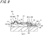
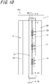
- a thermal head X5 according to a fifth embodiment will be described with reference to FIGS. 8 to 11 .
- the wiring board 22 is indicated by a dotted line.
- the thermal head X5 includes the heatsink 1, the head base 3, the wiring board 22, and an FPC 5.
- the heatsink 1 includes the base portion 1a, the first convex portion 1b, and the second convex portion 1c.
- the head base 3 does not include the IC-IC connection electrode 26, the ground electrode 4, and the drive IC 11, and is different from the thermal head X1 in wiring patterns of various electrodes.
- the wiring board 22 is disposed on the heatsink 1, and is disposed adjacent to the head base 3 in a sub scanning direction.
- the wiring board 22 is configured so that the drive ICs 11 and the wiring patterns 24 are disposed on a glass epoxy substrate or a polyimide substrate.
- Each drive IC 11 includes a pair of metal wires 35, in which one of the wires 35 is electrically connected to the conductive member 23 of the head base 3. Further, the other one of the wires 35 is electrically connected to the wiring pattern 24 of the wiring board 22.
- the wiring board 22 and the head base 3 are electrically connected to each other.
- the wires 35 that electrically connects the conductive member 23 on the head base 3, and the wiring pattern 24 on the wiring board 22 are configured by a fine line made of a metallic material such as gold (Au).
- the wire 35 is formed to stride over a gap between the head base 3 and the wiring board 22, and electrically connects the head base 3 and the wiring board 22 by a known wire bonding method in the related art.
- the wire 35 is used as the conductive member.
- the FPC 5 is electrically connected to the wiring board 22 through the conductive member 23.
- the electric connection between the FPC 5 and the wiring board 22 is performed by the above-described solder connection or AFC connection.
- a flexible print wiring board may be used, for example.
- a reinforcing plate (not shown) formed of resin such as phenol resin, polyimide resin or glass epoxy resin may be disposed between the flexible print wiring board and the heatsink 1.
- the wiring board 22 and the head base 3 are disposed in a state of being spaced from each other, and the plural drive ICs 11 are disposed on the head base 3 side of the wiring board 22.
- the plural wires 35 are arranged side by side in the main scanning direction.
- the first convex portion 1b and the second convex portion 1c of the heatsink 1 are disposed side by side with the plural wires 35 in the main scanning direction.
- the wiring board 22 and the head base 3 may be disposed in a state of being in contact with each other. Further, the connector 31 (see FIG. 1 ) may be connected to the wiring board 22.
- the protective member 12 is disposed so as to cover a space 34 between the wiring board 22 and the head base 3, the plural wires 35, a part of the first convex portion 1b, and a part of the second convex portion 1c.
- the protective member 12 since the first convex portion 1b and the second convex portion 1c are disposed in the opposite end portions in the main scanning direction, when the protective member 12 is applied onto the wires 35, it is possible to reduce a possibility that the protective member 12 flows out to protrude from the heatsink 1. Thus, it is possible to reduce a possibility that a poor appearance of the thermal head X5 is caused, and to enhance a yield rate of the thermal head X5.
- first convex portion 1b and the second convex portion 1c can suppress the outflow of the protective member 12, it is possible to reduce a possibility that the amount of the protective member 12 disposed on the wires 35 is insufficient to cause a low sealing height. Thus, it is possible to reduce a possibility that the drive ICs 11 or the wires 35 are exposed, and to obtain the thermal head X5 with enhanced reliability.
- the protective member 12 is easily insufficient, it is possible to suppress the outflow of the protective member 12, and to reduce a possibility that the protective member 12 becomes insufficient.
- a material of forming the protective member 12 the same material as that of the covering member 29 (see FIG. 2 ) may be used, for example.
- the first convex portion 1b is disposed in a state of being in contact with a side surface of the head base 3 and a side surface of the wiring board 22.
- the first convex portion 1b may be used as a positioning member.
- the second convex portion 1c is disposed on a side opposite to the first convex portion 1b across the wires 35.
- the first convex portion 1b is disposed on one end portion of the head base 3 and the wiring board 22 in the main scanning direction
- the second convex portion 1c is disposed in the other end portion of the head base 3 and the wiring board 22 in the main scanning direction.
- the first convex portion 1b and the second convex portion 1c sandwich a bonding area between the head base 3 and the wiring board 22, which is an area where the protective member 12 is applied, in the main scanning direction.
- the protective member 12 flows out, and as a result, it is not necessary to provide an extra amount of the protective member 12.
- the second convex portion 1c is disposed in a state of being spaced from the side surface of the head base 3 and the side surface of the wiring board 22.
- the protective member 12 between the side surface of the head base 3 and the side surface of the wiring board 22, and the second convex portion 1c.
- first convex portion 1b is disposed in a state of being in contact with the side surface of the head base 3 and the side surface of the wiring board 22, and the second convex portion 1c is disposed in a state of being spaced from the side surface of the head base 3 and the side surface of the wiring board 22.
- the heights of the first convex portion 1b and the second convex potion 1c are higher than the height of the wiring board 22. Therefore, when the protective film 12 is applied, it is possible to effectively suppress the outflow of the protective member 12.
- the heights of the first convex portion 1b and the second convex potion 1c are equal to or higher than the height of the head base 3. As shown in FIG. 9 , the height of the head base 3 is higher than the height of the wiring board 22. Thus, an area around the drive IC 11 which is an area where the protective member 12 is applied is surrounded by the head base 3, the first convex portion 1b, and the second convex potion 1c. Thus, it is possible to further reduce a possibility that the protective member 12 flows out.
- the protective member 12 is applied up to an upper surface 1d of the first convex portion 1b and an upper surface 1d of the second convex portion 1c.
- the protective member 12 is applied up to an upper surface 1d of the first convex portion 1b and an upper surface 1d of the second convex portion 1c.
- the first convex portion 1b may be spaced from the side surface of the head base 3 and the side surface of the wiring board 22.
- the second convex portion 1c may not be provided.
- the first convex portion 1b and the second convex potion 1c may be disposed in a state of being in contact with the side surface of the head base 3 and the side surface of the wiring board 22.
- a thermal head X5a which is a modified example of the thermal head X5 will be described with reference to FIG. 12 .
- the thermal head X5a has a configuration in which the length of the wiring board 22 in the main scanning direction is shorter than the length of the head base 3 in the main scanning direction. Further, the first convex portion 1b and the second convex potion 1c are disposed in an area 36 formed between the head base 3 and the wiring board 22. Thus, it is possible to reduce the length of the thermal head X5a in the main scanning direction, to thereby achieve miniaturization in the main scanning direction.
- first convex portion 1b and the second convex potion 1c are disposed in a state of being in contact with the wiring board 22.
- the thermal head X5a in which the drive ICs 11 are disposed on the wiring board 22 the heat is transferred from the drive ICs 11 to the wiring board 22, and the heat is radiated from the wiring board 22 to the heatsink 1 through the protective member 12.
- first convex portion 1b and the second convex potion 1c are used for positioning of the head base 3, and fixedly support the head base 3. That is, the first convex portion 1b and the second convex potion 1c are in contact with the side surface 7e of the substrate 7 to fixedly support the head base 3.
- the thermal head X5a may be provided with only the first convex portion 1b, or may be provided with only the second convex portion 1c.
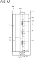
- a thermal head X6 according to a sixth embodiment will be described with reference to FIGS. 13 and 14 .
- the thermal head X6 is different from the thermal heads X1 to X5a in that a first concave portion 1e instead of the second convex portion 1c is provided.
- Other configurations are the same.
- the wiring board 22 is indicated by a dotted line.
- the heatsink 1 includes the base portion 1a, the first convex portion 1b, and the first concave portion 1e.
- the first concave portion 1e is recessed from a front surface of the heatsink 1. Further, the first concave portion 1e is disposed on a side opposite to the first convex portion 1b in the main scanning direction. In other words, the first convex portion 1b is disposed in one end portion of the head base 3 and the wiring board 22 in the main scanning direction, and the first concave portion 1e is disposed in the other end portion of the head base 3 and the wiring board 22 in the main scanning direction.
- first concave portion 1e may be provided instead of the first convex portion 1b, and the first concave portion 1e and a second concave portion (not shown, and not included in the scope of claimed matter) may be provided instead of the first convex portion 1b and the second convex portion 1c.
- a thermal head X7 according to a seventh embodiment will be described with reference to FIG. 15 .
- the thermal head X7 has a configuration in which the first convex portion 1b and the second convex portion 1c are disposed under the accommodating portion 10 of the connector 31.
- the accommodating portion 10 is disposed on the upper surfaces of the first convex portion 1b and the second convex portion 1c.
- a configuration in which the first convex portion 1b and the second convex portion 1c support the connector 31 from below is obtained.
- the first convex portion 1b and the second convex portion 1c can retain the connector 31.
- first convex portion 1b may be disposed in the vicinity of the bonding area between the wiring board 22 and the connector 31. In this case, similarly, the first convex portion 1b can efficiently radiate heat generated due to electric resistance of the wiring board 22 and the connector 31 to the heatsink 1.
- the protective member 12 is disposed in an area surrounded by the first convex portion 1b, the second convex portion 1c, and the accommodating portion 10.
- the protective member 12 is disposed in an area surrounded by the first convex portion 1b, the second convex portion 1c, and the accommodating portion 10.
- a thermal head X8 according to an eighth embodiment will be described with reference to FIG. 16 .
- the thermal head X8 includes the head base 3, the wires 35, the wiring board 22, the FPC 5, and the protective member 12.
- the head base 3 and the wiring board 22 are electrically connected to each other by the wires 35, and the wiring board 22 is electrically connected to an external device through the FPC 5.
- the FPC 5 and the wiring board 22 are electrically connected to each other through the conductive members 23 (not shown), and in the present embodiment, the conductive members include the wires 35 and the conductive members 23.
- the heatsink 1 includes the first convex portion 1b and the second convex portion 1c, the first convex portion 1b and the second convex portion 1c are disposed adjacent to the wiring board 22. Further, the first convex portion 1b and the second convex portion 1c are disposed adjacent to the FPC 5.
- the wiring board 22 is positioned by the first convex portion 1b and the second convex portion 1c.
- the FPC 5 is positioned by the first convex portion 1b and the second convex portion 1c.
- the protective member 12 is disposed so as to cover the wires 35. Further, the protective member 12 that covers the wires 35 is in contact with the heatsink 1. Further, the protective member 12 is disposed so as to cover an end portion of the FPC 5, and a part of the protective member 12 is in contact with the first convex portion 1b and the second convex portion 1c.
- the protective members 12 may be disposed as separated members so as to cover the wires 35 and the conductive members 23, and a part of the protective member 12 may be in contact with the heatsink 1. In this case, similarly, it is possible to efficiently radiate heat generated by the wires 35 or heat generated by the conductive members 23 through the respective protective members 12.
- the thermal printer Z1 using the thermal head X1 according to the first embodiment is shown, but the invention is not limited thereto, and the thermal heads X2 to X8 may be used in the thermal printer Z1. Further, the thermal heads X1 to X8 according to the plural embodiments may be combined.
- the protruding portion 13b is formed in the heat storage layer 13 and the electrical resistance layer 15 is formed on the protruding portion 13b, but the invention is not limited thereto.
- the protruding portion 13b may not be formed in the heat storage layer 13, and instead, the heat generating portion 9 of the electrical resistance layer 15 may be disposed on the base portion 13a of the heat storage layer 13. Further, the heat storage layer 13 may be disposed over an overall area of the upper surface of the substrate 7.
- the common electrode 17 and the individual electrodes 19 are formed on the electrical resistance layer 15, but as long as both the common electrode 17 and the individual electrodes 19 are connected to the heat generating portions 9 (electric resistance bodies), the invention is not limited thereto.
- the heat generating portion 9 may be formed by forming the common electrode 17 and the individual electrodes 19 on the heat storage layer 13 and forming the electrical resistance layer 15 only in an area between the common electrode 17 and the individual electrodes 19.
- the invention may be applied to a thick film head in which the thick-film heat generating portions 9 are provided by forming the electrical resistance layer 15 to be thick after various electrodes are patterned.
- the present technique may be applied to an edge head in which the heat generating portions 9 are formed on an edge surface of the substrate 7.
Landscapes
- Physics & Mathematics (AREA)
- Geometry (AREA)
- Electronic Switches (AREA)
Claims (12)
- Thermokopf, aufweisend:ein Substrat (7),eine Mehrzahl von wärmeerzeugenden Abschnitten (9), die auf dem Substrat (7) angeordnet sind,eine Elektrode (21), die auf dem Substrat (7) angeordnet ist und elektrisch mit den wärmeerzeugenden Abschnitten (9) verbunden ist,einen Verbinder (31), der einen Verbinderstift (8) und einen Aufnahmeabschnitt (10) aufweist, der den Verbinderstift (8) aufnimmt,ein leitfähiges Element (23), das die Elektrode (21) und den Verbinderstift (8) elektrisch miteinander verbindet,ein Schutzelement (12), das mit dem leitfähigen Element (23) in Kontakt ist und das leitfähige Element (23) schützt, undeinen Kühlkörper (1), der unter dem Substrat (7) angeordnet ist,wobei das Schutzelement (12) auch mit dem Kühlkörper in Kontakt ist,wobei der Kühlkörper (1) einen ersten konvexen Abschnitt (1b) aufweist, der nach oben hervorsteht,wobei der erste konvexe Abschnitt (1b) und der Aufnahmeabschnitt (10) benachbart zueinander angeordnet sind,wobei das Schutzelement (12) zwischen dem ersten konvexen Abschnitt (1b) und dem Aufnahmeabschnitt (10) angeordnet ist,wobei das Schutzelement (12) mit dem ersten konvexen Abschnitt (1b) in Kontakt ist.
- Thermokopf gemäß Anspruch 1,wobei der Aufnahmeabschnitt (10) über dem Kühlkörper (1) angeordnet ist, um von dem Kühlkörper (1) in einem vorbestimmten Abstand angeordnet zu sein, unddas Schutzelement (12) zwischen dem Aufnahmeabschnitt (10) und dem Kühlkörper (1) angeordnet ist.
- Thermokopf gemäß Anspruch 2,wobei ein Teil des Schutzelements (12), der zwischen dem Aufnahmeabschnitt (10) und dem Kühlkörper (1) angeordnet ist, ein oberes Ende (12a), das mit dem Aufnahmeabschnitt (10) in Kontakt ist, und ein unteres Ende (12b), das mit dem Kühlkörper (1) in Kontakt ist, aufweist, undin einer Draufsicht auf das Substrat (7) ein Rand des unteren Endes (12b) weiter von dem Substrat (7) entfernt als ein Rand des oberen Endes (12a) angeordnet ist.
- Thermokopf gemäß irgendeinem der Ansprüche 1 bis 3,wobei der Kühlkörper (1) einen zweiten konvexen Abschnitt (1c) aufweist, der nach oben hervorsteht,der Aufnahmeabschnitt (10) zwischen dem ersten konvexen Abschnitt (1b) und dem zweiten konvexen Abschnitt (1c) angeordnet ist, undder zweite konvexe Abschnitt (1c) und der Aufnahmeabschnitt (10) in Kontakt miteinander sind.
- Thermokopf gemäß irgendeinem der Ansprüche 1 bis 3,wobei der Kühlkörper (1) einen zweiten konvexen Abschnitt (1c) aufweist, der nach oben hervorsteht,der Aufnahmeabschnitt (10) zwischen dem ersten konvexen Abschnitt (1b) und dem zweiten konvexen Abschnitt (1c) angeordnet ist, unddas Schutzelement (12) auch zwischen dem zweiten konvexen Abschnitt (1c) und dem Aufnahmeabschnitt (10) angeordnet ist.
- Thermokopf gemäß Anspruch 4 oder 5,
wobei ein Abstand zwischen dem ersten konvexen Abschnitt (1b) und dem Aufnahmeabschnitt (10) von einem Abstand zwischen dem zweiten konvexen Abschnitt (1c) und dem Aufnahmeabschnitt (10) verschieden ist. - Thermokopf gemäß irgendeinem der Ansprüche 4 bis 6,
wobei das Substrat (7) und mindestens einer von dem ersten konvexen Abschnitt (1b) und dem zweiten konvexen Abschnitt (1c) miteinander in Kontakt sind. - Thermokopf gemäß Anspruch 1, ferner aufweisend:eine Verdrahtungsplatte (22), die benachbart zu dem Substrat (7) in einer Nebenscanrichtung auf dem Kühlkörper (1) angeordnet und elektrisch mit dem Substrat (7) verbunden ist,wobei die Verdrahtungsplatte (22) eine Mehrzahl von Verbindungselementen (35) in einer Hauptscanrichtung aufweist, in der die Mehrzahl von Verbindungselementen (35) mit dem Schutzelement (12) bedeckt sind, undder erste konvexe Abschnitt (1b) in der Hauptscanrichtung Seite an Seite mit den Verbindungselementen (35) angeordnet ist.
- Thermokopf gemäß Anspruch 8,
wobei der erste konvexe Abschnitt (1b) in einem Zustand angeordnet ist, in dem er mit dem Substrat (7) in Kontakt ist. - Thermokopf gemäß Anspruch 8 oder 9,wobei der Kühlkörper (1) einen zweiten konvexen Abschnitt (1c) aufweist, der nach oben hervorsteht, undder zweite konvexe Abschnitt (1c) auf einer dem ersten konvexen Abschnitt (1b) gegenüberliegenden Seite über die Verbindungselemente (35) angeordnet ist.
- Thermokopf gemäß Anspruch 10,
wobei der zweite konvexe Abschnitt (1c) in einem Zustand angeordnet ist, in dem er von dem Substrat (7) im Abstand angeordnet ist. - Thermodrucker, aufweisend:den Thermokopf gemäß irgendeinem der Ansprüche 1 bis 11,einen Transportmechanismus (40), der ein Aufzeichnungsmedium (P) auf die wärmeerzeugenden Abschnitte (9) transportiert, undeine Druckwalze (50), die das Aufzeichnungsmedium (P) auf die wärmeerzeugenden Abschnitte (9) drückt.
Applications Claiming Priority (3)
| Application Number | Priority Date | Filing Date | Title |
|---|---|---|---|
| JP2013037397 | 2013-02-27 | ||
| JP2013204368 | 2013-09-30 | ||
| PCT/JP2014/053993 WO2014132870A1 (ja) | 2013-02-27 | 2014-02-20 | サーマルヘッドおよびサーマルプリンタ |
Publications (3)
| Publication Number | Publication Date |
|---|---|
| EP2962857A1 EP2962857A1 (de) | 2016-01-06 |
| EP2962857A4 EP2962857A4 (de) | 2017-03-01 |
| EP2962857B1 true EP2962857B1 (de) | 2022-07-27 |
Family
ID=51428141
Family Applications (1)
| Application Number | Title | Priority Date | Filing Date |
|---|---|---|---|
| EP14757409.9A Active EP2962857B1 (de) | 2013-02-27 | 2014-02-20 | Thermodruckkopf und thermodrucker |
Country Status (5)
| Country | Link |
|---|---|
| US (1) | US9457588B2 (de) |
| EP (1) | EP2962857B1 (de) |
| JP (1) | JP6018288B2 (de) |
| CN (1) | CN105026165B (de) |
| WO (1) | WO2014132870A1 (de) |
Families Citing this family (9)
| Publication number | Priority date | Publication date | Assignee | Title |
|---|---|---|---|---|
| JP6401066B2 (ja) * | 2015-01-27 | 2018-10-03 | 京セラ株式会社 | サーマルヘッドおよびこれを備えるサーマルプリンタ |
| JP6401078B2 (ja) * | 2015-02-26 | 2018-10-03 | 京セラ株式会社 | サーマルヘッドおよびこれを備えるサーマルプリンタ |
| JP6676369B2 (ja) * | 2015-12-25 | 2020-04-08 | ローム株式会社 | サーマルプリントヘッドおよびサーマルプリンタ |
| JP6781125B2 (ja) * | 2017-09-13 | 2020-11-04 | アオイ電子株式会社 | サーマルヘッド |
| JP2019177604A (ja) * | 2018-03-30 | 2019-10-17 | ブラザー工業株式会社 | ヘッド制御回路基板、及び印刷装置 |
| WO2020241581A1 (ja) * | 2019-05-27 | 2020-12-03 | ローム株式会社 | サーマルプリントヘッド |
| JP7329423B2 (ja) * | 2019-11-18 | 2023-08-18 | ローム株式会社 | サーマルプリントヘッドおよびサーマルプリンタ |
| CN110884260A (zh) * | 2019-12-28 | 2020-03-17 | 厦门芯瓷科技有限公司 | 一种热敏打印头及其制造方法 |
| JPWO2024014066A1 (de) * | 2022-07-11 | 2024-01-18 |
Family Cites Families (14)
| Publication number | Priority date | Publication date | Assignee | Title |
|---|---|---|---|---|
| JPS63179764A (ja) * | 1987-01-22 | 1988-07-23 | Konica Corp | 感熱記録ヘツド |
| JP2793230B2 (ja) * | 1989-03-01 | 1998-09-03 | 京セラ株式会社 | サーマルヘッド |
| JPH02248257A (ja) | 1989-03-22 | 1990-10-04 | Matsushita Electric Ind Co Ltd | サーマルヘッド |
| JPH0664187A (ja) * | 1992-08-13 | 1994-03-08 | Fuji Xerox Co Ltd | インクジェット記録装置及びヘッドユニット |
| JPH09150540A (ja) * | 1995-11-30 | 1997-06-10 | Kyocera Corp | サーマルヘッド |
| DE69734152T2 (de) * | 1996-12-19 | 2006-07-13 | Tdk Corp. | Thermokopf und verfahren zu seiner herstellung |
| JP2001113741A (ja) | 1999-10-19 | 2001-04-24 | Rohm Co Ltd | サーマルプリントヘッドおよびその製造方法 |
| JP3563734B2 (ja) * | 2002-10-29 | 2004-09-08 | ローム株式会社 | サーマルプリントヘッド装置 |
| EP1547777B1 (de) * | 2003-12-26 | 2011-06-08 | Canon Kabushiki Kaisha | Tintenstrahlkopf, Ansteuerungsverfahren des Kopfes, und Tintenstrahldrucker |
| CN101808829B (zh) * | 2007-09-28 | 2012-03-07 | 京瓷株式会社 | 记录头以及具备该记录头的记录装置 |
| CN103269862B (zh) * | 2010-12-25 | 2015-08-05 | 京瓷株式会社 | 热敏头以及具备该热敏头的热敏打印机 |
| US9061520B2 (en) * | 2011-01-25 | 2015-06-23 | Kyocera Corporation | Thermal head and thermal printer including the same |
| JP5836825B2 (ja) * | 2011-02-24 | 2015-12-24 | 京セラ株式会社 | サーマルヘッドおよびこれを備えるサーマルプリンタ |
| JP5937309B2 (ja) * | 2011-07-07 | 2016-06-22 | 京セラ株式会社 | サーマルヘッドおよびこれを備えるサーマルプリンタ |
-
2014
- 2014-02-20 EP EP14757409.9A patent/EP2962857B1/de active Active
- 2014-02-20 CN CN201480011004.8A patent/CN105026165B/zh active Active
- 2014-02-20 US US14/770,321 patent/US9457588B2/en active Active
- 2014-02-20 JP JP2015502888A patent/JP6018288B2/ja active Active
- 2014-02-20 WO PCT/JP2014/053993 patent/WO2014132870A1/ja not_active Ceased
Also Published As
| Publication number | Publication date |
|---|---|
| CN105026165A (zh) | 2015-11-04 |
| US20160001573A1 (en) | 2016-01-07 |
| JPWO2014132870A1 (ja) | 2017-02-02 |
| WO2014132870A1 (ja) | 2014-09-04 |
| JP6018288B2 (ja) | 2016-11-02 |
| EP2962857A4 (de) | 2017-03-01 |
| EP2962857A1 (de) | 2016-01-06 |
| US9457588B2 (en) | 2016-10-04 |
| CN105026165B (zh) | 2017-06-09 |
Similar Documents
| Publication | Publication Date | Title |
|---|---|---|
| EP2962857B1 (de) | Thermodruckkopf und thermodrucker | |
| CN105916691B (zh) | 热敏头以及热敏式打印机 | |
| JP6219408B2 (ja) | サーマルヘッドおよびサーマルプリンタ | |
| JP6001465B2 (ja) | サーマルヘッドおよびこれを備えるサーマルプリンタ | |
| CN107848311B (zh) | 热敏头及热敏打印机 | |
| CN115298037B (zh) | 热敏头以及热敏打印机 | |
| CN115315356B (zh) | 热敏头以及热敏打印机 | |
| US9844950B2 (en) | Thermal head and thermal printer provided with same | |
| JP6208561B2 (ja) | サーマルヘッドおよびサーマルプリンタ | |
| JP6050562B2 (ja) | サーマルヘッドおよびサーマルプリンタ | |
| CN113677535A (zh) | 热敏头以及热敏打印机 | |
| CN106536206B (zh) | 热敏头以及热敏打印机 | |
| CN108025558B (zh) | 热敏头以及热敏打印机 | |
| JP6110198B2 (ja) | サーマルヘッドおよびサーマルプリンタ | |
| JP6401066B2 (ja) | サーマルヘッドおよびこれを備えるサーマルプリンタ | |
| JP6352799B2 (ja) | サーマルヘッドおよびサーマルプリンタ | |
| JP6075626B2 (ja) | サーマルヘッドおよびサーマルプリンタ | |
| JP6204084B2 (ja) | サーマルヘッドおよびサーマルプリンタ | |
| JP2015182240A (ja) | サーマルヘッドおよびサーマルプリンタ | |
| JP6081888B2 (ja) | サーマルヘッドおよびこれを備えるサーマルプリンタ | |
| JP2015044389A (ja) | サーマルヘッドおよびサーマルプリンタ | |
| JPWO2017057364A1 (ja) | サーマルヘッドおよびサーマルプリンタ | |
| JP2016055613A (ja) | サーマルヘッドおよびサーマルプリンタ |
Legal Events
| Date | Code | Title | Description |
|---|---|---|---|
| PUAI | Public reference made under article 153(3) epc to a published international application that has entered the european phase |
Free format text: ORIGINAL CODE: 0009012 |
|
| 17P | Request for examination filed |
Effective date: 20150826 |
|
| AK | Designated contracting states |
Kind code of ref document: A1 Designated state(s): AL AT BE BG CH CY CZ DE DK EE ES FI FR GB GR HR HU IE IS IT LI LT LU LV MC MK MT NL NO PL PT RO RS SE SI SK SM TR |
|
| AX | Request for extension of the european patent |
Extension state: BA ME |
|
| DAX | Request for extension of the european patent (deleted) | ||
| A4 | Supplementary search report drawn up and despatched |
Effective date: 20170131 |
|
| RIC1 | Information provided on ipc code assigned before grant |
Ipc: B41J 2/335 20060101AFI20170125BHEP Ipc: B41J 2/32 20060101ALI20170125BHEP |
|
| RIN1 | Information on inventor provided before grant (corrected) |
Inventor name: YONETA, MASASHI |
|
| STAA | Information on the status of an ep patent application or granted ep patent |
Free format text: STATUS: EXAMINATION IS IN PROGRESS |
|
| 17Q | First examination report despatched |
Effective date: 20210301 |
|
| GRAP | Despatch of communication of intention to grant a patent |
Free format text: ORIGINAL CODE: EPIDOSNIGR1 |
|
| STAA | Information on the status of an ep patent application or granted ep patent |
Free format text: STATUS: GRANT OF PATENT IS INTENDED |
|
| INTG | Intention to grant announced |
Effective date: 20220223 |
|
| RAP3 | Party data changed (applicant data changed or rights of an application transferred) |
Owner name: KYOCERA CORPORATION |
|
| GRAS | Grant fee paid |
Free format text: ORIGINAL CODE: EPIDOSNIGR3 |
|
| GRAA | (expected) grant |
Free format text: ORIGINAL CODE: 0009210 |
|
| STAA | Information on the status of an ep patent application or granted ep patent |
Free format text: STATUS: THE PATENT HAS BEEN GRANTED |
|
| AK | Designated contracting states |
Kind code of ref document: B1 Designated state(s): AL AT BE BG CH CY CZ DE DK EE ES FI FR GB GR HR HU IE IS IT LI LT LU LV MC MK MT NL NO PL PT RO RS SE SI SK SM TR |
|
| REG | Reference to a national code |
Ref country code: CH Ref legal event code: EP |
|
| REG | Reference to a national code |
Ref country code: AT Ref legal event code: REF Ref document number: 1506828 Country of ref document: AT Kind code of ref document: T Effective date: 20220815 |
|
| REG | Reference to a national code |
Ref country code: DE Ref legal event code: R096 Ref document number: 602014084405 Country of ref document: DE |
|
| REG | Reference to a national code |
Ref country code: IE Ref legal event code: FG4D |
|
| REG | Reference to a national code |
Ref country code: LT Ref legal event code: MG9D |
|
| REG | Reference to a national code |
Ref country code: NL Ref legal event code: MP Effective date: 20220727 |
|
| PG25 | Lapsed in a contracting state [announced via postgrant information from national office to epo] |
Ref country code: SE Free format text: LAPSE BECAUSE OF FAILURE TO SUBMIT A TRANSLATION OF THE DESCRIPTION OR TO PAY THE FEE WITHIN THE PRESCRIBED TIME-LIMIT Effective date: 20220727 Ref country code: RS Free format text: LAPSE BECAUSE OF FAILURE TO SUBMIT A TRANSLATION OF THE DESCRIPTION OR TO PAY THE FEE WITHIN THE PRESCRIBED TIME-LIMIT Effective date: 20220727 Ref country code: PT Free format text: LAPSE BECAUSE OF FAILURE TO SUBMIT A TRANSLATION OF THE DESCRIPTION OR TO PAY THE FEE WITHIN THE PRESCRIBED TIME-LIMIT Effective date: 20221128 Ref country code: NO Free format text: LAPSE BECAUSE OF FAILURE TO SUBMIT A TRANSLATION OF THE DESCRIPTION OR TO PAY THE FEE WITHIN THE PRESCRIBED TIME-LIMIT Effective date: 20221027 Ref country code: NL Free format text: LAPSE BECAUSE OF FAILURE TO SUBMIT A TRANSLATION OF THE DESCRIPTION OR TO PAY THE FEE WITHIN THE PRESCRIBED TIME-LIMIT Effective date: 20220727 Ref country code: LV Free format text: LAPSE BECAUSE OF FAILURE TO SUBMIT A TRANSLATION OF THE DESCRIPTION OR TO PAY THE FEE WITHIN THE PRESCRIBED TIME-LIMIT Effective date: 20220727 Ref country code: LT Free format text: LAPSE BECAUSE OF FAILURE TO SUBMIT A TRANSLATION OF THE DESCRIPTION OR TO PAY THE FEE WITHIN THE PRESCRIBED TIME-LIMIT Effective date: 20220727 Ref country code: FI Free format text: LAPSE BECAUSE OF FAILURE TO SUBMIT A TRANSLATION OF THE DESCRIPTION OR TO PAY THE FEE WITHIN THE PRESCRIBED TIME-LIMIT Effective date: 20220727 Ref country code: ES Free format text: LAPSE BECAUSE OF FAILURE TO SUBMIT A TRANSLATION OF THE DESCRIPTION OR TO PAY THE FEE WITHIN THE PRESCRIBED TIME-LIMIT Effective date: 20220727 |
|
| REG | Reference to a national code |
Ref country code: AT Ref legal event code: MK05 Ref document number: 1506828 Country of ref document: AT Kind code of ref document: T Effective date: 20220727 |
|
| PG25 | Lapsed in a contracting state [announced via postgrant information from national office to epo] |
Ref country code: PL Free format text: LAPSE BECAUSE OF FAILURE TO SUBMIT A TRANSLATION OF THE DESCRIPTION OR TO PAY THE FEE WITHIN THE PRESCRIBED TIME-LIMIT Effective date: 20220727 Ref country code: IS Free format text: LAPSE BECAUSE OF FAILURE TO SUBMIT A TRANSLATION OF THE DESCRIPTION OR TO PAY THE FEE WITHIN THE PRESCRIBED TIME-LIMIT Effective date: 20221127 Ref country code: HR Free format text: LAPSE BECAUSE OF FAILURE TO SUBMIT A TRANSLATION OF THE DESCRIPTION OR TO PAY THE FEE WITHIN THE PRESCRIBED TIME-LIMIT Effective date: 20220727 Ref country code: GR Free format text: LAPSE BECAUSE OF FAILURE TO SUBMIT A TRANSLATION OF THE DESCRIPTION OR TO PAY THE FEE WITHIN THE PRESCRIBED TIME-LIMIT Effective date: 20221028 |
|
| PG25 | Lapsed in a contracting state [announced via postgrant information from national office to epo] |
Ref country code: SM Free format text: LAPSE BECAUSE OF FAILURE TO SUBMIT A TRANSLATION OF THE DESCRIPTION OR TO PAY THE FEE WITHIN THE PRESCRIBED TIME-LIMIT Effective date: 20220727 Ref country code: RO Free format text: LAPSE BECAUSE OF FAILURE TO SUBMIT A TRANSLATION OF THE DESCRIPTION OR TO PAY THE FEE WITHIN THE PRESCRIBED TIME-LIMIT Effective date: 20220727 Ref country code: DK Free format text: LAPSE BECAUSE OF FAILURE TO SUBMIT A TRANSLATION OF THE DESCRIPTION OR TO PAY THE FEE WITHIN THE PRESCRIBED TIME-LIMIT Effective date: 20220727 Ref country code: CZ Free format text: LAPSE BECAUSE OF FAILURE TO SUBMIT A TRANSLATION OF THE DESCRIPTION OR TO PAY THE FEE WITHIN THE PRESCRIBED TIME-LIMIT Effective date: 20220727 Ref country code: AT Free format text: LAPSE BECAUSE OF FAILURE TO SUBMIT A TRANSLATION OF THE DESCRIPTION OR TO PAY THE FEE WITHIN THE PRESCRIBED TIME-LIMIT Effective date: 20220727 |
|
| REG | Reference to a national code |
Ref country code: DE Ref legal event code: R097 Ref document number: 602014084405 Country of ref document: DE |
|
| PG25 | Lapsed in a contracting state [announced via postgrant information from national office to epo] |
Ref country code: SK Free format text: LAPSE BECAUSE OF FAILURE TO SUBMIT A TRANSLATION OF THE DESCRIPTION OR TO PAY THE FEE WITHIN THE PRESCRIBED TIME-LIMIT Effective date: 20220727 Ref country code: EE Free format text: LAPSE BECAUSE OF FAILURE TO SUBMIT A TRANSLATION OF THE DESCRIPTION OR TO PAY THE FEE WITHIN THE PRESCRIBED TIME-LIMIT Effective date: 20220727 |
|
| PLBE | No opposition filed within time limit |
Free format text: ORIGINAL CODE: 0009261 |
|
| STAA | Information on the status of an ep patent application or granted ep patent |
Free format text: STATUS: NO OPPOSITION FILED WITHIN TIME LIMIT |
|
| P01 | Opt-out of the competence of the unified patent court (upc) registered |
Effective date: 20230508 |
|
| PG25 | Lapsed in a contracting state [announced via postgrant information from national office to epo] |
Ref country code: AL Free format text: LAPSE BECAUSE OF FAILURE TO SUBMIT A TRANSLATION OF THE DESCRIPTION OR TO PAY THE FEE WITHIN THE PRESCRIBED TIME-LIMIT Effective date: 20220727 |
|
| 26N | No opposition filed |
Effective date: 20230502 |
|
| PG25 | Lapsed in a contracting state [announced via postgrant information from national office to epo] |
Ref country code: SI Free format text: LAPSE BECAUSE OF FAILURE TO SUBMIT A TRANSLATION OF THE DESCRIPTION OR TO PAY THE FEE WITHIN THE PRESCRIBED TIME-LIMIT Effective date: 20220727 |
|
| PG25 | Lapsed in a contracting state [announced via postgrant information from national office to epo] |
Ref country code: MC Free format text: LAPSE BECAUSE OF FAILURE TO SUBMIT A TRANSLATION OF THE DESCRIPTION OR TO PAY THE FEE WITHIN THE PRESCRIBED TIME-LIMIT Effective date: 20220727 |
|
| REG | Reference to a national code |
Ref country code: CH Ref legal event code: PL |
|
| REG | Reference to a national code |
Ref country code: BE Ref legal event code: MM Effective date: 20230228 |
|
| PG25 | Lapsed in a contracting state [announced via postgrant information from national office to epo] |
Ref country code: LU Free format text: LAPSE BECAUSE OF NON-PAYMENT OF DUE FEES Effective date: 20230220 Ref country code: LI Free format text: LAPSE BECAUSE OF NON-PAYMENT OF DUE FEES Effective date: 20230228 Ref country code: CH Free format text: LAPSE BECAUSE OF NON-PAYMENT OF DUE FEES Effective date: 20230228 |
|
| REG | Reference to a national code |
Ref country code: IE Ref legal event code: MM4A |
|
| PG25 | Lapsed in a contracting state [announced via postgrant information from national office to epo] |
Ref country code: IE Free format text: LAPSE BECAUSE OF NON-PAYMENT OF DUE FEES Effective date: 20230220 |
|
| PG25 | Lapsed in a contracting state [announced via postgrant information from national office to epo] |
Ref country code: BE Free format text: LAPSE BECAUSE OF NON-PAYMENT OF DUE FEES Effective date: 20230228 |
|
| PG25 | Lapsed in a contracting state [announced via postgrant information from national office to epo] |
Ref country code: IT Free format text: LAPSE BECAUSE OF FAILURE TO SUBMIT A TRANSLATION OF THE DESCRIPTION OR TO PAY THE FEE WITHIN THE PRESCRIBED TIME-LIMIT Effective date: 20220727 |
|
| PG25 | Lapsed in a contracting state [announced via postgrant information from national office to epo] |
Ref country code: BG Free format text: LAPSE BECAUSE OF FAILURE TO SUBMIT A TRANSLATION OF THE DESCRIPTION OR TO PAY THE FEE WITHIN THE PRESCRIBED TIME-LIMIT Effective date: 20220727 |
|
| PG25 | Lapsed in a contracting state [announced via postgrant information from national office to epo] |
Ref country code: BG Free format text: LAPSE BECAUSE OF FAILURE TO SUBMIT A TRANSLATION OF THE DESCRIPTION OR TO PAY THE FEE WITHIN THE PRESCRIBED TIME-LIMIT Effective date: 20220727 |
|
| PGFP | Annual fee paid to national office [announced via postgrant information from national office to epo] |
Ref country code: DE Payment date: 20241231 Year of fee payment: 12 |
|
| PGFP | Annual fee paid to national office [announced via postgrant information from national office to epo] |
Ref country code: GB Payment date: 20250102 Year of fee payment: 12 |
|
| PG25 | Lapsed in a contracting state [announced via postgrant information from national office to epo] |
Ref country code: CY Free format text: LAPSE BECAUSE OF FAILURE TO SUBMIT A TRANSLATION OF THE DESCRIPTION OR TO PAY THE FEE WITHIN THE PRESCRIBED TIME-LIMIT; INVALID AB INITIO Effective date: 20140220 |
|
| PG25 | Lapsed in a contracting state [announced via postgrant information from national office to epo] |
Ref country code: HU Free format text: LAPSE BECAUSE OF FAILURE TO SUBMIT A TRANSLATION OF THE DESCRIPTION OR TO PAY THE FEE WITHIN THE PRESCRIBED TIME-LIMIT; INVALID AB INITIO Effective date: 20140220 |
|
| PG25 | Lapsed in a contracting state [announced via postgrant information from national office to epo] |
Ref country code: TR Free format text: LAPSE BECAUSE OF FAILURE TO SUBMIT A TRANSLATION OF THE DESCRIPTION OR TO PAY THE FEE WITHIN THE PRESCRIBED TIME-LIMIT Effective date: 20220727 |
|
| PGFP | Annual fee paid to national office [announced via postgrant information from national office to epo] |
Ref country code: FR Payment date: 20251231 Year of fee payment: 13 |