EP2951859B1 - Contour-based array inspection of patterned defects - Google Patents
Contour-based array inspection of patterned defects Download PDFInfo
- Publication number
- EP2951859B1 EP2951859B1 EP14745726.1A EP14745726A EP2951859B1 EP 2951859 B1 EP2951859 B1 EP 2951859B1 EP 14745726 A EP14745726 A EP 14745726A EP 2951859 B1 EP2951859 B1 EP 2951859B1
- Authority
- EP
- European Patent Office
- Prior art keywords
- image
- cell
- contours
- array
- substrate
- Prior art date
- Legal status (The legal status is an assumption and is not a legal conclusion. Google has not performed a legal analysis and makes no representation as to the accuracy of the status listed.)
- Active
Links
Images


Classifications
-
- G—PHYSICS
- G06—COMPUTING OR CALCULATING; COUNTING
- G06T—IMAGE DATA PROCESSING OR GENERATION, IN GENERAL
- G06T7/00—Image analysis
- G06T7/0002—Inspection of images, e.g. flaw detection
- G06T7/0004—Industrial image inspection
- G06T7/001—Industrial image inspection using an image reference approach
-
- G—PHYSICS
- G01—MEASURING; TESTING
- G01N—INVESTIGATING OR ANALYSING MATERIALS BY DETERMINING THEIR CHEMICAL OR PHYSICAL PROPERTIES
- G01N23/00—Investigating or analysing materials by the use of wave or particle radiation, e.g. X-rays or neutrons, not covered by groups G01N3/00 – G01N17/00, G01N21/00 or G01N22/00
- G01N23/22—Investigating or analysing materials by the use of wave or particle radiation, e.g. X-rays or neutrons, not covered by groups G01N3/00 – G01N17/00, G01N21/00 or G01N22/00 by measuring secondary emission from the material
- G01N23/225—Investigating or analysing materials by the use of wave or particle radiation, e.g. X-rays or neutrons, not covered by groups G01N3/00 – G01N17/00, G01N21/00 or G01N22/00 by measuring secondary emission from the material using electron or ion
- G01N23/2251—Investigating or analysing materials by the use of wave or particle radiation, e.g. X-rays or neutrons, not covered by groups G01N3/00 – G01N17/00, G01N21/00 or G01N22/00 by measuring secondary emission from the material using electron or ion using incident electron beams, e.g. scanning electron microscopy [SEM]
-
- G—PHYSICS
- G01—MEASURING; TESTING
- G01N—INVESTIGATING OR ANALYSING MATERIALS BY DETERMINING THEIR CHEMICAL OR PHYSICAL PROPERTIES
- G01N2223/00—Investigating materials by wave or particle radiation
- G01N2223/60—Specific applications or type of materials
- G01N2223/611—Specific applications or type of materials patterned objects; electronic devices
- G01N2223/6116—Specific applications or type of materials patterned objects; electronic devices semiconductor wafer
-
- G—PHYSICS
- G06—COMPUTING OR CALCULATING; COUNTING
- G06T—IMAGE DATA PROCESSING OR GENERATION, IN GENERAL
- G06T2207/00—Indexing scheme for image analysis or image enhancement
- G06T2207/10—Image acquisition modality
- G06T2207/10056—Microscopic image
- G06T2207/10061—Microscopic image from scanning electron microscope
-
- G—PHYSICS
- G06—COMPUTING OR CALCULATING; COUNTING
- G06T—IMAGE DATA PROCESSING OR GENERATION, IN GENERAL
- G06T2207/00—Indexing scheme for image analysis or image enhancement
- G06T2207/30—Subject of image; Context of image processing
- G06T2207/30108—Industrial image inspection
- G06T2207/30148—Semiconductor; IC; Wafer
-
- H—ELECTRICITY
- H10—SEMICONDUCTOR DEVICES; ELECTRIC SOLID-STATE DEVICES NOT OTHERWISE PROVIDED FOR
- H10P—GENERIC PROCESSES OR APPARATUS FOR THE MANUFACTURE OR TREATMENT OF DEVICES COVERED BY CLASS H10
- H10P74/00—Testing or measuring during manufacture or treatment of wafers, substrates or devices
- H10P74/20—Testing or measuring during manufacture or treatment of wafers, substrates or devices characterised by the properties tested or measured, e.g. structural or electrical properties
- H10P74/203—Structural properties, e.g. testing or measuring thicknesses, line widths, warpage, bond strengths or physical defects
Definitions
- the present invention relates to inspection and review of substrates, such as, for example, semiconductor wafers and reticles for lithography.
- a manufactured substrate such as a silicon wafer or a reticle
- a focused beam of electrons which results in the emission of secondary electrons from the substrate surface.
- the emitted electrons are detected, and the detection data is typically converted into images of the surface of the specimen. These images are then analyzed numerically to detect abnormalities (referred to as defects) in the manufactured substrate.
- the detected defects may be subsequently reviewed by further imaging.
- the detected defects may also be classified, either manually or automatically, into different classes or categories.
- the classification of a defect may be used to determine its cause such that appropriate adjustments may be made in the manufacturing process so as to improve its yield.
- US Patent Application No. 2013/002849 relates to a pattern inspection apparatus that compares images in corresponding areas of two patterns that are identical and that determines an unmatched portion between the images is a defect.
- US Patent Application No. 2012/298862 relates to a method of inspecting a site location on a target substrate. Contours are obtained, the contours having been generated from a reference image using a design clip. A target image of the site location is acquired. The contours are aligned to the target image, and contrast values are computed for pixels on the contours. A threshold is applied to the contrast values to determine contour-based defect blobs.
- US Patent Application No. US 2013/119250 relates to a defect inspection method and a device which perform a pattern inspection by acquiring a GP image in advance, designating a place to be inspected and a threshold map to the GP image on the GUI, setting the identification reference of the defects, next acquiring the image to be inspected, applying the identification reference to the image to be inspected, and identifying the defects with the identification reference, thereby enabling the highly-sensitive inspection.
- US Patent No. 7869643 relates to generating a reference image.
- US Patent Application Number 2013/0265408 discloses a reference contour image.
- One embodiment relates to a method of inspecting an array of cells on a substrate.
- a reference image is generated using a cell image that was previously determined to be defect free.
- a reference contour image which includes contours of the reference image is also generated. The reference contour image is used to detect defects in the array of cells on the substrate.
- a source generates an incident electron beam
- a scanning system for controllably deflecting the incident electron beam to scan the incident electron beam over a target region on the substrate such that secondary electrons are emitted therefrom.
- a detection system detects the secondary electrons and generates an image data frame of the target region.
- a control and processing system with control code is programmed to generate a reference image using a cell image that was previously determined to be defect free, generate a reference contour image which includes contours of the reference image, and use the reference contour image to detect defects in the array of cells on the substrate.
- a conventional method of defect detection in an array region of a wafer relies on cell-to-cell (C2C) comparison or cell-to-reference-cell comparison (see, for example, U.S. Patent No. 7,869,643 ).
- C2C cell-to-cell
- ebeam electron beam
- the user will generally be forced to inspect the array region using cells in adjacent dies as reference cells or previously-determined defect-free cell images (so-called "golden” cell images) for the reference cells.
- previously-determined defect-free cell images so-called "golden” cell images
- golden cell images there is a disadvantageous loss of sensitivity and throughput due to the need to use cells in adjacent dies.
- the sensitivity of using another cell in the frame (or a golden cell) for the C2C comparison may be somewhat limited and may be improved by the use of methods and apparatus using "golden" cell contours as disclosed herein.
- array defect detection using golden cell contours as disclosed herein has higher sensitivity than previous approaches, such as using an adjacent cell or a golden cell as a reference.
- the previous approaches also have a higher noise floor due to process variation across cells or dies.
- the contour-based defect detection technique disclosed herein uses contour-based segmentation and local differencing to substantially reduce the noise floor and thereby substantially enhance sensitivity.
- FIG. 1 provides a cross-sectional diagram of the e-beam inspection apparatus 100 which may be utilized in accordance with an embodiment of the invention.
- a source 101 generates an incident electron beam (primary electron beam) 102.
- the incident electron beam 102 passes through a Wien filter 104.
- the Wien filter 104 is an optical element configured to generate electrical and magnetic fields which cross each other.
- Scanning deflectors 106 and focusing electron lenses 107 are utilized.
- the scanning deflectors 106 are utilized to scan the e-beam across the surface of the target substrate 110.
- the target substrate 110 may be, for example, a patterned substrate, such as an integrated circuit being manufactured or a reticle for lithography.
- the focusing electron lenses 107 are utilized to focus the incident electron beam 102 into a beam spot on the surface of the wafer or other substrate sample 110.
- the focusing lenses 107 may operate by generating electric and/or magnetic fields.
- the target substrate 110 which may be, for example, a semiconductor wafer or a reticle.
- the target substrate 110 may be held by a movable stage 111.
- the secondary electrons are then extracted from the target substrate 110 by exposure to the electromagnetic field of the objective (final) lens 108.
- the electromagnetic field acts to confine the emitted electrons to within a relatively small distance from the incident electron beam optic axis and to accelerate these electrons up into the column. In this way, a secondary e-beam 112 is formed from the secondary electrons.
- the Wien filter 104 deflects the secondary e-beam 112 from the optic axis of the incident electron beam 102 to a detection axis (the optic axis for the detection system 114 of the apparatus). This serves to separate the scattered ebeam 112 from the incident electron beam 102.
- the detection system 114 detects the secondary e-beam 112 and generates data signals that may be utilized to create images of the surface of the target substrate.
- An instrument control and data processing (control/processing) system 150 may include one or more processors (i.e. microprocessors or microcontrollers) 152, data storage (including, for example, hard disk drive storage and memory chips) 154, a user interface 157 and a display system 158.
- the data storage 154 may store or hold computer-readable program code (instructions) 155 and data 156, and the processor 152 may execute the program code 155 and process the data 156.
- the user interface 157 may receive user inputs.
- the display system 158 may be configured to display image data and other information to a user.
- the control/processing system 150 may be connected to, and may be used to control, various components of the e-beam column so as to implement methods or procedures disclosed herein.
- the movement of the stage 111, and the scanning by the deflectors 106 may be controlled by computer-readable program code 155 executed by the control/processing system 150.
- control/processing system 150 may also process the electron image data from the detection system 114.
- the computer-readable program code 155 in the control/processing system 150 may be used to implement procedures relating to the contour-based array inspection of patterned defects as described herein.
- control/processing system 150 may, optionally, interface with a design server 170.
- the design server 170 may store pre-OPC (optical proximity correction) design patterns 172 and post-OPC design patterns 174.
- the design server 170 may provide said data in design clips in real-time at the request of the control/processing system 150 of the e-beam inspection apparatus 100.
- a image editing tool may be used by the user to manually draw the golden contours (i.e. contours in the previously-determined defect-free images).
- the image editing tool may display an input SEM image to guide the user in drawing the golden contours.
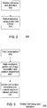
- FIG. 2 is a flow diagram of a method 200 for array defect detection and classification in accordance with an embodiment of the invention.
- the method 200 may include a golden cell set-up and definition procedure 300 and a procedure 900 for defect detection using a golden cell contour. Both of these procedures are described further below.
- various modes of inspection may be provided by the system, including array and non-array modes.
- a user may select an array mode of inspection.
- multiple detection techniques may be provided by the system.
- a user may select a contour-based detection technique.
- multiple types of reference cells may be used.
- a user may specify the reference type as a "golden cell" (i.e. a known defect-free cell).
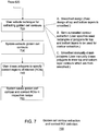
- FIG. 3 is a flow diagram of a golden cell set-up and definition procedure 300 in accordance with an embodiment of the invention.
- User input steps in this procedure may be implemented using a display screen and user interface (such as a mouse, touchscreen or trackball, for example).
- a pitch computation procedure 400 may be performed.
- An exemplary pitch computation procedure 400 is described below in relation to FIG. 4 .
- a procedure 600 for high-resolution golden cell image acquisition and position adjustment may be performed.
- An exemplary such procedure 600 is described below in relation to FIG. 6 .
- a golden cell contour extraction and context region of interest (ROI) definition procedure 700 may be performed.
- An exemplary such procedure 700 is described below in relation to FIG. 7 .
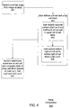
- FIG. 4 is a flow diagram of an exemplary pitch computation procedure 400 in accordance with an embodiment of the invention.
- this procedure 400 may be performed as part of the golden cell set-up and definition procedure 300 of FIG. 3 .
- User input steps in this procedure may be implemented using a display screen and user interface (such as a mouse, touchscreen or trackball, for example).
- the system may provide a large field of view (FoV) image of the array.
- the large FoV image shall be longer than one cell in each dimension.
- step 402 the user defines a unit cell and an array cell block within the large FoV image.
- the array cell block may be two-dimensional (with multiple cells arranged in a two-dimensional array) or one-dimensional (with multiple cells arranged in a one-dimensional array).
- step 402 may be implemented with steps 404 and 406.
- the user may select the top left (Cell Loc1) and bottom right (Cell Loc2) (i.e. opposite corners) of a unit cell at one corner of the array cell block.
- the defined unit cell may be the cell in the upper left corner of the array cell block.
- the user may select the bottom right (Cell Loc3) of the array cell block (i.e. the bottom right of the cell in the bottom right of the array cell block).
- the system may determine exact size of the unit cell and compute the pitch in each dimension of the array cell block. This determination may be based on the user inputs for Cell Loc1, Cell Loc2, and Cell Loc3.
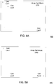
- FIG. 5A depicts example cell location selections for a two-dimensional cell array in accordance with an embodiment of the invention.
- Cell Loc1 and Cell Loc 2 define the opposite corners of a unit cell in the upper left of the array cell block.
- Cell Loc 3 defines the bottom right corner of the cell in the bottom right of the array cell block. From Cell Loc 1, Cell Loc 2, and Cell Loc 3, the horizontal and vertical pitches may be computed for the cells in the two-dimensional cell array.
- FIG. 5B depicts example cell location selections for a one-dimensional cell array in accordance with an embodiment of the invention.
- Cell Loc1 and Cell Loc 2 define the opposite corners of a unit cell at the left of the array cell block.
- Cell Loc 3 defines the bottom right corner of the cell at the right of the array cell block. From Cell Loc 1, Cell Loc 2, and Cell Loc 3, the horizontal pitch may be computed for the cells in the one-dimensional cell array.
- FIG. 6 is a flow diagram of a procedure 600 for high-resolution golden cell image acquisition and position adjustment in accordance with an embodiment of the invention.
- this procedure 600 may be performed after the pitch computation procedure 400 of FIG. 4 .
- User input steps in this procedure may be implemented using a display screen and user interface (such as a mouse, touchscreen or trackball, for example).
- the system may acquire a golden (i.e. previously-determined to be defect-free or "known good") cell image at high resolution.
- the golden cell image acquisition may include several steps in an exemplary implementation.
- the system may compute the number of field of views (FoVs) needed to acquire the golden cell image at a high resolution setting of the system. The computation of the number of FoVs may be based on the cell size, the positional uncertainty due to the stage, and the FoV (or pixel size).
- the multiple FoVs are acquired, each FoV covering part of the unit cell and overlapping adjacent FoVs.
- a lower-resolution i.e.
- the low-resolution image may be up-sampled per step 616.
- the up-sampling increases a number of pixels in the image so that the lower-resolution image may be compared pixel for pixel against the high-resolution images acquired in step 612.
- the high-resolution images may be aligned using the up-sampled lower resolution image as a guide to determine the alignment offsets.
- the high-resolution images may then be stitched based on the alignment offsets to generate the golden cell image at high resolution.
- the system may adjust a position of the golden cell image. As shown, the position adjustment may be performed using several steps in an exemplary implementation.
- a first step 622 the system may tile and stitch golden cells to generate a tiled-stitched golden multiple-cell image. This step may be performed by tiling copies of the high-resolution golden cell image and stitching together the tiled copies to create the tiled-stitched golden multiple-cell image.
- the high-resolution golden cell image is replicated and then stitched to create a high-resolution multiple-cell image.
- the system may overlay a rectangle over the tiled-stitched golden multiple-cell image.
- the rectangle may be sized according to the array pitch(es) previously determined.
- the user may then adjust the position of the rectangle to specify a corner (for example, the top-left corner) of a single stitched golden cell within the tiled-stitched golden multiple-cell image.
- the user may click on a button labeled "clip golden cell" to select a single golden cell based on the user-positioned rectangle. In other words, a smaller frame of pixels encompassing a single golden cell is selected at the desired position is obtained.
- FIG. 7 is a flow diagram of a procedure 700 for golden cell contour extraction and context ROI definition in accordance with an embodiment of the invention.
- This procedure 700 may be performed after the procedure 600 of FIG. 6 .
- User input steps in this procedure may be implemented using a display screen and user interface (such as a mouse, touchscreen or trackball, for example).
- the user may select a technique for extracting golden cell contours from the selected golden cell.
- multiple technique options may be provided, such as: A) a smoothed design technique; B) a semi-automated contour extraction technique; and C) a smoothed manually-drawn polygons technique.
- the smoothed design technique may involve smoothing pre-OPC design data of the top and bottom layers.
- the semi-automated contour extraction technique may be a watershed technique.
- the semi-automated contour extraction technique may involve a user specifying seed rectangles or polygons for top and bottom layers to be used for the contour extraction. In one implementation, polygons of the design may be used as the seeds for extracting the contours.
- the smoothed manually-drawn polygons technique may involve a user manually drawing polygons using an image editing tool to create top and bottom layer contours which may then be smoothed.
- the system may then extract golden cell contours using the selected technique.
- a contour may be defined and stored as a list of points or locations.
- the golden cell contours may then be overlaid on top of the golden cell image in the display to the user.
- the user may then draw polygons to specify context regions of interest (ROls).
- the context ROls are to be used for subsequent binning and nuisance filtering.
- the system may save the golden cell contour and context ROIs in an inspection recipe.
- the inspection recipe may be subsequently used to inspect an area of a substrate with the patterned array of cells.
- the golden cell contour and/or context ROIs may be used, for example, to create a mask image to provide user-specified segmentation for defect detection, nuisance filtering, and binning and/or classification.
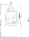
- FIG. 8 depicts example bottom-layer, top-layer and context ROI polygons within a stitched golden cell in accordance with an embodiment of the invention. Shown in FIG. 8 is an outline of a tiled-stitched golden multiple-cell image, and a selected stitched golden cell 820 therein. Also depicted are bottom layer (i.e. previous layer) polygons 830 and top layer (i.e. subsequent layer) polygons 840. In addition, example context ROI polygons 850 are depicted.
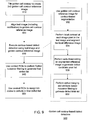
- FIG. 9 is a flow diagam of a procedure 900 for automated defect detection (i.e. automated inspection) using golden cell contours in accordance with an embodiment of the invention. This procedure 900 may be performed after the procedure 300 of FIG. 3 .
- the extracted golden cell contour may be tiled to create a corresponding 2x2 tiled golden cell contour reference image.
- some additional margin is added to create a reference image that is slightly larger than 2x2 cells so as to account for stage uncertainty.
- a test image may then be rectified and aligned to the golden cell contour reference image.
- the test image is an image of an area to be inspected for defects by comparison against the golden cell contour reference image.
- a contour-based defect detection procedure may be executed using the test image and the golden cell contour reference image. As depicted in FIG. 9 , this procedure may involve several steps.
- contour-based segmentation may be performed based on the contours of the golden cell contour reference image.
- the test image may be segmented or separated into regions based on the contours of the golden cell contour reference image.
- corners and/or contours at various distances from the edges of the golden cell contours may be segmented out to improve defect detection sensitivity.
- local contrast may be performed at each image pixel in the test image. The local difference image may then be segmented into image regions (or image segments) using the contour-based segmentation.
- a third step 936 auto-thresholding may be performed on the segmented difference image to generate a defect candidate pixel list.
- defect merging i.e. merging of candidate defect pixels
- attribute-based nuisance filtering may be performed to generate a defect blob list.
- the context ROls may be used to perform further nuisance filtering to generate a final defect list.
- the context ROls are used to assign bin codes to defects in the final defect list.
Landscapes
- Engineering & Computer Science (AREA)
- Physics & Mathematics (AREA)
- General Physics & Mathematics (AREA)
- Quality & Reliability (AREA)
- Computer Vision & Pattern Recognition (AREA)
- Theoretical Computer Science (AREA)
- Chemical & Material Sciences (AREA)
- Life Sciences & Earth Sciences (AREA)
- Health & Medical Sciences (AREA)
- Analytical Chemistry (AREA)
- Biochemistry (AREA)
- General Health & Medical Sciences (AREA)
- Immunology (AREA)
- Pathology (AREA)
- Analysing Materials By The Use Of Radiation (AREA)
- Testing Or Measuring Of Semiconductors Or The Like (AREA)
- Investigating Materials By The Use Of Optical Means Adapted For Particular Applications (AREA)
Applications Claiming Priority (3)
| Application Number | Priority Date | Filing Date | Title |
|---|---|---|---|
| US201361757807P | 2013-01-29 | 2013-01-29 | |
| US14/062,761 US9483819B2 (en) | 2013-01-29 | 2013-10-24 | Contour-based array inspection of patterned defects |
| PCT/US2014/013675 WO2014120828A1 (en) | 2013-01-29 | 2014-01-29 | Contour-based array inspection of patterned defects |
Publications (3)
| Publication Number | Publication Date |
|---|---|
| EP2951859A1 EP2951859A1 (en) | 2015-12-09 |
| EP2951859A4 EP2951859A4 (en) | 2016-09-28 |
| EP2951859B1 true EP2951859B1 (en) | 2019-09-18 |
Family
ID=51223005
Family Applications (1)
| Application Number | Title | Priority Date | Filing Date |
|---|---|---|---|
| EP14745726.1A Active EP2951859B1 (en) | 2013-01-29 | 2014-01-29 | Contour-based array inspection of patterned defects |
Country Status (6)
| Country | Link |
|---|---|
| US (1) | US9483819B2 (enExample) |
| EP (1) | EP2951859B1 (enExample) |
| JP (1) | JP6173487B2 (enExample) |
| KR (1) | KR102013481B1 (enExample) |
| TW (1) | TWI597494B (enExample) |
| WO (1) | WO2014120828A1 (enExample) |
Families Citing this family (18)
| Publication number | Priority date | Publication date | Assignee | Title |
|---|---|---|---|---|
| US9483819B2 (en) * | 2013-01-29 | 2016-11-01 | Kla-Tencor Corporation | Contour-based array inspection of patterned defects |
| TWI797699B (zh) | 2015-12-22 | 2023-04-01 | 以色列商應用材料以色列公司 | 半導體試樣的基於深度學習之檢查的方法及其系統 |
| WO2018099716A1 (en) * | 2016-12-01 | 2018-06-07 | Asml Netherlands B.V. | Method and system for pattern configuration |
| JP2019020292A (ja) * | 2017-07-19 | 2019-02-07 | 株式会社ニューフレアテクノロジー | パターン検査装置及びパターン検査方法 |
| KR102611427B1 (ko) * | 2017-10-02 | 2023-12-07 | 어플라이드 머티리얼즈 이스라엘 리미티드 | 패턴의 임계 치수 변동의 결정 |
| US10572991B2 (en) * | 2017-11-07 | 2020-02-25 | Kla-Tencor Corporation | System and method for aligning semiconductor device reference images and test images |
| EP3543791A1 (en) * | 2018-03-23 | 2019-09-25 | ASML Netherlands B.V. | Method of metrology and associated apparatuses |
| TWI854195B (zh) * | 2018-09-18 | 2024-09-01 | 荷蘭商Asml荷蘭公司 | 用於偵測快速充電裝置中時間相依缺陷的設備及方法 |
| CN109343303B (zh) * | 2018-10-24 | 2020-11-17 | 华中科技大学 | 一种基于内锥镜面扫描全景成像的微钻视觉检测方法及装置 |
| US11610296B2 (en) * | 2020-01-09 | 2023-03-21 | Kla Corporation | Projection and distance segmentation algorithm for wafer defect detection |
| KR102889846B1 (ko) | 2020-02-05 | 2025-11-26 | 삼성전자주식회사 | 광학적 근접 효과 보정의 검증 방법 |
| US11748872B2 (en) * | 2020-08-31 | 2023-09-05 | KLA Corp. | Setting up inspection of a specimen |
| CN115147329B (zh) * | 2021-03-29 | 2025-03-07 | 北京小米移动软件有限公司 | 一种柔性面板的修复方法、装置、设备及存储介质 |
| US12524867B2 (en) * | 2021-05-21 | 2026-01-13 | Kla Corporation | System and method for optical wafer characterization with image up-sampling |
| JP7624355B2 (ja) * | 2021-06-22 | 2025-01-30 | 株式会社日立ハイテク | 試料観察装置および方法 |
| KR20240035886A (ko) * | 2021-08-27 | 2024-03-18 | 주식회사 히타치하이테크 | 컴퓨터 시스템 및 해석 방법 |
| CN115511834A (zh) * | 2022-09-28 | 2022-12-23 | 广东利元亨智能装备股份有限公司 | 电芯对齐度检测方法、控制器、检测系统以及存储介质 |
| US12190500B2 (en) * | 2023-03-05 | 2025-01-07 | KLA Corp. | Detecting defects on specimens |
Citations (1)
| Publication number | Priority date | Publication date | Assignee | Title |
|---|---|---|---|---|
| US20130265408A1 (en) * | 2010-12-06 | 2013-10-10 | Kohei Yamaguchi | Charged particle beam apparatus |
Family Cites Families (31)
| Publication number | Priority date | Publication date | Assignee | Title |
|---|---|---|---|---|
| US6353222B1 (en) | 1998-09-03 | 2002-03-05 | Applied Materials, Inc. | Determining defect depth and contour information in wafer structures using multiple SEM images |
| US7796801B2 (en) | 1999-08-26 | 2010-09-14 | Nanogeometry Research Inc. | Pattern inspection apparatus and method |
| US6895106B2 (en) * | 2001-09-11 | 2005-05-17 | Eastman Kodak Company | Method for stitching partial radiation images to reconstruct a full image |
| JP3964267B2 (ja) | 2002-06-04 | 2007-08-22 | 大日本スクリーン製造株式会社 | 欠陥検出装置、欠陥検出方法、およびプログラム |
| US7076093B2 (en) * | 2002-09-16 | 2006-07-11 | Lee Shih-Jong J | Structure-guided image inspection |
| US20050157308A1 (en) | 2004-01-15 | 2005-07-21 | Andrei Brunfeld | Apparatus and method for measuring thickness variation of wax film |
| JP2005309140A (ja) | 2004-04-22 | 2005-11-04 | Toshiba Corp | フォトマスク製造方法、フォトマスク欠陥修正箇所判定方法、及びフォトマスク欠陥修正箇所判定装置 |
| JP4357355B2 (ja) | 2004-05-07 | 2009-11-04 | 株式会社日立ハイテクノロジーズ | パターン検査方法及びその装置 |
| KR100673014B1 (ko) | 2005-10-28 | 2007-01-24 | 삼성전자주식회사 | 포토 마스크의 제조 방법 |
| JP2007255959A (ja) | 2006-03-22 | 2007-10-04 | Lasertec Corp | 検査装置及び検査方法とその検査装置及び検査方法を用いたパターン基板の製造方法 |
| JP4943304B2 (ja) | 2006-12-05 | 2012-05-30 | 株式会社 Ngr | パターン検査装置および方法 |
| US7869643B2 (en) | 2007-01-31 | 2011-01-11 | Applied Materials South East Asia Pte. Ltd. | Advanced cell-to-cell inspection |
| KR100877105B1 (ko) | 2007-06-27 | 2009-01-07 | 주식회사 하이닉스반도체 | 반도체소자의 패턴 검증 방법 |
| JP4659004B2 (ja) | 2007-08-10 | 2011-03-30 | 株式会社日立ハイテクノロジーズ | 回路パターン検査方法、及び回路パターン検査システム |
| US8355562B2 (en) | 2007-08-23 | 2013-01-15 | Hitachi High-Technologies Corporation | Pattern shape evaluation method |
| KR20090042456A (ko) | 2007-10-26 | 2009-04-30 | 주식회사 하이닉스반도체 | 광 근접 보정을 위한 모델링 방법 |
| KR20090072670A (ko) | 2007-12-28 | 2009-07-02 | 주식회사 하이닉스반도체 | 노광마스크 형성방법 및 이를 이용한 반도체소자 형성방법 |
| JP5276854B2 (ja) | 2008-02-13 | 2013-08-28 | 株式会社日立ハイテクノロジーズ | パターン生成装置およびパターン形状評価装置 |
| JP6185693B2 (ja) | 2008-06-11 | 2017-08-23 | ケーエルエー−テンカー・コーポレーションKla−Tencor Corporation | ウェーハー上の設計欠陥および工程欠陥の検出、ウェーハー上の欠陥の精査、設計内の1つ以上の特徴を工程監視特徴として使用するための選択、またはそのいくつかの組み合わせのためのシステムおよび方法 |
| JP5572973B2 (ja) | 2009-03-16 | 2014-08-20 | 富士通セミコンダクター株式会社 | パターン検証方法、検証装置及びプログラム |
| KR101082102B1 (ko) | 2009-06-15 | 2011-11-10 | 주식회사 하이닉스반도체 | 웨이퍼패턴에 대한 광학근접보정 방법 |
| KR101342203B1 (ko) * | 2010-01-05 | 2013-12-16 | 가부시키가이샤 히다치 하이테크놀로지즈 | Sem을 이용한 결함 검사 방법 및 장치 |
| JP5422411B2 (ja) | 2010-01-22 | 2014-02-19 | 株式会社日立ハイテクノロジーズ | 荷電粒子線装置によって得られた画像データの輪郭線抽出方法、及び輪郭線抽出装置 |
| JP2011174858A (ja) | 2010-02-25 | 2011-09-08 | Toshiba Corp | 欠陥検出方法および半導体装置の製造方法 |
| US8477299B2 (en) | 2010-04-01 | 2013-07-02 | Taiwan Semiconductor Manufacturing Company, Ltd. | Method and apparatus for monitoring mask process impact on lithography performance |
| JP5722551B2 (ja) | 2010-05-13 | 2015-05-20 | 株式会社日立ハイテクノロジーズ | 欠陥検査方法及びその装置 |
| JPWO2011155122A1 (ja) * | 2010-06-07 | 2013-08-01 | 株式会社日立ハイテクノロジーズ | 回路パターン検査装置およびその検査方法 |
| JP5466142B2 (ja) * | 2010-12-15 | 2014-04-09 | アペリオ・テクノロジーズ・インコーポレイテッド | リニア・アレイを用いたマイクロスコープ・スライド・スキャナにおけるデータ管理システムおよび方法 |
| JP2012150065A (ja) | 2011-01-21 | 2012-08-09 | Hitachi High-Technologies Corp | 回路パターン検査装置およびその検査方法 |
| US8669523B2 (en) * | 2011-05-25 | 2014-03-11 | Kla-Tencor Corporation | Contour-based defect detection using an inspection apparatus |
| US9483819B2 (en) * | 2013-01-29 | 2016-11-01 | Kla-Tencor Corporation | Contour-based array inspection of patterned defects |
-
2013
- 2013-10-24 US US14/062,761 patent/US9483819B2/en active Active
-
2014
- 2014-01-29 WO PCT/US2014/013675 patent/WO2014120828A1/en not_active Ceased
- 2014-01-29 JP JP2015556115A patent/JP6173487B2/ja active Active
- 2014-01-29 KR KR1020157023400A patent/KR102013481B1/ko active Active
- 2014-01-29 TW TW103103669A patent/TWI597494B/zh active
- 2014-01-29 EP EP14745726.1A patent/EP2951859B1/en active Active
Patent Citations (1)
| Publication number | Priority date | Publication date | Assignee | Title |
|---|---|---|---|---|
| US20130265408A1 (en) * | 2010-12-06 | 2013-10-10 | Kohei Yamaguchi | Charged particle beam apparatus |
Also Published As
| Publication number | Publication date |
|---|---|
| KR102013481B1 (ko) | 2019-08-22 |
| WO2014120828A1 (en) | 2014-08-07 |
| US20140212024A1 (en) | 2014-07-31 |
| JP2016507058A (ja) | 2016-03-07 |
| TW201439526A (zh) | 2014-10-16 |
| EP2951859A4 (en) | 2016-09-28 |
| US9483819B2 (en) | 2016-11-01 |
| EP2951859A1 (en) | 2015-12-09 |
| KR20150112019A (ko) | 2015-10-06 |
| TWI597494B (zh) | 2017-09-01 |
| JP6173487B2 (ja) | 2017-08-02 |
Similar Documents
| Publication | Publication Date | Title |
|---|---|---|
| EP2951859B1 (en) | Contour-based array inspection of patterned defects | |
| US8669523B2 (en) | Contour-based defect detection using an inspection apparatus | |
| TWI517210B (zh) | Pattern evaluation method and pattern evaluation device | |
| JP5948138B2 (ja) | 欠陥解析支援装置、欠陥解析支援装置で実行されるプログラム、および欠陥解析システム | |
| KR102369848B1 (ko) | 관심 패턴 이미지 집단에 대한 이상치 검출 | |
| JP5202071B2 (ja) | 荷電粒子顕微鏡装置及びそれを用いた画像処理方法 | |
| US9342878B2 (en) | Charged particle beam apparatus | |
| US20120207397A1 (en) | Pattern Matching Method and Pattern Matching Apparatus | |
| US8502146B2 (en) | Methods and apparatus for classification of defects using surface height attributes | |
| KR101588367B1 (ko) | 하전 입자선 장치 | |
| US9082585B2 (en) | Defect observation method and device using SEM | |
| US8111902B2 (en) | Method and apparatus for inspecting defects of circuit patterns | |
| TW202136756A (zh) | 用於在檢查期間於樣本上界定彈性區域之系統及方法 | |
| US8884223B2 (en) | Methods and apparatus for measurement of relative critical dimensions | |
| JP2003218181A (ja) | 欠陥撮像装置 |
Legal Events
| Date | Code | Title | Description |
|---|---|---|---|
| PUAI | Public reference made under article 153(3) epc to a published international application that has entered the european phase |
Free format text: ORIGINAL CODE: 0009012 |
|
| 17P | Request for examination filed |
Effective date: 20150831 |
|
| AK | Designated contracting states |
Kind code of ref document: A1 Designated state(s): AL AT BE BG CH CY CZ DE DK EE ES FI FR GB GR HR HU IE IS IT LI LT LU LV MC MK MT NL NO PL PT RO RS SE SI SK SM TR |
|
| AX | Request for extension of the european patent |
Extension state: BA ME |
|
| DAX | Request for extension of the european patent (deleted) | ||
| REG | Reference to a national code |
Ref country code: DE Ref legal event code: R079 Ref document number: 602014053861 Country of ref document: DE Free format text: PREVIOUS MAIN CLASS: H01L0021660000 Ipc: G06T0007000000 |
|
| A4 | Supplementary search report drawn up and despatched |
Effective date: 20160831 |
|
| RIC1 | Information provided on ipc code assigned before grant |
Ipc: G06T 7/00 20060101AFI20160825BHEP Ipc: H01L 21/66 20060101ALI20160825BHEP |
|
| STAA | Information on the status of an ep patent application or granted ep patent |
Free format text: STATUS: EXAMINATION IS IN PROGRESS |
|
| 17Q | First examination report despatched |
Effective date: 20180214 |
|
| GRAP | Despatch of communication of intention to grant a patent |
Free format text: ORIGINAL CODE: EPIDOSNIGR1 |
|
| STAA | Information on the status of an ep patent application or granted ep patent |
Free format text: STATUS: GRANT OF PATENT IS INTENDED |
|
| INTG | Intention to grant announced |
Effective date: 20190412 |
|
| GRAS | Grant fee paid |
Free format text: ORIGINAL CODE: EPIDOSNIGR3 |
|
| GRAA | (expected) grant |
Free format text: ORIGINAL CODE: 0009210 |
|
| STAA | Information on the status of an ep patent application or granted ep patent |
Free format text: STATUS: THE PATENT HAS BEEN GRANTED |
|
| AK | Designated contracting states |
Kind code of ref document: B1 Designated state(s): AL AT BE BG CH CY CZ DE DK EE ES FI FR GB GR HR HU IE IS IT LI LT LU LV MC MK MT NL NO PL PT RO RS SE SI SK SM TR |
|
| REG | Reference to a national code |
Ref country code: GB Ref legal event code: FG4D |
|
| REG | Reference to a national code |
Ref country code: CH Ref legal event code: EP |
|
| REG | Reference to a national code |
Ref country code: DE Ref legal event code: R096 Ref document number: 602014053861 Country of ref document: DE |
|
| REG | Reference to a national code |
Ref country code: AT Ref legal event code: REF Ref document number: 1182202 Country of ref document: AT Kind code of ref document: T Effective date: 20191015 |
|
| REG | Reference to a national code |
Ref country code: IE Ref legal event code: FG4D |
|
| REG | Reference to a national code |
Ref country code: NL Ref legal event code: FP |
|
| PG25 | Lapsed in a contracting state [announced via postgrant information from national office to epo] |
Ref country code: FI Free format text: LAPSE BECAUSE OF FAILURE TO SUBMIT A TRANSLATION OF THE DESCRIPTION OR TO PAY THE FEE WITHIN THE PRESCRIBED TIME-LIMIT Effective date: 20190918 Ref country code: HR Free format text: LAPSE BECAUSE OF FAILURE TO SUBMIT A TRANSLATION OF THE DESCRIPTION OR TO PAY THE FEE WITHIN THE PRESCRIBED TIME-LIMIT Effective date: 20190918 Ref country code: SE Free format text: LAPSE BECAUSE OF FAILURE TO SUBMIT A TRANSLATION OF THE DESCRIPTION OR TO PAY THE FEE WITHIN THE PRESCRIBED TIME-LIMIT Effective date: 20190918 Ref country code: NO Free format text: LAPSE BECAUSE OF FAILURE TO SUBMIT A TRANSLATION OF THE DESCRIPTION OR TO PAY THE FEE WITHIN THE PRESCRIBED TIME-LIMIT Effective date: 20191218 Ref country code: LT Free format text: LAPSE BECAUSE OF FAILURE TO SUBMIT A TRANSLATION OF THE DESCRIPTION OR TO PAY THE FEE WITHIN THE PRESCRIBED TIME-LIMIT Effective date: 20190918 Ref country code: BG Free format text: LAPSE BECAUSE OF FAILURE TO SUBMIT A TRANSLATION OF THE DESCRIPTION OR TO PAY THE FEE WITHIN THE PRESCRIBED TIME-LIMIT Effective date: 20191218 |
|
| REG | Reference to a national code |
Ref country code: LT Ref legal event code: MG4D |
|
| PG25 | Lapsed in a contracting state [announced via postgrant information from national office to epo] |
Ref country code: GR Free format text: LAPSE BECAUSE OF FAILURE TO SUBMIT A TRANSLATION OF THE DESCRIPTION OR TO PAY THE FEE WITHIN THE PRESCRIBED TIME-LIMIT Effective date: 20191219 Ref country code: LV Free format text: LAPSE BECAUSE OF FAILURE TO SUBMIT A TRANSLATION OF THE DESCRIPTION OR TO PAY THE FEE WITHIN THE PRESCRIBED TIME-LIMIT Effective date: 20190918 Ref country code: AL Free format text: LAPSE BECAUSE OF FAILURE TO SUBMIT A TRANSLATION OF THE DESCRIPTION OR TO PAY THE FEE WITHIN THE PRESCRIBED TIME-LIMIT Effective date: 20190918 Ref country code: RS Free format text: LAPSE BECAUSE OF FAILURE TO SUBMIT A TRANSLATION OF THE DESCRIPTION OR TO PAY THE FEE WITHIN THE PRESCRIBED TIME-LIMIT Effective date: 20190918 |
|
| REG | Reference to a national code |
Ref country code: AT Ref legal event code: MK05 Ref document number: 1182202 Country of ref document: AT Kind code of ref document: T Effective date: 20190918 |
|
| PG25 | Lapsed in a contracting state [announced via postgrant information from national office to epo] |
Ref country code: EE Free format text: LAPSE BECAUSE OF FAILURE TO SUBMIT A TRANSLATION OF THE DESCRIPTION OR TO PAY THE FEE WITHIN THE PRESCRIBED TIME-LIMIT Effective date: 20190918 Ref country code: PL Free format text: LAPSE BECAUSE OF FAILURE TO SUBMIT A TRANSLATION OF THE DESCRIPTION OR TO PAY THE FEE WITHIN THE PRESCRIBED TIME-LIMIT Effective date: 20190918 Ref country code: RO Free format text: LAPSE BECAUSE OF FAILURE TO SUBMIT A TRANSLATION OF THE DESCRIPTION OR TO PAY THE FEE WITHIN THE PRESCRIBED TIME-LIMIT Effective date: 20190918 Ref country code: ES Free format text: LAPSE BECAUSE OF FAILURE TO SUBMIT A TRANSLATION OF THE DESCRIPTION OR TO PAY THE FEE WITHIN THE PRESCRIBED TIME-LIMIT Effective date: 20190918 Ref country code: AT Free format text: LAPSE BECAUSE OF FAILURE TO SUBMIT A TRANSLATION OF THE DESCRIPTION OR TO PAY THE FEE WITHIN THE PRESCRIBED TIME-LIMIT Effective date: 20190918 Ref country code: PT Free format text: LAPSE BECAUSE OF FAILURE TO SUBMIT A TRANSLATION OF THE DESCRIPTION OR TO PAY THE FEE WITHIN THE PRESCRIBED TIME-LIMIT Effective date: 20200120 |
|
| PG25 | Lapsed in a contracting state [announced via postgrant information from national office to epo] |
Ref country code: SK Free format text: LAPSE BECAUSE OF FAILURE TO SUBMIT A TRANSLATION OF THE DESCRIPTION OR TO PAY THE FEE WITHIN THE PRESCRIBED TIME-LIMIT Effective date: 20190918 Ref country code: SM Free format text: LAPSE BECAUSE OF FAILURE TO SUBMIT A TRANSLATION OF THE DESCRIPTION OR TO PAY THE FEE WITHIN THE PRESCRIBED TIME-LIMIT Effective date: 20190918 Ref country code: IS Free format text: LAPSE BECAUSE OF FAILURE TO SUBMIT A TRANSLATION OF THE DESCRIPTION OR TO PAY THE FEE WITHIN THE PRESCRIBED TIME-LIMIT Effective date: 20200224 |
|
| REG | Reference to a national code |
Ref country code: DE Ref legal event code: R097 Ref document number: 602014053861 Country of ref document: DE |
|
| PLBE | No opposition filed within time limit |
Free format text: ORIGINAL CODE: 0009261 |
|
| STAA | Information on the status of an ep patent application or granted ep patent |
Free format text: STATUS: NO OPPOSITION FILED WITHIN TIME LIMIT |
|
| PG2D | Information on lapse in contracting state deleted |
Ref country code: IS |
|
| PG25 | Lapsed in a contracting state [announced via postgrant information from national office to epo] |
Ref country code: DK Free format text: LAPSE BECAUSE OF FAILURE TO SUBMIT A TRANSLATION OF THE DESCRIPTION OR TO PAY THE FEE WITHIN THE PRESCRIBED TIME-LIMIT Effective date: 20190918 Ref country code: IS Free format text: LAPSE BECAUSE OF FAILURE TO SUBMIT A TRANSLATION OF THE DESCRIPTION OR TO PAY THE FEE WITHIN THE PRESCRIBED TIME-LIMIT Effective date: 20200119 |
|
| 26N | No opposition filed |
Effective date: 20200619 |
|
| PG25 | Lapsed in a contracting state [announced via postgrant information from national office to epo] |
Ref country code: MC Free format text: LAPSE BECAUSE OF FAILURE TO SUBMIT A TRANSLATION OF THE DESCRIPTION OR TO PAY THE FEE WITHIN THE PRESCRIBED TIME-LIMIT Effective date: 20190918 Ref country code: SI Free format text: LAPSE BECAUSE OF FAILURE TO SUBMIT A TRANSLATION OF THE DESCRIPTION OR TO PAY THE FEE WITHIN THE PRESCRIBED TIME-LIMIT Effective date: 20190918 |
|
| REG | Reference to a national code |
Ref country code: CH Ref legal event code: PL |
|
| PG25 | Lapsed in a contracting state [announced via postgrant information from national office to epo] |
Ref country code: LU Free format text: LAPSE BECAUSE OF NON-PAYMENT OF DUE FEES Effective date: 20200129 |
|
| PG25 | Lapsed in a contracting state [announced via postgrant information from national office to epo] |
Ref country code: LI Free format text: LAPSE BECAUSE OF NON-PAYMENT OF DUE FEES Effective date: 20200131 Ref country code: CH Free format text: LAPSE BECAUSE OF NON-PAYMENT OF DUE FEES Effective date: 20200131 |
|
| PG25 | Lapsed in a contracting state [announced via postgrant information from national office to epo] |
Ref country code: IE Free format text: LAPSE BECAUSE OF NON-PAYMENT OF DUE FEES Effective date: 20200129 |
|
| PG25 | Lapsed in a contracting state [announced via postgrant information from national office to epo] |
Ref country code: TR Free format text: LAPSE BECAUSE OF FAILURE TO SUBMIT A TRANSLATION OF THE DESCRIPTION OR TO PAY THE FEE WITHIN THE PRESCRIBED TIME-LIMIT Effective date: 20190918 Ref country code: MT Free format text: LAPSE BECAUSE OF FAILURE TO SUBMIT A TRANSLATION OF THE DESCRIPTION OR TO PAY THE FEE WITHIN THE PRESCRIBED TIME-LIMIT Effective date: 20190918 Ref country code: CY Free format text: LAPSE BECAUSE OF FAILURE TO SUBMIT A TRANSLATION OF THE DESCRIPTION OR TO PAY THE FEE WITHIN THE PRESCRIBED TIME-LIMIT Effective date: 20190918 |
|
| PG25 | Lapsed in a contracting state [announced via postgrant information from national office to epo] |
Ref country code: MK Free format text: LAPSE BECAUSE OF FAILURE TO SUBMIT A TRANSLATION OF THE DESCRIPTION OR TO PAY THE FEE WITHIN THE PRESCRIBED TIME-LIMIT Effective date: 20190918 |
|
| P01 | Opt-out of the competence of the unified patent court (upc) registered |
Effective date: 20230525 |
|
| PGFP | Annual fee paid to national office [announced via postgrant information from national office to epo] |
Ref country code: NL Payment date: 20260126 Year of fee payment: 13 |
|
| PGFP | Annual fee paid to national office [announced via postgrant information from national office to epo] |
Ref country code: GB Payment date: 20260127 Year of fee payment: 13 |
|
| PGFP | Annual fee paid to national office [announced via postgrant information from national office to epo] |
Ref country code: DE Payment date: 20260128 Year of fee payment: 13 |
|
| PGFP | Annual fee paid to national office [announced via postgrant information from national office to epo] |
Ref country code: BE Payment date: 20260127 Year of fee payment: 13 Ref country code: IT Payment date: 20260121 Year of fee payment: 13 |
|
| PGFP | Annual fee paid to national office [announced via postgrant information from national office to epo] |
Ref country code: FR Payment date: 20260126 Year of fee payment: 13 |
|
| PGFP | Annual fee paid to national office [announced via postgrant information from national office to epo] |
Ref country code: CZ Payment date: 20260108 Year of fee payment: 13 |