EP2950358A2 - Gehäuse für lichtemittierende vorrichtung - Google Patents
Gehäuse für lichtemittierende vorrichtung Download PDFInfo
- Publication number
- EP2950358A2 EP2950358A2 EP15169338.9A EP15169338A EP2950358A2 EP 2950358 A2 EP2950358 A2 EP 2950358A2 EP 15169338 A EP15169338 A EP 15169338A EP 2950358 A2 EP2950358 A2 EP 2950358A2
- Authority
- EP
- European Patent Office
- Prior art keywords
- lead frame
- light emitting
- emitting device
- width
- conductive adhesive
- Prior art date
- Legal status (The legal status is an assumption and is not a legal conclusion. Google has not performed a legal analysis and makes no representation as to the accuracy of the status listed.)
- Granted
Links
- 239000000853 adhesive Substances 0.000 claims abstract description 115
- 230000001070 adhesive effect Effects 0.000 claims abstract description 115
- 230000008878 coupling Effects 0.000 claims description 9
- 238000010168 coupling process Methods 0.000 claims description 9
- 238000005859 coupling reaction Methods 0.000 claims description 9
- 229910000679 solder Inorganic materials 0.000 abstract description 22
- 239000004020 conductor Substances 0.000 abstract description 8
- 239000010410 layer Substances 0.000 description 59
- 239000004065 semiconductor Substances 0.000 description 38
- 239000000463 material Substances 0.000 description 24
- 238000000034 method Methods 0.000 description 14
- 230000008569 process Effects 0.000 description 13
- XLOMVQKBTHCTTD-UHFFFAOYSA-N Zinc monoxide Chemical compound [Zn]=O XLOMVQKBTHCTTD-UHFFFAOYSA-N 0.000 description 11
- 150000001875 compounds Chemical class 0.000 description 8
- 239000000758 substrate Substances 0.000 description 8
- 229910002704 AlGaN Inorganic materials 0.000 description 7
- -1 GaNA1InN Inorganic materials 0.000 description 7
- 239000002019 doping agent Substances 0.000 description 7
- 238000000465 moulding Methods 0.000 description 7
- 229920006336 epoxy molding compound Polymers 0.000 description 6
- 239000010931 gold Substances 0.000 description 6
- 239000004973 liquid crystal related substance Substances 0.000 description 6
- 229920005989 resin Polymers 0.000 description 6
- 239000011347 resin Substances 0.000 description 6
- 229920001187 thermosetting polymer Polymers 0.000 description 6
- 230000005540 biological transmission Effects 0.000 description 5
- 238000002310 reflectometry Methods 0.000 description 5
- 239000011787 zinc oxide Substances 0.000 description 5
- 229910001218 Gallium arsenide Inorganic materials 0.000 description 4
- 239000004698 Polyethylene Substances 0.000 description 4
- BQCADISMDOOEFD-UHFFFAOYSA-N Silver Chemical compound [Ag] BQCADISMDOOEFD-UHFFFAOYSA-N 0.000 description 4
- 230000006866 deterioration Effects 0.000 description 4
- 239000010408 film Substances 0.000 description 4
- PXHVJJICTQNCMI-UHFFFAOYSA-N nickel Substances [Ni] PXHVJJICTQNCMI-UHFFFAOYSA-N 0.000 description 4
- 230000003287 optical effect Effects 0.000 description 4
- 238000002161 passivation Methods 0.000 description 4
- 229920000573 polyethylene Polymers 0.000 description 4
- 229910052710 silicon Inorganic materials 0.000 description 4
- 229910052709 silver Inorganic materials 0.000 description 4
- 239000004332 silver Substances 0.000 description 4
- 229910000980 Aluminium gallium arsenide Inorganic materials 0.000 description 3
- 229910005540 GaP Inorganic materials 0.000 description 3
- VYPSYNLAJGMNEJ-UHFFFAOYSA-N Silicium dioxide Chemical compound O=[Si]=O VYPSYNLAJGMNEJ-UHFFFAOYSA-N 0.000 description 3
- XUIMIQQOPSSXEZ-UHFFFAOYSA-N Silicon Chemical compound [Si] XUIMIQQOPSSXEZ-UHFFFAOYSA-N 0.000 description 3
- 229910052782 aluminium Inorganic materials 0.000 description 3
- XAGFODPZIPBFFR-UHFFFAOYSA-N aluminium Chemical compound [Al] XAGFODPZIPBFFR-UHFFFAOYSA-N 0.000 description 3
- HTXDPTMKBJXEOW-UHFFFAOYSA-N dioxoiridium Chemical compound O=[Ir]=O HTXDPTMKBJXEOW-UHFFFAOYSA-N 0.000 description 3
- 230000000694 effects Effects 0.000 description 3
- 230000004907 flux Effects 0.000 description 3
- 239000011521 glass Substances 0.000 description 3
- PCHJSUWPFVWCPO-UHFFFAOYSA-N gold Chemical compound [Au] PCHJSUWPFVWCPO-UHFFFAOYSA-N 0.000 description 3
- 229910052737 gold Inorganic materials 0.000 description 3
- 229910000457 iridium oxide Inorganic materials 0.000 description 3
- 239000007788 liquid Substances 0.000 description 3
- 239000000203 mixture Substances 0.000 description 3
- 238000012986 modification Methods 0.000 description 3
- 230000004048 modification Effects 0.000 description 3
- 150000004767 nitrides Chemical class 0.000 description 3
- 239000003973 paint Substances 0.000 description 3
- 239000004417 polycarbonate Substances 0.000 description 3
- 229920000515 polycarbonate Polymers 0.000 description 3
- 229910001925 ruthenium oxide Inorganic materials 0.000 description 3
- WOCIAKWEIIZHES-UHFFFAOYSA-N ruthenium(iv) oxide Chemical compound O=[Ru]=O WOCIAKWEIIZHES-UHFFFAOYSA-N 0.000 description 3
- 230000035939 shock Effects 0.000 description 3
- 239000010703 silicon Substances 0.000 description 3
- 239000002210 silicon-based material Substances 0.000 description 3
- 239000002356 single layer Substances 0.000 description 3
- 229920003002 synthetic resin Polymers 0.000 description 3
- 239000000057 synthetic resin Substances 0.000 description 3
- GYHNNYVSQQEPJS-UHFFFAOYSA-N Gallium Chemical compound [Ga] GYHNNYVSQQEPJS-UHFFFAOYSA-N 0.000 description 2
- 239000004743 Polypropylene Substances 0.000 description 2
- 230000004888 barrier function Effects 0.000 description 2
- 230000000903 blocking effect Effects 0.000 description 2
- 239000010949 copper Substances 0.000 description 2
- 230000006378 damage Effects 0.000 description 2
- JAONJTDQXUSBGG-UHFFFAOYSA-N dialuminum;dizinc;oxygen(2-) Chemical compound [O-2].[O-2].[O-2].[O-2].[O-2].[Al+3].[Al+3].[Zn+2].[Zn+2] JAONJTDQXUSBGG-UHFFFAOYSA-N 0.000 description 2
- 238000009826 distribution Methods 0.000 description 2
- 230000007613 environmental effect Effects 0.000 description 2
- 230000004927 fusion Effects 0.000 description 2
- 229910052733 gallium Inorganic materials 0.000 description 2
- 229910052738 indium Inorganic materials 0.000 description 2
- APFVFJFRJDLVQX-UHFFFAOYSA-N indium atom Chemical compound [In] APFVFJFRJDLVQX-UHFFFAOYSA-N 0.000 description 2
- 239000011810 insulating material Substances 0.000 description 2
- 238000009413 insulation Methods 0.000 description 2
- 239000012774 insulation material Substances 0.000 description 2
- 239000007769 metal material Substances 0.000 description 2
- 229910000480 nickel oxide Inorganic materials 0.000 description 2
- 229920003229 poly(methyl methacrylate) Polymers 0.000 description 2
- 229920000139 polyethylene terephthalate Polymers 0.000 description 2
- 239000005020 polyethylene terephthalate Substances 0.000 description 2
- 239000002861 polymer material Substances 0.000 description 2
- 239000004926 polymethyl methacrylate Substances 0.000 description 2
- 229920001155 polypropylene Polymers 0.000 description 2
- 239000002904 solvent Substances 0.000 description 2
- SKRWFPLZQAAQSU-UHFFFAOYSA-N stibanylidynetin;hydrate Chemical compound O.[Sn].[Sb] SKRWFPLZQAAQSU-UHFFFAOYSA-N 0.000 description 2
- 239000000126 substance Substances 0.000 description 2
- 230000003746 surface roughness Effects 0.000 description 2
- 239000010936 titanium Substances 0.000 description 2
- 239000011800 void material Substances 0.000 description 2
- 238000004383 yellowing Methods 0.000 description 2
- 229910018229 Al—Ga Inorganic materials 0.000 description 1
- RYGMFSIKBFXOCR-UHFFFAOYSA-N Copper Chemical compound [Cu] RYGMFSIKBFXOCR-UHFFFAOYSA-N 0.000 description 1
- 239000004593 Epoxy Substances 0.000 description 1
- 229910002601 GaN Inorganic materials 0.000 description 1
- 229910000530 Gallium indium arsenide Inorganic materials 0.000 description 1
- RTAQQCXQSZGOHL-UHFFFAOYSA-N Titanium Chemical compound [Ti] RTAQQCXQSZGOHL-UHFFFAOYSA-N 0.000 description 1
- DZLPZFLXRVRDAE-UHFFFAOYSA-N [O--].[O--].[O--].[O--].[Al+3].[Zn++].[In+3] Chemical compound [O--].[O--].[O--].[O--].[Al+3].[Zn++].[In+3] DZLPZFLXRVRDAE-UHFFFAOYSA-N 0.000 description 1
- 229910052788 barium Inorganic materials 0.000 description 1
- 230000015572 biosynthetic process Effects 0.000 description 1
- 238000000071 blow moulding Methods 0.000 description 1
- 229910052791 calcium Inorganic materials 0.000 description 1
- 229910052681 coesite Inorganic materials 0.000 description 1
- 239000003086 colorant Substances 0.000 description 1
- 238000004891 communication Methods 0.000 description 1
- 239000000470 constituent Substances 0.000 description 1
- 229910052802 copper Inorganic materials 0.000 description 1
- 229910052906 cristobalite Inorganic materials 0.000 description 1
- 230000007547 defect Effects 0.000 description 1
- 230000002950 deficient Effects 0.000 description 1
- 238000011161 development Methods 0.000 description 1
- 230000005684 electric field Effects 0.000 description 1
- 238000005530 etching Methods 0.000 description 1
- 238000000605 extraction Methods 0.000 description 1
- YZZNJYQZJKSEER-UHFFFAOYSA-N gallium tin Chemical compound [Ga].[Sn] YZZNJYQZJKSEER-UHFFFAOYSA-N 0.000 description 1
- QZQVBEXLDFYHSR-UHFFFAOYSA-N gallium(III) oxide Inorganic materials O=[Ga]O[Ga]=O QZQVBEXLDFYHSR-UHFFFAOYSA-N 0.000 description 1
- 229910052732 germanium Inorganic materials 0.000 description 1
- 230000005484 gravity Effects 0.000 description 1
- 238000010438 heat treatment Methods 0.000 description 1
- 230000006872 improvement Effects 0.000 description 1
- AMGQUBHHOARCQH-UHFFFAOYSA-N indium;oxotin Chemical compound [In].[Sn]=O AMGQUBHHOARCQH-UHFFFAOYSA-N 0.000 description 1
- HRHKULZDDYWVBE-UHFFFAOYSA-N indium;oxozinc;tin Chemical compound [In].[Sn].[Zn]=O HRHKULZDDYWVBE-UHFFFAOYSA-N 0.000 description 1
- 238000001746 injection moulding Methods 0.000 description 1
- 238000003780 insertion Methods 0.000 description 1
- 230000037431 insertion Effects 0.000 description 1
- 230000031700 light absorption Effects 0.000 description 1
- 229910052749 magnesium Inorganic materials 0.000 description 1
- 238000004519 manufacturing process Methods 0.000 description 1
- 239000011159 matrix material Substances 0.000 description 1
- 229910052751 metal Inorganic materials 0.000 description 1
- 239000002184 metal Substances 0.000 description 1
- 229910052759 nickel Inorganic materials 0.000 description 1
- 230000005693 optoelectronics Effects 0.000 description 1
- TWNQGVIAIRXVLR-UHFFFAOYSA-N oxo(oxoalumanyloxy)alumane Chemical compound O=[Al]O[Al]=O TWNQGVIAIRXVLR-UHFFFAOYSA-N 0.000 description 1
- GNRSAWUEBMWBQH-UHFFFAOYSA-N oxonickel Chemical compound [Ni]=O GNRSAWUEBMWBQH-UHFFFAOYSA-N 0.000 description 1
- 230000035515 penetration Effects 0.000 description 1
- 239000004033 plastic Substances 0.000 description 1
- 229920003023 plastic Polymers 0.000 description 1
- 239000000843 powder Substances 0.000 description 1
- 230000002265 prevention Effects 0.000 description 1
- 239000002096 quantum dot Substances 0.000 description 1
- 230000004044 response Effects 0.000 description 1
- 229910052711 selenium Inorganic materials 0.000 description 1
- 238000000926 separation method Methods 0.000 description 1
- HBMJWWWQQXIZIP-UHFFFAOYSA-N silicon carbide Chemical compound [Si+]#[C-] HBMJWWWQQXIZIP-UHFFFAOYSA-N 0.000 description 1
- 239000000377 silicon dioxide Substances 0.000 description 1
- 229910052814 silicon oxide Inorganic materials 0.000 description 1
- 239000007787 solid Substances 0.000 description 1
- 230000007480 spreading Effects 0.000 description 1
- 238000003892 spreading Methods 0.000 description 1
- 229910052682 stishovite Inorganic materials 0.000 description 1
- 229910052712 strontium Inorganic materials 0.000 description 1
- 229910052714 tellurium Inorganic materials 0.000 description 1
- 239000010409 thin film Substances 0.000 description 1
- 229910052718 tin Inorganic materials 0.000 description 1
- 229910001887 tin oxide Inorganic materials 0.000 description 1
- 229910052719 titanium Inorganic materials 0.000 description 1
- 238000012546 transfer Methods 0.000 description 1
- 229910052905 tridymite Inorganic materials 0.000 description 1
- 229910052725 zinc Inorganic materials 0.000 description 1
- 239000011701 zinc Substances 0.000 description 1
- YVTHLONGBIQYBO-UHFFFAOYSA-N zinc indium(3+) oxygen(2-) Chemical compound [O--].[Zn++].[In+3] YVTHLONGBIQYBO-UHFFFAOYSA-N 0.000 description 1
Images


Classifications
-
- H—ELECTRICITY
- H01—ELECTRIC ELEMENTS
- H01L—SEMICONDUCTOR DEVICES NOT COVERED BY CLASS H10
- H01L33/00—Semiconductor devices with at least one potential-jump barrier or surface barrier specially adapted for light emission; Processes or apparatus specially adapted for the manufacture or treatment thereof or of parts thereof; Details thereof
- H01L33/48—Semiconductor devices with at least one potential-jump barrier or surface barrier specially adapted for light emission; Processes or apparatus specially adapted for the manufacture or treatment thereof or of parts thereof; Details thereof characterised by the semiconductor body packages
- H01L33/62—Arrangements for conducting electric current to or from the semiconductor body, e.g. lead-frames, wire-bonds or solder balls
-
- H—ELECTRICITY
- H01—ELECTRIC ELEMENTS
- H01L—SEMICONDUCTOR DEVICES NOT COVERED BY CLASS H10
- H01L24/00—Arrangements for connecting or disconnecting semiconductor or solid-state bodies; Methods or apparatus related thereto
- H01L24/01—Means for bonding being attached to, or being formed on, the surface to be connected, e.g. chip-to-package, die-attach, "first-level" interconnects; Manufacturing methods related thereto
- H01L24/10—Bump connectors ; Manufacturing methods related thereto
- H01L24/12—Structure, shape, material or disposition of the bump connectors prior to the connecting process
- H01L24/14—Structure, shape, material or disposition of the bump connectors prior to the connecting process of a plurality of bump connectors
-
- H—ELECTRICITY
- H01—ELECTRIC ELEMENTS
- H01L—SEMICONDUCTOR DEVICES NOT COVERED BY CLASS H10
- H01L24/00—Arrangements for connecting or disconnecting semiconductor or solid-state bodies; Methods or apparatus related thereto
- H01L24/01—Means for bonding being attached to, or being formed on, the surface to be connected, e.g. chip-to-package, die-attach, "first-level" interconnects; Manufacturing methods related thereto
- H01L24/10—Bump connectors ; Manufacturing methods related thereto
- H01L24/15—Structure, shape, material or disposition of the bump connectors after the connecting process
- H01L24/16—Structure, shape, material or disposition of the bump connectors after the connecting process of an individual bump connector
-
- H—ELECTRICITY
- H01—ELECTRIC ELEMENTS
- H01L—SEMICONDUCTOR DEVICES NOT COVERED BY CLASS H10
- H01L24/00—Arrangements for connecting or disconnecting semiconductor or solid-state bodies; Methods or apparatus related thereto
- H01L24/01—Means for bonding being attached to, or being formed on, the surface to be connected, e.g. chip-to-package, die-attach, "first-level" interconnects; Manufacturing methods related thereto
- H01L24/10—Bump connectors ; Manufacturing methods related thereto
- H01L24/15—Structure, shape, material or disposition of the bump connectors after the connecting process
- H01L24/17—Structure, shape, material or disposition of the bump connectors after the connecting process of a plurality of bump connectors
-
- H—ELECTRICITY
- H01—ELECTRIC ELEMENTS
- H01L—SEMICONDUCTOR DEVICES NOT COVERED BY CLASS H10
- H01L33/00—Semiconductor devices with at least one potential-jump barrier or surface barrier specially adapted for light emission; Processes or apparatus specially adapted for the manufacture or treatment thereof or of parts thereof; Details thereof
- H01L33/36—Semiconductor devices with at least one potential-jump barrier or surface barrier specially adapted for light emission; Processes or apparatus specially adapted for the manufacture or treatment thereof or of parts thereof; Details thereof characterised by the electrodes
- H01L33/38—Semiconductor devices with at least one potential-jump barrier or surface barrier specially adapted for light emission; Processes or apparatus specially adapted for the manufacture or treatment thereof or of parts thereof; Details thereof characterised by the electrodes with a particular shape
-
- H—ELECTRICITY
- H01—ELECTRIC ELEMENTS
- H01L—SEMICONDUCTOR DEVICES NOT COVERED BY CLASS H10
- H01L2224/00—Indexing scheme for arrangements for connecting or disconnecting semiconductor or solid-state bodies and methods related thereto as covered by H01L24/00
- H01L2224/01—Means for bonding being attached to, or being formed on, the surface to be connected, e.g. chip-to-package, die-attach, "first-level" interconnects; Manufacturing methods related thereto
- H01L2224/02—Bonding areas; Manufacturing methods related thereto
- H01L2224/04—Structure, shape, material or disposition of the bonding areas prior to the connecting process
- H01L2224/06—Structure, shape, material or disposition of the bonding areas prior to the connecting process of a plurality of bonding areas
- H01L2224/061—Disposition
- H01L2224/06102—Disposition the bonding areas being at different heights
-
- H—ELECTRICITY
- H01—ELECTRIC ELEMENTS
- H01L—SEMICONDUCTOR DEVICES NOT COVERED BY CLASS H10
- H01L2224/00—Indexing scheme for arrangements for connecting or disconnecting semiconductor or solid-state bodies and methods related thereto as covered by H01L24/00
- H01L2224/01—Means for bonding being attached to, or being formed on, the surface to be connected, e.g. chip-to-package, die-attach, "first-level" interconnects; Manufacturing methods related thereto
- H01L2224/10—Bump connectors; Manufacturing methods related thereto
- H01L2224/12—Structure, shape, material or disposition of the bump connectors prior to the connecting process
- H01L2224/13—Structure, shape, material or disposition of the bump connectors prior to the connecting process of an individual bump connector
- H01L2224/13001—Core members of the bump connector
- H01L2224/1301—Shape
- H01L2224/13016—Shape in side view
- H01L2224/13017—Shape in side view being non uniform along the bump connector
-
- H—ELECTRICITY
- H01—ELECTRIC ELEMENTS
- H01L—SEMICONDUCTOR DEVICES NOT COVERED BY CLASS H10
- H01L2224/00—Indexing scheme for arrangements for connecting or disconnecting semiconductor or solid-state bodies and methods related thereto as covered by H01L24/00
- H01L2224/01—Means for bonding being attached to, or being formed on, the surface to be connected, e.g. chip-to-package, die-attach, "first-level" interconnects; Manufacturing methods related thereto
- H01L2224/10—Bump connectors; Manufacturing methods related thereto
- H01L2224/12—Structure, shape, material or disposition of the bump connectors prior to the connecting process
- H01L2224/13—Structure, shape, material or disposition of the bump connectors prior to the connecting process of an individual bump connector
- H01L2224/13001—Core members of the bump connector
- H01L2224/13099—Material
- H01L2224/131—Material with a principal constituent of the material being a metal or a metalloid, e.g. boron [B], silicon [Si], germanium [Ge], arsenic [As], antimony [Sb], tellurium [Te] and polonium [Po], and alloys thereof
- H01L2224/13138—Material with a principal constituent of the material being a metal or a metalloid, e.g. boron [B], silicon [Si], germanium [Ge], arsenic [As], antimony [Sb], tellurium [Te] and polonium [Po], and alloys thereof the principal constituent melting at a temperature of greater than or equal to 950°C and less than 1550°C
- H01L2224/13139—Silver [Ag] as principal constituent
-
- H—ELECTRICITY
- H01—ELECTRIC ELEMENTS
- H01L—SEMICONDUCTOR DEVICES NOT COVERED BY CLASS H10
- H01L2224/00—Indexing scheme for arrangements for connecting or disconnecting semiconductor or solid-state bodies and methods related thereto as covered by H01L24/00
- H01L2224/01—Means for bonding being attached to, or being formed on, the surface to be connected, e.g. chip-to-package, die-attach, "first-level" interconnects; Manufacturing methods related thereto
- H01L2224/10—Bump connectors; Manufacturing methods related thereto
- H01L2224/12—Structure, shape, material or disposition of the bump connectors prior to the connecting process
- H01L2224/13—Structure, shape, material or disposition of the bump connectors prior to the connecting process of an individual bump connector
- H01L2224/13001—Core members of the bump connector
- H01L2224/13099—Material
- H01L2224/131—Material with a principal constituent of the material being a metal or a metalloid, e.g. boron [B], silicon [Si], germanium [Ge], arsenic [As], antimony [Sb], tellurium [Te] and polonium [Po], and alloys thereof
- H01L2224/13138—Material with a principal constituent of the material being a metal or a metalloid, e.g. boron [B], silicon [Si], germanium [Ge], arsenic [As], antimony [Sb], tellurium [Te] and polonium [Po], and alloys thereof the principal constituent melting at a temperature of greater than or equal to 950°C and less than 1550°C
- H01L2224/13144—Gold [Au] as principal constituent
-
- H—ELECTRICITY
- H01—ELECTRIC ELEMENTS
- H01L—SEMICONDUCTOR DEVICES NOT COVERED BY CLASS H10
- H01L2224/00—Indexing scheme for arrangements for connecting or disconnecting semiconductor or solid-state bodies and methods related thereto as covered by H01L24/00
- H01L2224/01—Means for bonding being attached to, or being formed on, the surface to be connected, e.g. chip-to-package, die-attach, "first-level" interconnects; Manufacturing methods related thereto
- H01L2224/10—Bump connectors; Manufacturing methods related thereto
- H01L2224/12—Structure, shape, material or disposition of the bump connectors prior to the connecting process
- H01L2224/13—Structure, shape, material or disposition of the bump connectors prior to the connecting process of an individual bump connector
- H01L2224/13001—Core members of the bump connector
- H01L2224/13099—Material
- H01L2224/13198—Material with a principal constituent of the material being a combination of two or more materials in the form of a matrix with a filler, i.e. being a hybrid material, e.g. segmented structures, foams
- H01L2224/13199—Material of the matrix
- H01L2224/13294—Material of the matrix with a principal constituent of the material being a liquid not provided for in groups H01L2224/132 - H01L2224/13291
-
- H—ELECTRICITY
- H01—ELECTRIC ELEMENTS
- H01L—SEMICONDUCTOR DEVICES NOT COVERED BY CLASS H10
- H01L2224/00—Indexing scheme for arrangements for connecting or disconnecting semiconductor or solid-state bodies and methods related thereto as covered by H01L24/00
- H01L2224/01—Means for bonding being attached to, or being formed on, the surface to be connected, e.g. chip-to-package, die-attach, "first-level" interconnects; Manufacturing methods related thereto
- H01L2224/10—Bump connectors; Manufacturing methods related thereto
- H01L2224/12—Structure, shape, material or disposition of the bump connectors prior to the connecting process
- H01L2224/13—Structure, shape, material or disposition of the bump connectors prior to the connecting process of an individual bump connector
- H01L2224/13001—Core members of the bump connector
- H01L2224/13099—Material
- H01L2224/13198—Material with a principal constituent of the material being a combination of two or more materials in the form of a matrix with a filler, i.e. being a hybrid material, e.g. segmented structures, foams
- H01L2224/13298—Fillers
- H01L2224/13299—Base material
- H01L2224/133—Base material with a principal constituent of the material being a metal or a metalloid, e.g. boron [B], silicon [Si], germanium [Ge], arsenic [As], antimony [Sb], tellurium [Te] and polonium [Po], and alloys thereof
-
- H—ELECTRICITY
- H01—ELECTRIC ELEMENTS
- H01L—SEMICONDUCTOR DEVICES NOT COVERED BY CLASS H10
- H01L2224/00—Indexing scheme for arrangements for connecting or disconnecting semiconductor or solid-state bodies and methods related thereto as covered by H01L24/00
- H01L2224/01—Means for bonding being attached to, or being formed on, the surface to be connected, e.g. chip-to-package, die-attach, "first-level" interconnects; Manufacturing methods related thereto
- H01L2224/10—Bump connectors; Manufacturing methods related thereto
- H01L2224/12—Structure, shape, material or disposition of the bump connectors prior to the connecting process
- H01L2224/14—Structure, shape, material or disposition of the bump connectors prior to the connecting process of a plurality of bump connectors
- H01L2224/1401—Structure
- H01L2224/1403—Bump connectors having different sizes, e.g. different diameters, heights or widths
-
- H—ELECTRICITY
- H01—ELECTRIC ELEMENTS
- H01L—SEMICONDUCTOR DEVICES NOT COVERED BY CLASS H10
- H01L2224/00—Indexing scheme for arrangements for connecting or disconnecting semiconductor or solid-state bodies and methods related thereto as covered by H01L24/00
- H01L2224/01—Means for bonding being attached to, or being formed on, the surface to be connected, e.g. chip-to-package, die-attach, "first-level" interconnects; Manufacturing methods related thereto
- H01L2224/10—Bump connectors; Manufacturing methods related thereto
- H01L2224/15—Structure, shape, material or disposition of the bump connectors after the connecting process
- H01L2224/16—Structure, shape, material or disposition of the bump connectors after the connecting process of an individual bump connector
- H01L2224/1605—Shape
- H01L2224/16057—Shape in side view
- H01L2224/16058—Shape in side view being non uniform along the bump connector
-
- H—ELECTRICITY
- H01—ELECTRIC ELEMENTS
- H01L—SEMICONDUCTOR DEVICES NOT COVERED BY CLASS H10
- H01L2224/00—Indexing scheme for arrangements for connecting or disconnecting semiconductor or solid-state bodies and methods related thereto as covered by H01L24/00
- H01L2224/01—Means for bonding being attached to, or being formed on, the surface to be connected, e.g. chip-to-package, die-attach, "first-level" interconnects; Manufacturing methods related thereto
- H01L2224/10—Bump connectors; Manufacturing methods related thereto
- H01L2224/15—Structure, shape, material or disposition of the bump connectors after the connecting process
- H01L2224/16—Structure, shape, material or disposition of the bump connectors after the connecting process of an individual bump connector
- H01L2224/161—Disposition
- H01L2224/16151—Disposition the bump connector connecting between a semiconductor or solid-state body and an item not being a semiconductor or solid-state body, e.g. chip-to-substrate, chip-to-passive
- H01L2224/16221—Disposition the bump connector connecting between a semiconductor or solid-state body and an item not being a semiconductor or solid-state body, e.g. chip-to-substrate, chip-to-passive the body and the item being stacked
- H01L2224/16225—Disposition the bump connector connecting between a semiconductor or solid-state body and an item not being a semiconductor or solid-state body, e.g. chip-to-substrate, chip-to-passive the body and the item being stacked the item being non-metallic, e.g. insulating substrate with or without metallisation
- H01L2224/16227—Disposition the bump connector connecting between a semiconductor or solid-state body and an item not being a semiconductor or solid-state body, e.g. chip-to-substrate, chip-to-passive the body and the item being stacked the item being non-metallic, e.g. insulating substrate with or without metallisation the bump connector connecting to a bond pad of the item
-
- H—ELECTRICITY
- H01—ELECTRIC ELEMENTS
- H01L—SEMICONDUCTOR DEVICES NOT COVERED BY CLASS H10
- H01L2224/00—Indexing scheme for arrangements for connecting or disconnecting semiconductor or solid-state bodies and methods related thereto as covered by H01L24/00
- H01L2224/01—Means for bonding being attached to, or being formed on, the surface to be connected, e.g. chip-to-package, die-attach, "first-level" interconnects; Manufacturing methods related thereto
- H01L2224/10—Bump connectors; Manufacturing methods related thereto
- H01L2224/15—Structure, shape, material or disposition of the bump connectors after the connecting process
- H01L2224/16—Structure, shape, material or disposition of the bump connectors after the connecting process of an individual bump connector
- H01L2224/161—Disposition
- H01L2224/16151—Disposition the bump connector connecting between a semiconductor or solid-state body and an item not being a semiconductor or solid-state body, e.g. chip-to-substrate, chip-to-passive
- H01L2224/16221—Disposition the bump connector connecting between a semiconductor or solid-state body and an item not being a semiconductor or solid-state body, e.g. chip-to-substrate, chip-to-passive the body and the item being stacked
- H01L2224/16245—Disposition the bump connector connecting between a semiconductor or solid-state body and an item not being a semiconductor or solid-state body, e.g. chip-to-substrate, chip-to-passive the body and the item being stacked the item being metallic
-
- H—ELECTRICITY
- H01—ELECTRIC ELEMENTS
- H01L—SEMICONDUCTOR DEVICES NOT COVERED BY CLASS H10
- H01L2224/00—Indexing scheme for arrangements for connecting or disconnecting semiconductor or solid-state bodies and methods related thereto as covered by H01L24/00
- H01L2224/01—Means for bonding being attached to, or being formed on, the surface to be connected, e.g. chip-to-package, die-attach, "first-level" interconnects; Manufacturing methods related thereto
- H01L2224/10—Bump connectors; Manufacturing methods related thereto
- H01L2224/15—Structure, shape, material or disposition of the bump connectors after the connecting process
- H01L2224/17—Structure, shape, material or disposition of the bump connectors after the connecting process of a plurality of bump connectors
- H01L2224/1701—Structure
- H01L2224/1703—Bump connectors having different sizes, e.g. different diameters, heights or widths
-
- H—ELECTRICITY
- H01—ELECTRIC ELEMENTS
- H01L—SEMICONDUCTOR DEVICES NOT COVERED BY CLASS H10
- H01L2224/00—Indexing scheme for arrangements for connecting or disconnecting semiconductor or solid-state bodies and methods related thereto as covered by H01L24/00
- H01L2224/01—Means for bonding being attached to, or being formed on, the surface to be connected, e.g. chip-to-package, die-attach, "first-level" interconnects; Manufacturing methods related thereto
- H01L2224/10—Bump connectors; Manufacturing methods related thereto
- H01L2224/15—Structure, shape, material or disposition of the bump connectors after the connecting process
- H01L2224/17—Structure, shape, material or disposition of the bump connectors after the connecting process of a plurality of bump connectors
- H01L2224/1705—Shape
- H01L2224/17051—Bump connectors having different shapes
-
- H—ELECTRICITY
- H01—ELECTRIC ELEMENTS
- H01L—SEMICONDUCTOR DEVICES NOT COVERED BY CLASS H10
- H01L2224/00—Indexing scheme for arrangements for connecting or disconnecting semiconductor or solid-state bodies and methods related thereto as covered by H01L24/00
- H01L2224/80—Methods for connecting semiconductor or other solid state bodies using means for bonding being attached to, or being formed on, the surface to be connected
- H01L2224/81—Methods for connecting semiconductor or other solid state bodies using means for bonding being attached to, or being formed on, the surface to be connected using a bump connector
- H01L2224/8119—Arrangement of the bump connectors prior to mounting
- H01L2224/81193—Arrangement of the bump connectors prior to mounting wherein the bump connectors are disposed on both the semiconductor or solid-state body and another item or body to be connected to the semiconductor or solid-state body
-
- H—ELECTRICITY
- H01—ELECTRIC ELEMENTS
- H01L—SEMICONDUCTOR DEVICES NOT COVERED BY CLASS H10
- H01L2224/00—Indexing scheme for arrangements for connecting or disconnecting semiconductor or solid-state bodies and methods related thereto as covered by H01L24/00
- H01L2224/80—Methods for connecting semiconductor or other solid state bodies using means for bonding being attached to, or being formed on, the surface to be connected
- H01L2224/81—Methods for connecting semiconductor or other solid state bodies using means for bonding being attached to, or being formed on, the surface to be connected using a bump connector
- H01L2224/8138—Bonding interfaces outside the semiconductor or solid-state body
- H01L2224/81399—Material
- H01L2224/814—Material with a principal constituent of the material being a metal or a metalloid, e.g. boron [B], silicon [Si], germanium [Ge], arsenic [As], antimony [Sb], tellurium [Te] and polonium [Po], and alloys thereof
- H01L2224/81438—Material with a principal constituent of the material being a metal or a metalloid, e.g. boron [B], silicon [Si], germanium [Ge], arsenic [As], antimony [Sb], tellurium [Te] and polonium [Po], and alloys thereof the principal constituent melting at a temperature of greater than or equal to 950°C and less than 1550°C
- H01L2224/81439—Silver [Ag] as principal constituent
-
- H—ELECTRICITY
- H01—ELECTRIC ELEMENTS
- H01L—SEMICONDUCTOR DEVICES NOT COVERED BY CLASS H10
- H01L2224/00—Indexing scheme for arrangements for connecting or disconnecting semiconductor or solid-state bodies and methods related thereto as covered by H01L24/00
- H01L2224/80—Methods for connecting semiconductor or other solid state bodies using means for bonding being attached to, or being formed on, the surface to be connected
- H01L2224/81—Methods for connecting semiconductor or other solid state bodies using means for bonding being attached to, or being formed on, the surface to be connected using a bump connector
- H01L2224/818—Bonding techniques
- H01L2224/81801—Soldering or alloying
- H01L2224/81815—Reflow soldering
-
- H—ELECTRICITY
- H01—ELECTRIC ELEMENTS
- H01L—SEMICONDUCTOR DEVICES NOT COVERED BY CLASS H10
- H01L24/00—Arrangements for connecting or disconnecting semiconductor or solid-state bodies; Methods or apparatus related thereto
- H01L24/01—Means for bonding being attached to, or being formed on, the surface to be connected, e.g. chip-to-package, die-attach, "first-level" interconnects; Manufacturing methods related thereto
- H01L24/10—Bump connectors ; Manufacturing methods related thereto
- H01L24/12—Structure, shape, material or disposition of the bump connectors prior to the connecting process
- H01L24/13—Structure, shape, material or disposition of the bump connectors prior to the connecting process of an individual bump connector
-
- H—ELECTRICITY
- H01—ELECTRIC ELEMENTS
- H01L—SEMICONDUCTOR DEVICES NOT COVERED BY CLASS H10
- H01L24/00—Arrangements for connecting or disconnecting semiconductor or solid-state bodies; Methods or apparatus related thereto
- H01L24/80—Methods for connecting semiconductor or other solid state bodies using means for bonding being attached to, or being formed on, the surface to be connected
- H01L24/81—Methods for connecting semiconductor or other solid state bodies using means for bonding being attached to, or being formed on, the surface to be connected using a bump connector
-
- H—ELECTRICITY
- H01—ELECTRIC ELEMENTS
- H01L—SEMICONDUCTOR DEVICES NOT COVERED BY CLASS H10
- H01L2924/00—Indexing scheme for arrangements or methods for connecting or disconnecting semiconductor or solid-state bodies as covered by H01L24/00
- H01L2924/10—Details of semiconductor or other solid state devices to be connected
- H01L2924/11—Device type
- H01L2924/12—Passive devices, e.g. 2 terminal devices
- H01L2924/1204—Optical Diode
- H01L2924/12041—LED
-
- H—ELECTRICITY
- H01—ELECTRIC ELEMENTS
- H01L—SEMICONDUCTOR DEVICES NOT COVERED BY CLASS H10
- H01L2933/00—Details relating to devices covered by the group H01L33/00 but not provided for in its subgroups
- H01L2933/0008—Processes
- H01L2933/0033—Processes relating to semiconductor body packages
- H01L2933/0066—Processes relating to semiconductor body packages relating to arrangements for conducting electric current to or from the semiconductor body
-
- H—ELECTRICITY
- H01—ELECTRIC ELEMENTS
- H01L—SEMICONDUCTOR DEVICES NOT COVERED BY CLASS H10
- H01L33/00—Semiconductor devices with at least one potential-jump barrier or surface barrier specially adapted for light emission; Processes or apparatus specially adapted for the manufacture or treatment thereof or of parts thereof; Details thereof
- H01L33/48—Semiconductor devices with at least one potential-jump barrier or surface barrier specially adapted for light emission; Processes or apparatus specially adapted for the manufacture or treatment thereof or of parts thereof; Details thereof characterised by the semiconductor body packages
- H01L33/483—Containers
- H01L33/486—Containers adapted for surface mounting
-
- H—ELECTRICITY
- H01—ELECTRIC ELEMENTS
- H01L—SEMICONDUCTOR DEVICES NOT COVERED BY CLASS H10
- H01L33/00—Semiconductor devices with at least one potential-jump barrier or surface barrier specially adapted for light emission; Processes or apparatus specially adapted for the manufacture or treatment thereof or of parts thereof; Details thereof
- H01L33/48—Semiconductor devices with at least one potential-jump barrier or surface barrier specially adapted for light emission; Processes or apparatus specially adapted for the manufacture or treatment thereof or of parts thereof; Details thereof characterised by the semiconductor body packages
- H01L33/58—Optical field-shaping elements
- H01L33/60—Reflective elements
-
- H—ELECTRICITY
- H01—ELECTRIC ELEMENTS
- H01L—SEMICONDUCTOR DEVICES NOT COVERED BY CLASS H10
- H01L33/00—Semiconductor devices with at least one potential-jump barrier or surface barrier specially adapted for light emission; Processes or apparatus specially adapted for the manufacture or treatment thereof or of parts thereof; Details thereof
- H01L33/48—Semiconductor devices with at least one potential-jump barrier or surface barrier specially adapted for light emission; Processes or apparatus specially adapted for the manufacture or treatment thereof or of parts thereof; Details thereof characterised by the semiconductor body packages
- H01L33/64—Heat extraction or cooling elements
- H01L33/647—Heat extraction or cooling elements the elements conducting electric current to or from the semiconductor body
Definitions
- Embodiments relate to a light emitting device package and, more particularly, improvement of reliability upon bonding of a light emitting device inside a package.
- Group III-V compound semiconductors such as, for example, GaN and AlGaN are widely used for optoelectronics and electronics because of many advantages such as, for example, easily controllable wide band gap energy.
- light emitting devices such as light emitting diodes or laser diodes, which use group III-V or II-VI compound semiconductors, are capable of emitting visible and ultraviolet light of various colors such as red, green, and blue owing to development of device materials and thin film growth techniques.
- These light emitting devices are also capable of emitting white light with high luminous efficacy through use of a fluorescent substance or color combination and have several advantages of low power consumption, semi-permanent lifespan, fast response speed, safety, and environmental friendliness as compared to conventional light sources such as, for example, fluorescent lamps and incandescent lamps.
- CCFLs Cold Cathode Fluorescence Lamps
- LCD Liquid Crystal Display
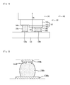
- FIG. 1 is a view illustrating a conventional light emitting device package
- FIG. 2 is a view illustrating the shape of a solder in detail.
- the conventional light emitting device package 100 includes a first lead frame 120a and a second lead frame 120b disposed on a sub-mount 110, and a light emitting device 140 is electrically coupled to the first lead frame 120a and the second lead frame 120b via solders 150a and 150b.
- the light emitting device 140 includes a substrate 141 and an underlying light emitting structure 142 including a first conductive semiconductor layer 142a, an active layer 142b, and a second conductive semiconductor layer 142c.
- the light emitting device 140 further includes a first electrode 144a disposed beneath one side of a lower surface of the first conductive semiconductor layer 142a and a second electrode 144b disposed beneath a lower surface of the second conductive semiconductor layer 142c, the first electrode 144a and the second electrode 144b being electrically connected to the first lead frame 120a and the second lead frame 120b respectively.
- the solders 150a and 150b are used for electrical connection between the light emitting device 140 and the first and second lead frames 120a and 120b. There may occur stress due to a difference between thermal expansion coefficients of different kinds of materials and, consequently, this stress may have a negative effect on the quality of the light emitting structure 142.
- a height h 01 of the light emitting device 140 is within a range of about 100 ⁇ m to 200 ⁇ m and a height h 02 of the solders 150a and 150b is within about 30 ⁇ m, there is sufficient probability that the stress is transferred to the light emitting device 140 through the solders 150a and 150b.
- the electrodes 144a and 144b of the light emitting device 140 are attached to the solders 150a and 150b.
- voids may be generated in an upper region of the solder 150b bonded to the second electrode 144b of the light emitting device 140.
- the voids as described above may be generated while an interface between the solder 150b and the second electrode 144b is cooled in a heat treatment process for the solder 150b. Such void generation may result in defective electrical connection between the second lead frame 120b and the second electrode 144b of the light emitting device 140 or may prevent uniform light distribution throughout the light emitting device package 100.
- the solder disposed between the electrode of the light emitting device and the lead frame may cause the light emitting device to deviate from a fixed position thereof during implementation of a reflow process.
- the solder when the solder is applied to a reflective layer disposed on the sub-mount to reflect light emitted from the light emitting device, light loss of the light emitting device package may occur.
- Embodiments provide a light emitting device package which is capable of improving reliability of electrical connection between a lead frame and a light emitting device and achieving uniform light distribution.
- a light emitting device package includes a package body, a first lead frame and a second lead frame disposed on the package body, and a light emitting device electrically connected to the first lead frame and the second lead frame via respective conductive adhesives, wherein at least one of the conductive adhesives has the smallest width at a central region thereof.
- Each of the conductive adhesives may be divided into a first portion and a second portion, and the central region is disposed between the first portion and the second portion.
- An end of the first portion of the conductive adhesive may contact with one of the first lead frame and the second lead frame and an end of the second portion of the conductive adhesive may contact with a first electrode or a second electrode of the light emitting device.
- the first portion may have a higher height than a height of the second portion.
- the end of the first portion of the conductive adhesive contacting with one of the first lead frame and the second lead frame may have a greater width than a width of the end of the second portion contacting with the first electrode or the second electrode of the light emitting device.
- the end of the first portion of the conductive adhesive contacting with one of the first lead frame and the second lead frame may have a smaller width than a width of a central region of the first portion of the conductive adhesive.
- the end of the first portion of the conductive adhesive contacting with one of the first lead frame and the second lead frame may have a greater width than a width of the central region of the conductive adhesive.
- the end of the second portion of the conductive adhesive contacting with one of the first electrode and the second electrode may have a smaller width than a width of a central region of the second portion of the conductive adhesive.
- the end of the second portion of the conductive adhesive contacting with one of the first electrode and the second electrode may have a greater width than a width of the central region of the conductive adhesive.
- the central region may be a coupling interface of the first portion and the second portion.
- the central region may be a void free region.
- a light emitting device package in another embodiment, includes a package body including a cavity and at least one recess formed in the bottom of the cavity, a light emitting device disposed on the recess, a first lead frame and a second lead frame spaced apart from each other in the horizontal direction different from the thickness direction of the package body in the recess, and a conductive adhesive disposed between the light emitting device and the first lead frame and the second lead frame, wherein the cavity includes a first bottom surface provided with the recess and a second bottom surface adjacent to the first bottom surface, and wherein the conductive adhesive is disposed on the first bottom surface.
- the recess may have a first width in the horizontal direction and the first width may be 0.9 times or more and 1.1 times or less of a second width of the light emitting device in the horizontal direction.
- the first lead frame and the second lead frame may penetrate the package body in the thickness direction and be exposed from the first bottom surface.
- the first lead frame and the second lead frame may be horizontally spaced apart from a boundary between the first bottom surface and the second bottom surface to thereby be exposed.
- the exposed first and second lead frames may contact with a boundary between the first bottom surface and the second bottom surface.
- the first bottom surface may have a first region disposed between the first lead frame and the second lead frame and a second region for exposure of the first and second lead frames, and the first region may protrude than the second region.
- the recess may have a smaller width than a width of the light emitting device.
- the recess may have a greater width than a width of the light emitting device.
- a light emitting device package includes a package body including a cavity and at least one recess formed in the bottom of the cavity, a light emitting device disposed on the recess, a first lead frame and a second lead frame spaced apart from each other in the horizontal direction different from the thickness direction of the package body in the recess, and conductive adhesives disposed between the light emitting device and the first lead frame and the second lead frame, wherein each of the conductive adhesives has a central region and is divided into a first portion and a second portion with the central region disposed therebetween, and wherein at least one of the conductive adhesives has the smallest width at the central region thereof.
- conductive adhesives are applied respectively to the light emitting device and the lead frame and, subsequently, the light emitting device and the lead frame are coupled to each other, which serves to prevent stress caused by a difference between thermal expansion coefficients from being transferred to a light emitting structure and to remove voids at an interface between the light emitting device and the lead frame.
- FIG. 3 is a view illustrating one embodiment of a light emitting device package.
- the light emitting device package as exemplarily illustrated in FIG. 3 designated by reference numeral 200, includes a package body 210 having a cavity, a first lead frame 220a and a second lead frame 220b disposed in the package body 210, a light emitting device 240 disposed in the package body 210 and electrically connected to the first lead frame 220a and the second lead frame 220b via conductive adhesives 310 and 320, and a molding part 260 received in the cavity to surround the light emitting device 240.
- the package body 210 may be formed of a silicon material, or may be formed of a synthetic resin material or a metal material. When the package body 210 is formed of a conductive material such as, for example, a metal material, although not illustrated, an insulation layer may be coated over the surface of the package body 210 to prevent electrical short-circuit between the first and second lead frames 220a and 220b.
- the cavity may be defined in the package body 210 and include a bottom surface, on which the light emitting device 240 is disposed, and a sidewall having a predetermined gradient relative to the bottom surface.
- the first lead frame 220a and the second lead frame 220b are disposed in the package body 210 so as to be electrically separated from each other and portions of the first lead frame 220a and the second lead frame 220b are exposed from the bottom surface of the cavity.
- the first lead frame 220a and the second lead frame 220b serve to supply current to the light emitting device 240.
- the first lead frame 220a and the second lead frame 220b are capable of increasing luminous efficacy by reflecting light emitted from the light emitting device 240 and outwardly radiating heat generated in the light emitting device 240.
- surfaces of the first and second lead frames 220a and 220b may be coated with, for example, silver (Ag) having excellent reflectivity, which may improve light extraction efficiency of the light emitting device package 200.
- the light emitting device 240 is a flip chip type light emitting device and includes a light emitting structure 242 disposed on a substrate 241, the light emitting structure 242 including a first conductive semiconductor layer 242a, an active layer 242b, and a second conductive semiconductor layer 242c.
- the substrate 241 may be formed of a material suitable for semiconductor material growth, or a carrier wafer.
- the substrate 241 may be formed of a highly thermally conductive material and include a conductive substrate or an insulation substrate.
- the substrate 241 may utilize at least one of sapphire (Al 2 O 3 ), SiO 2 , SiC, Si, GaAs, GaN, ZnO, GaP, InP, Ge, and Ga 2 O 3 .
- the first conductive semiconductor layer 242a may be formed of a compound semiconductor such as, for example, a group III-V or II-VI compound semiconductor and may be doped with a first conductive dopant.
- the first conductive semiconductor layer 242a may be formed of a semiconductor material having a composition of Al x In y Ga (1-x-y) N (0 ⁇ x ⁇ 1, 0 ⁇ y ⁇ 1, 0 ⁇ x+y ⁇ 1), i.e. any one or more materials selected from among AlGaN, GaN, InAlGaN, AlGaAs, GaP, GaAs, GaAsP, and AlGaInP.
- the first conductive dopant may include an n-type dopant such as Si, Ge, Sn, Se, and Te.
- the first conductive semiconductor layer 242a may have a single layer or multi-layer form, without being limited thereto.
- the active layer 242b is disposed between the first conductive semiconductor layer 242a and the second conductive semiconductor layer 242c and may include any one of a single-well structure, a multi-well structure, a single-quantum well structure, a multi-quantum well structure, a quantum dot structure and a quantum wire structure.
- the active layer 242b is formed of a group III-V compound semiconductor and includes a well layer and a barrier layer having a pair structure of any one or more of AlGaN/AlGaN, InGaN/GaN, InGaN/InGaN, AlGaN/GaN, InAlGaN/GaN, GaAs(InGaAs)/AlGaAs, and GaP(InGaP)/AlGaP, but is not limited thereto.
- the well layer may be formed of a material having a smaller energy band gap than an energy band gap of the barrier layer.
- the second conductive semiconductor layer 242c may be formed of a compound semiconductor.
- the second conductive semiconductor layer 242c may be formed of a compound semiconductor such as a group III-V or II-VI compound semiconductor and may be doped with a second conductive dopant.
- the second conductive semiconductor layer 242c may be formed of, for example, a semiconductor material having a composition of In x Al y Ga 1-x-y N (0 ⁇ x ⁇ 1, 0 ⁇ y ⁇ 1, 0 ⁇ x+y ⁇ 1), i.e. any one or more material selected from among AlGaN, GaNA1InN, AlGaAs, GaP, GaAs, GaAsP, and AlGaInP.
- the second conductive dopant may be a p-type dopant such as Mg, Zn, Ca, Sr, and Ba.
- the second conductive semiconductor layer 242c may have a single layer or multi-layer form, without being limited thereto.
- an electron blocking layer may be disposed between the active layer 242b and the second conductive semiconductor layer 242c.
- the electron blocking layer may have a superlattice structure.
- the superlattice structure may include an AlGaN layer doped with a second conductive dopant, or may include a plurality of GaN layers having different aluminum composition ratios that is alternately disposed.
- a light transmission conductive layer 245 is disposed on the second conductive semiconductor layer 242c.
- the light transmission conductive layer 245 may comprise at least one of Indium Tin Oxide (ITO), Indium Zinc Oxide (IZO), Indium Zinc Tin Oxide (IZTO), Indium Aluminum Zinc Oxide (IAZO), Indium Gallium Zinc Oxide (IGZO), Indium Gallium Tin Oxide (IGTO), Aluminum Zinc Oxide (AZO), Antimony Tin Oxide (ATO), Gallium Zinc Oxide (GZO), IZO nitride (IZON), Al-Ga ZnO (AGZO), In-Ga ZnO (IGZO), Zinc Oxide (ZnO), Iridium Oxide (IrOx), Ruthenium Oxide (RuOx), Nickel Oxide (NiO), RuOx/ITO, and Ni/IrOx/Au(Gold).
- ITO Indium Tin Oxide
- IZO Indium Zinc Oxide
- IZTO Indium
- first electrode 244a may be disposed on the first conductive semiconductor layer 242a.
- a portion of the surface of the first conductive semiconductor layer 242a may be exposed by etching portions of the light transmission conductive layer 245, the second conductive semiconductor layer 242c, the active layer 242b and the first conductive semiconductor layer 242a.
- the first electrode 244a may be disposed on the exposed surface portion.
- a passivation layer 248 may be formed around the light emitting structure 242.
- the passivation layer 248 may be formed of an insulation material.
- the insulation material may be a non-conductive oxide or nitride.
- the passivation layer 248 may be formed of a silicon oxide layer, an oxide nitride layer, or an oxide aluminum layer.
- the passivation layer 248 is not formed in areas where the first electrode 244a and the second electrode 244b are disposed.
- the first electrode 244a and the second electrode 244b of the light emitting device 240 may electrically contact with the first lead frame 220a and the second lead fame 220b respectively via the conductive adhesives 310 and 320.
- the conductive adhesives 310 and 320 may be formed of a conductive material such as, for example, silver (Ag), gold (Au) or a solder.
- the cavity may be filled with the molding part 260 surrounding the light emitting device 240.
- the molding part 260 may comprise a silicon or epoxy based substance and may contain phosphors 265.
- the phosphors 265 may be excited by light having a first wavelength emitted from the active layer 242b, thereby emitting light having a second wavelength that is longer than the first wavelength.
- the molding part 260 as described above may be formed of the same material as the package body 210 and, thus, assure inter-interface bonding without generation of cracks.
- the conductive adhesives 310 and 320 may be formed of a solder or any of other conductive materials and may have the smallest width at a central region thereof as illustrated.
- the width may mean a diameter when the conductive adhesives 310 and 320 have a circular horizontal cross section and may mean a length when the conductive adhesives 310 and 320 have a square horizontal cross section.
- a height h0 3 of the light emitting device 240 may be within a range of about 100 ⁇ m to 200 ⁇ m, and a height h 04 of the conductive adhesives 310 and 320 may be 30% to 50% of the height h 03 of the light emitting device 240, i.e. within a range of about 30 ⁇ m to 100 ⁇ m.
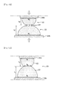
- FIGs. 4A and 4B are views illustrating embodiments of the conductive adhesive of FIG. 3 . Although one conductive adhesive 320, the second lead frame 220b and the second electrode 244b are illustrated, the following description may be applied to the other conductive adhesive 310, the first lead frame 220a and the first electrode 244a.
- the conductive adhesive 320 includes a first portion 321 and a second portion 322.
- a portion toward the second lead frame 220b may be referred to as a first portion 321 and a portion toward the second electrode 244b may be referred to as a second portion 322.
- the first portion 321 and the second portion 322 as described above may be formed of the same material, and the central region may be a region where the first portion 321 and the second portion 322 meet each other.
- a height h 1 of the first portion 321 may be greater than a height h 2 of the second portion 322.
- the end of the first portion 321 may contact with the second lead frame 220b and the end of the second portion 322 may contact with the second electrode 244b.
- a width W 1 of the end of the first portion 321 contacting with the second lead frame 220b may be greater than a width W 2 of the end of the second portion 322 contacting with the second electrode 244b.
- the conductive adhesive 320 includes the first portion 321 and the second portion 322 as in the embodiment of FIG. 4A
- the shapes of the first portion 321 and the second portion 322 may differ from those in the embodiment of FIG. 4A .
- each of the first portion 321 and the second portion 322 may have the greatest width W 1 or W 2 at the end thereof contacting with the second lead frame 220b or the second electrode 244b and may be gradually reduced in width to have the smallest width W 0 at the central region.
- the first portion 321 may have a width W 12 at an end thereof contacting with the second lead frame 220b and the second portion 322 may have a width W 22 at an end thereof contacting with the second electrode 244b.
- the width of each of the first portion 321 and the second portion 322 may be increased from the width W 12 or W 22 and then reduced such that the central region of the conductive adhesive 320 has the smallest width W 0 .
- the first portion 321 and the second portion 322 are separately applied to the second lead frame 220b and the second electrode 244b on the light emitting device 240 and then coupled to each other via a bonding process such that the width W 12 of the end of the first portion 321 contacting with the second lead frame 220b and the width W 22 of the end of the second portion 322 contacting with the second electrode 244b are greater than those of bonding surfaces of the first portion 321 and the second portion 322. Therefore, the conductive adhesive 320 may have the smallest width W 0 at the central region thereof.
- voids that may cause electrical connection defects may be generated at contact surfaces of the first portion 321 and the second portion 322.
- Providing the central region of the conductive adhesive 320 with the smallest width W 0 may minimize generation of voids caused when the first portion 321 and the second portion 322 contact with each other.
- adhesion between the first portion 321 and the second portion 322 may be increased upon bonding of the first portion 321 and the second portion 322, or removal efficiency of voids at an interface between the first portion 321 and the second portion 322 may vary.
- the width W 0 of the central region is excessively small, a bonding area is reduced, resulting in adhesion deterioration. Therefore, the width W 0 of the central region where the first portion 321 and the second portion 322 are bonded to each other may be determined by adjusting pressure applied upon bonding of the first portion 321 and the second portion 322 in consideration of the heights and the widths of the first portion 321 and the second portion 322.
- each of the first portion 321 and the second portion 322 may have the greatest width W 1 or W 2 at the end thereof contacting with the second lead frame 220b or the second electrode 244b as exemplarily illustrated in FIG. 4A , or each of the first portion 321 and the second portion 322 may have the smaller width W 12 or W 22 at the end thereof contacting with the second lead frame 220b or the second electrode 244b than a width W 11 or W 21 at a central region thereof as exemplarily illustrated in FIG. 4B .
- the above-described structure in which the width W 12 of the first portion 321 and the width W 22 of the second portion 322 are respectively smaller than the width W 11 of the central region of the first portion 321 and the width W 21 of the central region of the second portion 322 allows the ends of the first portion 321 and the second portion 322 to be stably connected to the second lead frame 220b and the second electrode 244b after bonding of the first portion 321 and the second portion 322.
- the width W 12 of the first portion 321 and the width W 22 of the second portion 322 may be increased beyond the widths of the second lead frame 220b and the second electrode 244b by pressure applied to the first portion 321 and the second portion 322 upon bonding of the first portion 321 and the second portion 322, which may cause the first portion 321 and the second portion 322 to be connected to the outer peripheries of the second lead frame 220b and the second electrode 244b.
- the first portion 321 and the second portion 322 are respectively smaller than the width W 11 of the central region of the first portion 321 and the width W 21 of the central region of the second portion 322, it is possible to prevent the first portion 321 and the second portion 322 from spreading out beyond the widths of the second lead frame 220b and the second electrode 244b when the conductive adhesive 320 spreads out by pressure applied to the first portion 321 and the second portion 322 upon bonding of the first portion 321 and the second portion 322.
- the first portion 321 and the second portion 322 when the first portion 321 and the second portion 322 are connected to the second lead frame 220b and the second electrode 244b, the first portion 321 and the second portion 322 may be maintained at smaller widths than the widths of the second lead frame 220b and the second electrode 244b, which allows the first portion 321 and the second portion 322 to be stably connected to the second lead frame 220b and the second electrode 244b.
- a region of each of the first portion 321 and the second portion 322 having the greatest width may be referred to as a central region, the central region is not disposed at accurately the center in the vertical direction of each of the first portion 321 and the second portion 322, but are not limited thereto.
- the width W 12 of the end of the first portion 321 of the conductive adhesive 320 contacting with the first lead frame 220b may be smaller than the width W 11 of the central region of the first portion 321 and greater than the width W 0 of the central region of the conductive adhesive 320.
- width W 22 of the end of the second portion 322 of the conductive adhesive 320 contacting with the second electrode 244b may be smaller than the width W 21 of the central region of the second portion 322 and greater than the width W 0 of the central region of the conductive adhesive 320.
- the conductive adhesive may be formed as the lower first portion and the upper second portion are coupled to each other, the central region of the conductive adhesive that serves as a coupling interface of the first portion and the second portion may have the smallest width, and the shapes of the first portion and the second portion may be altered in the respective embodiments.
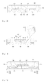
- FIGs. 5A to 5C are views illustrating a process of forming the conductive adhesive of FIG. 4A .
- the first portion 321 of the conductive adhesive is applied to the second lead frame 220b and the second portion 322 of the conductive adhesive is applied to the second electrode 244b.
- a height h 3 and width W 1 of the first portion 321 may be greater than a height h 4 and width W 2 of the second portion 322.
- the size of the first portion 321 may be greater than the size of the second portion 322 because the second portion 322 on the second electrode 244b will be bonded to the first portion 321 on the second lead frame 220b.
- the volume, i.e. the height h 3 and width W 1 of the first portion 331 are greater than the volume, i.e. the height h 4 and width W 2 of the second portion 322, in order to stably support the light emitting device in a bonding process of FIG. 5B .
- voids may be generated in the first portion 321 and the second portion 322. Specifically, the voids may be generated near the surface as illustrated when temperature drops.
- first portion 321 and the second portion 322 may be bonded to each other as the first portion 321 and the second portion 322 are fused and coupled to each other.
- the first portion 321 and the second portion 322 may have the smaller heights h 3 , and h 4 , than the heights h 3 and h 4 of FIG. 5A and the widths W 1 and W 2 equal to the widths of FIG. 5A during coupling or fusion thereof.
- the overlying light emitting device receives force such as, for example, gravity applied toward the underlying first and second lead frames during the coupling or fusion of the first portion 321 and the second portion 322, the heights h 3 , and h 4 , may be smaller than the heights h 3 and h 4 of FIG. 5A and the widths W 1 and W 2 may be equal to the widths of FIG. 5A .
- FIG. 5C illustrates the conductive adhesive 320 after the coupling of the first portion 321 and the second portion 322 ends, and the conductive adhesive 320 may have the same shape as the conductive adhesive 320 of FIG. 4A .
- first portion 321 and the second portion 322 are coupled to each other and an interface between the first portion 321 and the second portion 322 may be a central region having the smallest width W 0 .
- the conductive adhesive more particularly, the central region thereof may have a void-free structure.
- the conductive adhesive is configured as two separate portions in the above-described process, the conductive adhesive may be divided into three or more portions, which may increase the height of the conductive adhesive and reduce transfer of stress to the light emitting device.
- the light emitting device package manufactured by the above-described process may achieve improved bonding reliability because the first portion applied to the lead frame and the second portion applied to the electrode are coupled to each other to form the conductive adhesive.
- the light emitting device package manufactured by the above-described process may achieve improved luminous efficacy owing to removal of voids in the conductive adhesive and may reduce shock transferred to the light emitting structure formed of a GaN based material because the conductive adhesive, which consists of two portions and has a greater thickness than that of the related art, can alleviate stress caused by use of materials having differential thermal expansion coefficients.
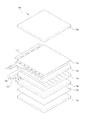
- FIG. 6 is a plan view illustrating a second embodiment of a light emitting device package.
- FIG. 6 illustrates an upper surface of the light emitting device package.
- FIG. 7 is a cross sectional view taken along line A-A' of the light emitting device package illustrated in FIG. 6 .
- the light emitting device package may include a package body 430, a light emitting device 420, a first lead frame 410a, a second lead frame 410b, and conductive adhesives 450.
- the package body 430 may have a cavity 440 and at least one recess 460 formed in the bottom of the cavity 440.
- the package body 430 may be formed of a silicon material or a synthetic resin material, and may be formed of a thermosetting resin.
- the thermosetting resin may be an Epoxy Molding Compound (EMC).
- EMC Epoxy Molding Compound
- enhanced luminous intensity may be accomplished via increase in the reflectivity of light emitted from the light emitting device 420.
- the cavity 440 of the package body 430 may be defined by the bottom and the sidewall.
- the package body 430 may include a first region 430a that defines the sidewall and a portion of the bottom of the cavity 440 and a second region 430b between the first lead frame 410a and the second lead frame 410b.
- the cavity 440 may have a circular shape, an oval shape, or a polygonal shape (e.g., a rectangular shape) when viewed from the top.
- the cavity 440 may have curved corners, and the sidewall of the cavity 440 may be perpendicular to or tilted relative to the bottom of the cavity 440.
- the sidewall of the cavity 440 serves as a reflective surface to reflect light emitted from the light emitting device 420 toward the upper surface of the light emitting device package.
- a separate reflective member (not illustrated) may be provided on the bottom of the cavity 440 to reflect light emitted from the light emitting device 420 so as to luminous efficacy, without being limited thereto.
- the recess 460 may be formed in the bottom of the cavity 440 defined in the package body 430.
- the recess 460 may be disposed at the center of the cavity 440.
- the light emitting device 420 may be placed at the recess 460 and may be disposed above the recess 460.
- the first lead frame 410a and the second lead frame 410b may be spaced apart from each other in the horizontal direction, different from the thickness direction of the package body 430, in the recess 460.
- the first lead frame 410a and the second lead frame 410b may include metal substrates and serve to support the light emitting device 420 disposed on the first and second lead frames 410a and 410b and to transmit electrical signals to the light emitting device 420.
- the first lead frame 410a and the second lead frame 410b may be formed of, for example, copper (Cu), aluminum (Al), silver (Ag), nickel (Ni) or titanium (Ti) and have a single-layer or multi-layer form, without being limited thereto.
- the first lead frame 410a and the second lead frame 410b may be spaced apart from each other by a distance d2 of 0.1 mm or more in the horizontal direction.
- a distance d2 of 0.1 mm or more in the horizontal direction.
- the conductive adhesives 450 formed on the respective lead frames 410 are disposed close to each other, which may cause electrical short-circuit.
- the first lead frame 410a and the second lead frame 410b may outwardly radiate heat generated in the light emitting device 420 and reflect light emitted from the light emitting device 420 so as to increase luminous efficacy.
- a separate reflective member (not illustrated) may be disposed on the first lead frame 410a and the second lead frame 410b to reflect light emitted from the light emitting device 420 so as to increase luminous efficacy, without being limited thereto.
- the conductive adhesives 450 may be disposed between the light emitting device 420 and the first and second lead frames 410a and 410b.
- the conductive adhesives 450 may function to bond the light emitting device 420 and the first and second lead frames 410a and 410b to each other and to electrically connect the same to an external circuit.
- the conductive adhesives 450 may have a first height h2-a.
- the conductive adhesives 450 may comprise a solder paste consisting of a flux serving as a solvent and conductive powder.
- the first height h2-a of the conductive adhesives 450 may vary according to the viscosity of the solder paste and the amount of the flux.
- the first height h2-a may be within a range of 30 ⁇ m to 100 ⁇ m and, more particularly, within a range of 30 ⁇ m to 50 ⁇ m.
- the conductive adhesive 450 serve to bond the lead frames 410a and 410b and the light emitting device 420 to each other and may have the best adhesion when the thickness thereof is within a range of 30 ⁇ m to 50 ⁇ m after removal of the flux serving as a solvent. When the thickness of the conductive adhesives 450 is below 30 ⁇ m, the conductive adhesives 450 cannot achieve required adhesion. When the thickness of the conductive adhesives 450 exceeds 100 ⁇ m, the light emitting device 420 may deviate from a fixed position thereof in a reflow process after application of the solder paste.
- a height h1-a of the recess 460 may be within a range of 30 ⁇ m to 100 ⁇ m.
- the recess 460 cannot prevent the solder paste from flowing to the periphery of the light emitting device 420 upon formation of the conductive adhesives 450.
- the depth h1-a of the recess 460 exceeds 100 ⁇ m, the depth h1-a of the recess 460 may be greater than the height h2-a of the conductive adhesives 450, which makes it impossible for the conductive adhesives 450 to connect the light emitting device 420 and the first and second lead frames 410 to each other.
- a first width w1-a of the recess 460 in the horizontal direction may be 0.9 times or more and 1.1 times or less of a second width w2-a of the light emitting device 420 in the horizontal direction.
- the first width w1-a of the recess 460 in the horizontal direction may be smaller than the second width w2-a of the light emitting device in the horizontal direction, and the first width w1-a may be at least 0.9 times or more of the second width w2-a.
- the conductive adhesives 450 may be reduced in cross sectional area as compared to the light emitting device 420, which may deteriorate adhesion strength between the light emitting device 420 and the first and second lead frames 410.
- FIG. 8 is a plan view illustrating a third embodiment of a light emitting device package
- FIG. 9 is a plan view illustrating a fourth embodiment of a light emitting device package
- FIG. 10 is a plan view illustrating a fifth embodiment of a light emitting device package.
- a first width w1-b of the recess 460 may be greater than a second width w2-b of the light emitting device 420 and the first width w1-b may be at most 1.1 times or less.
- the first width w1-b of the recess 460 is greater than the second width w2-b of the light emitting device 420, more particularly, the first width w1-b exceeds 1.1 times of the second width w2-b, the area of the conductive adhesive 450 exposed around the light emitting device 420 is increased, which may deteriorate luminous efficacy.
- a first virtual vertical line extending from the side edge of the light emitting device 420 in the thickness direction of the light emitting device 420 may overlap with a second virtual vertical line extending from the boundary of the recess 460 in the thickness direction.
- the light emitting device 420 and the recess 460 may have the same horizontal width.
- the cavity 440 may have a first bottom surface 445a provided with the recess 460 and a second bottom surface 445b adjacent to the first bottom surface 445a.
- the first bottom surface 445a may be a bottom surface of the recess 460.
- the conductive adhesives 450 may be disposed on the first bottom surface 445a.
- the first lead frame 410a and the second lead frame 410b may penetrate the package body 430 in the thickness direction and be exposed from a portion of the first bottom surface 445a.
- the first lead frame 410a and the second lead frame 410b may be spaced apart from each other so as to be electrically separated from each other.
- the first lead frame 410a and the second lead frame 410b may be separated from each other by the second region 430b of the package body 430.
- first lead frame 410a and the second lead frame 410b may be horizontally spaced apart from the boundary between the first bottom surface 445 and the second bottom surface 445b to thereby be exposed.
- the recess 460 may be defined by a stepped portion between the first bottom surface 445a and the second bottom surface 445b and the stepped portion may be formed at a region of the package body 430 of the bottom surface of the cavity 440.
- the stepped portion formed at the package body 430 may be acquired by injection molding such that a portion of the first region 430a of the package body 430 corresponding to the second bottom surface 445b of the cavity 440 is disposed higher than the remaining portion.
- the boundary between the first bottom surface 445a and the second bottom surface 445b may contact with the exposed first and second lead frames 410a and 410b.
- the side portion of the first lead frame 410a adjacent to the first region 430a of the package body 430 may contact with the boundary between the first bottom surface 445a and the second bottom surface 445b. That is, the stepped portion between the first bottom surface 445a and the second bottom surface 445b defining the recess 460 in the embodiment of FIG. 9 may be formed at a plane where the first region 430a of the package body 430 contacts with the first lead frame 410a and the second lead frame 410b.
- the recess 460 defined by the stepped portion between the first bottom surface 445a and the second bottom surface 445b may be formed such that the first and second lead frames 410 corresponding to the first bottom surface 445a and the second region 430b of the package body 430 are disposed lower than the second bottom surface 445b.
- the first bottom surface 445a of the cavity 440 may include a first region 445a-1 corresponding to the second region 430b of the package body between the first lead frame 410a and the second lead frame 410b and the remaining second region 445a-2 except for the first region 445a-1.
- the first region 445a-1 of the first bottom surface 445a may protrude than the second region 445a-2.
- a protruding height h3-a of the first region 445a-1 from the second region 445a-2 may be within a range of 30 ⁇ m to 100 ⁇ m.
- the protruding height h3-a is below 30 ⁇ m, this may cause insufficient separation of the conductive adhesives 450 formed respectively on the first lead frame 410a and the second lead frame 410b.
- the protruding height h3-a exceeds 100 ⁇ m, scattering or absorption of light emitted from the light emitting device 430 may occur, thus causing deterioration in luminous efficacy.
- the light emitting device package manufactured by the above-described process may include the recess formed in the bottom of the cavity to prevent the conductive adhesives from flowing out of the recess and from protruding to the periphery of the light emitting device, which may reduce light loss of the package.
- FIG. 11 is a plan view illustrating a sixth embodiment of a light emitting device package.
- the light emitting device package may include a package body 530, a light emitting device 520, a first lead frame 510a, a second lead frame 510b, and conductive adhesives 550.
- the package body 530 may have a cavity 540 and at least one recess 560 formed in the bottom of the cavity 540.
- the package body 530 may be formed of a silicon material or a synthetic resin material, and may be formed of a thermosetting resin.
- the thermosetting resin may be an Epoxy Molding Compound (EMC).
- EMC Epoxy Molding Compound
- enhanced luminous intensity may be accomplished via increase in the reflectivity of light emitted from the light emitting device 520.
- the cavity 540 of the package body 530 may be defined by the bottom and the sidewall.
- the package body 530 may include a first region 530a that defines the sidewall and a portion of the bottom of the cavity 540 and a second region 530b between the first lead frame 510a and the second lead frame 510b.
- the cavity 540 may have a circular shape, an oval shape, or a polygonal shape (e.g., a rectangular shape) when viewed from the top.
- the cavity 540 may have curved corners, and the sidewall of the cavity 440 may be perpendicular to or tilted relative to the bottom of the cavity 440.
- the sidewall of the cavity 540 serves as a reflective surface to reflect light emitted from the light emitting device 520 toward the upper surface of the light emitting device package.
- a separate reflective member (not illustrated) may be provided on the bottom of the cavity 540 to reflect light emitted from the light emitting device 520 so as to luminous efficacy, without being limited thereto.
- the recess 560 may be formed in the bottom of the cavity 540 defined in the package body 530.
- the recess 560 may be disposed at the center of the cavity 540.
- the light emitting device 520 may be placed at the recess 560 and may be disposed above the recess 560.
- the first lead frame 510a and the second lead frame 510b may be spaced apart from each other in the horizontal direction, different from the thickness direction of the package body 530, in the recess 560.
- the conductive adhesives 550 may be disposed between the light emitting device 520 and the first and second lead frames 510a and 510b.
- the conductive adhesives 550 may function to bond the light emitting device 520 and the first and second lead frames 510a and 510b to each other and to electrically connect the same to an external circuit.
- the conductive adhesives 550 may be formed of a conductive material such as, for example, silver (Ag), gold (Au) or a solder.
- each conductive adhesive 550 may have a central region as illustrated and be divided into a first portion and a second portion with the central region disposed therebetween.
- the central region of the conductive adhesive 550 may have the smallest width.
- the width may mean a diameter when the conductive adhesives 550 have a circular horizontal cross section and may mean a length when the conductive adhesives 550 have a square horizontal cross section.
- the conductive adhesives may have a shape or structure as illustrated in FIGs. 4A to 5C and be disposed between the light emitting device and the first and second lead frames.
- the conductive adhesives of the embodiments illustrated in FIGs. 7 to 11 are illustrated as the width of contact surfaces of the conductive adhesives contacting with the first lead frame and the second lead frame being equal to the width of the first lead frame and the second lead frame, as exemplarily illustrated in FIGs. 4A to 5C
- the conductive adhesives may be disposed such that the width of contact surfaces of the conductive adhesives contacting with the first lead frame and the second lead frame is smaller than the width of the first lead frame and the second lead frame.
- the light emitting device packages of the embodiments may have a flip chip bonding structure.
- the light emitting device packages as described above include a recess formed in the bottom of a cavity to prevent a conductive adhesive from flowing out of the recess and protruding to the periphery of a light emitting device, which may reduce light loss of the package.
- light emitting device packages as described above may achieve improved bonding reliability owing to the smallest width of a central region of the conductive adhesive disposed between a lead frame and an electrode of the light emitting device, may achieve enhanced luminous efficacy through removal of voids in the conductive adhesive, and may reduce shock transferred to a light emitting structure formed of a GaN based material because the conductive adhesive, which consists of two portions and has a greater thickness than that of the related art, can alleviate stress caused by use of materials having differential thermal expansion coefficients.
- FIG. 12 is a view illustrating one embodiment of the image display apparatus.
- the image display apparatus 700 of the present embodiment includes a light source module, a reflector 720 on a bottom cover 710, a light guide panel 740 disposed in front of the reflector 720 to guide light, emitted from the light source module, forward of the image display apparatus 700, a first prism sheet 750 and a second prism sheet 760 disposed in front of the light guide panel 740, a panel 770 disposed in front of the second prism sheet 760, and a color filter 780 disposed in front of the panel 770.
- the light source module includes a light emitting device package 735 on a circuit board 730.
- the circuit board 730 may be a PCB, for example, and the light emitting device package 735 is as described above.
- the bottom cover 710 may receive constituent elements of the image display apparatus 700.
- the reflector 720 may be a separate element as exemplarily illustrated in FIG. 12 , or may be a high reflectivity material coated on a back surface of the light guide panel 740 or a front surface of the bottom cover 710.
- the reflector 720 may be formed of a material which has high reflectivity and is formed into an ultra thin shape.
- the reflector 720 may be formed of polyethylene terephthalate (PET).
- the light guide panel 740 may scatter light emitted from the light module to allow the light to be uniformly distributed throughout the entire screen of the image display apparatus 700.
- the light guide panel 740 may be formed of a material having a good index of refraction and light transmissivity, for example, polymethylmethacrylate (PMMA), polycarbonate (PC), or polyethylene (PE).
- PMMA polymethylmethacrylate
- PC polycarbonate
- PE polyethylene
- an air guide type display apparatus may be implemented.
- the first prism sheet 750 includes a support film and a light-transmitting elastic polymer material formed on one surface of the support film.
- the polymer material may form a prism layer in which a plurality of 3-dimensional patterns is repeated.
- the plurality of patterns may be stripe patterns consisting of ridges and valleys repeatedly formed as illustrated.
- the direction of ridges and valleys formed on one surface of the support film of the second prism sheet 760 may be perpendicular to the direction of the ridges and valleys formed on one surface of the support film of the first prism sheet 750. This allows light transmitted from the light source module and the reflector to be uniformly distributed throughout the panel 770.
- the first prism sheet 750 and the second prism sheet 760 serve as optical sheets.
- a micro-lens array, a combination of a diffusive sheet and a micro-lens array, or a combination of a single prism sheet and a micro-lens array may be provided.
- the panel 770 may be a liquid crystal display panel, or may be other kinds of display devices requiring a light source.
- the panel 770 includes liquid crystals disposed between glass bodies, and a polarizer is disposed on either glass body for utilization of polarity of light.
- the liquid crystals have intermediate properties between liquid and solid, and are organic molecules having fluidity like a liquid.
- the panel 770 displays an image using properties of liquid crystals in which a regular molecular arrangement is changed by an external electric field.
- the liquid crystal display panel used in the display apparatus is an active matrix type and employs a transistor as a switch to regulate voltage to be supplied to each pixel.
- the color filter 780 may be disposed on a front surface of the panel 770 to transmit only red, green, and blue light on a per pixel basis among the light emitted from the panel 770, thereby enabling display of an image.
- FIG. 13 is a view illustrating one embodiment of a lighting apparatus including a light emitting device package.
- the lighting apparatus of the present embodiment may include a cover 1100, a light source module 1200, a radiator 1400, a power supply unit 1600, an inner case 1700, and a socket 1800.
- the lighting apparatus according to the present embodiment may further include at least one of a member 1300 and a holder 1500, and the light source module 1200 may include the light emitting device package according to the above described embodiments.
- the cover 1100 may take the form of a hollow bulb or semi-sphere having an opening.
- the cover 1100 and the light source module 1200 may be optically coupled to each other.
- the cover 1100 may diffuse, scatter, or excite light emitted from the light source module 1200.
- the cover 1100 may be an optical member.
- the cover 1100 may be coupled to the radiator 1400, and may have a coupling portion for coupling with the radiator 1400.
- An inner surface of the cover 1100 may be coated with an ivory white paint.
- the ivory white paint may contain a diffuser to diffuse light.
- the surface roughness of the inner surface of the cover 1100 may be greater than the surface roughness of an outer surface of the cover 1100. This serves to sufficiently scatter and diffuse light emitted from the light source module 1200 so as to emit the light to the outside.
- the cover 1100 may be formed of glass, plastic, polypropylene (PP), polyethylene (PE), and polycarbonate (PC), for example.
- polycarbonate is advantageous to achieve excellent light-resistance, heat-resistance, and mechanical strength.
- the cover 1100 may be transparent such that the light source module 1200 can be seen from the outside, or may be opaque.
- the cover 1100 may be formed via blow molding.
- the light source module 1200 may be disposed on a surface of the radiator 1400. Thus, heat from the light source module 1200 is transferred to the radiator 1400.
- the light source module 1200 may include a plurality of light emitting device packages 1210, connection plates 1230, and a connector 1250.
- the member 1300 is disposed on an upper surface of the radiator 1400, and has guide recesses 1310 for insertion of the light emitting device packages 1210 and the connector 1250.
- the guide recesses 1310 correspond to boards of the light emitting device packages 1210 and the connector 1250 in a one to one ratio.
- a reflective material may be applied to or coated over a surface of the member 1300.
- a white paint may be applied to or coated over the surface of the member 1300.
- the member 1300 reflects light, reflected from the inner surface of the cover 1100 to the light source module 1200, to return the light to the cover 1100.
- the lighting apparatus according to the present embodiment may achieve enhanced light efficiency.
- the member 1300 may be formed of an insulating material, for example.
- the connection plates 1230 of the light source module 1200 may be formed of an electrically conductive material. As such, electric contact between the radiator 1400 and the connection plates 1230 may be accomplished.
- the member 1300 may be formed of an insulating material to prevent electrical short-circuit between the connection plates 1230 and the radiator 1400.
- the radiator 1400 may radiate heat from the light source module 1200 and heat from the power supply unit 1600.
- the holder 1500 is configured to close a receiving recess 1719 defined by an insulating portion 1710 of the inner case 1700.
- the power supply unit 1600 received inside the insulating portion 1710 of the inner case 1700, is hermetically sealed.
- the holder 1500 has a guide protrusion 1510.
- the guide protrusion 1510 has a hole for penetration of a protrusion 1610 of the power supply unit 1600.
- the power supply unit 1600 processes or converts an external electrical signal to transmit the same to the light source module 1200.
- the power supply unit 1600 is received in the receiving recess 1719 of the inner case 1700, and is hermetically sealed in the inner case 1700.
- the power supply unit 1600 may include the protrusion 1610, a guide portion 1630, a base 1650, and an extension portion 1670.
- the guide protrusion 1630 is configured to protrude outward from one side of the base 1650.
- the guide portion 1630 may be inserted into the holder 1500.
- a plurality of elements may be disposed on one surface of the base 1650.
- the elements for example, may be a DC converter to convert AC power from an external power source into DC power, a drive chip to control driving of the light source module 1200, and an Electro-Static Discharge prevention element to protect the light source module 1200, but are not limited thereto.
- the extension portion 1670 is configured to protrude outward from the other side of the base 1650.
- the extension portion 1670 is inserted into a connection portion 1750 of the inner case 1700 to receive an electrical signal from an external source.
- the width of the extension portion 1670 may be equal to or less than the width of the connection portion 1750 of the inner case 1700.
- the extension portion 1670 may be electrically connected to one end of a positive electrical wire or a negative electrical wire, and the other end of the positive electrical wire or the negative electrical wire may be electrically connected to the socket 1800.
- the inner case 1700 may include a molding part as well as the power supply unit 1600 therein.
- the molding part is formed of harden molding liquid, and may serve to fix the power supply unit 1600 within the inner case 1700.
- a light emitting device package has the effects of achieving improved bonding reliability because a first portion applied to a lead frame and a second portion applied to an electrode are coupled to each other to form the conductive adhesive, of achieving improved luminous efficacy owing to removal of voids in the conductive adhesive, and of reducing shock transferred to a light emitting structure formed of a GaN based material because the conductive adhesive, which consists of the two portions and has a greater thickness than that of the related art, can alleviate stress caused by use of materials having differential thermal expansion coefficients.
- the light emitting device package has the effect of preventing the conductive adhesives from flowing out of the recess and from protruding to the periphery of a light emitting device, which may reduce light loss of the package.
Priority Applications (1)
| Application Number | Priority Date | Filing Date | Title |
|---|---|---|---|
| EP21207990.9A EP3975272A1 (de) | 2014-05-29 | 2015-05-27 | Gehäuse einer lichtemittierenden vorrichtung |
Applications Claiming Priority (2)
| Application Number | Priority Date | Filing Date | Title |
|---|---|---|---|
| KR1020140064874A KR102194803B1 (ko) | 2014-05-29 | 2014-05-29 | 발광 소자 패키지 |
| KR1020140109575A KR102209035B1 (ko) | 2014-08-22 | 2014-08-22 | 발광소자 패키지 |
Related Child Applications (1)
| Application Number | Title | Priority Date | Filing Date |
|---|---|---|---|
| EP21207990.9A Division EP3975272A1 (de) | 2014-05-29 | 2015-05-27 | Gehäuse einer lichtemittierenden vorrichtung |
Publications (3)
| Publication Number | Publication Date |
|---|---|
| EP2950358A2 true EP2950358A2 (de) | 2015-12-02 |
| EP2950358A3 EP2950358A3 (de) | 2016-01-20 |
| EP2950358B1 EP2950358B1 (de) | 2021-11-17 |
Family
ID=53264552
Family Applications (2)
| Application Number | Title | Priority Date | Filing Date |
|---|---|---|---|
| EP21207990.9A Withdrawn EP3975272A1 (de) | 2014-05-29 | 2015-05-27 | Gehäuse einer lichtemittierenden vorrichtung |
| EP15169338.9A Active EP2950358B1 (de) | 2014-05-29 | 2015-05-27 | Gehäuse für lichtemittierende vorrichtung |
Family Applications Before (1)
| Application Number | Title | Priority Date | Filing Date |
|---|---|---|---|
| EP21207990.9A Withdrawn EP3975272A1 (de) | 2014-05-29 | 2015-05-27 | Gehäuse einer lichtemittierenden vorrichtung |
Country Status (3)
| Country | Link |
|---|---|
| US (1) | US9559278B2 (de) |
| EP (2) | EP3975272A1 (de) |
| CN (1) | CN105304805B (de) |
Cited By (4)
| Publication number | Priority date | Publication date | Assignee | Title |
|---|---|---|---|---|
| CN108598249A (zh) * | 2018-07-24 | 2018-09-28 | 厦门多彩光电子科技有限公司 | 一种led光源的封装方法 |
| KR20190100076A (ko) * | 2018-02-20 | 2019-08-28 | 에피스타 코포레이션 | 발광소자 및 그의 제작방법 |
| EP3734674A4 (de) * | 2017-12-26 | 2021-09-22 | Epistar Corporation | Lichtemittierende vorrichtung und herstellungsverfahren und anzeigemodul dafür |
| EP3806173A4 (de) * | 2018-06-11 | 2022-03-02 | Seoul Semiconductor Co., Ltd. | Lichtemittierendes diodenpaket |
Families Citing this family (17)
| Publication number | Priority date | Publication date | Assignee | Title |
|---|---|---|---|---|
| JPWO2013121708A1 (ja) * | 2012-02-15 | 2015-05-11 | パナソニックIpマネジメント株式会社 | 発光装置およびその製造方法 |
| JP6139444B2 (ja) * | 2014-03-18 | 2017-05-31 | 株式会社東芝 | 磁気抵抗効果素子、磁気抵抗効果素子の製造方法及び磁気メモリ |
| KR102530759B1 (ko) * | 2016-06-14 | 2023-05-11 | 삼성전자주식회사 | 발광소자 패키지 및 그 제조방법 |
| KR20180053489A (ko) * | 2016-11-11 | 2018-05-23 | 삼성전자주식회사 | 발광 소자 패키지 |
| DE102016122810A1 (de) * | 2016-11-25 | 2018-05-30 | Osram Opto Semiconductors Gmbh | Bauteil mit einem lichtemittierenden halbleiterchip |
| JP6936574B2 (ja) * | 2016-12-07 | 2021-09-15 | 日機装株式会社 | 光半導体装置 |
| KR102335216B1 (ko) * | 2017-04-26 | 2021-12-03 | 삼성전자 주식회사 | 발광소자 패키지 |
| US11677059B2 (en) | 2017-04-26 | 2023-06-13 | Samsung Electronics Co., Ltd. | Light-emitting device package including a lead frame |
| US10381534B2 (en) * | 2017-07-18 | 2019-08-13 | Lumileds Llc | Light emitting device including a lead frame and an insulating material |
| CN111357124A (zh) * | 2017-07-18 | 2020-06-30 | 亮锐有限责任公司 | 包括引线框和绝缘材料的发光器件 |
| KR20190019539A (ko) * | 2017-08-18 | 2019-02-27 | 삼성전자주식회사 | 발광 소자 및 발광소자 패키지 |
| KR102641336B1 (ko) * | 2017-09-05 | 2024-02-28 | 쑤저우 레킨 세미컨덕터 컴퍼니 리미티드 | 반도체 소자 패키지 |
| US11355679B2 (en) | 2017-11-01 | 2022-06-07 | Suzhou Lekin Semiconductor Co., Ltd. | Light-emitting device package and lighting source device |
| CN110391321B (zh) * | 2018-04-19 | 2021-05-28 | 展晶科技(深圳)有限公司 | 发光二极管封装体及其制造方法 |
| CN112368850B (zh) * | 2018-12-14 | 2021-06-22 | 新唐科技日本株式会社 | 半导体装置 |
| JP7427888B2 (ja) | 2019-01-31 | 2024-02-06 | 日本電気硝子株式会社 | プリズム、光デバイス、プリズムの製造方法及びパッケージデバイスの製造方法 |
| CN113036016B (zh) * | 2019-12-24 | 2022-10-11 | 群创光电股份有限公司 | 电子装置 |
Family Cites Families (20)
| Publication number | Priority date | Publication date | Assignee | Title |
|---|---|---|---|---|
| US6369451B2 (en) * | 1998-01-13 | 2002-04-09 | Paul T. Lin | Solder balls and columns with stratified underfills on substrate for flip chip joining |
| JP3757881B2 (ja) * | 2002-03-08 | 2006-03-22 | 株式会社日立製作所 | はんだ |
| JP2005011838A (ja) * | 2003-06-16 | 2005-01-13 | Toshiba Corp | 半導体装置及びその組立方法 |
| WO2005093863A1 (en) * | 2004-03-29 | 2005-10-06 | Showa Denko K.K | Compound semiconductor light-emitting device and production method thereof |
| JP4502690B2 (ja) * | 2004-04-13 | 2010-07-14 | 富士通株式会社 | 実装基板 |
| US7378297B2 (en) * | 2004-07-01 | 2008-05-27 | Interuniversitair Microelektronica Centrum (Imec) | Methods of bonding two semiconductor devices |
| TW200729540A (en) * | 2006-01-27 | 2007-08-01 | San-Bao Lin | Improvement of brightness for light-emitting device |
| CN101350321A (zh) * | 2007-07-18 | 2009-01-21 | 晶科电子(广州)有限公司 | 直接倒装于支架内的发光二极管的制造方法 |
| US7847399B2 (en) * | 2007-12-07 | 2010-12-07 | Texas Instruments Incorporated | Semiconductor device having solder-free gold bump contacts for stability in repeated temperature cycles |
| US20090200663A1 (en) * | 2008-02-11 | 2009-08-13 | Daubenspeck Timothy H | Polymer and solder pillars for connecting chip and carrier |
| US7642128B1 (en) * | 2008-12-12 | 2010-01-05 | Stats Chippac, Ltd. | Semiconductor device and method of forming a vertical interconnect structure for 3-D FO-WLCSP |
| US8198131B2 (en) * | 2009-11-18 | 2012-06-12 | Advanced Semiconductor Engineering, Inc. | Stackable semiconductor device packages |
| CN102593012B (zh) * | 2011-01-14 | 2014-12-10 | 株式会社东芝 | 半导体装置的制造方法 |
| US8952402B2 (en) * | 2011-08-26 | 2015-02-10 | Micron Technology, Inc. | Solid-state radiation transducer devices having flip-chip mounted solid-state radiation transducers and associated systems and methods |
| KR101979942B1 (ko) * | 2012-01-03 | 2019-05-17 | 엘지이노텍 주식회사 | 발광 소자 패키지 및 이를 구비한 조명 시스템 |
| KR101926531B1 (ko) * | 2012-05-24 | 2018-12-10 | 엘지이노텍 주식회사 | 발광 소자, 발광 소자 제조방법 및 조명 시스템 |
| US9236524B2 (en) * | 2012-07-18 | 2016-01-12 | Semicon Light Co., Ltd. | Method of manufacturing semiconductor light emitting device |
| JP6032414B2 (ja) * | 2012-11-16 | 2016-11-30 | 東芝ライテック株式会社 | 発光モジュール |
| US9318674B2 (en) * | 2013-02-05 | 2016-04-19 | Cree, Inc. | Submount-free light emitting diode (LED) components and methods of fabricating same |
| US9527723B2 (en) * | 2014-03-13 | 2016-12-27 | STATS ChipPAC Pte. Ltd. | Semiconductor device and method of forming microelectromechanical systems (MEMS) package |
-
2015
- 2015-05-27 EP EP21207990.9A patent/EP3975272A1/de not_active Withdrawn
- 2015-05-27 EP EP15169338.9A patent/EP2950358B1/de active Active
- 2015-05-28 US US14/724,090 patent/US9559278B2/en active Active
- 2015-05-29 CN CN201510289268.6A patent/CN105304805B/zh active Active
Non-Patent Citations (1)
| Title |
|---|
| None |
Cited By (4)
| Publication number | Priority date | Publication date | Assignee | Title |
|---|---|---|---|---|
| EP3734674A4 (de) * | 2017-12-26 | 2021-09-22 | Epistar Corporation | Lichtemittierende vorrichtung und herstellungsverfahren und anzeigemodul dafür |
| KR20190100076A (ko) * | 2018-02-20 | 2019-08-28 | 에피스타 코포레이션 | 발광소자 및 그의 제작방법 |
| EP3806173A4 (de) * | 2018-06-11 | 2022-03-02 | Seoul Semiconductor Co., Ltd. | Lichtemittierendes diodenpaket |
| CN108598249A (zh) * | 2018-07-24 | 2018-09-28 | 厦门多彩光电子科技有限公司 | 一种led光源的封装方法 |
Also Published As
| Publication number | Publication date |
|---|---|
| EP3975272A1 (de) | 2022-03-30 |
| US20150349225A1 (en) | 2015-12-03 |
| EP2950358A3 (de) | 2016-01-20 |
| CN105304805A (zh) | 2016-02-03 |
| US9559278B2 (en) | 2017-01-31 |
| EP2950358B1 (de) | 2021-11-17 |
| CN105304805B (zh) | 2019-02-19 |
Similar Documents
| Publication | Publication Date | Title |
|---|---|---|
| EP2950358B1 (de) | Gehäuse für lichtemittierende vorrichtung | |
| US9882104B2 (en) | Light emitting device package having LED disposed in lead frame cavities | |
| KR102197082B1 (ko) | 발광 소자 및 이를 포함하는 발광소자 패키지 | |
| US9620691B2 (en) | Light emitting device package | |
| JP2021500735A (ja) | 発光素子パッケージ及びこれを含む照明装置 | |
| US9627596B2 (en) | Light emitting device, light emitting device package including the device and lighting apparatus including the package | |
| TWI778103B (zh) | 發光裝置封裝 | |
| CN102376853A (zh) | 发光器件和具有该发光器件的照明系统 | |
| US9768363B2 (en) | Light emitting device module | |
| EP2803715A1 (de) | Phosphor und lichtemittierendes Vorrichtungsgehäuse damit | |
| KR101916144B1 (ko) | 발광소자, 발광소자 패키지 및 라이트 유닛 | |
| KR20140097898A (ko) | 발광소자 | |
| KR102194803B1 (ko) | 발광 소자 패키지 | |
| KR102209035B1 (ko) | 발광소자 패키지 | |
| KR102252475B1 (ko) | 발광 소자 모듈 | |
| KR102163987B1 (ko) | 발광소자 | |
| KR20140099075A (ko) | 발광소자 | |
| KR101865942B1 (ko) | 발광소자, 발광소자 패키지 및 라이트 유닛 | |
| KR20150019490A (ko) | 발광소자 모듈 | |
| KR101959756B1 (ko) | 발광 소자 및 이를 구비한 조명 장치 | |
| KR101896691B1 (ko) | 발광 소자 및 조명 시스템 | |
| KR20180068907A (ko) | 발광소자, 발광소자 패키지 및 라이트 유닛 | |
| KR20150060264A (ko) | 발광소자 | |
| KR20160065597A (ko) | 발광 소자 패키지 | |
| KR20140050284A (ko) | 발광소자, 발광소자 패키지 및 라이트 유닛 |
Legal Events
| Date | Code | Title | Description |
|---|---|---|---|
| AK | Designated contracting states |
Kind code of ref document: A2 Designated state(s): AL AT BE BG CH CY CZ DE DK EE ES FI FR GB GR HR HU IE IS IT LI LT LU LV MC MK MT NL NO PL PT RO RS SE SI SK SM TR |
|
| AX | Request for extension of the european patent |
Extension state: BA ME |
|
| PUAI | Public reference made under article 153(3) epc to a published international application that has entered the european phase |
Free format text: ORIGINAL CODE: 0009012 |
|
| PUAL | Search report despatched |
Free format text: ORIGINAL CODE: 0009013 |
|
| AK | Designated contracting states |
Kind code of ref document: A3 Designated state(s): AL AT BE BG CH CY CZ DE DK EE ES FI FR GB GR HR HU IE IS IT LI LT LU LV MC MK MT NL NO PL PT RO RS SE SI SK SM TR |
|
| AX | Request for extension of the european patent |
Extension state: BA ME |
|
| RIC1 | Information provided on ipc code assigned before grant |
Ipc: H01L 33/48 20100101ALN20151217BHEP Ipc: H01L 23/48 20060101ALI20151217BHEP Ipc: H01L 33/62 20100101AFI20151217BHEP Ipc: H01L 33/64 20100101ALN20151217BHEP |
|
| 17P | Request for examination filed |
Effective date: 20160719 |
|
| RBV | Designated contracting states (corrected) |
Designated state(s): AL AT BE BG CH CY CZ DE DK EE ES FI FR GB GR HR HU IE IS IT LI LT LU LV MC MK MT NL NO PL PT RO RS SE SI SK SM TR |
|
| RAP1 | Party data changed (applicant data changed or rights of an application transferred) |
Owner name: LG INNOTEK CO., LTD. |
|
| STAA | Information on the status of an ep patent application or granted ep patent |
Free format text: STATUS: EXAMINATION IS IN PROGRESS |
|
| 17Q | First examination report despatched |
Effective date: 20200406 |
|
| STAA | Information on the status of an ep patent application or granted ep patent |
Free format text: STATUS: EXAMINATION IS IN PROGRESS |
|
| GRAP | Despatch of communication of intention to grant a patent |
Free format text: ORIGINAL CODE: EPIDOSNIGR1 |
|
| STAA | Information on the status of an ep patent application or granted ep patent |
Free format text: STATUS: GRANT OF PATENT IS INTENDED |
|
| RIC1 | Information provided on ipc code assigned before grant |
Ipc: H01L 33/62 20100101AFI20210628BHEP Ipc: H01L 23/48 20060101ALI20210628BHEP Ipc: H01L 33/48 20100101ALN20210628BHEP Ipc: H01L 33/64 20100101ALN20210628BHEP |
|
| INTG | Intention to grant announced |
Effective date: 20210712 |
|
| RAP1 | Party data changed (applicant data changed or rights of an application transferred) |
Owner name: SUZHOU LEKIN SEMICONDUCTOR CO., LTD. |
|
| GRAS | Grant fee paid |
Free format text: ORIGINAL CODE: EPIDOSNIGR3 |
|
| GRAA | (expected) grant |
Free format text: ORIGINAL CODE: 0009210 |
|
| STAA | Information on the status of an ep patent application or granted ep patent |
Free format text: STATUS: THE PATENT HAS BEEN GRANTED |
|
| AK | Designated contracting states |
Kind code of ref document: B1 Designated state(s): AL AT BE BG CH CY CZ DE DK EE ES FI FR GB GR HR HU IE IS IT LI LT LU LV MC MK MT NL NO PL PT RO RS SE SI SK SM TR |
|
| REG | Reference to a national code |
Ref country code: GB Ref legal event code: FG4D |
|
| REG | Reference to a national code |
Ref country code: DE Ref legal event code: R096 Ref document number: 602015075027 Country of ref document: DE |
|
| REG | Reference to a national code |
Ref country code: IE Ref legal event code: FG4D |
|
| REG | Reference to a national code |
Ref country code: AT Ref legal event code: REF Ref document number: 1448784 Country of ref document: AT Kind code of ref document: T Effective date: 20211215 |
|
| REG | Reference to a national code |
Ref country code: LT Ref legal event code: MG9D |
|
| REG | Reference to a national code |
Ref country code: NL Ref legal event code: MP Effective date: 20211117 |
|
| REG | Reference to a national code |
Ref country code: AT Ref legal event code: MK05 Ref document number: 1448784 Country of ref document: AT Kind code of ref document: T Effective date: 20211117 |
|
| PG25 | Lapsed in a contracting state [announced via postgrant information from national office to epo] |
Ref country code: RS Free format text: LAPSE BECAUSE OF FAILURE TO SUBMIT A TRANSLATION OF THE DESCRIPTION OR TO PAY THE FEE WITHIN THE PRESCRIBED TIME-LIMIT Effective date: 20211117 Ref country code: LT Free format text: LAPSE BECAUSE OF FAILURE TO SUBMIT A TRANSLATION OF THE DESCRIPTION OR TO PAY THE FEE WITHIN THE PRESCRIBED TIME-LIMIT Effective date: 20211117 Ref country code: FI Free format text: LAPSE BECAUSE OF FAILURE TO SUBMIT A TRANSLATION OF THE DESCRIPTION OR TO PAY THE FEE WITHIN THE PRESCRIBED TIME-LIMIT Effective date: 20211117 Ref country code: BG Free format text: LAPSE BECAUSE OF FAILURE TO SUBMIT A TRANSLATION OF THE DESCRIPTION OR TO PAY THE FEE WITHIN THE PRESCRIBED TIME-LIMIT Effective date: 20220217 Ref country code: AT Free format text: LAPSE BECAUSE OF FAILURE TO SUBMIT A TRANSLATION OF THE DESCRIPTION OR TO PAY THE FEE WITHIN THE PRESCRIBED TIME-LIMIT Effective date: 20211117 |
|
| PG25 | Lapsed in a contracting state [announced via postgrant information from national office to epo] |
Ref country code: IS Free format text: LAPSE BECAUSE OF FAILURE TO SUBMIT A TRANSLATION OF THE DESCRIPTION OR TO PAY THE FEE WITHIN THE PRESCRIBED TIME-LIMIT Effective date: 20220317 Ref country code: SE Free format text: LAPSE BECAUSE OF FAILURE TO SUBMIT A TRANSLATION OF THE DESCRIPTION OR TO PAY THE FEE WITHIN THE PRESCRIBED TIME-LIMIT Effective date: 20211117 Ref country code: PT Free format text: LAPSE BECAUSE OF FAILURE TO SUBMIT A TRANSLATION OF THE DESCRIPTION OR TO PAY THE FEE WITHIN THE PRESCRIBED TIME-LIMIT Effective date: 20220317 Ref country code: PL Free format text: LAPSE BECAUSE OF FAILURE TO SUBMIT A TRANSLATION OF THE DESCRIPTION OR TO PAY THE FEE WITHIN THE PRESCRIBED TIME-LIMIT Effective date: 20211117 Ref country code: NO Free format text: LAPSE BECAUSE OF FAILURE TO SUBMIT A TRANSLATION OF THE DESCRIPTION OR TO PAY THE FEE WITHIN THE PRESCRIBED TIME-LIMIT Effective date: 20220217 Ref country code: NL Free format text: LAPSE BECAUSE OF FAILURE TO SUBMIT A TRANSLATION OF THE DESCRIPTION OR TO PAY THE FEE WITHIN THE PRESCRIBED TIME-LIMIT Effective date: 20211117 Ref country code: LV Free format text: LAPSE BECAUSE OF FAILURE TO SUBMIT A TRANSLATION OF THE DESCRIPTION OR TO PAY THE FEE WITHIN THE PRESCRIBED TIME-LIMIT Effective date: 20211117 Ref country code: HR Free format text: LAPSE BECAUSE OF FAILURE TO SUBMIT A TRANSLATION OF THE DESCRIPTION OR TO PAY THE FEE WITHIN THE PRESCRIBED TIME-LIMIT Effective date: 20211117 Ref country code: GR Free format text: LAPSE BECAUSE OF FAILURE TO SUBMIT A TRANSLATION OF THE DESCRIPTION OR TO PAY THE FEE WITHIN THE PRESCRIBED TIME-LIMIT Effective date: 20220218 Ref country code: ES Free format text: LAPSE BECAUSE OF FAILURE TO SUBMIT A TRANSLATION OF THE DESCRIPTION OR TO PAY THE FEE WITHIN THE PRESCRIBED TIME-LIMIT Effective date: 20211117 |
|
| PG25 | Lapsed in a contracting state [announced via postgrant information from national office to epo] |
Ref country code: SM Free format text: LAPSE BECAUSE OF FAILURE TO SUBMIT A TRANSLATION OF THE DESCRIPTION OR TO PAY THE FEE WITHIN THE PRESCRIBED TIME-LIMIT Effective date: 20211117 Ref country code: SK Free format text: LAPSE BECAUSE OF FAILURE TO SUBMIT A TRANSLATION OF THE DESCRIPTION OR TO PAY THE FEE WITHIN THE PRESCRIBED TIME-LIMIT Effective date: 20211117 Ref country code: RO Free format text: LAPSE BECAUSE OF FAILURE TO SUBMIT A TRANSLATION OF THE DESCRIPTION OR TO PAY THE FEE WITHIN THE PRESCRIBED TIME-LIMIT Effective date: 20211117 Ref country code: EE Free format text: LAPSE BECAUSE OF FAILURE TO SUBMIT A TRANSLATION OF THE DESCRIPTION OR TO PAY THE FEE WITHIN THE PRESCRIBED TIME-LIMIT Effective date: 20211117 Ref country code: DK Free format text: LAPSE BECAUSE OF FAILURE TO SUBMIT A TRANSLATION OF THE DESCRIPTION OR TO PAY THE FEE WITHIN THE PRESCRIBED TIME-LIMIT Effective date: 20211117 Ref country code: CZ Free format text: LAPSE BECAUSE OF FAILURE TO SUBMIT A TRANSLATION OF THE DESCRIPTION OR TO PAY THE FEE WITHIN THE PRESCRIBED TIME-LIMIT Effective date: 20211117 |
|
| PGFP | Annual fee paid to national office [announced via postgrant information from national office to epo] |
Ref country code: FR Payment date: 20220408 Year of fee payment: 8 |
|
| REG | Reference to a national code |
Ref country code: DE Ref legal event code: R097 Ref document number: 602015075027 Country of ref document: DE |
|
| PLBE | No opposition filed within time limit |
Free format text: ORIGINAL CODE: 0009261 |
|
| STAA | Information on the status of an ep patent application or granted ep patent |
Free format text: STATUS: NO OPPOSITION FILED WITHIN TIME LIMIT |
|
| 26N | No opposition filed |
Effective date: 20220818 |
|
| PG25 | Lapsed in a contracting state [announced via postgrant information from national office to epo] |
Ref country code: AL Free format text: LAPSE BECAUSE OF FAILURE TO SUBMIT A TRANSLATION OF THE DESCRIPTION OR TO PAY THE FEE WITHIN THE PRESCRIBED TIME-LIMIT Effective date: 20211117 |
|
| PG25 | Lapsed in a contracting state [announced via postgrant information from national office to epo] |
Ref country code: SI Free format text: LAPSE BECAUSE OF FAILURE TO SUBMIT A TRANSLATION OF THE DESCRIPTION OR TO PAY THE FEE WITHIN THE PRESCRIBED TIME-LIMIT Effective date: 20211117 |
|
| REG | Reference to a national code |
Ref country code: CH Ref legal event code: PL |
|
| REG | Reference to a national code |
Ref country code: BE Ref legal event code: MM Effective date: 20220531 |
|
| PG25 | Lapsed in a contracting state [announced via postgrant information from national office to epo] |
Ref country code: MC Free format text: LAPSE BECAUSE OF FAILURE TO SUBMIT A TRANSLATION OF THE DESCRIPTION OR TO PAY THE FEE WITHIN THE PRESCRIBED TIME-LIMIT Effective date: 20211117 Ref country code: LU Free format text: LAPSE BECAUSE OF NON-PAYMENT OF DUE FEES Effective date: 20220527 Ref country code: LI Free format text: LAPSE BECAUSE OF NON-PAYMENT OF DUE FEES Effective date: 20220531 Ref country code: CH Free format text: LAPSE BECAUSE OF NON-PAYMENT OF DUE FEES Effective date: 20220531 |
|
| PG25 | Lapsed in a contracting state [announced via postgrant information from national office to epo] |
Ref country code: IE Free format text: LAPSE BECAUSE OF NON-PAYMENT OF DUE FEES Effective date: 20220527 |
|
| PG25 | Lapsed in a contracting state [announced via postgrant information from national office to epo] |
Ref country code: IT Free format text: LAPSE BECAUSE OF FAILURE TO SUBMIT A TRANSLATION OF THE DESCRIPTION OR TO PAY THE FEE WITHIN THE PRESCRIBED TIME-LIMIT Effective date: 20211117 Ref country code: BE Free format text: LAPSE BECAUSE OF NON-PAYMENT OF DUE FEES Effective date: 20220531 |
|
| PGFP | Annual fee paid to national office [announced via postgrant information from national office to epo] |
Ref country code: DE Payment date: 20230404 Year of fee payment: 9 |
|
| PGFP | Annual fee paid to national office [announced via postgrant information from national office to epo] |
Ref country code: GB Payment date: 20230406 Year of fee payment: 9 |
|
| PG25 | Lapsed in a contracting state [announced via postgrant information from national office to epo] |
Ref country code: HU Free format text: LAPSE BECAUSE OF FAILURE TO SUBMIT A TRANSLATION OF THE DESCRIPTION OR TO PAY THE FEE WITHIN THE PRESCRIBED TIME-LIMIT; INVALID AB INITIO Effective date: 20150527 |
|
| PG25 | Lapsed in a contracting state [announced via postgrant information from national office to epo] |
Ref country code: MK Free format text: LAPSE BECAUSE OF FAILURE TO SUBMIT A TRANSLATION OF THE DESCRIPTION OR TO PAY THE FEE WITHIN THE PRESCRIBED TIME-LIMIT Effective date: 20211117 Ref country code: CY Free format text: LAPSE BECAUSE OF FAILURE TO SUBMIT A TRANSLATION OF THE DESCRIPTION OR TO PAY THE FEE WITHIN THE PRESCRIBED TIME-LIMIT Effective date: 20211117 |