CN111357124A - 包括引线框和绝缘材料的发光器件 - Google Patents
包括引线框和绝缘材料的发光器件 Download PDFInfo
- Publication number
- CN111357124A CN111357124A CN201880060567.4A CN201880060567A CN111357124A CN 111357124 A CN111357124 A CN 111357124A CN 201880060567 A CN201880060567 A CN 201880060567A CN 111357124 A CN111357124 A CN 111357124A
- Authority
- CN
- China
- Prior art keywords
- leadframe
- molding
- led
- post
- package
- Prior art date
- Legal status (The legal status is an assumption and is not a legal conclusion. Google has not performed a legal analysis and makes no representation as to the accuracy of the status listed.)
- Pending
Links
- 239000011810 insulating material Substances 0.000 title description 2
- 238000000465 moulding Methods 0.000 claims abstract description 46
- 239000000463 material Substances 0.000 claims description 37
- 229910052751 metal Inorganic materials 0.000 claims description 25
- 239000002184 metal Substances 0.000 claims description 25
- 238000000034 method Methods 0.000 claims description 17
- 239000008393 encapsulating agent Substances 0.000 claims description 12
- 238000007747 plating Methods 0.000 claims description 9
- 229920001296 polysiloxane Polymers 0.000 claims description 6
- 230000008878 coupling Effects 0.000 claims description 5
- 238000010168 coupling process Methods 0.000 claims description 5
- 238000005859 coupling reaction Methods 0.000 claims description 5
- 239000012777 electrically insulating material Substances 0.000 claims description 2
- 229910052709 silver Inorganic materials 0.000 abstract description 23
- 239000004332 silver Substances 0.000 abstract description 23
- 238000002845 discoloration Methods 0.000 abstract description 8
- 239000004020 conductor Substances 0.000 abstract description 6
- BQCADISMDOOEFD-UHFFFAOYSA-N Silver Chemical compound [Ag] BQCADISMDOOEFD-UHFFFAOYSA-N 0.000 description 22
- 239000012811 non-conductive material Substances 0.000 description 6
- 230000003287 optical effect Effects 0.000 description 6
- 150000001875 compounds Chemical class 0.000 description 5
- 239000012778 molding material Substances 0.000 description 5
- 238000002310 reflectometry Methods 0.000 description 5
- PXHVJJICTQNCMI-UHFFFAOYSA-N Nickel Chemical compound [Ni] PXHVJJICTQNCMI-UHFFFAOYSA-N 0.000 description 4
- KDLHZDBZIXYQEI-UHFFFAOYSA-N Palladium Chemical compound [Pd] KDLHZDBZIXYQEI-UHFFFAOYSA-N 0.000 description 4
- MWUXSHHQAYIFBG-UHFFFAOYSA-N nitrogen oxide Inorganic materials O=[N] MWUXSHHQAYIFBG-UHFFFAOYSA-N 0.000 description 3
- 239000000565 sealant Substances 0.000 description 3
- 239000004065 semiconductor Substances 0.000 description 3
- 239000004593 Epoxy Substances 0.000 description 2
- GQPLMRYTRLFLPF-UHFFFAOYSA-N Nitrous Oxide Chemical compound [O-][N+]#N GQPLMRYTRLFLPF-UHFFFAOYSA-N 0.000 description 2
- CBENFWSGALASAD-UHFFFAOYSA-N Ozone Chemical compound [O-][O+]=O CBENFWSGALASAD-UHFFFAOYSA-N 0.000 description 2
- RAHZWNYVWXNFOC-UHFFFAOYSA-N Sulphur dioxide Chemical compound O=S=O RAHZWNYVWXNFOC-UHFFFAOYSA-N 0.000 description 2
- QVGXLLKOCUKJST-UHFFFAOYSA-N atomic oxygen Chemical compound [O] QVGXLLKOCUKJST-UHFFFAOYSA-N 0.000 description 2
- 239000003086 colorant Substances 0.000 description 2
- 239000002131 composite material Substances 0.000 description 2
- 239000000945 filler Substances 0.000 description 2
- 230000006870 function Effects 0.000 description 2
- PCHJSUWPFVWCPO-UHFFFAOYSA-N gold Chemical compound [Au] PCHJSUWPFVWCPO-UHFFFAOYSA-N 0.000 description 2
- 229910052737 gold Inorganic materials 0.000 description 2
- 239000010931 gold Substances 0.000 description 2
- 238000004519 manufacturing process Methods 0.000 description 2
- 238000001465 metallisation Methods 0.000 description 2
- 239000000203 mixture Substances 0.000 description 2
- 229910052759 nickel Inorganic materials 0.000 description 2
- 238000001579 optical reflectometry Methods 0.000 description 2
- 239000001301 oxygen Substances 0.000 description 2
- 229910052760 oxygen Inorganic materials 0.000 description 2
- 229910052763 palladium Inorganic materials 0.000 description 2
- 230000000704 physical effect Effects 0.000 description 2
- -1 polysiloxanes Polymers 0.000 description 2
- 238000012545 processing Methods 0.000 description 2
- 239000003566 sealing material Substances 0.000 description 2
- NDVLTYZPCACLMA-UHFFFAOYSA-N silver oxide Chemical compound [O-2].[Ag+].[Ag+] NDVLTYZPCACLMA-UHFFFAOYSA-N 0.000 description 2
- 239000007787 solid Substances 0.000 description 2
- 238000003860 storage Methods 0.000 description 2
- 229920001187 thermosetting polymer Polymers 0.000 description 2
- XLYOFNOQVPJJNP-UHFFFAOYSA-N water Chemical compound O XLYOFNOQVPJJNP-UHFFFAOYSA-N 0.000 description 2
- ZAMOUSCENKQFHK-UHFFFAOYSA-N Chlorine atom Chemical compound [Cl] ZAMOUSCENKQFHK-UHFFFAOYSA-N 0.000 description 1
- RYGMFSIKBFXOCR-UHFFFAOYSA-N Copper Chemical compound [Cu] RYGMFSIKBFXOCR-UHFFFAOYSA-N 0.000 description 1
- RWSOTUBLDIXVET-UHFFFAOYSA-N Dihydrogen sulfide Chemical compound S RWSOTUBLDIXVET-UHFFFAOYSA-N 0.000 description 1
- 229920000106 Liquid crystal polymer Polymers 0.000 description 1
- 239000004977 Liquid-crystal polymers (LCPs) Substances 0.000 description 1
- NINIDFKCEFEMDL-UHFFFAOYSA-N Sulfur Chemical compound [S] NINIDFKCEFEMDL-UHFFFAOYSA-N 0.000 description 1
- 229910052946 acanthite Inorganic materials 0.000 description 1
- 229910045601 alloy Inorganic materials 0.000 description 1
- 239000000956 alloy Substances 0.000 description 1
- 238000000149 argon plasma sintering Methods 0.000 description 1
- 239000010953 base metal Substances 0.000 description 1
- 230000008901 benefit Effects 0.000 description 1
- 230000015572 biosynthetic process Effects 0.000 description 1
- 238000005422 blasting Methods 0.000 description 1
- 238000003486 chemical etching Methods 0.000 description 1
- 238000006243 chemical reaction Methods 0.000 description 1
- 239000003795 chemical substances by application Substances 0.000 description 1
- 239000000460 chlorine Substances 0.000 description 1
- 229910052801 chlorine Inorganic materials 0.000 description 1
- 238000004140 cleaning Methods 0.000 description 1
- 238000004590 computer program Methods 0.000 description 1
- 239000000356 contaminant Substances 0.000 description 1
- 229910052802 copper Inorganic materials 0.000 description 1
- 239000010949 copper Substances 0.000 description 1
- 230000000593 degrading effect Effects 0.000 description 1
- 230000009977 dual effect Effects 0.000 description 1
- 238000005868 electrolysis reaction Methods 0.000 description 1
- 238000009713 electroplating Methods 0.000 description 1
- 238000005538 encapsulation Methods 0.000 description 1
- 230000007613 environmental effect Effects 0.000 description 1
- 229920006336 epoxy molding compound Polymers 0.000 description 1
- 238000005530 etching Methods 0.000 description 1
- 230000008020 evaporation Effects 0.000 description 1
- 238000001704 evaporation Methods 0.000 description 1
- 239000007789 gas Substances 0.000 description 1
- 229910052736 halogen Inorganic materials 0.000 description 1
- 150000002367 halogens Chemical class 0.000 description 1
- 229910000037 hydrogen sulfide Inorganic materials 0.000 description 1
- 238000001746 injection moulding Methods 0.000 description 1
- 229910010272 inorganic material Inorganic materials 0.000 description 1
- 239000011147 inorganic material Substances 0.000 description 1
- 239000012212 insulator Substances 0.000 description 1
- 239000007788 liquid Substances 0.000 description 1
- 239000007769 metal material Substances 0.000 description 1
- 150000002739 metals Chemical class 0.000 description 1
- 238000012986 modification Methods 0.000 description 1
- 230000004048 modification Effects 0.000 description 1
- 239000001272 nitrous oxide Substances 0.000 description 1
- 239000011368 organic material Substances 0.000 description 1
- 238000004806 packaging method and process Methods 0.000 description 1
- 239000004033 plastic Substances 0.000 description 1
- 229920000642 polymer Polymers 0.000 description 1
- 239000002952 polymeric resin Substances 0.000 description 1
- 238000004080 punching Methods 0.000 description 1
- 238000007493 shaping process Methods 0.000 description 1
- 239000002210 silicon-based material Substances 0.000 description 1
- 229910001923 silver oxide Inorganic materials 0.000 description 1
- XUARKZBEFFVFRG-UHFFFAOYSA-N silver sulfide Chemical compound [S-2].[Ag+].[Ag+] XUARKZBEFFVFRG-UHFFFAOYSA-N 0.000 description 1
- 229940056910 silver sulfide Drugs 0.000 description 1
- 229910000679 solder Inorganic materials 0.000 description 1
- 238000005476 soldering Methods 0.000 description 1
- 238000004544 sputter deposition Methods 0.000 description 1
- 239000000758 substrate Substances 0.000 description 1
- 229910052717 sulfur Inorganic materials 0.000 description 1
- 239000011593 sulfur Substances 0.000 description 1
- 229920003002 synthetic resin Polymers 0.000 description 1
- KKEYFWRCBNTPAC-UHFFFAOYSA-L terephthalate(2-) Chemical compound [O-]C(=O)C1=CC=C(C([O-])=O)C=C1 KKEYFWRCBNTPAC-UHFFFAOYSA-L 0.000 description 1
- 239000012815 thermoplastic material Substances 0.000 description 1
- 238000001721 transfer moulding Methods 0.000 description 1
- 239000012780 transparent material Substances 0.000 description 1
- 238000004383 yellowing Methods 0.000 description 1
- 239000011787 zinc oxide Substances 0.000 description 1
Images


Classifications
-
- H—ELECTRICITY
- H01—ELECTRIC ELEMENTS
- H01L—SEMICONDUCTOR DEVICES NOT COVERED BY CLASS H10
- H01L33/00—Semiconductor devices having potential barriers specially adapted for light emission; Processes or apparatus specially adapted for the manufacture or treatment thereof or of parts thereof; Details thereof
- H01L33/48—Semiconductor devices having potential barriers specially adapted for light emission; Processes or apparatus specially adapted for the manufacture or treatment thereof or of parts thereof; Details thereof characterised by the semiconductor body packages
- H01L33/62—Arrangements for conducting electric current to or from the semiconductor body, e.g. lead-frames, wire-bonds or solder balls
-
- H—ELECTRICITY
- H01—ELECTRIC ELEMENTS
- H01L—SEMICONDUCTOR DEVICES NOT COVERED BY CLASS H10
- H01L23/00—Details of semiconductor or other solid state devices
- H01L23/48—Arrangements for conducting electric current to or from the solid state body in operation, e.g. leads, terminal arrangements ; Selection of materials therefor
- H01L23/482—Arrangements for conducting electric current to or from the solid state body in operation, e.g. leads, terminal arrangements ; Selection of materials therefor consisting of lead-in layers inseparably applied to the semiconductor body
- H01L23/485—Arrangements for conducting electric current to or from the solid state body in operation, e.g. leads, terminal arrangements ; Selection of materials therefor consisting of lead-in layers inseparably applied to the semiconductor body consisting of layered constructions comprising conductive layers and insulating layers, e.g. planar contacts
-
- H—ELECTRICITY
- H01—ELECTRIC ELEMENTS
- H01L—SEMICONDUCTOR DEVICES NOT COVERED BY CLASS H10
- H01L23/00—Details of semiconductor or other solid state devices
- H01L23/48—Arrangements for conducting electric current to or from the solid state body in operation, e.g. leads, terminal arrangements ; Selection of materials therefor
- H01L23/488—Arrangements for conducting electric current to or from the solid state body in operation, e.g. leads, terminal arrangements ; Selection of materials therefor consisting of soldered or bonded constructions
- H01L23/495—Lead-frames or other flat leads
- H01L23/49541—Geometry of the lead-frame
-
- H—ELECTRICITY
- H01—ELECTRIC ELEMENTS
- H01L—SEMICONDUCTOR DEVICES NOT COVERED BY CLASS H10
- H01L33/00—Semiconductor devices having potential barriers specially adapted for light emission; Processes or apparatus specially adapted for the manufacture or treatment thereof or of parts thereof; Details thereof
- H01L33/48—Semiconductor devices having potential barriers specially adapted for light emission; Processes or apparatus specially adapted for the manufacture or treatment thereof or of parts thereof; Details thereof characterised by the semiconductor body packages
- H01L33/483—Containers
- H01L33/486—Containers adapted for surface mounting
-
- H—ELECTRICITY
- H01—ELECTRIC ELEMENTS
- H01L—SEMICONDUCTOR DEVICES NOT COVERED BY CLASS H10
- H01L33/00—Semiconductor devices having potential barriers specially adapted for light emission; Processes or apparatus specially adapted for the manufacture or treatment thereof or of parts thereof; Details thereof
- H01L33/48—Semiconductor devices having potential barriers specially adapted for light emission; Processes or apparatus specially adapted for the manufacture or treatment thereof or of parts thereof; Details thereof characterised by the semiconductor body packages
- H01L33/52—Encapsulations
- H01L33/54—Encapsulations having a particular shape
-
- H—ELECTRICITY
- H01—ELECTRIC ELEMENTS
- H01L—SEMICONDUCTOR DEVICES NOT COVERED BY CLASS H10
- H01L33/00—Semiconductor devices having potential barriers specially adapted for light emission; Processes or apparatus specially adapted for the manufacture or treatment thereof or of parts thereof; Details thereof
- H01L33/48—Semiconductor devices having potential barriers specially adapted for light emission; Processes or apparatus specially adapted for the manufacture or treatment thereof or of parts thereof; Details thereof characterised by the semiconductor body packages
- H01L33/58—Optical field-shaping elements
- H01L33/60—Reflective elements
-
- H—ELECTRICITY
- H01—ELECTRIC ELEMENTS
- H01L—SEMICONDUCTOR DEVICES NOT COVERED BY CLASS H10
- H01L2224/00—Indexing scheme for arrangements for connecting or disconnecting semiconductor or solid-state bodies and methods related thereto as covered by H01L24/00
- H01L2224/01—Means for bonding being attached to, or being formed on, the surface to be connected, e.g. chip-to-package, die-attach, "first-level" interconnects; Manufacturing methods related thereto
- H01L2224/10—Bump connectors; Manufacturing methods related thereto
- H01L2224/15—Structure, shape, material or disposition of the bump connectors after the connecting process
- H01L2224/16—Structure, shape, material or disposition of the bump connectors after the connecting process of an individual bump connector
- H01L2224/161—Disposition
- H01L2224/16151—Disposition the bump connector connecting between a semiconductor or solid-state body and an item not being a semiconductor or solid-state body, e.g. chip-to-substrate, chip-to-passive
- H01L2224/16221—Disposition the bump connector connecting between a semiconductor or solid-state body and an item not being a semiconductor or solid-state body, e.g. chip-to-substrate, chip-to-passive the body and the item being stacked
- H01L2224/16245—Disposition the bump connector connecting between a semiconductor or solid-state body and an item not being a semiconductor or solid-state body, e.g. chip-to-substrate, chip-to-passive the body and the item being stacked the item being metallic
-
- H—ELECTRICITY
- H01—ELECTRIC ELEMENTS
- H01L—SEMICONDUCTOR DEVICES NOT COVERED BY CLASS H10
- H01L2224/00—Indexing scheme for arrangements for connecting or disconnecting semiconductor or solid-state bodies and methods related thereto as covered by H01L24/00
- H01L2224/01—Means for bonding being attached to, or being formed on, the surface to be connected, e.g. chip-to-package, die-attach, "first-level" interconnects; Manufacturing methods related thereto
- H01L2224/26—Layer connectors, e.g. plate connectors, solder or adhesive layers; Manufacturing methods related thereto
- H01L2224/31—Structure, shape, material or disposition of the layer connectors after the connecting process
- H01L2224/32—Structure, shape, material or disposition of the layer connectors after the connecting process of an individual layer connector
- H01L2224/321—Disposition
- H01L2224/32151—Disposition the layer connector connecting between a semiconductor or solid-state body and an item not being a semiconductor or solid-state body, e.g. chip-to-substrate, chip-to-passive
- H01L2224/32221—Disposition the layer connector connecting between a semiconductor or solid-state body and an item not being a semiconductor or solid-state body, e.g. chip-to-substrate, chip-to-passive the body and the item being stacked
- H01L2224/32245—Disposition the layer connector connecting between a semiconductor or solid-state body and an item not being a semiconductor or solid-state body, e.g. chip-to-substrate, chip-to-passive the body and the item being stacked the item being metallic
-
- H—ELECTRICITY
- H01—ELECTRIC ELEMENTS
- H01L—SEMICONDUCTOR DEVICES NOT COVERED BY CLASS H10
- H01L2224/00—Indexing scheme for arrangements for connecting or disconnecting semiconductor or solid-state bodies and methods related thereto as covered by H01L24/00
- H01L2224/01—Means for bonding being attached to, or being formed on, the surface to be connected, e.g. chip-to-package, die-attach, "first-level" interconnects; Manufacturing methods related thereto
- H01L2224/42—Wire connectors; Manufacturing methods related thereto
- H01L2224/47—Structure, shape, material or disposition of the wire connectors after the connecting process
- H01L2224/48—Structure, shape, material or disposition of the wire connectors after the connecting process of an individual wire connector
- H01L2224/481—Disposition
- H01L2224/48151—Connecting between a semiconductor or solid-state body and an item not being a semiconductor or solid-state body, e.g. chip-to-substrate, chip-to-passive
- H01L2224/48221—Connecting between a semiconductor or solid-state body and an item not being a semiconductor or solid-state body, e.g. chip-to-substrate, chip-to-passive the body and the item being stacked
- H01L2224/48245—Connecting between a semiconductor or solid-state body and an item not being a semiconductor or solid-state body, e.g. chip-to-substrate, chip-to-passive the body and the item being stacked the item being metallic
- H01L2224/48247—Connecting between a semiconductor or solid-state body and an item not being a semiconductor or solid-state body, e.g. chip-to-substrate, chip-to-passive the body and the item being stacked the item being metallic connecting the wire to a bond pad of the item
-
- H—ELECTRICITY
- H01—ELECTRIC ELEMENTS
- H01L—SEMICONDUCTOR DEVICES NOT COVERED BY CLASS H10
- H01L2224/00—Indexing scheme for arrangements for connecting or disconnecting semiconductor or solid-state bodies and methods related thereto as covered by H01L24/00
- H01L2224/01—Means for bonding being attached to, or being formed on, the surface to be connected, e.g. chip-to-package, die-attach, "first-level" interconnects; Manufacturing methods related thereto
- H01L2224/42—Wire connectors; Manufacturing methods related thereto
- H01L2224/47—Structure, shape, material or disposition of the wire connectors after the connecting process
- H01L2224/48—Structure, shape, material or disposition of the wire connectors after the connecting process of an individual wire connector
- H01L2224/481—Disposition
- H01L2224/48151—Connecting between a semiconductor or solid-state body and an item not being a semiconductor or solid-state body, e.g. chip-to-substrate, chip-to-passive
- H01L2224/48221—Connecting between a semiconductor or solid-state body and an item not being a semiconductor or solid-state body, e.g. chip-to-substrate, chip-to-passive the body and the item being stacked
- H01L2224/48245—Connecting between a semiconductor or solid-state body and an item not being a semiconductor or solid-state body, e.g. chip-to-substrate, chip-to-passive the body and the item being stacked the item being metallic
- H01L2224/48257—Connecting between a semiconductor or solid-state body and an item not being a semiconductor or solid-state body, e.g. chip-to-substrate, chip-to-passive the body and the item being stacked the item being metallic connecting the wire to a die pad of the item
-
- H—ELECTRICITY
- H01—ELECTRIC ELEMENTS
- H01L—SEMICONDUCTOR DEVICES NOT COVERED BY CLASS H10
- H01L2224/00—Indexing scheme for arrangements for connecting or disconnecting semiconductor or solid-state bodies and methods related thereto as covered by H01L24/00
- H01L2224/01—Means for bonding being attached to, or being formed on, the surface to be connected, e.g. chip-to-package, die-attach, "first-level" interconnects; Manufacturing methods related thereto
- H01L2224/42—Wire connectors; Manufacturing methods related thereto
- H01L2224/47—Structure, shape, material or disposition of the wire connectors after the connecting process
- H01L2224/48—Structure, shape, material or disposition of the wire connectors after the connecting process of an individual wire connector
- H01L2224/484—Connecting portions
- H01L2224/48463—Connecting portions the connecting portion on the bonding area of the semiconductor or solid-state body being a ball bond
- H01L2224/48464—Connecting portions the connecting portion on the bonding area of the semiconductor or solid-state body being a ball bond the other connecting portion not on the bonding area also being a ball bond, i.e. ball-to-ball
-
- H—ELECTRICITY
- H01—ELECTRIC ELEMENTS
- H01L—SEMICONDUCTOR DEVICES NOT COVERED BY CLASS H10
- H01L2224/00—Indexing scheme for arrangements for connecting or disconnecting semiconductor or solid-state bodies and methods related thereto as covered by H01L24/00
- H01L2224/73—Means for bonding being of different types provided for in two or more of groups H01L2224/10, H01L2224/18, H01L2224/26, H01L2224/34, H01L2224/42, H01L2224/50, H01L2224/63, H01L2224/71
- H01L2224/732—Location after the connecting process
- H01L2224/73251—Location after the connecting process on different surfaces
- H01L2224/73265—Layer and wire connectors
-
- H—ELECTRICITY
- H01—ELECTRIC ELEMENTS
- H01L—SEMICONDUCTOR DEVICES NOT COVERED BY CLASS H10
- H01L2924/00—Indexing scheme for arrangements or methods for connecting or disconnecting semiconductor or solid-state bodies as covered by H01L24/00
- H01L2924/15—Details of package parts other than the semiconductor or other solid state devices to be connected
- H01L2924/181—Encapsulation
-
- H—ELECTRICITY
- H01—ELECTRIC ELEMENTS
- H01L—SEMICONDUCTOR DEVICES NOT COVERED BY CLASS H10
- H01L2933/00—Details relating to devices covered by the group H01L33/00 but not provided for in its subgroups
- H01L2933/0008—Processes
- H01L2933/0033—Processes relating to semiconductor body packages
-
- H—ELECTRICITY
- H01—ELECTRIC ELEMENTS
- H01L—SEMICONDUCTOR DEVICES NOT COVERED BY CLASS H10
- H01L2933/00—Details relating to devices covered by the group H01L33/00 but not provided for in its subgroups
- H01L2933/0008—Processes
- H01L2933/0033—Processes relating to semiconductor body packages
- H01L2933/0066—Processes relating to semiconductor body packages relating to arrangements for conducting electric current to or from the semiconductor body
Landscapes
- Engineering & Computer Science (AREA)
- Microelectronics & Electronic Packaging (AREA)
- Computer Hardware Design (AREA)
- Power Engineering (AREA)
- Manufacturing & Machinery (AREA)
- Physics & Mathematics (AREA)
- Condensed Matter Physics & Semiconductors (AREA)
- General Physics & Mathematics (AREA)
- Led Device Packages (AREA)
Abstract
用于发光二极管(LED)的封装可以包括引线框、LED以及光学反射但不导电的模制件。引线框可以具有第一引线框部分和与第一引线框部分电隔离的第二引线框部分。每个引线框部分可以具有至少一个升高的柱。模制件可以设置在引线框之上,除了在引线框的柱之上之外。LED可以安装在至少一个柱上并且电耦合到至少一个柱。模制件可以用于比如银的高反射、导电材料的目的,而不经受变色。
Description
相关申请的交叉引用
本申请要求2017年7月18日提交的美国专利申请No. 15/652,603和2017年8月2日提交的欧洲专利申请No. 17184498.8的权益,其内容通过引用在此并入本文。
背景技术
发光二极管(“LED”)是固态器件,其当被提供有电流时发射光。LED封装在相对复杂的包装中,该包装并入不同的材料来为LED提供各种功能。封装中通常使用的一种部件是一层银。银为LED半导体器件提供良好的导电性,同时还提供了良好的光学特性,诸如适当波长的光的反射率和高反射率。然而,即使当被密封材料覆盖时,银也经受变色。
发明内容
发光二极管(LED)封装可以包括引线框,该引线框包括与第二引线框部分电隔离的第一引线框部分。第一引线框部分可以包括第一柱,该第一柱升高到第一引线框部分的下表面上方。第二引线框部分可以包括第二柱,该第二柱升高到第二引线框部分的下表面上方。模制件可以覆盖引线框部分的下表面。第一柱和第二柱的至少一部分可以保持暴露。模制件可以包括高光学反射和电绝缘的材料。LED器件可以仅设置在第二柱之上。第一接触可以形成在LED器件上。第一接触可以经由第一线接合电耦合到第一柱。第二接触可以形成在LED器件上。第二接触可以经由第二线接合电耦合到第二柱。
附图说明
可以从以下结合附图通过示例的方式给出的下列描述中得到更详细的理解,其中附图中相同的附图标记指示相同的元件,并且,在附图中:
图1是根据示例的LED封装的截面图;
图2和3图示了根据示例的LED封装的替代配置;并且
图4-8图示了根据示例的LED封装的分解图和制造方法。
具体实施方式
在下文中将参考附图更全面地描述不同的发光二极管(“LED”)实施方式的示例。这些示例并非互相排斥,并且可以将在一个示例中发现的特征与在一个或多个其他示例中发现的特征相组合以实现附加的实施方式。因此,将理解的是,附图中所示的示例仅出于说明目的而提供,并且它们不意图以任何方式限制本公开。相同的数字始终指代相同的元件。
将理解,尽管术语第一、第二等在本文中可以用于描述各种元件,但是这些元件不应受到这些术语的限制。这些术语仅用于区分一个元件和另一个元件。例如,在不脱离本说明书的范围的情况下,第一元件可以被称为第二元件,并且类似地,第二元件可以被称为第一元件。如本文所使用的,术语“和/或”包括相关联的列出项目中的一个或多个的任何和所有组合。
将理解的是,当诸如层、区域或衬底的元件被称为“在另一元件上”或“延伸到另一元件上”时,其可以直接在另一个元件上或直接延伸到另一个元件上,或者也可以存在中间元件。相反,当一元件被称为“直接在另一元件上”或“直接延伸到另一元件上”时,不存在中间元件。还将理解,当一元件被称为“连接”或“耦合”到另一元件时,其可以直接连接或耦合到另一个元件,或者可以存在中间元件。相反,当一元件被称为“直接连接”或“直接耦合”到另一元件时,不存在中间元件。将理解的是,除了图中描绘的任何取向之外,这些术语意图涵盖元件的不同取向。
在本文中可以使用诸如“在……下方”或“在……上方”或者“在……上”或“在……下”或者“水平”或“竖直”的相对术语来描述如图中所图示的一个元件、层或区域与另一元件、层或区域的关系。将理解,除了图中描绘的取向之外,这些术语意图涵盖器件的不同取向。
在本文中封装被提供具有降低银的使用的必要性的物理特性,该银虽然具有良好的光学质量,诸如反射率,但容易被环境剂变色。更具体地,银对诸如硫化氢、卤素、氧、水蒸气、一氧化二氮、二氧化硫和臭氧的材料具有高亲和力,这些材料可以在受污染的空气中,尤其是在城市中心或工业区中被发现。这些材料可能导致黑色硫化银或深黄色氧化银(称为银变色)的形成,这可能显著且迅速地降低银的反射率。
封装包括:金属引线框,至少部分地设置在引线框上方并形成发光二极管(“LED”)部件设置在其中的阱的模制材料,以及设置在该阱内的密封材料。金属引线框包括柱,其上设置有LED或其他部件和/或其用作电接触点以形成包括引线框和阱内的部件的电路。引线框除柱以外的区域均被光学反射的模制件覆盖。阱内的模制材料的顶表面与柱的顶表面(或在柱上方形成的任何附加层(诸如,镀金属层等)的顶表面)齐平(或近似齐平),以形成阱的单个齐平底表面。模制材料是高反射的材料,用于反射来自LED的光并为LED封装提供良好的光学特性。具有升高的柱的引线框配置允许在LED封装中不使用或者在LED封装中较少使用更常规的材料,比如银,这减轻了银变色的问题。更具体地,尽管在常规设计中,银将覆盖阱的大部分底表面,并因此将经受变色,从而降低了LED封装的光学特性,但是在本公开的封装中,暴露的表面实际上缺少银,反射率是由不经受银变色的反射模制材料提供的。
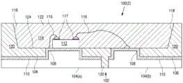
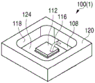
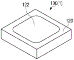
图1是根据示例的封装100(1)的截面图。封装100包括引线框102,该引线框102包括第一引线框部分104(a)和第二引线框部分104(b),第一引线框部分104(a)与第二引线框部分104(b)电隔离。引线框102的不同引线框部分104提供封装100内的部件与封装外部的部件之间的电耦合。例如,一个引线框部分104可以耦合至LED器件112的一个端子和一条外部线,并且另一引线框部分104可以耦合至LED器件112的另一端子和不同的外部线,使得LED器件112被集成到电路中。金属镀层106设置在第一引线框部分104(a)和第二引线框部分104(b)上方,以将诸如LED 112的各种部件电耦合到引线框102。尽管在常规设计中,镀层由银制成,使得镀层可以作为电导体以及光学反射器两者而执行双重任务,但是在本公开中,金属镀层106不需要是银,因为LED封装100的反射率由模制材料120提供。金属镀层106可以是除银以外的任何技术上可行的材料,或者可以是银。
引线框102具有在引线框102的下表面110上方延伸的两个升高部分或“柱”108。柱108用于为阱114内的电气部件(诸如LED 112)提供电接触的点。阱114被由模制化合物制成的模制件120的侧壁118形成。LED 112设置在柱108中的一个上,并且经由线接合116电耦合到第二引线框部分104(b)的柱108。LED 112还经由导电接触113电耦合到第一引线框部分104(a)的柱108。柱108允许在阱114内的部件和引线框102之间形成电连接,同时最小化例如在引线框102之上设置的暴露金属的量。密封剂122设置在阱114内的部件之上,并填充阱114的空间。
在常规的引线框设计中,引线框的两个(或更多个)电隔离部分镀有诸如银的金属材料,该金属材料提供与引线框的电耦合和具有良好颜色特性的反射光的高光学反射率两者。在常规设计中,银非常经常用作特别好的导电和光学反射材料。然而,如上所述,即使在被密封材料覆盖时,银也经受变色。本公开的具有柱108的引线框102提供了以下功能:允许阱114中的部件与引线框102的电连接,同时还允许阱114的大部分最底部的表面(该最底部的表面也称为“盆124”)不包括银,而是替代地包括高光学反射性的非导电材料。注意,盆124包括金属层106的最顶部表面和在阱114的底部处的模制件120的最顶部表面。尽管图示为齐平的表面,但是盆124的各个部分可以略微或基本不平坦。
图2和3图示了根据示例的封装100的替代配置。更具体地,图2图示了封装100(2),其中LED 112经由两个线接合116耦合到引线框102,并且图3图示了封装100(3),其中LED112的底部上的两个接触119将LED 112耦合到引线框102。图2是根据另一示例的封装100(2)的截面图。封装100(2)类似于封装100(1),除了在封装100(2)中,LED 112通过两个线接合116(其通过接触117而耦合到LED 112),而不是通过LED 112底部上的接触113和单个线接合116,耦合到引线框102。LED 112安装在柱108上,但没有通过LED 112的底表面与柱的电耦合。图3是根据又一示例的封装100(3)的截面图。在封装100(3)中,LED 112通过两个接触119耦合到引线框102,并且没有线接合116。LED 112安装在所图示的引线框部分104两者之上,以允许两个接触119耦合到两个引线框部分104,而LED 112直接位于两个引线框部分104之上。
尽管示出了阱114内的部件的特定配置,但是应当理解,未图示出的各种配置在本公开的教导内。盆124的组成根据柱108的形状、大小和数量而变化。在各个实施例中,盆124主要是非导电材料,诸如模制件120的材料。在这样的实施例中,盆124是50%的非导电材料,85%的非导电材料或95%的非导电材料。盆124的不是非导电材料的部分包括引线框102和/或金属层106的导电材料。
在上面图示的示例封装100中,模制件120包括高反射材料。例如,模制件120包括具有高的热、机械、电和光化学稳定性的硅树脂模制化合物,诸如但不限于热固性聚硅氧烷及其衍生化合物。在各种实施例中,模制件120由电绝缘材料形成,该电绝缘材料诸如塑料、热固性材料、热塑性材料、聚合物、环氧聚合物树脂、基于硅树脂的复合材料、复合模制化合物硅树脂、聚环己烯、聚环己烯对苯二甲酸酯、环氧模制化合物、液晶聚合物、其混合物或任何其他合适的材料。形成模制件120的材料可以包括诸如有机或无机材料的填料。填料可以调节模制件120的材料的物理性质,以在LED器件的应用条件下改善材料的完整性和可靠性,并实现模制件120的期望的光学反射率。用于模制件120的材料是耐用的,基本上没有变黄,机械上合适,与适当的制造工艺兼容并且高反射性的。优选地,模制件120具有与引线框102相似的热膨胀系数,其中“相似”是指热膨胀系数彼此在10%之内。尽管上面列出了用于模制件120的某些可能的材料,但是可以使用任何合适的材料。
金属镀层106被图示出设置在引线框102的顶表面之上,但是在各种示例中,金属镀层106仅设置在引线框102的顶表面的一部分之上,诸如在柱108之上。此外,金属镀层106可以是任何导电材料。在一些实施例中,形成盆124的金属镀106和模制件120两者都是这样的材料:在高温下稳定、在高剂量的短波长(蓝和UV)光下稳定,并且对在LED 112的预期应用的环境中的腐蚀性气体(诸如硫和/或其化合物、氯和/或其化合物、氮氧化物、臭氧、水蒸气、氧)和其他污染物呈惰性。尽管示例封装100中的引线框102被图示为具有设置在顶表面之上的金属层106,以提供用于图1和2的线接合116或图3中的接触119的兼容性,以及对引线框102的基底金属的保护。在一些实施例中,例如,当这种兼容性和/或保护不需要时,不存在这种金属层106。
包括柱108的引线框包括导电材料。导电材料可以是例如金属,诸如铜、银、金、镍、钯、其组合、其合金,相同或不同金属的多层堆叠,或任何其他合适的材料。
尽管在一些实施例中图示出了线接合,但是可以使用用于将LED 112电连接到引线框102的任何合适的布置。例如,在所图示的封装100中的任一个中,可以使用(多个)金属桥、焊料、导电环氧树脂或其他合适的连接而不是线接合。
如上所述,在图1-3中,模制件120形成了阱114,各种部件设置在该阱114中。在其他实施例中,使用刚好的形成模制件120的材料来在结构上固定引线框部分104的相对位置而不形成阱114。在其他实施例中,模制件120形成具有浅侧壁118的阱114,例如刚好深到足以容纳LED 112、(多个)线接合116(如果存在)或阱114内的其他部件。
示出了设置在阱114内的密封剂122。在一些实施例中,密封剂122包括透明材料,该透明材料保护LED 112和阱144内的其他部件,诸如线接合116(如果存在)。在一些实施例中,密封剂122包括诸如波长转换材料的材料、改善密封剂122的热性能的材料、引起或减少光散射的材料、充当过滤器的材料或任何其他合适的材料。
尽管描述了LED 112,但是在各种实施例中,LED 112可以被其他类型的发光器件(诸如激光二极管)替代,并且可以使用由其他材料系统(诸如其他III-V族材料、III族磷化物、III族砷化物、II-VI族材料、ZnO或基于Si的材料)制成的半导体发光器件。发射蓝色或UV的发光器件通常与一种或多种波长转换材料组合以产生不同颜色的光,使得来自发光器件和波长转换材料的组合光呈现白色或给定应用所需的任何其他颜色。
图4-8图示了形成图1的封装100(1)的方法,并且还一起图示了图1的封装100(1)的分解图。应当理解,为清楚起见,已经从图4-8中所图示的视图中省略了一些部件。例如,未示出金属层106。
在图4中,形成引线框102。引线框102的在形成模制件120之后暴露的支柱108在比引线框102的其他部分更高的高度处,当形成模制件120时,引线框102的其他部分被模制件120覆盖。可以通过例如通过模制、折叠、冲压、穿孔、蚀刻或任何其他合适的技术来成形金属片来形成引线框。在形成引线框102之后,可以在例如引线框120的整个表面之上或者仅在某些位置之上(诸如在引线框的在形成模制件120之后暴露的部分上)形成金属层106(未示出)。金属层106可以通过电镀、溅射、蒸发或任何其他合适的技术形成。
在图5中,模制件120在引线框120上和周围形成。模制件120可以通过例如模制、注塑成型、传递模制或任何其他合适的技术来形成。可以将模制件120成形为形成侧壁118,该侧壁118形成适于封闭下文描述的在图8中形成的密封剂122的阱114。在形成绝缘体120之后,仅暴露引线框102的部分,诸如柱108。引线框120的其他部分被模制件120覆盖。阱114的大部分底表面(“盆”)124被模制件120覆盖,而不是被柱108覆盖。在形成模制件120之后,可以采取其他处理步骤以暴露区域(诸如,柱108),其在最终器件中不被模制件120覆盖。合适的处理步骤包括湿法或干法喷砂、化学蚀刻、电解或任何其他合适的技术以清洁柱108的表面。在这种清洁之后,其他金属层,诸如银、金、镍、钯或其他合适的材料可以沉积在柱108上。
在图6中,LED 112和任何其他部件(诸如,静电放电保护芯片或任何其他合适的部件)附接到引线框的暴露的柱108。LED 112和其他部件可以通过例如焊接或任何其他合适的技术来附接。
在图7中,如果使用的话,形成一个或多个线接合116。可以形成除了线接合116之外或作为线接合116的替代方案的其他电连接,以提供LED 112和柱108之间的电连接。
在图7中,密封剂122设置在阱114中,从而覆盖LED 112。密封剂122可以通过例如模制、分涂或任何其他合适的技术形成。在一些实施例中,密封剂122以液体或凝胶形式设置在阱114中,然后固化成固体。密封剂122可以包括波长转换材料,以将LED芯片发射的光转换成其他颜色的光。来自LED芯片的光和从波长转换材料发射的光的组合形成LED器件的最终颜色的光。
图1-8中所图示的器件或上述器件中的任一个可以用于任何合适的应用中,诸如例如普通照明,用于显示器的背光或专用照明应用。在一些实施例中,上述器件可以被并入到移动电话中。
已经详细描述了实施例,本领域技术人员将认识到,在给出本公开的情况下,可以进行修改而不背离本文描述的发明构思的精神。特别地,本文描述的不同器件的不同特征和部件可以在其他器件中的任一个中使用,或者特征和部件可以从器件中的任一个省略。在一个实施例的上下文中描述的结构的特征可以适用于任何实施例。因此,无意将说明书的范围限于所图示和描述的具体实施例。
尽管上文以特定组合描述了特征和元件,但是本领域普通技术人员将认识到,每个特征或元件可以单独使用或与其他特征和元件以任何组合使用。另外,本文描述的方法可以在并入计算机可读介质中的计算机程序、软件或固件中实现,以由计算机或处理器执行。计算机可读介质的示例包括电子信号(通过有线或无线连接传输)和计算机可读存储介质。计算机可读存储介质的示例包括但不限于只读存储器(ROM)、随机存取存储器(RAM)、寄存器、高速缓存存储器、半导体存储器器件、诸如内部硬盘和可移动盘的磁介质、磁光介质和诸如CD-ROM盘和数字多功能盘(DVD)的光学介质。
Claims (14)
1.一种发光二极管(LED)封装,包括:
引线框,包括与第二引线框部分电隔离的第一引线框部分,所述第一引线框部分包括第一柱,所述第一柱升高到所述第一引线框部分的下表面上方,并且所述第二引线框部分包括第二柱,所述第二柱升高到所述第二引线框部分的下表面上方;
模制件,覆盖引线框部分的下表面并且暴露所述第一柱和所述第二柱的至少一部分,其中,所述模制件包括高光学反射和电绝缘的材料;
LED器件,仅设置在所述第二柱之上;
形成在所述LED器件上的第一接触,所述第一接触经由第一线接合电耦合到所述第一柱;以及
形成在所述LED器件上的第二接触,所述第二接触经由第二线接合电耦合到所述第二柱。
2.根据权利要求1所述的LED封装,其中:
所述模制件包括侧壁,所述侧壁成形为形成阱。
3.根据权利要求2所述的LED封装,还包括:
设置在所述阱内的密封剂,所述密封剂被配置为物理地保护所述LED器件。
4.根据权利要求1所述的LED封装,其中,所述第二柱具有一宽度,所述宽度大于所述LED器件的宽度。
5.根据权利要求1所述的LED封装,其中,所述模制件包括硅树脂材料。
6.根据权利要求1所述的LED封装,还包括:
电镀金属,设置在所述引线框之上,既在所述模制件之下又在所述第一柱和所述第二柱的暴露的相应表面上。
7.根据权利要求1所述的LED封装,还包括:
电镀金属,设置在所述第一柱和所述第二柱之上,但不在所述模制件之下的所述引线框上。
8.一种形成发光二极管(LED)封装的方法,所述方法包括:
形成引线框,所述引线框包括与第二引线框部分电隔离的第一引线框部分,所述第一引线框部分包括第一柱,所述第一柱升高到所述第一引线框部分的下表面上方,并且所述第二引线框部分包括第二柱,所述第二柱升高到所述第二引线框部分的下表面上方;
在所述引线框上和周围形成模制件,所述模制件覆盖引线框部分的下表面并且暴露所述第一柱和所述第二柱的至少一部分;
仅在所述第二柱上安装LED器件;
经由第一线接合将所述LED器件的第一接触电耦合到所述第一柱;并且
经由第二线接合将所述LED器件的第二接触电耦合到所述第二柱。
9.根据权利要求8所述的方法,其中形成所述模制件包括:
形成所述模制件以包括侧壁,所述侧壁成形为形成阱。
10.根据权利要求9所述的方法,还包括:
在所述阱内设置密封剂,所述密封剂被配置为物理地保护所述LED器件。
11.根据权利要求8所述的方法,其中,所述第二柱具有一宽度,所述宽度大于所述LED器件的宽度。
12.根据权利要求8所述的方法,其中,所述模制件包括硅树脂材料。
13.根据权利要求8所述的方法,还包括:
既在所述模制件之下又在所述第一柱和所述第二柱的暴露的表面上,在所述引线框之上电镀金属。
14.根据权利要求8所述的方法,还包括:
在所述第一柱和所述第二柱之上,但不在所述模制件之下的所述引线框上电镀金属。
Applications Claiming Priority (5)
| Application Number | Priority Date | Filing Date | Title |
|---|---|---|---|
| US15/652,603 US10381534B2 (en) | 2017-07-18 | 2017-07-18 | Light emitting device including a lead frame and an insulating material |
| US15/652603 | 2017-07-18 | ||
| EP17184498.8 | 2017-08-02 | ||
| EP17184498 | 2017-08-02 | ||
| PCT/US2018/041774 WO2019018193A1 (en) | 2017-07-18 | 2018-07-12 | LIGHT EMITTING DEVICE COMPRISING A CONNECTION GRID AND INSULATING MATERIAL |
Publications (1)
| Publication Number | Publication Date |
|---|---|
| CN111357124A true CN111357124A (zh) | 2020-06-30 |
Family
ID=63047471
Family Applications (1)
| Application Number | Title | Priority Date | Filing Date |
|---|---|---|---|
| CN201880060567.4A Pending CN111357124A (zh) | 2017-07-18 | 2018-07-12 | 包括引线框和绝缘材料的发光器件 |
Country Status (6)
| Country | Link |
|---|---|
| EP (1) | EP3656001A1 (zh) |
| JP (2) | JP2020527864A (zh) |
| KR (1) | KR102408302B1 (zh) |
| CN (1) | CN111357124A (zh) |
| TW (1) | TWI832819B (zh) |
| WO (1) | WO2019018193A1 (zh) |
Families Citing this family (4)
| Publication number | Priority date | Publication date | Assignee | Title |
|---|---|---|---|---|
| US11335842B2 (en) * | 2018-02-14 | 2022-05-17 | Maven Optronics Co., Ltd. | Chip-scale packaging light-emitting device with electrode polarity identifier and method of manufacturing the same |
| JP2020167366A (ja) * | 2019-02-26 | 2020-10-08 | ローム株式会社 | 半導体発光装置および半導体発光装置の製造方法 |
| US11393960B2 (en) * | 2019-02-26 | 2022-07-19 | Rohm Co., Ltd. | Semiconductor light-emitting device and method for manufacturing the same |
| CN114628263B (zh) * | 2022-05-13 | 2022-08-05 | 威海三维曲板智能装备有限公司 | 一种光电混合封装结构及其制造方法 |
Citations (9)
| Publication number | Priority date | Publication date | Assignee | Title |
|---|---|---|---|---|
| CN101834258A (zh) * | 2009-03-11 | 2010-09-15 | 索尼公司 | 发光元件的安装用封装、发光装置、背光和液晶显示装置 |
| CN101834256A (zh) * | 2009-03-10 | 2010-09-15 | Lg伊诺特有限公司 | 发光器件封装 |
| JP2013058695A (ja) * | 2011-09-09 | 2013-03-28 | Dainippon Printing Co Ltd | 樹脂付リードフレーム、半導体装置、照明装置、樹脂付リードフレームの製造方法および半導体装置の製造方法 |
| US20130343067A1 (en) * | 2011-02-28 | 2013-12-26 | Nichia Corporation | Light emitting device |
| JP2014031436A (ja) * | 2012-08-03 | 2014-02-20 | Shin Etsu Chem Co Ltd | 硬化性樹脂組成物、その硬化物及びそれを用いた光半導体デバイス |
| CN104247057A (zh) * | 2012-02-27 | 2014-12-24 | Lg伊诺特有限公司 | 发光器件封装 |
| JP2015119011A (ja) * | 2013-12-17 | 2015-06-25 | 日亜化学工業株式会社 | 樹脂パッケージ及び発光装置 |
| US20150349225A1 (en) * | 2014-05-29 | 2015-12-03 | Lg Innotek Co., Ltd. | Light emitting device package |
| CN105830240A (zh) * | 2014-01-07 | 2016-08-03 | 皇家飞利浦有限公司 | 发光器件封装 |
Family Cites Families (17)
| Publication number | Priority date | Publication date | Assignee | Title |
|---|---|---|---|---|
| US3830762A (en) * | 1973-08-24 | 1974-08-20 | Us Agriculture | Polysaccharide-containing elastomers |
| KR100867515B1 (ko) * | 2004-12-06 | 2008-11-07 | 삼성전기주식회사 | 발광소자 패키지 |
| US20070126020A1 (en) * | 2005-12-03 | 2007-06-07 | Cheng Lin | High-power LED chip packaging structure and fabrication method thereof |
| US8044418B2 (en) * | 2006-07-13 | 2011-10-25 | Cree, Inc. | Leadframe-based packages for solid state light emitting devices |
| KR101248051B1 (ko) * | 2008-07-24 | 2013-03-27 | 쿠퍼 타이어 앤드 러버 캄파니 | 실란, 소수성화된 실리카, 실리카 마스터배치 및 고무 제품의 제조방법 |
| US8044420B2 (en) * | 2009-01-15 | 2011-10-25 | Advanced Semiconductor Engineering, Inc. | Light emitting diode package structure |
| JP5509878B2 (ja) * | 2010-01-27 | 2014-06-04 | 凸版印刷株式会社 | Led発光素子用リードフレーム基板の製造方法 |
| US8525213B2 (en) * | 2010-03-30 | 2013-09-03 | Lg Innotek Co., Ltd. | Light emitting device having multiple cavities and light unit having the same |
| JP5618189B2 (ja) * | 2010-07-30 | 2014-11-05 | 大日本印刷株式会社 | 樹脂付リードフレームおよびその製造方法、ならびに半導体装置およびその製造方法 |
| KR101303168B1 (ko) * | 2011-07-26 | 2013-09-09 | 안상정 | 반도체 발광부 연결체 |
| JP2013219104A (ja) * | 2012-04-05 | 2013-10-24 | Toppan Printing Co Ltd | Led用リードフレームおよびその製造方法 |
| CN104124237A (zh) * | 2013-04-26 | 2014-10-29 | 光明半导体(天津)有限公司 | 发光二极管封装件及其制造方法 |
| EP3110878A1 (en) * | 2014-02-27 | 2017-01-04 | E. I. du Pont de Nemours and Company | Micropulp-elastomer masterbatches and compounds based thereon |
| JP6262578B2 (ja) * | 2014-03-18 | 2018-01-17 | スタンレー電気株式会社 | 発光装置 |
| KR102625499B1 (ko) * | 2014-12-22 | 2024-01-17 | 뉴트리션 앤드 바이오사이언시스 유에스에이 4, 인크. | 폴리 알파-1,3-글루칸 함유 폴리머 블렌드 |
| JP6056914B2 (ja) * | 2015-07-07 | 2017-01-11 | 大日本印刷株式会社 | 樹脂付リードフレーム、半導体装置および照明装置 |
| US20200181370A1 (en) * | 2016-10-28 | 2020-06-11 | E I Du Pont De Nemours And Company | Rubber compositions comprising polysaccharides |
-
2018
- 2018-07-12 EP EP18747087.7A patent/EP3656001A1/en active Pending
- 2018-07-12 CN CN201880060567.4A patent/CN111357124A/zh active Pending
- 2018-07-12 JP JP2020502262A patent/JP2020527864A/ja active Pending
- 2018-07-12 WO PCT/US2018/041774 patent/WO2019018193A1/en unknown
- 2018-07-12 KR KR1020207004530A patent/KR102408302B1/ko active IP Right Grant
- 2018-07-18 TW TW107124773A patent/TWI832819B/zh active
-
2023
- 2023-05-10 JP JP2023077765A patent/JP2023090921A/ja active Pending
Patent Citations (9)
| Publication number | Priority date | Publication date | Assignee | Title |
|---|---|---|---|---|
| CN101834256A (zh) * | 2009-03-10 | 2010-09-15 | Lg伊诺特有限公司 | 发光器件封装 |
| CN101834258A (zh) * | 2009-03-11 | 2010-09-15 | 索尼公司 | 发光元件的安装用封装、发光装置、背光和液晶显示装置 |
| US20130343067A1 (en) * | 2011-02-28 | 2013-12-26 | Nichia Corporation | Light emitting device |
| JP2013058695A (ja) * | 2011-09-09 | 2013-03-28 | Dainippon Printing Co Ltd | 樹脂付リードフレーム、半導体装置、照明装置、樹脂付リードフレームの製造方法および半導体装置の製造方法 |
| CN104247057A (zh) * | 2012-02-27 | 2014-12-24 | Lg伊诺特有限公司 | 发光器件封装 |
| JP2014031436A (ja) * | 2012-08-03 | 2014-02-20 | Shin Etsu Chem Co Ltd | 硬化性樹脂組成物、その硬化物及びそれを用いた光半導体デバイス |
| JP2015119011A (ja) * | 2013-12-17 | 2015-06-25 | 日亜化学工業株式会社 | 樹脂パッケージ及び発光装置 |
| CN105830240A (zh) * | 2014-01-07 | 2016-08-03 | 皇家飞利浦有限公司 | 发光器件封装 |
| US20150349225A1 (en) * | 2014-05-29 | 2015-12-03 | Lg Innotek Co., Ltd. | Light emitting device package |
Also Published As
| Publication number | Publication date |
|---|---|
| TWI832819B (zh) | 2024-02-21 |
| JP2020527864A (ja) | 2020-09-10 |
| KR20200033889A (ko) | 2020-03-30 |
| EP3656001A1 (en) | 2020-05-27 |
| TW201916413A (zh) | 2019-04-16 |
| WO2019018193A1 (en) | 2019-01-24 |
| KR102408302B1 (ko) | 2022-06-14 |
| JP2023090921A (ja) | 2023-06-29 |
Similar Documents
| Publication | Publication Date | Title |
|---|---|---|
| US10847680B2 (en) | Light emitting device package | |
| KR102408302B1 (ko) | 리드 프레임 및 절연 재료를 포함하는 발광 디바이스 | |
| KR101760545B1 (ko) | 수지 부착 리드 프레임 및 그 제조 방법, 및 리드 프레임 | |
| US9172015B2 (en) | Light emitting device, light emitting device package, and lighting system | |
| CN101315963B (zh) | 半导体发光装置 | |
| US20180261740A1 (en) | Light emitting device package | |
| JP5922326B2 (ja) | Led用リードフレームまたは基板およびその製造方法、ならびに半導体装置およびその製造方法 | |
| US20110241028A1 (en) | Light emitting device and light unit having the same | |
| US20160118549A1 (en) | Light emitting device package | |
| US20130277701A1 (en) | Package and method for manufacturing package | |
| US8487336B2 (en) | Light emitting device package | |
| US8772793B2 (en) | Light emitting diodes and method for manufacturing the same | |
| CN107735872B (zh) | 发光装置及包括该发光装置的发光装置封装体 | |
| JP2011228687A (ja) | Led用リードフレームまたは基板、半導体装置、およびled用リードフレームまたは基板の製造方法 | |
| US10381534B2 (en) | Light emitting device including a lead frame and an insulating material | |
| US11081630B2 (en) | Light emitting device package with a coating layer | |
| KR101526087B1 (ko) | 광전 소자용 하우징 및 그 하우징의 제조 방법 | |
| KR101956056B1 (ko) | 발광 소자 및 이를 구비한 조명 시스템 | |
| KR101064094B1 (ko) | 발광 소자 패키지 | |
| KR102136373B1 (ko) | 발광소자 패키지용 리드 프레임, 리드 프레임의 제조 방법 및 발광소자 패키지의 제조 방법 | |
| CN111837245A (zh) | 发光器件封装 | |
| KR20150080838A (ko) | 발광소자 |
Legal Events
| Date | Code | Title | Description |
|---|---|---|---|
| PB01 | Publication | ||
| PB01 | Publication | ||
| SE01 | Entry into force of request for substantive examination | ||
| SE01 | Entry into force of request for substantive examination |