EP2937896B1 - Method of transfering a printable semiconductor element - Google Patents
Method of transfering a printable semiconductor element Download PDFInfo
- Publication number
- EP2937896B1 EP2937896B1 EP15163216.3A EP15163216A EP2937896B1 EP 2937896 B1 EP2937896 B1 EP 2937896B1 EP 15163216 A EP15163216 A EP 15163216A EP 2937896 B1 EP2937896 B1 EP 2937896B1
- Authority
- EP
- European Patent Office
- Prior art keywords
- printable semiconductor
- semiconductor element
- wafer
- gaas
- ribbons
- Prior art date
- Legal status (The legal status is an assumption and is not a legal conclusion. Google has not performed a legal analysis and makes no representation as to the accuracy of the status listed.)
- Active
Links
Images


Classifications
-
- H—ELECTRICITY
- H10—SEMICONDUCTOR DEVICES; ELECTRIC SOLID-STATE DEVICES NOT OTHERWISE PROVIDED FOR
- H10P—GENERIC PROCESSES OR APPARATUS FOR THE MANUFACTURE OR TREATMENT OF DEVICES COVERED BY CLASS H10
- H10P14/00—Formation of materials, e.g. in the shape of layers or pillars
- H10P14/40—Formation of materials, e.g. in the shape of layers or pillars of conductive or resistive materials
-
- H—ELECTRICITY
- H10—SEMICONDUCTOR DEVICES; ELECTRIC SOLID-STATE DEVICES NOT OTHERWISE PROVIDED FOR
- H10D—INORGANIC ELECTRIC SEMICONDUCTOR DEVICES
- H10D62/00—Semiconductor bodies, or regions thereof, of devices having potential barriers
- H10D62/10—Shapes, relative sizes or dispositions of the regions of the semiconductor bodies; Shapes of the semiconductor bodies
- H10D62/117—Shapes of semiconductor bodies
- H10D62/118—Nanostructure semiconductor bodies
-
- G—PHYSICS
- G03—PHOTOGRAPHY; CINEMATOGRAPHY; ANALOGOUS TECHNIQUES USING WAVES OTHER THAN OPTICAL WAVES; ELECTROGRAPHY; HOLOGRAPHY
- G03F—PHOTOMECHANICAL PRODUCTION OF TEXTURED OR PATTERNED SURFACES, e.g. FOR PRINTING, FOR PROCESSING OF SEMICONDUCTOR DEVICES; MATERIALS THEREFOR; ORIGINALS THEREFOR; APPARATUS SPECIALLY ADAPTED THEREFOR
- G03F7/00—Photomechanical, e.g. photolithographic, production of textured or patterned surfaces, e.g. printing surfaces; Materials therefor, e.g. comprising photoresists; Apparatus specially adapted therefor
- G03F7/0002—Lithographic processes using patterning methods other than those involving the exposure to radiation, e.g. by stamping
-
- H—ELECTRICITY
- H10—SEMICONDUCTOR DEVICES; ELECTRIC SOLID-STATE DEVICES NOT OTHERWISE PROVIDED FOR
- H10D—INORGANIC ELECTRIC SEMICONDUCTOR DEVICES
- H10D30/00—Field-effect transistors [FET]
- H10D30/01—Manufacture or treatment
- H10D30/021—Manufacture or treatment of FETs having insulated gates [IGFET]
- H10D30/025—Manufacture or treatment of FETs having insulated gates [IGFET] of vertical IGFETs
-
- H—ELECTRICITY
- H10—SEMICONDUCTOR DEVICES; ELECTRIC SOLID-STATE DEVICES NOT OTHERWISE PROVIDED FOR
- H10D—INORGANIC ELECTRIC SEMICONDUCTOR DEVICES
- H10D30/00—Field-effect transistors [FET]
- H10D30/01—Manufacture or treatment
- H10D30/021—Manufacture or treatment of FETs having insulated gates [IGFET]
- H10D30/028—Manufacture or treatment of FETs having insulated gates [IGFET] of double-diffused metal oxide semiconductor [DMOS] FETs
- H10D30/0291—Manufacture or treatment of FETs having insulated gates [IGFET] of double-diffused metal oxide semiconductor [DMOS] FETs of vertical DMOS [VDMOS] FETs
-
- H—ELECTRICITY
- H10—SEMICONDUCTOR DEVICES; ELECTRIC SOLID-STATE DEVICES NOT OTHERWISE PROVIDED FOR
- H10D—INORGANIC ELECTRIC SEMICONDUCTOR DEVICES
- H10D30/00—Field-effect transistors [FET]
- H10D30/01—Manufacture or treatment
- H10D30/021—Manufacture or treatment of FETs having insulated gates [IGFET]
- H10D30/031—Manufacture or treatment of FETs having insulated gates [IGFET] of thin-film transistors [TFT]
-
- H—ELECTRICITY
- H10—SEMICONDUCTOR DEVICES; ELECTRIC SOLID-STATE DEVICES NOT OTHERWISE PROVIDED FOR
- H10D—INORGANIC ELECTRIC SEMICONDUCTOR DEVICES
- H10D30/00—Field-effect transistors [FET]
- H10D30/40—FETs having zero-dimensional [0D], one-dimensional [1D] or two-dimensional [2D] charge carrier gas channels
- H10D30/47—FETs having zero-dimensional [0D], one-dimensional [1D] or two-dimensional [2D] charge carrier gas channels having two-dimensional [2D] charge carrier gas channels, e.g. nanoribbon FETs or high electron mobility transistors [HEMT]
- H10D30/471—High electron mobility transistors [HEMT] or high hole mobility transistors [HHMT]
- H10D30/475—High electron mobility transistors [HEMT] or high hole mobility transistors [HHMT] having wider bandgap layer formed on top of lower bandgap active layer, e.g. undoped barrier HEMTs such as i-AlGaN/GaN HEMTs
-
- H—ELECTRICITY
- H10—SEMICONDUCTOR DEVICES; ELECTRIC SOLID-STATE DEVICES NOT OTHERWISE PROVIDED FOR
- H10D—INORGANIC ELECTRIC SEMICONDUCTOR DEVICES
- H10D30/00—Field-effect transistors [FET]
- H10D30/60—Insulated-gate field-effect transistors [IGFET]
- H10D30/64—Double-diffused metal-oxide semiconductor [DMOS] FETs
- H10D30/66—Vertical DMOS [VDMOS] FETs
-
- H—ELECTRICITY
- H10—SEMICONDUCTOR DEVICES; ELECTRIC SOLID-STATE DEVICES NOT OTHERWISE PROVIDED FOR
- H10D—INORGANIC ELECTRIC SEMICONDUCTOR DEVICES
- H10D30/00—Field-effect transistors [FET]
- H10D30/60—Insulated-gate field-effect transistors [IGFET]
- H10D30/67—Thin-film transistors [TFT]
- H10D30/6757—Thin-film transistors [TFT] characterised by the structure of the channel, e.g. transverse or longitudinal shape or doping profile
-
- H—ELECTRICITY
- H10—SEMICONDUCTOR DEVICES; ELECTRIC SOLID-STATE DEVICES NOT OTHERWISE PROVIDED FOR
- H10D—INORGANIC ELECTRIC SEMICONDUCTOR DEVICES
- H10D62/00—Semiconductor bodies, or regions thereof, of devices having potential barriers
- H10D62/10—Shapes, relative sizes or dispositions of the regions of the semiconductor bodies; Shapes of the semiconductor bodies
- H10D62/117—Shapes of semiconductor bodies
- H10D62/118—Nanostructure semiconductor bodies
- H10D62/119—Nanowire, nanosheet or nanotube semiconductor bodies
- H10D62/121—Nanowire, nanosheet or nanotube semiconductor bodies oriented parallel to substrates
-
- H—ELECTRICITY
- H10—SEMICONDUCTOR DEVICES; ELECTRIC SOLID-STATE DEVICES NOT OTHERWISE PROVIDED FOR
- H10D—INORGANIC ELECTRIC SEMICONDUCTOR DEVICES
- H10D62/00—Semiconductor bodies, or regions thereof, of devices having potential barriers
- H10D62/80—Semiconductor bodies, or regions thereof, of devices having potential barriers characterised by the materials
- H10D62/86—Semiconductor bodies, or regions thereof, of devices having potential barriers characterised by the materials being Group II-VI materials, e.g. ZnO
-
- H—ELECTRICITY
- H10—SEMICONDUCTOR DEVICES; ELECTRIC SOLID-STATE DEVICES NOT OTHERWISE PROVIDED FOR
- H10D—INORGANIC ELECTRIC SEMICONDUCTOR DEVICES
- H10D62/00—Semiconductor bodies, or regions thereof, of devices having potential barriers
- H10D62/80—Semiconductor bodies, or regions thereof, of devices having potential barriers characterised by the materials
- H10D62/881—Semiconductor bodies, or regions thereof, of devices having potential barriers characterised by the materials being a two-dimensional material
- H10D62/882—Graphene
-
- H—ELECTRICITY
- H10—SEMICONDUCTOR DEVICES; ELECTRIC SOLID-STATE DEVICES NOT OTHERWISE PROVIDED FOR
- H10D—INORGANIC ELECTRIC SEMICONDUCTOR DEVICES
- H10D86/00—Integrated devices formed in or on insulating or conducting substrates, e.g. formed in silicon-on-insulator [SOI] substrates or on stainless steel or glass substrates
- H10D86/01—Manufacture or treatment
-
- H—ELECTRICITY
- H10—SEMICONDUCTOR DEVICES; ELECTRIC SOLID-STATE DEVICES NOT OTHERWISE PROVIDED FOR
- H10P—GENERIC PROCESSES OR APPARATUS FOR THE MANUFACTURE OR TREATMENT OF DEVICES COVERED BY CLASS H10
- H10P14/00—Formation of materials, e.g. in the shape of layers or pillars
- H10P14/20—Formation of materials, e.g. in the shape of layers or pillars of semiconductor materials
- H10P14/38—Formation of materials, e.g. in the shape of layers or pillars of semiconductor materials characterised by treatments done after the formation of the materials
- H10P14/3822—Controlling the interface between substrate and epitaxial layer, e.g. by ion implantation followed by annealing
-
- H—ELECTRICITY
- H10—SEMICONDUCTOR DEVICES; ELECTRIC SOLID-STATE DEVICES NOT OTHERWISE PROVIDED FOR
- H10P—GENERIC PROCESSES OR APPARATUS FOR THE MANUFACTURE OR TREATMENT OF DEVICES COVERED BY CLASS H10
- H10P72/00—Handling or holding of wafers, substrates or devices during manufacture or treatment thereof
- H10P72/70—Handling or holding of wafers, substrates or devices during manufacture or treatment thereof for supporting or gripping
- H10P72/74—Handling or holding of wafers, substrates or devices during manufacture or treatment thereof for supporting or gripping using temporarily an auxiliary support
-
- B—PERFORMING OPERATIONS; TRANSPORTING
- B82—NANOTECHNOLOGY
- B82Y—SPECIFIC USES OR APPLICATIONS OF NANOSTRUCTURES; MEASUREMENT OR ANALYSIS OF NANOSTRUCTURES; MANUFACTURE OR TREATMENT OF NANOSTRUCTURES
- B82Y10/00—Nanotechnology for information processing, storage or transmission, e.g. quantum computing or single electron logic
-
- B—PERFORMING OPERATIONS; TRANSPORTING
- B82—NANOTECHNOLOGY
- B82Y—SPECIFIC USES OR APPLICATIONS OF NANOSTRUCTURES; MEASUREMENT OR ANALYSIS OF NANOSTRUCTURES; MANUFACTURE OR TREATMENT OF NANOSTRUCTURES
- B82Y40/00—Manufacture or treatment of nanostructures
-
- H—ELECTRICITY
- H10—SEMICONDUCTOR DEVICES; ELECTRIC SOLID-STATE DEVICES NOT OTHERWISE PROVIDED FOR
- H10D—INORGANIC ELECTRIC SEMICONDUCTOR DEVICES
- H10D62/00—Semiconductor bodies, or regions thereof, of devices having potential barriers
- H10D62/80—Semiconductor bodies, or regions thereof, of devices having potential barriers characterised by the materials
- H10D62/85—Semiconductor bodies, or regions thereof, of devices having potential barriers characterised by the materials being Group III-V materials, e.g. GaAs
- H10D62/8503—Nitride Group III-V materials, e.g. AlN or GaN
-
- H—ELECTRICITY
- H10—SEMICONDUCTOR DEVICES; ELECTRIC SOLID-STATE DEVICES NOT OTHERWISE PROVIDED FOR
- H10D—INORGANIC ELECTRIC SEMICONDUCTOR DEVICES
- H10D86/00—Integrated devices formed in or on insulating or conducting substrates, e.g. formed in silicon-on-insulator [SOI] substrates or on stainless steel or glass substrates
- H10D86/01—Manufacture or treatment
- H10D86/021—Manufacture or treatment of multiple TFTs
- H10D86/0214—Manufacture or treatment of multiple TFTs using temporary substrates
-
- H—ELECTRICITY
- H10—SEMICONDUCTOR DEVICES; ELECTRIC SOLID-STATE DEVICES NOT OTHERWISE PROVIDED FOR
- H10D—INORGANIC ELECTRIC SEMICONDUCTOR DEVICES
- H10D86/00—Integrated devices formed in or on insulating or conducting substrates, e.g. formed in silicon-on-insulator [SOI] substrates or on stainless steel or glass substrates
- H10D86/01—Manufacture or treatment
- H10D86/021—Manufacture or treatment of multiple TFTs
- H10D86/0241—Manufacture or treatment of multiple TFTs using liquid deposition, e.g. printing
-
- H—ELECTRICITY
- H10—SEMICONDUCTOR DEVICES; ELECTRIC SOLID-STATE DEVICES NOT OTHERWISE PROVIDED FOR
- H10P—GENERIC PROCESSES OR APPARATUS FOR THE MANUFACTURE OR TREATMENT OF DEVICES COVERED BY CLASS H10
- H10P72/00—Handling or holding of wafers, substrates or devices during manufacture or treatment thereof
- H10P72/70—Handling or holding of wafers, substrates or devices during manufacture or treatment thereof for supporting or gripping
- H10P72/74—Handling or holding of wafers, substrates or devices during manufacture or treatment thereof for supporting or gripping using temporarily an auxiliary support
- H10P72/7426—Handling or holding of wafers, substrates or devices during manufacture or treatment thereof for supporting or gripping using temporarily an auxiliary support used as a support during build up manufacturing of active devices
-
- H—ELECTRICITY
- H10—SEMICONDUCTOR DEVICES; ELECTRIC SOLID-STATE DEVICES NOT OTHERWISE PROVIDED FOR
- H10P—GENERIC PROCESSES OR APPARATUS FOR THE MANUFACTURE OR TREATMENT OF DEVICES COVERED BY CLASS H10
- H10P72/00—Handling or holding of wafers, substrates or devices during manufacture or treatment thereof
- H10P72/70—Handling or holding of wafers, substrates or devices during manufacture or treatment thereof for supporting or gripping
- H10P72/74—Handling or holding of wafers, substrates or devices during manufacture or treatment thereof for supporting or gripping using temporarily an auxiliary support
- H10P72/7428—Handling or holding of wafers, substrates or devices during manufacture or treatment thereof for supporting or gripping using temporarily an auxiliary support used to support diced chips prior to mounting
-
- H—ELECTRICITY
- H10—SEMICONDUCTOR DEVICES; ELECTRIC SOLID-STATE DEVICES NOT OTHERWISE PROVIDED FOR
- H10P—GENERIC PROCESSES OR APPARATUS FOR THE MANUFACTURE OR TREATMENT OF DEVICES COVERED BY CLASS H10
- H10P72/00—Handling or holding of wafers, substrates or devices during manufacture or treatment thereof
- H10P72/70—Handling or holding of wafers, substrates or devices during manufacture or treatment thereof for supporting or gripping
- H10P72/74—Handling or holding of wafers, substrates or devices during manufacture or treatment thereof for supporting or gripping using temporarily an auxiliary support
- H10P72/7434—Handling or holding of wafers, substrates or devices during manufacture or treatment thereof for supporting or gripping using temporarily an auxiliary support used in a transfer process involving at least two transfer steps, i.e. including an intermediate handle substrate
-
- H—ELECTRICITY
- H10—SEMICONDUCTOR DEVICES; ELECTRIC SOLID-STATE DEVICES NOT OTHERWISE PROVIDED FOR
- H10P—GENERIC PROCESSES OR APPARATUS FOR THE MANUFACTURE OR TREATMENT OF DEVICES COVERED BY CLASS H10
- H10P72/00—Handling or holding of wafers, substrates or devices during manufacture or treatment thereof
- H10P72/70—Handling or holding of wafers, substrates or devices during manufacture or treatment thereof for supporting or gripping
- H10P72/74—Handling or holding of wafers, substrates or devices during manufacture or treatment thereof for supporting or gripping using temporarily an auxiliary support
- H10P72/7438—Handling or holding of wafers, substrates or devices during manufacture or treatment thereof for supporting or gripping using temporarily an auxiliary support with parts of the auxiliary support remaining in the finished device
Definitions
- thin film transistors having semiconductor elements made of these materials exhibit field effect mobilities approximately three orders of magnitude less than complementary single crystalline silicon based devices.
- flexible electronic devices are presently limited to specific applications not requiring high performance, such as use in switching elements for active matrix flat panel displays with non-emissive pixels and in light emitting diodes.
- TFT thin film transistor
- One class of higher performing flexible electronic devices is based on polycrystalline silicon thin film semiconductor elements fabricated by pulse laser annealing of amorphous silicon thin films. While this class of flexible electronic devices provides enhanced device electronic performance characteristics, use of pulsed laser annealing limits the ease and flexibility of fabrication of such devices, thereby significantly increasing costs.
- Another promising new class of higher performing flexible electronic devices is devices that employ solution processable nanoscale materials, such as nanowires, nanoribbons, nanoparticles and carbon nanotubes, as active functional components in a number of macroelectronic and microelectronic devices.
- This device field effect mobility is several orders of magnitude lower than the device field effect mobilities of conventional single crystalline inorganic thin film transistors, and is likely due to practical challenges in aligning, densely packing and electrically contacting discrete nanowires or nanoribbons using the methods and device configurations disclosed in Duan et al.
- Ridley et al. report improved electrical properties relative to comparable devices having organic semiconductor elements, the device mobilities achieved by these techniques ( ⁇ 1 cm 2 V -1 S -1 ) are several orders of magnitude lower than the device field effect mobilities of conventional single crystalline inorganic thin film transistors. Limits on the field effect mobilities achieved by the device configurations and fabrication methods of Ridley et al. are likely to arise from the electrical contact established between individual nanoparticles. Particularly, the use of organic end groups to stabilize nanocrystal solutions and prevent agglomeration may impede establishing good electrical contact between adjacent nanoparticles that is necessary for providing high device field effect mobilities.
- Duan et al. and Ridley et al. provide methods for fabricating thin film transistors on plastic substrates
- the device configurations described employ transistors comprising mechanically rigid device components, such as electrodes, semiconductors and/or dielectrics. Selection of a plastic substrate with good mechanical properties may provide electronic devices capable of performing in flexed or distorted orientations. However, such motion is expected to generate mechanical strain on the individual rigid transistor device components. This mechanical strain may induce damage to individual components, for example by cracking, and also may degrade or disrupt electrical contact between device components.
- U.S. Patents 11/145,574 and 11/145,542 both filed on June 2, 2005 , disclose a high yield fabrication platform using printable semiconductor elements for making electronic devices, optoelectronic devices and other functional electronic assemblies by versatile, low cost and high area printing techniques.
- the disclosed methods and compositions provide for the transfer, assembly and/or and integration of microsized and/or nanosized semiconductor structures using dry transfer contact printing and/or solution printing techniques providing good placement accuracy, registration and pattern fidelity over large substrate areas.
- the disclosed methods provide important processing advantages enabling the integration of high quality semiconductor materials fabricated using conventional high temperature processing methods onto substrates by printing techniques which may be independently carried out at relatively low temperatures ( ⁇ about 400 degrees Celsius) compatible with a range of useful substrate materials, including flexible plastic substrates.
- Flexible thin film transistors fabricated using printable semiconductor materials exhibit good electronic performance characteristics, such as device field effect mobilities greater than 300 cm 2 V -1 s -1 and on/off ratios greater than 10 3 , when in flexed and non-flexed conformations.
- US2004/234231 discloses a method for a three-dimensional structural body which includes sequentially bonding/transferring and laminating plural cross-sectional form members.
- the present invention is set out in the claims.
- the present invention is as follows: a method of transferring a printable semiconductor element (300), said method comprising the steps of:
- Print relates to materials, structures, device components and/or integrated functional devices that are capable of transfer, assembly, patterning, organizing and/or integrating onto or into substrates without exposure of the substrate to high temperatures (i.e. at temperatures less than or equal to about 400 degrees Celsius).
- printable materials, elements, device components and devices are capable of transfer, assembly, patterning, organizing and/or integrating onto or into substrates via solution printing or dry transfer contact printing.
- Print semiconductor elements of the present disclosure comprise semiconductor structures that are able to be assembled and/or integrated onto substrate surfaces, for example using by dry transfer contact printing and/or solution printing methods.
- printable semiconductor elements of the present disclosure are unitary single crystalline, polycrystalline or microcrystalline inorganic semiconductor structures.
- printable semiconductor elements are connected to a substrate, such as a mother wafer, via one or more bridge elements.
- a unitary structure is a monolithic element having features that are mechanically connected.
- Semiconductor elements of the present disclosure may be undoped or doped, may have a selected spatial distribution of dopants and may be doped with a plurality of different dopant materials, including P and N type dopants.
- the present disclosure includes microstructured printable semiconductor elements having at least one cross sectional dimension greater than or equal to about 1 micron and nanostructured printable semiconductor elements having at least one cross sectional dimension less than or equal to about 1 micron.
- Printable semiconductor elements useful in many applications comprises elements derived from "top down" processing of high purity bulk materials, such as high purity crystalline semiconductor wafers generated using conventional high temperature processing techniques.
- printable semiconductor elements of the present disclosure comprise composite structures having a semiconductor operational connected to at least one additional device component or structure, such as a conducting layer, dielectric layer, electrode, additional semiconductor structure or any combination of these.
- printable semiconductor elements of the present disclosure comprise stretchable semiconductor elements and/or heterogeneous semiconductor elements.
- Cross sectional dimension refers to the dimensions of a cross section of device, device component or material.
- Cross sectional dimensions include width, thickness, radius, and diameter.
- printable semiconductor elements having a ribbon shape are characterized by a length and two cross sectional dimensions; thickness and width.
- printable semiconductor elements having a cylindrical shape are characterized by a length and the cross sectional dimension diameter (alternatively radius).
- “Longitudinally oriented in a substantially parallel configuration” refers to an orientation such that the longitudinal axes of a population of elements, such as printable semiconductor elements, are oriented substantially parallel to a selected alignment axis.
- substantially parallel to a selected axis refers to an orientation within 10 degrees of an absolutely parallel orientation, more preferably within 5 degrees of an absolutely parallel orientation.
- a flexible material, structure, device or device component may be deformed into a curved shape without introducing strain larger than or equal to about 5 %, preferably for some applications larger than or equal to about 1 %, and more preferably for some applications larger than or equal to about 0.5 %.
- semiconductor refers to any material that is a material that is an insulator at a very low temperature, but which has a appreciable electrical conductivity at a temperatures of about 300 Kelvin. In the present description, use of the term semiconductor is intended to be consistent with use of this term in the art of microelectronics and electrical devices.
- Semiconductors useful in the present disclosure may comprise element semiconductors, such as silicon, germanium and diamond, and compound semiconductors, such as group IV compound semiconductors such as SiC and SiGe, group III-V semiconductors such as AlSb, AlAs, Aln, AIP, BN, GaSb, GaAs, GaN, GaP, InSb, InAs, InN, and InP, group III-V ternary semiconductors alloys such as Al x Ga 1 - x As, group II-VI semiconductors such as CsSe, CdS, CdTe, ZnO, ZnSe, ZnS, and ZnTe, group I-VII semiconductors CuCI, group IV - VI semiconductors such as PbS, PbTe and SnS, layer semiconductors such as Pbl 2 , MoS 2 and GaSe, oxide semiconductors such as CuO and Cu 2 O.
- group IV compound semiconductors such as SiC and SiGe
- group III-V semiconductors such as AlS
- semiconductor includes intrinsic semiconductors and extrinsic semiconductors that are doped with one or more selected materials, including semiconductor having p-type doping materials and n-type doping materials, to provide beneficial electrical properties useful for a given application or device.
- semiconductor includes composite materials comprising a mixture of semiconductors and/or dopants.
- Specific semiconductor materials useful for in some applications of the present disclosure include, but are not limited to, Si, Ge, SiC, AIP, AlAs, AlSb, GaN, GaP, GaAs, GaSb, InP, InAs, GaSb, InP, InAs, InSb, ZnO, ZnSe, ZnTe, CdS, CdSe, ZnSe, ZnTe, CdS, CdSe, CdTe, HgS, PbS, PbSe, PbTe, AlGaAs, AlInAs, AllnP, GaAsP, GaInAs, GalnP, AIGaAsSb, AlGaInP, and GaInAsP.
- Porous silicon semiconductor materials are useful for applications of the present disclosure in the field of sensors and light emitting materials, such as light emitting diodes (LEDs) and solid state lasers.
- Impurities of semiconductor materials are atoms, elements, ions and/or molecules other than the semiconductor material(s) themselves or any dopants provided to the semiconductor material. Impurities are undesirable materials present in semiconductor materials which may negatively impact the electrical properties of semiconductor materials, and include but are not limited to oxygen, carbon, and metals including heavy metals. Heavy metal impurities include, but are not limited to, the group of elements between copper and lead on the periodic table, calicum, sodium, and all ions, compounds and/or complexes thereof.
- Good electronic performance and “high performance” are used synonymously in the present description and refer to devices and device components have electronic characteristics, such as field effect mobilities, threshold voltages and on - off ratios, providing a desired functionality, such as electronic signal switching and/or amplification.
- Exemplary printable semiconductor elements of the present disclosure exhibiting good electronic performance may have intrinsic field effect mobilities greater than or equal 100 cm 2 V -1 S -1 , preferably for some applications greater than or equal to about 300 cm 2 V -1 S -1 .
- Exemplary transistors of the present disclosure exhibiting good electronic performance may have device field effect mobilities great than or equal to about 100 cm 2 V -1 S -1 , preferably for some applications greater than or equal to about 300 cm 2 V -1 S -1 , and more preferably for some applications greater than or equal to about 800 cm 2 V -1 S -1 .
- Exemplary transistors of the present disclosure exhibiting good electronic performance may have threshold voltages less than about 5 volts and/or on - off ratios greater than about 1 x 10 4 .
- Plastic refers to any synthetic or naturally occurring material or combination of materials that can be molded or shaped, generally when heated, and hardened into a desired shape.
- Exemplary plastics useful in the devices and methods of the present disclosure include, but are not limited to, polymers, resins and cellulose derivatives.
- the term plastic is intended to include composite plastic materials comprising one or more plastics with one or more additives, such as structural enhancers, fillers, fibers, plasticizers, stabilizers or additives which may provide desired chemical or physical properties.
- Elastomer refers to a polymeric material which can be stretched or deformed and return to its original shape without substantial permanent deformation. Elastomers commonly undergo substantially elastic deformations. Exemplary elastomers useful in the present disclosure may comprise, polymers, copolymers, composite materials or mixtures of polymers and copolymers. Elastomeric layer refers to a layer comprising at least one elastomer. Elastomeric layers may also include dopants and other nonelastomeric materials.
- Elastomers useful in the present disclosure may include, but are not limited to, thermoplastic elastomers, styrenic materials, olefenic materials, polyolefin, polyurethane thermoplastic elastomers, polyamides, synthetic rubbers, PDMS, polybutadiene, polyisobutylene, poly(styrene-butadiene-styrene), polyurethanes, polychloroprene and silicones.
- Elastomers provide elastomeric stamps useful in the present methods.
- Transfer device refers to a device or device component capable of receiving and/or relocating an element or array of elements, such as printable semiconductor elements.
- Transfer devices useful in the present disclosure include conformable transfer devices, having one or more contact surfaces capable of establishing conformal contact with elements undergoing transfer. The present methods and compositions are particularly well suited for use in connection with a transfer device comprising an elastomeric stamp useful for contract printing processing.
- Large area refers to an area, such as the area of a receiving surface of a substrate used for device fabrication, greater than or equal to about 36 square inches .
- Device field effect mobility refers to the field effect mobility of an electrical device, such as a transistor, as computed using output current data corresponding to the electrical device.
- Conformal contact refers to contact established between surfaces, coated surfaces, and/or surfaces having materials deposited thereon which may be useful for transferring, assembling, organizing and integrating structures (such as printable semiconductor elements) on a substrate surface.
- conformal contact involves a macroscopic adaptation of one or more contact surfaces of a conformable transfer device to the overall shape of a substrate surface or the surface of an object such as a printable semiconductor element.
- conformal contact involves a microscopic adaptation of one or more contact surfaces of a conformable transfer device to a substrate surface leading to an intimate contact with out voids. The term conformal contact is intended to be consistent with use of this term in the art of soft lithography.
- Conformal contact may be established between one or more bare contact surfaces of a conformable transfer device and a substrate surface.
- conformal contact may be established between one or more coated contact surfaces, for example contact surfaces having a transfer material, printable semiconductor element, device component, and/or device deposited thereon, of a conformable transfer device and a substrate surface.
- conformal contact may be established between one or more bare or coated contact surfaces of a conformable transfer device and a substrate surface coated with a material such as a transfer material, solid photoresist layer, prepolymer layer, liquid, thin film or fluid.
- “Placement accuracy” refers to the ability of a transfer method or device to transfer a printable element, such as a printable semiconductor element, to a selected position, either relative to the position of other device components, such as electrodes, or relative to a selected region of a receiving surface.
- “Good placement” accuracy refers to methods and devices capable of transferring a printable element to a selected position relative to another device or device component or relative to a selected region of a receiving surface with spatial deviations from the absolutely correct position less than or equal to 50 microns, more preferably less than or equal to 20 microns for some applications and even more preferably less than or equal to 5 microns for some applications.
- the present disclosure provides devices comprising at least one printable element transferred with good placement accuracy.
- “Fidelity” refers to a measure of how well a selected pattern of elements, such as a pattern of printable semiconductor elements, is transferred to a receiving surface of a substrate.
- Good fidelity refers to transfer of a selected pattern of elements wherein the relative positions and orientations of individual elements are preserved during transfer, for example wherein spatial deviations of individual elements from their positions in the selected pattern are less than or equal to 500 nanometers, more preferably less than or equal to 100 nanometers.
- Undercut refers to a structural configuration wherein the bottom surfaces of an element, such as printable semiconductor element, bridge element or both, are at least partially detached or not fixed from another structure, such as a mother wafer or bulk material.
- Entirely undercut refers to a refers to a structural configuration wherein the bottom surfaces of an element, such as printable semiconductor element, bridge element or both, is completely detached from another structure, such as a mother wafer or bulk material.
- Undercut structures may be partially or entirely free standing structures. Undercut structures may be partially or fully supported by another structure, such as a mother wafer or bulk material, that they are detached from. Undercut structures may be attached, affixed and/or connected to another structure, such as a wafer or other bulk material, at surfaces other than the bottom surfaces.
- the present disclosure includes methods and compositions wherein printable semiconductor elements and/or bridge elements are connected to a wafer at ends positioned on surfaces other than their bottom surfaces (e.g., See Figs. 2A and 2B ).
- This disclosure provides methods and devices for fabricating printable semiconductor elements and assembling printable semiconductor elements and patterns of printable semiconductor elements onto substrate surfaces. Methods for fabricating high quality printable semiconductor elements from low cost bulk semiconductor materials are provided.
- the present disclosure also provides semiconductor structures and methods providing high precision registered transfer of printable semiconductor elements from a mother wafer to a transfer device and/or receiving substrate.
- the methods, devices and device components of the present disclosure are capable of generating high performance electronic and optoelectronic devices and arrays of devices on flexible plastic substrates.
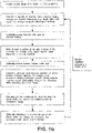
- Figure 1A provides a schematic cross section view diagram illustrating exemplary methods of the present disclosure for making printable semiconductor elements comprising printable semiconductor ribbons of single crystalline silicon from a bulk silicon wafer having a (111) orientation.
- Figure 1B provides a flow diagram setting forth processing steps, including repeatable processing steps, in the present methods for generating printable semiconductor elements from bulk silicon wafers.
- a silicon wafer having a (111) orientation 100 is provided.
- Silicon wafer 100 having a (111) orientation may be a bulk silicon wafer.
- a plurality of channels 110 having preselected physical dimensions, spacing and spatial orientations is etched into external surface 120 of silicon wafer 100, for example using a combination near field photolithography, lift-off and dry etching techniques.
- the spacing 130 between channels defines the width of the printable semiconductor ribbons fabricate using this method.
- a thermal oxide layer 140 is grown on channels 110 and external surface 120, for example by heating the (111) silicon wafer 100.
- a mask 150 is deposited on the side surfaces of channels 110 and external surface 120, for example using angled electron beam evaporation of one or more mask materials such as a metal or combination of metals, thereby generating masked and unmasked regions the silicon wafer 100.
- This masking step generates masked regions 160 of the side surfaces and unmasked regions 170 of the side surfaces of channels 110.
- the present disclosure includes aspects of the present disclosure wherein the entire side surfaces of channels 110 along depth 135 are masked (See e.g., Fig. 1D ).
- the extent that masked region extend down the side surfaces is controlled by angle of evaporation of mask materials, the "shadows" cast by the surface features on external surface 120 of wafer 100 and the degree of collimation of the flux of mask materials .
- the depth 135 of the trenches 110 and the extent of masked regions 160 of the side surfaces define the thickness of the printable semiconductor ribbon generated by these methods.
- exposed regions of thermal oxide layer 140 is removed prior to additional processing, for example using dry chemical etching techniques.
- unmasked regions 170 of the side surfaces of channels 110 are etched.
- unmasked regions 170 of the side surfaces of channels 110 are anisotropically etched such that etching between channels occurs preferentially along ⁇ 110> directions of the silicon wafer 100, thereby undercutting regions of (111) silicon wafer 100 between adjacent channels 110.
- the direction of the etch front ⁇ 110> directions is schematically shown by the dashed arrows in panel 3 of Figure 1B .
- an anisotropic etching system is chosen so that etching does not substantially occur along ⁇ 111> directions of the silicon wafer 100.
- anisotropic etching system The selectivity of the anisotropic etching system and the (111) orientation of silicon wafer 100 provides an intrinsic etch stop that is schematically represented as dotted line 175.
- Useful anisotropic etching systems for this aspect of the present disclosure include a wet chemical etching system using a hot basic solution.
- an etching system is chosen for this processing step that generates a printable semiconductor ribbon having a relatively smooth underside (e.g. roughness less than 1 nanometer).
- etching between channels generates printable semiconductor ribbons 200 that are entire undercut from the silicon wafer 100.
- the physical dimensions, shapes and spatial orientations of channels 110 are selected such that the etching processing steps generates printable semiconductor ribbons 200 that are connected at one or more ends to the silicon wafer 100.
- Printable semiconductor ribbons 200 generated by the present methods may be flat, thin and mechanically flexible.
- the mask 150 is removed, for example via wet chemical etching techniques.
- the present method includes the step of releasing printable semiconductor elements from the silicon wafer, for example by contact with an elastomeric stamp.
- contacting the printable semiconductor elements with an elastomeric stamp fractures one or more bridge elements connecting the printable semiconductor elements to the silicon wafer 100, thereby resulting in registered transfer of the printable semiconductor element(s) from silicon wafer 100 to the elastomeric stamp.
- Methods of the present disclosure include use of kinetically controlled peel rates to facilitate register transfer from silicon wafer 100 to an elastomeric stamp transfer device.
- the present disclosure includes high yield fabrication methods, further comprising the step of refinishing the external surface of the silicon wafer, for example by surface processing steps (e.g., polishing, grinding, etching, micromachining etc.) that generate a flat and/or smooth external surface of silicon wafer 100.
- surface processing steps e.g., polishing, grinding, etching, micromachining etc.
- refinishing silicon wafer 100 enables the fabrication process to be repeated multiple times, thereby providing high yields of printable semiconductor ribbons from a single silicon wafer starting material.
- Figure 1C provides a cross sectional view schematic processing diagram illustrating fabrication methods wherein the side surfaces of recessed features are partially, but not completely, masked.
- Figure 1D provides a cross sectional view schematic processing diagram illustrating fabrication methods wherein the side surfaces of recessed features are completely masked. As shown in Figure 1D , a portion, but not all, of the floors of the recessed features are also masked.
- the method includes the processing step of etching material underneath the masked side surfaces of the recessed feature.
- the partially masked floor configuration provides an inlet for etchant such that etching may occur between recessed features, such as adjacent recessed features.
- Methods of the present disclosure employing complete masking of the side surfaces of recessed feature are beneficial for providing enhanced accuracy and precision in the definition and selection of the thickness of the printable semiconductor elements.
- the side surfaces are completely masked such that the boundary of the passivation happens on the floors of the recessed features.
- the thickness of the ribbon is not defined by the boundary of the passivation, but instead by the height floor the floor of the trenches and the top surface of the wafer.
- the methods of fabricating printable semiconductor elements of the present disclosure may further comprise the step of refining the geometry, physical dimensions and morphology of the recessed features. Refining of the recessed features may be carried out at any point in the fabrication process after generation of the recessed features and prior to formation and/or release of the printable semiconductor elements. In a useful aspect of the present disclosure, refining of the recessed features is carried out prior to processing steps involving masking, partially or completely, the side surfaces of the recessed features.
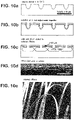
- Figure 1E provides an image of recessed features in Si (111) having a trench configuration generated without side surface refining. The recessed features shown in Figure 1E were defined by phase shift photolithography, metal lift-off and reactive ion etching, and subsequent removal of metal etch mask.
- Figure 1F provides an image of recessed features in Si (111) having a trench configuration generated with side surface refining.
- the recessed features shown in Figure 1F were defined by phase shift photolithography, metal lift-off and reactive ion etching, refining by anisotropic etching in hot KOH solution, and subsequent removal of metal etch mask. This sample is also treated by angled metal evaporation. As shown by a comparison of these figures, the floors and side surfaces of the trenches in Figure 1F are more smoothly defined than the floors and side surfaces of the trenches in Figure 1E .
- Refining in this context refers to material removal processing of surfaces of the recessed feature, such as the side surfaces and floors of recessed features. Refining includes processing resulting in smoother recessed feature surfaces and/or processing resulting in recessed features having more uniform physical dimensions and surface morphologies.
- the geometry, physical dimensions and/or morphology is refined via anisotropic etching techniques, for example etching using hot KOH solution.
- Anisotropic wet etch refining of trenches is particularly useful for generation of (111) silicon ribbons capable of register transfer.
- the advantages of the refining processing steps include: (i) providing improved definition of the trench floors determined from the crystallographic axes of the mother wafer, and (2) providing improved definition of the side surfaces of the trench by the crystallographic axes of the mother wafer.
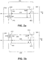
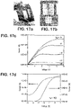
- Figures 2A and 2B provide schematic top plan view diagrams of printable semiconductor structures of the present disclosure comprising a printable semiconductor element and two bridge elements.
- Bridge elements are positioned distal to each other in the structure shown in Figure 2A and bridge elements are positioned proximal to each other in the structure shown in Figure 2B .
- printable semiconductor structures 290 comprise printable semiconductor element 300 and bridge elements 310.
- Bridge elements 310 are alignment maintenance elements that connect, optionally integrally connect, semiconductor element 300 to mother wafer 320.
- printable semiconductor element 300 and bridge elements 310 are partially or entirely undercut from mother wafer 320.
- printable semiconductor element 300, bridge elements 310 and mother wafer 320 are a unitary structure, such as a single, continuous semiconductor structure.
- Printable semiconductor elements 300 longitudinal extend length 330 along longitudinal axis 340 and extend width 350. Length 330 terminates in first and second ends 400 that are connected to bridge elements 310. Bridge elements 310 extend lengths 360 and extend widths 370. In the aspect of the present disclosure shown in Figures 1A and 1B , bridge elements connect to less than the entire width and/or cross sectional area of the ends 400 of printable semiconductor elements 300. As shown in Figures 2A and 2B , width 370 of bridge elements 310 is smaller than width 350 of printable semiconductor elements 300 to facilitate registered transfer. In addition, semiconductor elements 300 have surface areas of exposed external surfaces that are larger than the surface areas of exposed external surfaces of bridge elements 310. For some processing and transfer methods of the present disclosure, these dimensional attributes of bridge elements 310 and printable semiconductor elements 300 facilitate high precision registered transfer, assembly and/or integration of printable semiconductor elements 300
- bridge elements 310 holds semiconductor element 300 in a preselected spatial orientation before and/or during transfer from wafer 320, for example using an elastomeric stamp transfer device.
- the anchoring functionality of bridge elements 310 is desirable in many fabrication applications wherein the relative position, spacing and spatial orientation of one or printable semiconductor elements corresponds to a desired functional device and/or circuit design.
- the physical dimensions, spatial orientation and geometry of bridge elements is selected such that semiconductor elements 300 are capable of release upon contact with a transfer device. In some aspects of the present disclosure release is achieved by fracture, for example along the dotted lines shown in Figures 2B and 2B . It is important for some applications that the force required to fracture the bridge elements 310 is low enough so that the positions and spatial orientations of semiconductor elements 300 are not substantially disrupted during transfer.
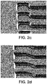
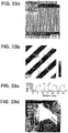
- FIGs 2C and 2D provide images of bridge elements connecting a printable semiconductor element to a mother wafer.
- Printable silicon elements and (narrow) bridge elements connecting printable elements to the mother (SOI) wafer are shown in Figure 2C .
- the geometry of the printable semiconductor element and bridge element is defined by SF6 etching.
- the printable semiconductor element and bridge element confirmation has rounded corners. The roundness of these corners and the overall geometry of these elements decrease the ability to release the printable semiconductor element with a PDMS transfer device.
- Printable silicon elements and (narrow) bridge elements connecting printable elements to the mother (SOI) wafer are also shown in Figure 2D .
- Geometry was defined by hot KOH anisotropic etching. As shown in Figure 2D , the printable semiconductor element and bridge element confirmation has sharp corners. The sharpness of those corners concentrates the stress at well defined breaking points and, thus, enhance the ability to release these elements be with a PDMS transfer device.
- EXAMPLE 1 Printed Arrays of Aligned GaAs Wires for Flexible Transistors, Diodes, and Circuits on Plastic Substrates
- Aligned arrays of GaAs wires with integrated ohmic contacts generated from high-quality, single-crystalline wafers by the use of photolithography and anisotropic chemical etching provide a promising class of material for transistors, Schottky diodes, logic gates and even more complex circuits on flexible plastic substrates. These devices exhibit excellent electronic and mechanical characteristics, which are both important to the emerging area of low cost, large area flexible electronics, often referred to as macroelectronics.
- Micron and nanoscale wires, ribbons, platelets, etc. of single crystal inorganic semiconductors are attractive building blocks for functional devices (e.g., optics, optoelectronics, electronics, sensing, etc.) that can be used in many applications.
- Si nanowires synthesized by "bottom-up" approaches can be assembled using Langmuir/Blodgett techniques (or microfluidics) into aligned arrays and used as transport channels for flexible thin-film transistors (TFTs) on plastic substrates.
- micro/nanoscale elements of Si in the form of ribbons with thicknesses of ⁇ 100 nm and widths ranging from several microns to hundreds of microns, can be generated from high-quality, single-crystalline bulk sources (e.g., silicon-on-insulator, SOI wafers, or bulk wafers) though "top-down" approaches.
- This type of material can be used to fabricate flexible TFTs on plastic with device mobilities as high as 300 cm 2 ⁇ V -1 ⁇ s -1 .
- the high quality of the wafer based source material leads to a silicon based semiconductor material with similarly good properties, which are beneficial for reliable, high performance device operation.
- the "top-down" fabrication process is attractive also because it offers the possibility of preserving the highly ordered organization nano/microstructures defined at the wafer level, during "dry transfer printing" to the final (e.g. plastic, or other) device substrate.
- high performance is possible with Si, even better characteristics (e.g. operating speed) is achieved with GaAs, for example, due to its high intrinsic electron mobility of ⁇ 8500 cm 2 ⁇ V -1 . s -1 .
- This example demonstrates the ability to build, with transfer printing as the assembly/integration strategy, various elemental units of functional circuits, such as inverters and logic gates, on plastic substrates using these types of MESFETs as well as GaAs wire based diodes as active components.
- functional circuits such as inverters and logic gates
- MESFETs as well as GaAs wire based diodes as active components.
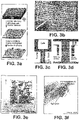
- Fig. 3A depicts the major steps for fabricating GaAs transistors, diodes and logic gates on plastic.
- the basic approach relies on "top-down" fabrication techniques to generate micro/nanowires with high purity and well-known doping profiles from bulk single crystal GaAs wafers.
- Ohmic contacts, formed on the wafer before fabricating the wires consist of 120 nm AuGe/20 nm Ni/120 nm Au deposited and annealed (450 °C for 1 min in a quartz tube with flowing N 2 ) on an epitaxial layer of 150-nm n-GaAs on a (100) semi-insulating GaAs (SI-GaAs) substrate.
- the contact stripes lie along the (0 ) crystallographic orientation, and have widths of 2 ⁇ m. In the case of transistors, the gaps between the ohmic stripes define the channel lengths.
- Photolithography and anisotropic chemical etching generates arrays of GaAs wires with triangular cross sections (inset of Fig. 3B ) and widths of ⁇ 2 ⁇ m, with ends that connect to the wafer ( Fig. 3B ). These connections act as 'anchors' to maintain the well defined orientation and spatial location of the wires, as defined by the layout of etch mask (i.e., photoresist pattern).
- Removing the etching mask and depositing a bilayer of Ti(2 nm)/SiO 2 (50 nm) via electron-beam evaporation prepares the surfaces of the wires for transfer printing.
- the triangular cross section ensures that the Ti/SiO 2 films on the surfaces of wires do not connect to those on the mother wafer, thus facilitating the yield of transfer printing.
- Laminating a slightly oxidized poly(dimethylsiloxane) (PDMS) stamp on the surface of the wafer leads to chemical bonding between the surface of the PDMS stamp and the fresh SiO 2 film by a condensation reaction. See top frame of Fig. 3A .
- Peeling back the PDMS stamp pulls the wires off of the wafer and leaves them bound to the stamp.
- Contacting this 'inked' stamp to a poly(ethylene terephthalate) (PET) sheet coated with a thin layer of liquid polyurethane (PU), curing the PU, peeling off the stamp and then removing the Ti/SiO 2 layer in 1:10 HF solution leaves ordered arrays of GaAs wires on the PU/PET substrate, as illustrated in the middle frame of Fig. 3A .
- the Ti/SiO 2 film not only serves as an adhesive layer to bond the GaAs wires to the PDMS but it also protects the surface of GaAs wires from possible contamination (e.g., by solvents and PU) during the processing.
- the pristine, bare surfaces of the wires and ohmic stripes are exposed for further lithographic processing and metallization to define source and drain electrodes (250 nm Au) that connect the ohmic contacts integrated on the wires.
- source and drain electrodes 250 nm Au
- these electrodes define the source and drain; for the diodes, they represent the ohmic electrode.
- Contacts 150 nm Ti/150 nm Au
- the width of the gate electrode represents the critical dimension for controlling the operation speed.
- the position of this electrode between the source and drain is relatively unimportant in this work.
- This tolerance to poor registration which is not present in non-self aligned high speed MOSFET (metal-oxide-semiconductor field-effect transistor) type devices, is critically important for reliably achieving high speed operation on plastic substrates where precise registration is often challenging or impossible due to slight uncontrolled deformations that can occur in the plastic during processing.
- Connecting multiple transistors and diodes together in appropriate geometries generates functional logic circuits.
- the scheme of Fig. 3A shows a NOR gate.
- a scanning electron microscope (SEM) image shows ten parallel wires that form the semiconductor component of a transistor.
- the channel length and the gate length of this device are 50 and 5 ⁇ m, respectively. These geometries are used for building the simple integrated circuits, i.e., logic gates.
- the Ti/Au stripe in the gap between the source and drain electrodes forms a Schottky contact with the n-GaAs surface. This electrode acts as a gate for modulating the flow of current between source and drain.
- Diodes ( Fig. 3D ) use wires with ohmic stripes on one end and Schottky contacts on the other.
- Fig. 3E and 3F show images of a collection of GaAs transistors, diodes and simple circuits on a PET substrate. In Fig. 3F the PET sheet with circuits is bent around the shaft of a white marker, indicating the flexibility of these electronic units.
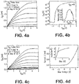
- the DC characteristics of the wire based MESFETs on plastic exhibit qualitatively the same behavior ( Fig. 4A ) as those formed on the wafer.
- the flow of current between source and drain ( I DS ) is well modulated by the bias applied to the gate (V GS ), i.e., the I DS decreases with decrease of V GS .
- the negative V GS depletes the effective carriers (i.e., electrons for n-GaAs) in the channel region and decreases the channel thickness.
- the depletion layer equals to the thickness of n-GaAs layer and the flow of current between source and drain is pinched off (i.e., the / DS becomes essentially zero).
- the I DS drops to almost zero at the V GS less than -2.5 V.
- the pinch-off voltage i.e. gate voltage V GS
- V DS drain-source voltage
- V DS saturation region
- the transfer curve of this transistor is shown in Fig. 4B .
- the ON/OFF current ratio and maximum transconductance are determined from Fig.
- the overall source-drain current is a function of the number of wires (i.e., the effective channel width) and the distance between source and drain (i.e., the channel length).
- transistors with short channels can provide relatively high currents.
- the ON/OFF current ratio tends to decrease because of the difficulty to completely pinch off the current.
- the I DS of transistor with channel length of 25 ⁇ m is still on the order of several microamperes even for V GS of -5 V.
- the GaAs-wire Sckottky diodes on plastic exhibit the typical behavior ( Fig. 4D ) of rectifiers, i.e., the forward current (/) increases quickly with increasing forward bias voltage (V) while the reverse current remains small even at reverse biases as large as 5 V.
- ⁇ B and n are commonly used as the evaluation criteria of Schottky interfacial properties. Both are highly dependent on the interface charge states between metal and GaAs, i.e., an increase of charge states will cause the decrease of ⁇ B and the increase of n value.
- ⁇ B and n are determined from the inset of Fig, 4D to be 512 meV and 1.21, respectively. These devices have a somewhat lower Schottky barrier (512 meV versus ⁇ 800 meV) and larger ideality factor (1.21 versus ⁇ 1.10) compared with the diodes built on wafers.
- GaAs-wire devices i.e., MESFETs and diodes
- MESFETs and diodes can be integrated into logic gates for complex circuits.
- connecting two MESFETs with different channel lengths, which have different saturation currents forms an inverter (logic NOT gate) ( Fig. 5A and 5B ).
- the load (top) and switching transistor (bottom) have channel lengths of 100 and 50 ⁇ m, respectively, and channel widths of 150 ⁇ m and gate lengths of 5 ⁇ m.
- the inverter is measured in the saturated region, i.e., the V dd is biased with 5 V.
- a large negative voltage (logic 0) is applied to the gate of the switching transistor ( V in ) to turn it off
- the voltage of the output node ( V out ) equals the V dd (logic 1, high positive voltage) because the load transistor is always on.
- An increase in V in turns the switching transistor on and provides a large current through both the switching transistor and the load transistor.
- the V out decreases to a low positive voltage (logic 0) when the switching transistor is completely turned on, i.e., the V in is a large positive voltage (logic 1).
- Fig. 5C shows the transfer curve.
- the logic status of V out is shifted to voltages suitable for further circuit integration by adding a level-shifting branch composed of Schottky diodes (as shown in Fig. 3D ).
- GaAs wires with integrated ohmic contacts fabricated using "top-down" procedures with high-quality, bulk single-crystal wafers provide a high performance 'printable' semiconductor material and a relatively easy path to transistors, diodes and integrated logic gates on flexible plastic substrates.
- the separation of hightemperature processing steps (e.g. formation of ohmic contacts) from the plastic substrates and the use of PDMS stamps for transfer printing well ordered arrays of GaAs wires are key features of the approach described herein.
- GaAs wires as the semiconductor is attractive for large area printed electronics with demanding requirements on operating speed because (i) GaAs has a high intrinsic electron mobility ( ⁇ 8500 cm 2 V -1 s -1 ) and has established applications in conventional high frequency circuits, (ii) MESFETs built with GaAs offer simpler processing than MOSFETs because the MESFETs do not require gate dielectrics, (iii) GaAs MESFETs do not suffer from parasitic overlap capacitances that occur in non-self aligned MOSFETs, (iv) high-speed operation in GaAs MESFETs is possible even with the modest levels of patterning registration and resolution that can be achieved easily on large area plastic substrates.
- the GaAs wafer (IQE Inc., Bethlehem, PA) has an epitaxial Si-doped n-type GaAs layer (with carrier concentration of 4.0 ⁇ 10 17 cm -3 ) grown on a (100) semi-insulating GaAs wafer through molecular beam epitaxial (MBE) deposition in a high vacuum chamber.
- MBE molecular beam epitaxial
- the lithography processes employ AZ photoresist (AZ 5214 and AZ nLOF 2020 for positive and negative imaging, respectively), which are carried out at temperatures ( ⁇ 110 °C) compatible with the plastic substrates, i.e., poly(ethylene terephthalate) (PET of ⁇ 175 ⁇ m in thickness, Mylar film, Southwall Technologies, Palo Alto, CA) sheets covered with a thin layer of cured polyurethane (PU, NEA 121, Norland Products Inc., Cranbury, NJ).
- PET poly(ethylene terephthalate)
- the GaAs wafers with photoresist mask patterns are anisotropically etched in the etchant (4 mL H 3 PO 4 (85 wt%), 52 mL H 2 O 2 (30 wt%), and 48 mL deionized water) that was cooled in the ice-water bath. All the metals are evaporated at a speed of ⁇ 4 ⁇ /s by an electron-beam evaporator (Temescal). The evaporation os stopped to cool the samples (for 5 min) to prevent the plastic substrates from melting when 50 nm thick metals are deposited. After the samples are cooled, repeating the evaporation/cooling cycle deposited more metals.
- the etchant 4 mL H 3 PO 4 (85 wt%), 52 mL H 2 O 2 (30 wt%), and 48 mL deionized water
- GaAs wires with ohmic contacts formed from bulk wafers, soft lithographic transfer printing techniques, and optimized device designs enable mechanically flexible transistors to be formed on low cost plastic substrates, with individual device speeds in the gigahertz range and with high degrees of mechanical bendability.
- the approaches disclosed herein incorporate materials in simple layouts that are fabricated with modest lithographic patterning resolution and registration. This example describes the electrical and mechanical characteristics of high-performance transistors. The results are important in certain applications, including, but not limited to, high-speed communications and computations, and the emerging classes of large area electronic systems ("macroelectronics").
- TFTs Flexible thin film transistors
- inorganic materials such as amorphous/polycrystalline oxides and chalcogenides, polysilicon as well as single crystalline silicon nanowires and microstructured ribbons, exhibit much higher mobilities (10 ⁇ 300 cm 2 ⁇ V -1 ⁇ S -1 ) than those of polycrystalline organic thin films ( ⁇ 1 cm 2 ⁇ V -1 ⁇ s -1 in general).
- wire arrays of single crystalline GaAs which have very high intrinsic electron mobility ( ⁇ 8500 cm 2 ⁇ v -1 ⁇ s -1 ), can serve as transport channels for TFTs in the geometry of metal-semiconductor field-effect transistors (MESFETs).
- MSFETs metal-semiconductor field-effect transistors
- This example shows that with optimized designs, similar devices can operate with frequencies in the GHz regime, even with modest lithographic resolution, and with good bendability.
- experimental results show that GaAs wire-based MESFETs on plastic substrates exhibit cutoff frequency higher than 1.5 GHz for transistors with gate length of 2 ⁇ m, with modest changes in the electrical properties for bend radii down to ⁇ 1 cm when ⁇ 200 mm thick substrates are used. Simple simulations of device behavior agree well with the experimental observations, and operating frequencies in the S-band (5 GHz) are achievable.
- GaAs wire ( ⁇ 2 ⁇ m in width) arrays with integrated ohmic stripes are fabricated from a (100) semi-insulating GaAs (SI-GaAs) wafer with epitaxial layer of 150-nm n-GaAs through photolithography and anisotropic chemical etching.
- a thin bilayer of Ti(2 nm)/SiO 2 (50 nm) is deposited on the undercut GaAs wires to serve as the adhesive layer to facilitate the transfer printing process as well as to protect the flat surfaces of wires and ohmic contacts from contamination by organics (primarily those that transfer from the surfaces of the stamps) involved in the process.
- This layer is removed by dipping the samples in 1:10 HF solution to expose the clean surfaces of GaAs wires for device fabrication in the sequential steps.
- the thin thickness (compared with the thickness of photoresist layers which are used as the adhesive layer for transfer printing in our previous work) of this Ti/SiO 2 layer results in a relatively flat surface of plastic poly(ethylene terephthalate) (PET) sheet, on which GaAs wire arrays are printed with the assistance of a spin cast thin layer of polyurethane (PU).
- PET plastic poly(ethylene terephthalate)
- PU spin cast thin layer of polyurethane
- Fig. 7A shows the current flow between source and drain ( I DS ) as a function of gate voltage ( V GS ) (inset) and as a function of source/drain voltage at different V GS , for a device with gate length of 2 ⁇ m.
- the pinch-off voltage at V DS of 0.1 V i.e., linear region
- the ON/OFF current ratio determined from averaged measurements on many devices, is ⁇ 10 6 .
- the devices exhibit negligible hysteresis (inset), which is particularly important for high-speed response.
- the devices show good device-to-device uniformity; Table 1 lists the statistical results (with device number >50) of MESFETs with channel lengths of 50 pm and different gate lengths.
- the DC characteristics are almost independent of the gate length except that devices with larger gate lengths exhibit somewhat lower ON/OFF ratios.
- the gate length plays a critical role, however, in determining the operating frequencies as described in the following.
- Fig. 8A shows the layout of a device designed for microwave testing.
- Each unit of the test structure contains two identical MESFETs with gate lengths of 2 ⁇ m and channel lengths of 50 ⁇ m with a common gate, and probing pads configured to match the layout of the RF probes.
- the drain (D) terminal is held at 4 V (versus source (S)) and the gate (G) is driven by a bias of 0.5 V coupled with a RF power of 0 dBm, which has an equivalently voltage amplitude of 224 mV with 50 ⁇ .
- the measurement is carried out using HP8510C Network Analyzer calibrated from 50 MHz to 1 GHz using a standard SOLT (Short-Open-Load-Through) technique on a CascadeMicrotech 101-190B ISS substrate (a piece of ceramic chip covered with laser trimmed gold patterns) through WinCal 3.2 for error corrections.
- SOLT Short-Open-Load-Through
- CascadeMicrotech 101-190B ISS substrate a piece of ceramic chip covered with laser trimmed gold patterns
- WinCal 3.2 for error corrections.
- short calibration is thought to be perfect short and open calibration is thought be perfect open.
- the reference plane of measurement is set between the input probe and the output probe. In other words, parasitic components of contact pads are included in the measurement.
- the small-signal current gain ( h 21 ) can be extracted from the measured S-parameters of the device. This quantity exhibits a logarithmic dependence on the frequency of input RF signal ( Fig. 9A ).
- the transconductance (g m ), the output resistance (R DS ), and the charging resistance (R ⁇ , which accounts for the fact that the charge on the channel cannot instantaneously respond to changes in V Ds ) are extracted from DC measurements.
- the intrinsic capacitances associated with the MESFET include contributions from the depletion layer, edge fringing and geometric fringing capacitances. Each of these are computed using standard equations for conventional devices with channel widths equal to the summed widths of the individual GaAs wires.
- 150 ⁇ m and 200 ⁇ m are the width and length of either source or drain pad.
- C GS capacitance between the gate and the source, include all three kinds of capacitance; while C DS and C DG only contain the edge fringing capacitance and the geometric fringing capacitance. The contributions of C edge and C geometric might be ignored without a significant effect on the simulation results, in most cases, because they are much smaller than C depletion , which is appropriate to the gate length.
- This model accounts for the behavior of the wire array devices on plastic, including the variation in f T with gate length.
- Fig. 8C compares the measured (symbols) and calculated (dashed line) f T of GaA-wire MESFETs with different gate lengths and channel length of 50 ⁇ m. This modeling suggests that f T can be increased significantly by reducing the gate length or by further optimizing the design of the layers in the GaAs mother wafers.
- the current recovers when the substrate is released after bending in either direction, suggesting that deformations of the plastic substrate and the other components of the devices are elastic in this regime.
- Fig. 9C gives the dependence of the measured ON/OFF current ratio in the saturation region on strain, showing qualitative agreement with the discussion above.
- the results of this example show that the bending induced surface strain (in both tension and compression, as high as 0.71%) does not significantly degrade the performance of the MESFETs fabricated from the modified procedure. More importantly, releasing the sample in its bent state returns the device performance to its original state.
- This example introduces a type of thin film transistor that uses aligned arrays of thin (sub-micron) ribbons of single crystal silicon created by lithographic patterning and anisotropic etching of bulk silicon (111) wafers.
- Devices that incorporate such ribbons printed onto thin plastic substrates show good electrical properties and mechanical flexibility. Effective device mobilities, as evaluated in the linear regime, are as high as 360 cm 2 V -1 s -1 , and on/off ratios are > 10 3 .
- High-performance flexible electronic devices e.g. transistors, simple circuit elements, etc.
- micro/nanowires ribbons or tubes that are cast, painted, or printed onto plastic substrates.
- Thin, high aspect ratio materials structures allow bendability, and, in certain structural forms, stretchability, in single-crystalline semiconductors of materials that are inherently fragile and brittle in bulk.
- these types of semiconductors offer interesting alternatives to vacuum and solution processable poly/noncrystalline organic materials, which usually display significantly lower performance in terms of carrier mobility.
- TFT thin film transistor
- 111 low-cost bulk Si
- Fig. 10 illustrates a top-down method that generates thin ( ⁇ 1 ⁇ m) ribbons from the surface of a Si (111) wafer (Montco, Inc., n-type, 0.8-1.8 ⁇ .cm).
- the process begins with near-field phase shift photolithography 13 followed by metal lift-off and SF 6 plasma etching (Plasmatherm RIE system, 40 sccm SF 6 , 30 mTorr, 200 W RF power for 45 sec.) to produce an array of ⁇ 1 ⁇ m deep, 1 ⁇ m wide trenches in the Si surface ( Figure 1 (a) ).
- the spacing between the trenches defines the width of the ribbons (generally 10 ⁇ m).
- thermal oxide is grown on the wafer at 1100°C.
- Two metal deposition steps performed by angled electron beam evaporation of Ti/Au (3/30 nm), provide partial coverage of the trench side surfaces ( Fig. 10B ).
- the 'shadows' cast during these angled evaporations define the thicknesses of the ribbons.
- the conditions of the trenching etch, the angle of evaporation and the degree of collimation of the flux of metal control the extent of this shadowing and, therefore, the ribbon thickness.
- a CF 4 plasma etch (40 sccm CF 4 , 2 sccm O 2 , 50 mTorr base pressure, 150 W RF power for 5 min) removes exposed oxide.
- a hot KOH solution (3:1:1 H 2 O:KOH:IPA by mass, 100 °C) undercuts the ribbons.
- the etch front advances in the ⁇ 110> directions while preserving the (111) planes ( Fig. 10C ) and produces free-standing ribbons that cover a large portion (75-90%) of the original wafer.
- the etch mask is designed to leave each of the ribbons anchored to the wafer at the ends of the trenches ( Fig. 12A and 12B ). Removing this mask with Kl/I 2 (2.67/0.67 wt%) in water followed by HF completes the fabrication. Ribbons generated in this manner are thin, flat, and mechanically flexible ( Fig.
- FIG. 10E Similar to those produced using previously described approaches with expensive silicon-on-insulator wafers .
- Fig. 11A Atomic force microscopy shows that the thickness ranges from ⁇ 115 to ⁇ 130 nm across a typical ribbon. These variations show up as slight color variations in optical micrographs ( Fig. 12E ).
- the roughness as measured by AFM of a 5 x 5 ⁇ m region of the underside of one of these ribbons, displayed in Fig. 12B is 0.5 nm. This value is larger than the top polished surface (0.12 nm) or the underside of a ribbon generated from and SOI wafer (0.18 nm) measured by the same methods.
- the ribbons can be transferred to another (flexible) substrate via a high (>95%) yield printing process, as outlined in Fig. 12 .
- a PDMS stamp is laminated against the wafer and then peeled back quickly to retrieve the ribbons. This type of process relies on kinetic control of adhesion to the stamp.
- the stamp thus "inked,” ( Fig. 12B and 12E ) can print the ribbons by contact to another substrate.
- Ribbons printed onto an ITO-coated 0.2 mm thick PET substrate can be used to make high performance flexible bottom-gate TFTs on plastic with ITO as the gate electrode.
- a layer of SU-8 deposited onto the ITO gate prior to printing serves as a gate dielectric and a glue to facilitate ribbon transfer.
- the ribbons sink into uncured SU-8 such that their tops are flush with the surface of the glue, leaving about 2 ⁇ m of dielectric between the ribbons' bottom surfaces and the ITO.
- Thick ( ⁇ 0.2 ⁇ m) Ti source and drain contacts defined by photolithography (100 ⁇ m length x 100 ⁇ m width) and wet etching with HF/H 2 O 2 form Schottky barrier contacts for the source and drain electrodes.
- These bottom-gate devices display characteristic n-type enhancement mode MOSFET gate-modulation.
- the mobility of the ribbons themselves should be about 20% higher than the device level mobility (440 cm 2 V -1 s -1 linear and 120 cm 2 V -1 s -1 saturation), since they fill only about 83% of the channel due to the spaces between them.
- the ribbon devices survive when the substrate is bent to modest (15 mm) radii but degrade seriously at sharper (5 mm) bends for the 0.2 mm thick substrates.
- this example demonstrates a high-yield fabrication strategy for producing printable single-crystal silicon ribbons from a bulk silicon (111) wafer. Refinishing the bulk wafer's surface after fabrication permit multiple repetitions, producing tens or even hundreds of square feet of ribbons from one square foot of starting material. TFTs made from these ribbons on plastic demonstrate their use as high-performance flexible semiconductors. These devices and the strategies to fabricate them are useful not only for large area flexible electronics, but also for applications that require three dimensional or heterogeneous integration or other features that are difficult to achieve using conventional silicon microfabrication approaches.
- ⁇ s-Sc microstructured semiconductors
- single crystalline ⁇ s-GaN is of great interest, as it has superior material properties that include a wide band gap (3.4 eV vs 1.4 eV of GaAs) leading to high breakdown field (3 MV cm -1 vs 0.4 MV cm -1 of GaAs), high saturation carrier velocity (2.5 * 10 7 cm S -1 vs 10 7 cm S -1 of GaAs), and good thermal conductivity (1.3 W cm -1 vs 0.5 W cm -1 of GaAs).
- the heterogeneous integration in the form of AlGaN/GaN heterostructures yields device grade materials with a high conduction band offset and piezoelectric responsiveness with sheet carrier densities lying in the 1.0 x 10 13 cm -2 range.
- These attractive properties made GaN suitable for requiring both high frequency and high power performance, such as electronic devices for wireless communication, full color light emitting devices, and UV photodetectors for optoelectronic systems.
- Fig. 15 schematically illustrates the steps used in the fabrication of the HEMT devices.
- the process starts with the formation of an ohmic contact (Ti/Al/Mo/Au) on the bulk GaN heterostructure wafer using a standard sequence photolithographic and lift-off steps ( Fig. 15A ).
- a PECVD oxide layer and Cr metal are then deposited to serve as a mask for subsequent dry etching.
- Photolithography and etching of the Cr and PECVD oxide define the geometries desired for GaN ribbons that serve as the solid ink for subsequent printing ( Fig. 15B ).
- ICP dry etching is used to remove the exposed GaN ( Fig. 15C ).
- the Cr layer is removed by this ICP etching step, but left the thicker PECVD oxide layer essentially intact on top of the GaN.
- Anisotropic wet etching with tetramethyl ammonium hydroxide (TMAH) ( Fig. 15D ) removes the underlying Si and detaches the GaN ribbons from the mother substrate.
- TMAH tetramethyl ammonium hydroxide
- the PECVD oxide serves to protect the ohmic contacts from degradation.
- the remaining PECVD oxide which has been severely roughened by the plasma and wet etching steps, is then removed using a BOE (buffered oxide etchant) process step.
- a new smooth, sacrificial silicon oxide layer is deposited subsequently on the top of GaN ribbons by e-beam evaporation.
- a print to GaN ribbons the wafer was contacted with a poly-dimethylsiloxane (PDMS) slab ( Fig. 15E ), and on fast removal from the mother substrate, a complete transfer of the ⁇ s-GaN to the PDMS is obtained.
- This "inked" slab is then laminated with a poly(ethyleneterepthalate) sheet (PET) coated with polyurethane (PU) ( Fig. 15F ) and, from the topside, a UV light is used to cure the PU ( Fig. 15H ).
- PET poly(ethyleneterepthalate) sheet
- PU polyurethane
- ⁇ s-Sc microstructured semiconductor
- the ⁇ s-GaN ribbon has two narrow bridges (i.e. two breaking points as indicated as arrows in Fig. 14C ) at the ends of the GaN ribbon to facilitate their registered transfer to the PDMS printing tool ( Fig. 15E ).
- This architecture represents a significant improvement over the 'peanut' design reported previously. The fracture that mediates the transfer process was found to be vastly efficient with this design.
- Fig. 16A and 16B show optical images of the GaN wafer taken before and after TMAH anisotropic etching step, respectively. The different colors of the freestanding and supported GaN microstructure are easily distinguishable in these images.
- Fig. 16C and 16D show scanning electron micrograph (SEM) images taken at intermediate stages of the TMAH etching step that cuts the underlying Si. The magnified image of Fig. 16D and dashed line area of Fig.
- FIG. 16B powerfully illustrate the highly anisotropic nature of this indicate that Si etching process, one propagated essentially only in a direction perpendicular to the orientation of the GaN ribbon.
- the preferential etching occurs along the (110) direction; the Si (111) surfaces, as noted in Fig. 14C , served as an innate etch blocking mask.
- Fig. 16E shows an SEM image of an inked PDMS slab where the ⁇ s-GaN was transferred with full tension of its on-wafer registration.
- the image of Fig. 16F shows an SEM micrograph of the printed structures where, the final step, the ⁇ s-GaN heterostructure devices are transferred to the PU coated PET substrate.
- Fig. 17A and 17B present representative optical images of ⁇ s-GaN based HEMTs after transfer to the PET substrate.
- the various contrast correspond to the various lends of the cross section schematic of these devices is shown in Fig. 14B .
- the active electron channel is formed between the two ohmic contacts (Ti/AI/Mo/Au) and the electron flow rate (or current) is controlled by the schottky (Ni/Au) gate contact.
- the channel length, the channel width, and the gate width of the devices shown in Fig. 17B are 20, 170, and 5 ⁇ m respectively.
- Fig. 17C shows typical drain current -voltage (I-V) characteristics of the plastic supported GaN HEMT devices; the gate was biased from -3 to 1 V in steps of 1 V. The device exhibits a maximum drain current of ⁇ 5 mA at a gate bias of 1 V and drain bias of 5 V.
- the device exhibits threshold voltage (V th ) of -2.7 V, an on/off ratio of 10 3 , and a transconductance of 1.5 mS.
- V th threshold voltage
- the transconductance of GaN HEMTs with the same device geometry but prior to transfer has a transconductance of 2.6 mS. The transfer process appears to lead to reduction in this value of about 38%.
- Fig. 18A shows a series of transfer curves measured as a function of bending radius (and its corresponding strain). For bending radii down to 1.1 cm (corresponding to strains of the order of 0.46 %), we observe very stable responses in the measured transconductance, threshold voltage, and on/off ratios.
- Fig. 18C shows a sequence of current-voltage (I-V) curves measured at both the positions of maximum strain and after its release.
- I-V current-voltage
- this example describes a process suitable for printing high performance GaN HEMTs in flexible forms on plastic substrates.
- Our results suggest that ⁇ s-GaN technology provide interesting opportunities for developing next generation macroelectronic devices, such as high performance mobile computing and high speed communication systems.
- GaN microstructures are fabricated on a heterostructure GaN on silicon (100) wafer (Nitronex) comprised of three layers of III-V semiconductor: AIGaN layer (18 nm, undoped); GaN buffer layer (0.6 ⁇ m, undoped); and AIN transition layer (0.6 ⁇ m).
- AIGaN layer (18 nm, undoped
- GaN buffer layer 0.6 ⁇ m, undoped
- AIN transition layer 0.6 ⁇ m.
- a Ti/Al/Mo/Au (15/60/35/50 nm from bottom to top) metal layer is then deposited.
- Electron-beam evaporation is used to deposit Ti, Al, and Mo, while Au was deposited by thermal evaporation.
- the contacts are defined using a lift-off process. The contacts are annealed at 850 °C for 30 sec in a rapid thermal annealing system using an N 2 ambient.
- the PECVD oxide (Plasmatherm, 400 nm, 900 mTorr, 350 sccm 2% SiH 4 /He, 795 sccm NO 2 , 250 °C) and Cr metal (E-beam evaporator, 150 nm) layers are deposited as the mask materials for subsequent ICP etching.
- Photolithography, wet etching (Cyantek Cr etchant) and RIE processing 50 mTorr, 40 sccm CF 4 , 100 W, 14 min) define the ribbon geometries of the GaN.
- ICP dry etching (3.2 mTorr, 15 sccm Cl 2 , 5 sccm Ar, -100V Bias, 14 min) is used to remove the exposed GaN, and the underlying Si is then etched away using a TMAH wet etching solution (Aldrich, 160 °C for 5 min).
- the sample is dipped in BOE (6:1, NH 4 F: HF) for 90 sec to remove the PECVD oxide and a new 50 nm e-beam evaporated SiO 2 layer deposited on top of the GaN ribbons.
- the GaN wafer is then contacted with a PDMS slab (Sylgard 184, Dow corning) which is then pealed away at peel rate > 0.01 m s -1 to pick up the ⁇ s-GaN elements.
- the PDMS slab inked with the ⁇ s-GaN is then laminated to a poly(ethyleneterepthalate) sheet (PET, 100 ⁇ m in thickness, Glafix Plastics) coated with polyurethane (PU, Norland optical adhesive, No. 73).
- PET poly(ethyleneterepthalate) sheet
- PU Norland optical adhesive, No. 73
- a negative photoresist (AZ nLOF2020) is used to pattern the Schottky contact area and a Ni/Au (80/100 nm) layer is then deposited by ebeam evaporation.
- the PR is removed using a lift off process in conjunction with an AZ stripper (KWIK for 5 hours).
- EXAMPLE 5 Printable Semiconductor Elements Derived from Bulk Wafer of GaAs with Multiple Epitaxial Layers.
- the present disclosure includes methods of making printable semiconductor ribbons using bulk wafers of GaAs as starting materials.
- the ribbons are generated from a high-quality bulk wafer of GaAs with multiple epitaxial layers.
- the wafer is prepared by growing a 200-nm thick AlAs layer on a (100) semi-insulating GaAs (SI-GaAs) wafer, followed by sequential deposition of a SI-GaAs layer with thickness of 150 nm and Si-doped n-type GaAs layer with thickness of 120 nm and carrier concentration of 4x10 17 cm -3 .
- a pattern of photoresist lines defined parallel to the (0 ) crystalline orientation serves as masks for chemical etching of the epilayers (including both GaAs and AlAs).
- Anisotropic etching with an aqueous etchant of H 3 PO 4 and H 2 O 2 isolated these top layers into individual bars with lengths and orientations defined by the photoresist, and with side surfaces that form acute angles relative to the wafer surface.
- Removing the photoresist after the anisotropic etching and then soaking the wafer in an ethanol solution of HF (2:1 in volume between ethanol and 49% aqueous HF) removes the AlAs layer and released ribbons of GaAs (n-GaAs/SI-GaAs).
- ethanol instead of water, for this step reduces cracking that can occur in the fragile ribbons due to the action of capillary forces during drying.
- the lower surface tension of ethanol compared to water also minimizes drying-induced disorder in the spatial layout of the GaAs ribbons.
- GaAs wafers with customer-designed epitaxial layers are purchased from IQE Inc., Bethlehem, PA.
- the lithographic processes employed AZ photoresist, i.e., AZ 5214 and AZ nLOF 2020 for positive and negative imaging, respectively.
- the GaAs wafers with photoresist mask patterns are anisotropically etched in the etchant (4 mL H 3 PO 4 (85 wt%), 52 mL H 2 O 2 (30 wt%), and 48 mL deionized water) that is cooled in the ice-water bath.
- the AlAs layers are dissolved with a diluted HF solution (Fisher ® Chemicals) in ethanol (1:2 in volume).
- the samples with released ribbons on mother wafers are dried in a fume hood.
- the dried samples are placed in the chamber of electron-beam evaporator (Temescal FC-1800) and coated with sequential layers of 2-nm Ti and 28-nm SiO 2 .
- EXAMPLE 6 Multi-layer Arrays Printable Semiconductor Elements Derived from Si (111) Wafers.
- the present disclosure also includes methods and compositions providing multilayer arrays printable semiconductor elements derived from Si(111) wafer precursor materials.
- Figure 19 provides a process flow schematic illustrating a method of the present disclosure for making multilayer arrays of printable semiconductor elements.
- a silicon wafer having a (111) orientation is provided.
- An external surface of the wafer is patterned with an etch resistant mask, thereby generating masked regions having dimensions selected to define the lengths and widths of printable semiconductor ribbon in the multilayer array.
- the etch resistant mask is a thermally grown SiO 2 layer.
- the silicon wafer is etched predominately in a directed orthogonal to the patterned external surface.
- the etching system employed generates recessed features having contoured side surfaces.
- the side surfaces of the recessed features have a selected, spatially varying contour profile having a plurality of contour features, such as side surfaces with a periodic scalloped contour profile and/or a contour profile having deep ridges present on the side surfaces of the recessed features.
- Exemplary means for generating recessed features having a selected contour profile include STS-ICPRIE and BOE etching systems providing cyclic exposure of the silicon wafer to reactive ion etchant gases and etch resist materials. As shown in panel 3 of figure 19 , this processing step generates a plurality of silicon structures having selectively contoured side surfaces positioned adjacent to the recessed features.
- the processed silicon wafer having recessed features and silicon structure is subject to deposition of an etch resistant mask materials such that the contoured side surfaces of the recessed features is only partially coated with deposition material.
- the selected contour profile of the side surfaces of the recessed features determines, at least in part, the spatial distribution of mask material on the side surfaces. This processing step, therefore, defines the thickness of printable semiconductor elements in the multi layer stack.
- the wafer may be exposed to angled vapor deposition of a metal or combination of metals resulting in deposition of material predominately on ridges present in the contoured surfaces of the recessed features and substantially no deposition on regions of the contoured surface that are in the "shadows" of the ridges present for example to recessed regions of the side walls.
- the "shadows" casts by features in the selected contour profile, such as ridges, ripples and scalloped shaped features, therefore, at least in part define the thickness of the printable semiconductor elements in the multilayer array.
- Use of gold deposition materials is beneficial due to its good adherence to the exposed silicon surface.
- the wafer is next subjected to anisotropic etching, for example via exposure to a basic solution such as KOH. Regions between the recessed features are etched such that etching occurs along ⁇ 110> directions of the silicon wafer, thereby fabricating a multilayer array of printable semiconductor elements each of which comprising a partially or entirely undercut silicon structures.
- the present disclosure includes methods wherein etching along ⁇ 110> directions of the silicon wafer proceeds to completion between adjacent recessed features, thereby entirely undercutting the printable semiconductor element(s).
- the etching system chosen in combination with the (111) orientation of the silicon wafer results in a faster etch rate along ⁇ 110> directions than along ⁇ 111> directions of the wafer.
- the position, shape and spatial orientation of recessed features are selected to form alignment maintenance elements, such as bridge elements connecting the printable semiconductor element to the wafer.
- alignment maintenance elements such as bridge elements connecting the printable semiconductor element to the wafer.
- bridge elements are provided that connect the ends of the semiconductor ribbons in the multilayer array to the silicon wafer.
- Panel 5 of figure 19 shows an optional processing step wherein the bridge elements are released from the silicon wafer, for example via washing, etching or other material removal processes, thereby generating a multilayer stack of printable semiconductor elements.
- printable semiconductor elements in the array can be released via contact printing methods.
- printable semiconductor elements in the multilayer array are sequentially released and transferred from the silicon wafer via repeatedly bringing the printable semiconductor elements in contact with a transfer device, such as an elastomeric stamp.
- Figure 20 provides SEM images of Si (111) in angled-view (a, c, e, g) and cross-sectional view (b, d, f, h): (a and b) after STS-ICPRIE and BOE etching, (c and d) after metal protection on the side surfaces, (e through h) after KOH etching for 2 min (e and f) and 5 min (g and h) followed by metal cleaning.
- Figure 21 provides (a) provides a photograph of a large-scale aligned array of four-layered Si (111) ribbons. (b and c) Top-view and (d and e) angled-view SEM images of the four-layered Si (111) shown in (a).
- Figure 22 provides (a) Photograph and (b and c) OM images of released flexible Si (111) ribbons. (d to f) SEM images of the ribbons shown in (a).
- Figure 23 provides (a) Optical images of aligned Si (111) ribbons transferred on PDMS substrate. (b) AFM image of four ribbons from the array shown in (a). Photograph of a flexible polyester film that houses four patterns of Si (111) arrays from four cycles of transferring from a single Si chip.
Landscapes
- Physics & Mathematics (AREA)
- General Physics & Mathematics (AREA)
- Junction Field-Effect Transistors (AREA)
- Thin Film Transistor (AREA)
- Manufacturing Of Printed Wiring (AREA)
- Metal-Oxide And Bipolar Metal-Oxide Semiconductor Integrated Circuits (AREA)
- Recrystallisation Techniques (AREA)
Priority Applications (1)
| Application Number | Priority Date | Filing Date | Title |
|---|---|---|---|
| EP22164385.1A EP4040474B1 (en) | 2005-06-02 | 2006-06-01 | PRINTABLE SEMICONDUCTOR STRUCTURES AND THEIR MANUFACTURING AND ASSEMBLY PROCESSES |
Applications Claiming Priority (5)
| Application Number | Priority Date | Filing Date | Title |
|---|---|---|---|
| US11/145,574 US7622367B1 (en) | 2004-06-04 | 2005-06-02 | Methods and devices for fabricating and assembling printable semiconductor elements |
| US11/145,542 US7557367B2 (en) | 2004-06-04 | 2005-06-02 | Stretchable semiconductor elements and stretchable electrical circuits |
| PCT/US2005/019354 WO2005122285A2 (en) | 2004-06-04 | 2005-06-02 | Methods and devices for fabricating and assembling printable semiconductor elements |
| PCT/US2006/021161 WO2006130721A2 (en) | 2005-06-02 | 2006-06-01 | Printable semiconductor structures and related methods of making and assembling |
| EP20060771761 EP1915774B1 (en) | 2005-06-02 | 2006-06-01 | Printable semiconductor structures and related methods of making and assembling |
Related Parent Applications (2)
| Application Number | Title | Priority Date | Filing Date |
|---|---|---|---|
| EP20060771761 Division-Into EP1915774B1 (en) | 2005-06-02 | 2006-06-01 | Printable semiconductor structures and related methods of making and assembling |
| EP20060771761 Division EP1915774B1 (en) | 2005-06-02 | 2006-06-01 | Printable semiconductor structures and related methods of making and assembling |
Related Child Applications (2)
| Application Number | Title | Priority Date | Filing Date |
|---|---|---|---|
| EP22164385.1A Division-Into EP4040474B1 (en) | 2005-06-02 | 2006-06-01 | PRINTABLE SEMICONDUCTOR STRUCTURES AND THEIR MANUFACTURING AND ASSEMBLY PROCESSES |
| EP22164385.1A Division EP4040474B1 (en) | 2005-06-02 | 2006-06-01 | PRINTABLE SEMICONDUCTOR STRUCTURES AND THEIR MANUFACTURING AND ASSEMBLY PROCESSES |
Publications (2)
| Publication Number | Publication Date |
|---|---|
| EP2937896A1 EP2937896A1 (en) | 2015-10-28 |
| EP2937896B1 true EP2937896B1 (en) | 2022-05-04 |
Family
ID=37787994
Family Applications (2)
| Application Number | Title | Priority Date | Filing Date |
|---|---|---|---|
| EP15163216.3A Active EP2937896B1 (en) | 2005-06-02 | 2006-06-01 | Method of transfering a printable semiconductor element |
| EP22164385.1A Active EP4040474B1 (en) | 2005-06-02 | 2006-06-01 | PRINTABLE SEMICONDUCTOR STRUCTURES AND THEIR MANUFACTURING AND ASSEMBLY PROCESSES |
Family Applications After (1)
| Application Number | Title | Priority Date | Filing Date |
|---|---|---|---|
| EP22164385.1A Active EP4040474B1 (en) | 2005-06-02 | 2006-06-01 | PRINTABLE SEMICONDUCTOR STRUCTURES AND THEIR MANUFACTURING AND ASSEMBLY PROCESSES |
Country Status (3)
| Country | Link |
|---|---|
| EP (2) | EP2937896B1 (https=) |
| JP (5) | JP5164833B2 (https=) |
| KR (2) | KR101308548B1 (https=) |
Families Citing this family (24)
| Publication number | Priority date | Publication date | Assignee | Title |
|---|---|---|---|---|
| FR2925221B1 (fr) * | 2007-12-17 | 2010-02-19 | Commissariat Energie Atomique | Procede de transfert d'une couche mince |
| EP2255378B1 (en) * | 2008-03-05 | 2015-08-05 | The Board of Trustees of the University of Illinois | Stretchable and foldable electronic devices |
| KR101004849B1 (ko) | 2008-09-02 | 2010-12-28 | 삼성전기주식회사 | 박막소자 제조방법 |
| KR101077789B1 (ko) | 2009-08-07 | 2011-10-28 | 한국과학기술원 | Led 디스플레이 제조 방법 및 이에 의하여 제조된 led 디스플레이 |
| KR101113692B1 (ko) | 2009-09-17 | 2012-02-27 | 한국과학기술원 | 태양전지 제조방법 및 이에 의하여 제조된 태양전지 |
| KR101221871B1 (ko) | 2009-12-07 | 2013-01-15 | 한국전자통신연구원 | 반도체 소자의 제조방법 |
| WO2012097163A1 (en) * | 2011-01-14 | 2012-07-19 | The Board Of Trustees Of The University Of Illinois | Optical component array having adjustable curvature |
| KR102495290B1 (ko) | 2012-12-28 | 2023-02-06 | 가부시키가이샤 한도오따이 에네루기 켄큐쇼 | 반도체 장치 |
| JP6124051B2 (ja) * | 2013-02-01 | 2017-05-10 | 国立大学法人九州工業大学 | 細胞培養シート、およびその製造方法、並びにこれを用いた細胞培養容器 |
| JP6078920B2 (ja) * | 2013-02-13 | 2017-02-15 | 国立大学法人広島大学 | 薄膜形成方法、及びそれを用いて作製した半導体基板ならびに電子デバイス |
| US10002700B2 (en) | 2013-02-27 | 2018-06-19 | Qualcomm Incorporated | Vertical-coupling transformer with an air-gap structure |
| US9634645B2 (en) | 2013-03-14 | 2017-04-25 | Qualcomm Incorporated | Integration of a replica circuit and a transformer above a dielectric substrate |
| DE102013006624B3 (de) * | 2013-04-18 | 2014-05-28 | Forschungszentrum Jülich GmbH | Hochfrequenzleiter mit verbesserter Leitfähigkeit und Verfahren seiner Herstellung |
| US9449753B2 (en) | 2013-08-30 | 2016-09-20 | Qualcomm Incorporated | Varying thickness inductor |
| CN106165111A (zh) * | 2014-01-15 | 2016-11-23 | 密歇根大学董事会 | 外延剥离太阳能电池与迷你抛物面聚光器阵列通过印刷方法的集成 |
| US9906318B2 (en) | 2014-04-18 | 2018-02-27 | Qualcomm Incorporated | Frequency multiplexer |
| TWI659475B (zh) * | 2014-07-20 | 2019-05-11 | 愛爾蘭商艾克斯瑟樂普林特有限公司 | 用於微轉貼印刷之裝置及方法 |
| DE112015004894B4 (de) * | 2014-10-28 | 2022-11-03 | Analog Devices, Inc. | Transferdruckverfahren |
| US10748793B1 (en) | 2019-02-13 | 2020-08-18 | X Display Company Technology Limited | Printing component arrays with different orientations |
| TWI728364B (zh) * | 2019-05-21 | 2021-05-21 | 國立陽明交通大學 | 氮化鎵異質整合於矽基板之半導體結構及其製造方法 |
| US11062936B1 (en) | 2019-12-19 | 2021-07-13 | X Display Company Technology Limited | Transfer stamps with multiple separate pedestals |
| KR102300920B1 (ko) * | 2020-11-09 | 2021-09-13 | 한국과학기술원 | InP 기판을 이용한 소자 제조 방법 |
| WO2024209537A1 (ja) * | 2023-04-04 | 2024-10-10 | 日本電信電話株式会社 | 転写スタンプ |
| CN120050969B (zh) * | 2025-02-25 | 2025-11-14 | 上海新微半导体有限公司 | 锑化物hemt结构、外延结构及其制备方法 |
Citations (1)
| Publication number | Priority date | Publication date | Assignee | Title |
|---|---|---|---|---|
| US5817242A (en) * | 1995-08-04 | 1998-10-06 | International Business Machines Corporation | Stamp for a lithographic process |
Family Cites Families (20)
| Publication number | Priority date | Publication date | Assignee | Title |
|---|---|---|---|---|
| US678752A (en) * | 1901-03-18 | 1901-07-16 | Hugh P Mcardle | Automatic means for throwing switches. |
| JPS59232437A (ja) * | 1983-06-15 | 1984-12-27 | Matsushita Electric Ind Co Ltd | 半導体装置の製造方法 |
| US4766670A (en) | 1987-02-02 | 1988-08-30 | International Business Machines Corporation | Full panel electronic packaging structure and method of making same |
| JPH03110855A (ja) * | 1989-09-26 | 1991-05-10 | Nissan Motor Co Ltd | 半導体装置の製造方法 |
| US5376561A (en) * | 1990-12-31 | 1994-12-27 | Kopin Corporation | High density electronic circuit modules |
| JP3761269B2 (ja) * | 1996-12-27 | 2006-03-29 | シチズン時計株式会社 | 液晶表示装置の製造方法 |
| FR2781925B1 (fr) * | 1998-07-30 | 2001-11-23 | Commissariat Energie Atomique | Transfert selectif d'elements d'un support vers un autre support |
| US6787052B1 (en) * | 2000-06-19 | 2004-09-07 | Vladimir Vaganov | Method for fabricating microstructures with deep anisotropic etching of thick silicon wafers |
| JP4538951B2 (ja) * | 2000-12-15 | 2010-09-08 | ソニー株式会社 | 素子の選択転写方法、画像表示装置の製造方法及び液晶表示装置の製造方法 |
| TW574753B (en) * | 2001-04-13 | 2004-02-01 | Sony Corp | Manufacturing method of thin film apparatus and semiconductor device |
| EP2565924B1 (en) * | 2001-07-24 | 2018-01-10 | Samsung Electronics Co., Ltd. | Transfer method |
| JP2003197881A (ja) | 2001-12-27 | 2003-07-11 | Seiko Epson Corp | 半導体集積回路、半導体集積回路の製造方法、半導体素子部材、電気光学装置、電子機器 |
| JP4757469B2 (ja) * | 2002-05-17 | 2011-08-24 | 株式会社半導体エネルギー研究所 | 半導体装置の作製方法 |
| US6805809B2 (en) * | 2002-08-28 | 2004-10-19 | Board Of Trustees Of University Of Illinois | Decal transfer microfabrication |
| JP4378672B2 (ja) * | 2002-09-03 | 2009-12-09 | セイコーエプソン株式会社 | 回路基板の製造方法 |
| JP4042608B2 (ja) * | 2003-04-01 | 2008-02-06 | セイコーエプソン株式会社 | トランジスタ及び電子機器 |
| US7078298B2 (en) * | 2003-05-20 | 2006-07-18 | Sharp Laboratories Of America, Inc. | Silicon-on-nothing fabrication process |
| JP4341296B2 (ja) * | 2003-05-21 | 2009-10-07 | 富士ゼロックス株式会社 | フォトニック結晶3次元構造体の製造方法 |
| JP4877870B2 (ja) * | 2004-01-30 | 2012-02-15 | 株式会社半導体エネルギー研究所 | 半導体装置の製造方法 |
| US11394720B2 (en) | 2019-12-30 | 2022-07-19 | Itron, Inc. | Time synchronization using trust aggregation |
-
2006
- 2006-06-01 EP EP15163216.3A patent/EP2937896B1/en active Active
- 2006-06-01 KR KR1020127032629A patent/KR101308548B1/ko active Active
- 2006-06-01 KR KR1020087000080A patent/KR101269566B1/ko active Active
- 2006-06-01 EP EP22164385.1A patent/EP4040474B1/en active Active
- 2006-06-01 JP JP2008514820A patent/JP5164833B2/ja active Active
- 2006-06-02 JP JP2006154975A patent/JP5297581B2/ja active Active
-
2012
- 2012-11-08 JP JP2012246602A patent/JP5734261B2/ja active Active
-
2013
- 2013-04-30 JP JP2013095896A patent/JP5701331B2/ja active Active
-
2014
- 2014-09-01 JP JP2014177486A patent/JP6002725B2/ja active Active
Patent Citations (1)
| Publication number | Priority date | Publication date | Assignee | Title |
|---|---|---|---|---|
| US5817242A (en) * | 1995-08-04 | 1998-10-06 | International Business Machines Corporation | Stamp for a lithographic process |
Also Published As
| Publication number | Publication date |
|---|---|
| KR20130006712A (ko) | 2013-01-17 |
| JP5297581B2 (ja) | 2013-09-25 |
| JP2007027693A (ja) | 2007-02-01 |
| JP6002725B2 (ja) | 2016-10-05 |
| KR20080015921A (ko) | 2008-02-20 |
| JP5164833B2 (ja) | 2013-03-21 |
| EP2937896A1 (en) | 2015-10-28 |
| EP4040474A1 (en) | 2022-08-10 |
| JP2013080934A (ja) | 2013-05-02 |
| EP4040474B1 (en) | 2025-12-31 |
| JP2013183163A (ja) | 2013-09-12 |
| JP5734261B2 (ja) | 2015-06-17 |
| JP2015019095A (ja) | 2015-01-29 |
| JP5701331B2 (ja) | 2015-04-15 |
| KR101269566B1 (ko) | 2013-06-07 |
| KR101308548B1 (ko) | 2013-09-23 |
| JP2009508322A (ja) | 2009-02-26 |
Similar Documents
| Publication | Publication Date | Title |
|---|---|---|
| EP1915774B1 (en) | Printable semiconductor structures and related methods of making and assembling | |
| US8039847B2 (en) | Printable semiconductor structures and related methods of making and assembling | |
| EP2937896B1 (en) | Method of transfering a printable semiconductor element | |
| TWI427802B (zh) | 可印刷半導體結構及製造和組合之相關方法 | |
| CN102176465B (zh) | 可印刷半导体结构以及相关制造和组装方法 | |
| EP2650907B1 (en) | Methods and devices for fabricating and assembling printable semiconductor elements | |
| KR101347687B1 (ko) | 프린터블 반도체 구조들 및 관련 제조 및 조립 방법 | |
| HK1191443B (en) | Methods and devices for fabricating and assembling printable semiconductor elements |
Legal Events
| Date | Code | Title | Description |
|---|---|---|---|
| PUAI | Public reference made under article 153(3) epc to a published international application that has entered the european phase |
Free format text: ORIGINAL CODE: 0009012 |
|
| 17P | Request for examination filed |
Effective date: 20150410 |
|
| AC | Divisional application: reference to earlier application |
Ref document number: 1915774 Country of ref document: EP Kind code of ref document: P |
|
| AK | Designated contracting states |
Kind code of ref document: A1 Designated state(s): AT BE BG CH CY CZ DE DK EE ES FI FR GB GR HU IE IS IT LI LT LU LV MC NL PL PT RO SE SI SK TR |
|
| RIN1 | Information on inventor provided before grant (corrected) |
Inventor name: LEE, KEON JAE Inventor name: MACK, SHAWN Inventor name: SUN, YUGANG Inventor name: KO, HEUNG CHO Inventor name: ROGERS, JOHN A. Inventor name: KHANG, DAHL-YOUNG Inventor name: MENARD, ETIENNE Inventor name: NUZZO, RALPH G Inventor name: ZHU, ZHENGTAO Inventor name: MEITL, MATTHEW |
|
| STAA | Information on the status of an ep patent application or granted ep patent |
Free format text: STATUS: EXAMINATION IS IN PROGRESS |
|
| 17Q | First examination report despatched |
Effective date: 20170112 |
|
| RIC1 | Information provided on ipc code assigned before grant |
Ipc: B82Y 10/00 20110101ALI20211001BHEP Ipc: H01L 29/786 20060101ALI20211001BHEP Ipc: H01L 29/778 20060101ALI20211001BHEP Ipc: H01L 29/66 20060101ALI20211001BHEP Ipc: H01L 29/22 20060101ALI20211001BHEP Ipc: H01L 29/16 20060101ALI20211001BHEP Ipc: H01L 29/06 20060101ALI20211001BHEP Ipc: H01L 27/12 20060101ALI20211001BHEP Ipc: H01L 21/683 20060101AFI20211001BHEP |
|
| RIC1 | Information provided on ipc code assigned before grant |
Ipc: B82Y 10/00 20110101ALI20211013BHEP Ipc: H01L 29/66 20060101ALI20211013BHEP Ipc: H01L 29/06 20060101ALI20211013BHEP Ipc: H01L 27/12 20060101ALI20211013BHEP Ipc: H01L 21/683 20060101AFI20211013BHEP |
|
| GRAP | Despatch of communication of intention to grant a patent |
Free format text: ORIGINAL CODE: EPIDOSNIGR1 |
|
| STAA | Information on the status of an ep patent application or granted ep patent |
Free format text: STATUS: GRANT OF PATENT IS INTENDED |
|
| INTG | Intention to grant announced |
Effective date: 20211123 |
|
| GRAS | Grant fee paid |
Free format text: ORIGINAL CODE: EPIDOSNIGR3 |
|
| GRAA | (expected) grant |
Free format text: ORIGINAL CODE: 0009210 |
|
| STAA | Information on the status of an ep patent application or granted ep patent |
Free format text: STATUS: THE PATENT HAS BEEN GRANTED |
|
| AC | Divisional application: reference to earlier application |
Ref document number: 1915774 Country of ref document: EP Kind code of ref document: P |
|
| AK | Designated contracting states |
Kind code of ref document: B1 Designated state(s): AT BE BG CH CY CZ DE DK EE ES FI FR GB GR HU IE IS IT LI LT LU LV MC NL PL PT RO SE SI SK TR |
|
| REG | Reference to a national code |
Ref country code: GB Ref legal event code: FG4D |
|
| RIN1 | Information on inventor provided before grant (corrected) |
Inventor name: MACK, SHAWN Inventor name: KO, HEUNG CHO Inventor name: ZHU, ZHENGTAO Inventor name: MEITL, MATTHEW Inventor name: SUN, YUGANG Inventor name: KHANG, DAHL-YOUNG Inventor name: LEE, KEON JAE Inventor name: MENARD, ETIENNE Inventor name: ROGERS, JOHN A. Inventor name: NUZZO, RALPH G |
|
| REG | Reference to a national code |
Ref country code: CH Ref legal event code: EP |
|
| REG | Reference to a national code |
Ref country code: AT Ref legal event code: REF Ref document number: 1490031 Country of ref document: AT Kind code of ref document: T Effective date: 20220515 |
|
| REG | Reference to a national code |
Ref country code: DE Ref legal event code: R096 Ref document number: 602006060328 Country of ref document: DE |
|
| REG | Reference to a national code |
Ref country code: IE Ref legal event code: FG4D |
|
| REG | Reference to a national code |
Ref country code: LT Ref legal event code: MG9D |
|
| REG | Reference to a national code |
Ref country code: NL Ref legal event code: MP Effective date: 20220504 |
|
| REG | Reference to a national code |
Ref country code: AT Ref legal event code: MK05 Ref document number: 1490031 Country of ref document: AT Kind code of ref document: T Effective date: 20220504 |
|
| PG25 | Lapsed in a contracting state [announced via postgrant information from national office to epo] |
Ref country code: SE Free format text: LAPSE BECAUSE OF FAILURE TO SUBMIT A TRANSLATION OF THE DESCRIPTION OR TO PAY THE FEE WITHIN THE PRESCRIBED TIME-LIMIT Effective date: 20220504 Ref country code: PT Free format text: LAPSE BECAUSE OF FAILURE TO SUBMIT A TRANSLATION OF THE DESCRIPTION OR TO PAY THE FEE WITHIN THE PRESCRIBED TIME-LIMIT Effective date: 20220905 Ref country code: NL Free format text: LAPSE BECAUSE OF FAILURE TO SUBMIT A TRANSLATION OF THE DESCRIPTION OR TO PAY THE FEE WITHIN THE PRESCRIBED TIME-LIMIT Effective date: 20220504 Ref country code: LT Free format text: LAPSE BECAUSE OF FAILURE TO SUBMIT A TRANSLATION OF THE DESCRIPTION OR TO PAY THE FEE WITHIN THE PRESCRIBED TIME-LIMIT Effective date: 20220504 Ref country code: GR Free format text: LAPSE BECAUSE OF FAILURE TO SUBMIT A TRANSLATION OF THE DESCRIPTION OR TO PAY THE FEE WITHIN THE PRESCRIBED TIME-LIMIT Effective date: 20220805 Ref country code: FI Free format text: LAPSE BECAUSE OF FAILURE TO SUBMIT A TRANSLATION OF THE DESCRIPTION OR TO PAY THE FEE WITHIN THE PRESCRIBED TIME-LIMIT Effective date: 20220504 Ref country code: ES Free format text: LAPSE BECAUSE OF FAILURE TO SUBMIT A TRANSLATION OF THE DESCRIPTION OR TO PAY THE FEE WITHIN THE PRESCRIBED TIME-LIMIT Effective date: 20220504 Ref country code: BG Free format text: LAPSE BECAUSE OF FAILURE TO SUBMIT A TRANSLATION OF THE DESCRIPTION OR TO PAY THE FEE WITHIN THE PRESCRIBED TIME-LIMIT Effective date: 20220804 Ref country code: AT Free format text: LAPSE BECAUSE OF FAILURE TO SUBMIT A TRANSLATION OF THE DESCRIPTION OR TO PAY THE FEE WITHIN THE PRESCRIBED TIME-LIMIT Effective date: 20220504 |
|
| PG25 | Lapsed in a contracting state [announced via postgrant information from national office to epo] |
Ref country code: PL Free format text: LAPSE BECAUSE OF FAILURE TO SUBMIT A TRANSLATION OF THE DESCRIPTION OR TO PAY THE FEE WITHIN THE PRESCRIBED TIME-LIMIT Effective date: 20220504 Ref country code: LV Free format text: LAPSE BECAUSE OF FAILURE TO SUBMIT A TRANSLATION OF THE DESCRIPTION OR TO PAY THE FEE WITHIN THE PRESCRIBED TIME-LIMIT Effective date: 20220504 Ref country code: IS Free format text: LAPSE BECAUSE OF FAILURE TO SUBMIT A TRANSLATION OF THE DESCRIPTION OR TO PAY THE FEE WITHIN THE PRESCRIBED TIME-LIMIT Effective date: 20220904 |
|
| PG25 | Lapsed in a contracting state [announced via postgrant information from national office to epo] |
Ref country code: SK Free format text: LAPSE BECAUSE OF FAILURE TO SUBMIT A TRANSLATION OF THE DESCRIPTION OR TO PAY THE FEE WITHIN THE PRESCRIBED TIME-LIMIT Effective date: 20220504 Ref country code: RO Free format text: LAPSE BECAUSE OF FAILURE TO SUBMIT A TRANSLATION OF THE DESCRIPTION OR TO PAY THE FEE WITHIN THE PRESCRIBED TIME-LIMIT Effective date: 20220504 Ref country code: EE Free format text: LAPSE BECAUSE OF FAILURE TO SUBMIT A TRANSLATION OF THE DESCRIPTION OR TO PAY THE FEE WITHIN THE PRESCRIBED TIME-LIMIT Effective date: 20220504 Ref country code: DK Free format text: LAPSE BECAUSE OF FAILURE TO SUBMIT A TRANSLATION OF THE DESCRIPTION OR TO PAY THE FEE WITHIN THE PRESCRIBED TIME-LIMIT Effective date: 20220504 Ref country code: CZ Free format text: LAPSE BECAUSE OF FAILURE TO SUBMIT A TRANSLATION OF THE DESCRIPTION OR TO PAY THE FEE WITHIN THE PRESCRIBED TIME-LIMIT Effective date: 20220504 |
|
| REG | Reference to a national code |
Ref country code: CH Ref legal event code: PL |
|
| REG | Reference to a national code |
Ref country code: DE Ref legal event code: R097 Ref document number: 602006060328 Country of ref document: DE |
|
| REG | Reference to a national code |
Ref country code: BE Ref legal event code: MM Effective date: 20220630 |
|
| PG25 | Lapsed in a contracting state [announced via postgrant information from national office to epo] |
Ref country code: MC Free format text: LAPSE BECAUSE OF FAILURE TO SUBMIT A TRANSLATION OF THE DESCRIPTION OR TO PAY THE FEE WITHIN THE PRESCRIBED TIME-LIMIT Effective date: 20220504 |
|
| PLBE | No opposition filed within time limit |
Free format text: ORIGINAL CODE: 0009261 |
|
| STAA | Information on the status of an ep patent application or granted ep patent |
Free format text: STATUS: NO OPPOSITION FILED WITHIN TIME LIMIT |
|
| 26N | No opposition filed |
Effective date: 20230207 |
|
| PG25 | Lapsed in a contracting state [announced via postgrant information from national office to epo] |
Ref country code: LU Free format text: LAPSE BECAUSE OF NON-PAYMENT OF DUE FEES Effective date: 20220601 Ref country code: LI Free format text: LAPSE BECAUSE OF NON-PAYMENT OF DUE FEES Effective date: 20220630 Ref country code: IE Free format text: LAPSE BECAUSE OF NON-PAYMENT OF DUE FEES Effective date: 20220601 Ref country code: CH Free format text: LAPSE BECAUSE OF NON-PAYMENT OF DUE FEES Effective date: 20220630 |
|
| PG25 | Lapsed in a contracting state [announced via postgrant information from national office to epo] |
Ref country code: SI Free format text: LAPSE BECAUSE OF FAILURE TO SUBMIT A TRANSLATION OF THE DESCRIPTION OR TO PAY THE FEE WITHIN THE PRESCRIBED TIME-LIMIT Effective date: 20220504 Ref country code: BE Free format text: LAPSE BECAUSE OF NON-PAYMENT OF DUE FEES Effective date: 20220630 |
|
| P01 | Opt-out of the competence of the unified patent court (upc) registered |
Effective date: 20230514 |
|
| PG25 | Lapsed in a contracting state [announced via postgrant information from national office to epo] |
Ref country code: IT Free format text: LAPSE BECAUSE OF FAILURE TO SUBMIT A TRANSLATION OF THE DESCRIPTION OR TO PAY THE FEE WITHIN THE PRESCRIBED TIME-LIMIT Effective date: 20220504 |
|
| PG25 | Lapsed in a contracting state [announced via postgrant information from national office to epo] |
Ref country code: HU Free format text: LAPSE BECAUSE OF FAILURE TO SUBMIT A TRANSLATION OF THE DESCRIPTION OR TO PAY THE FEE WITHIN THE PRESCRIBED TIME-LIMIT; INVALID AB INITIO Effective date: 20060601 |
|
| PG25 | Lapsed in a contracting state [announced via postgrant information from national office to epo] |
Ref country code: CY Free format text: LAPSE BECAUSE OF FAILURE TO SUBMIT A TRANSLATION OF THE DESCRIPTION OR TO PAY THE FEE WITHIN THE PRESCRIBED TIME-LIMIT Effective date: 20220504 |
|
| PG25 | Lapsed in a contracting state [announced via postgrant information from national office to epo] |
Ref country code: BG Free format text: LAPSE BECAUSE OF FAILURE TO SUBMIT A TRANSLATION OF THE DESCRIPTION OR TO PAY THE FEE WITHIN THE PRESCRIBED TIME-LIMIT Effective date: 20220504 |
|
| PG25 | Lapsed in a contracting state [announced via postgrant information from national office to epo] |
Ref country code: BG Free format text: LAPSE BECAUSE OF FAILURE TO SUBMIT A TRANSLATION OF THE DESCRIPTION OR TO PAY THE FEE WITHIN THE PRESCRIBED TIME-LIMIT Effective date: 20220504 |
|
| PGFP | Annual fee paid to national office [announced via postgrant information from national office to epo] |
Ref country code: DE Payment date: 20250627 Year of fee payment: 20 |
|
| PGFP | Annual fee paid to national office [announced via postgrant information from national office to epo] |
Ref country code: GB Payment date: 20250627 Year of fee payment: 20 |
|
| PGFP | Annual fee paid to national office [announced via postgrant information from national office to epo] |
Ref country code: FR Payment date: 20250625 Year of fee payment: 20 |
|
| REG | Reference to a national code |
Ref country code: DE Ref legal event code: R079 Ref document number: 602006060328 Country of ref document: DE Free format text: PREVIOUS MAIN CLASS: H01L0021683000 Ipc: H10P0072700000 |
|
| PG25 | Lapsed in a contracting state [announced via postgrant information from national office to epo] |
Ref country code: TR Free format text: LAPSE BECAUSE OF FAILURE TO SUBMIT A TRANSLATION OF THE DESCRIPTION OR TO PAY THE FEE WITHIN THE PRESCRIBED TIME-LIMIT Effective date: 20220504 |