EP2936074B1 - Sensor zum ausgeben eines elektrischen signals basierend auf einer erfassten physikalischen grösse - Google Patents
Sensor zum ausgeben eines elektrischen signals basierend auf einer erfassten physikalischen grösse Download PDFInfo
- Publication number
- EP2936074B1 EP2936074B1 EP13798670.9A EP13798670A EP2936074B1 EP 2936074 B1 EP2936074 B1 EP 2936074B1 EP 13798670 A EP13798670 A EP 13798670A EP 2936074 B1 EP2936074 B1 EP 2936074B1
- Authority
- EP
- European Patent Office
- Prior art keywords
- sensor
- circuit housing
- circuit
- protective compound
- protective
- Prior art date
- Legal status (The legal status is an assumption and is not a legal conclusion. Google has not performed a legal analysis and makes no representation as to the accuracy of the status listed.)
- Active
Links
Images


Classifications
-
- G—PHYSICS
- G01—MEASURING; TESTING
- G01D—MEASURING NOT SPECIALLY ADAPTED FOR A SPECIFIC VARIABLE; ARRANGEMENTS FOR MEASURING TWO OR MORE VARIABLES NOT COVERED IN A SINGLE OTHER SUBCLASS; TARIFF METERING APPARATUS; MEASURING OR TESTING NOT OTHERWISE PROVIDED FOR
- G01D11/00—Component parts of measuring arrangements not specially adapted for a specific variable
- G01D11/24—Housings ; Casings for instruments
- G01D11/245—Housings for sensors
-
- G—PHYSICS
- G01—MEASURING; TESTING
- G01D—MEASURING NOT SPECIALLY ADAPTED FOR A SPECIFIC VARIABLE; ARRANGEMENTS FOR MEASURING TWO OR MORE VARIABLES NOT COVERED IN A SINGLE OTHER SUBCLASS; TARIFF METERING APPARATUS; MEASURING OR TESTING NOT OTHERWISE PROVIDED FOR
- G01D18/00—Testing or calibrating apparatus or arrangements provided for in groups G01D1/00 - G01D15/00
-
- G—PHYSICS
- G01—MEASURING; TESTING
- G01R—MEASURING ELECTRIC VARIABLES; MEASURING MAGNETIC VARIABLES
- G01R1/00—Details of instruments or arrangements of the types included in groups G01R5/00 - G01R13/00 and G01R31/00
- G01R1/02—General constructional details
- G01R1/04—Housings; Supporting members; Arrangements of terminals
-
- G—PHYSICS
- G01—MEASURING; TESTING
- G01R—MEASURING ELECTRIC VARIABLES; MEASURING MAGNETIC VARIABLES
- G01R33/00—Arrangements or instruments for measuring magnetic variables
- G01R33/02—Measuring direction or magnitude of magnetic fields or magnetic flux
- G01R33/06—Measuring direction or magnitude of magnetic fields or magnetic flux using galvano-magnetic devices
- G01R33/09—Magnetoresistive devices
-
- H—ELECTRICITY
- H05—ELECTRIC TECHNIQUES NOT OTHERWISE PROVIDED FOR
- H05K—PRINTED CIRCUITS; CASINGS OR CONSTRUCTIONAL DETAILS OF ELECTRIC APPARATUS; MANUFACTURE OF ASSEMBLAGES OF ELECTRICAL COMPONENTS
- H05K1/00—Printed circuits
- H05K1/02—Details
- H05K1/0266—Marks, test patterns or identification means
-
- H—ELECTRICITY
- H05—ELECTRIC TECHNIQUES NOT OTHERWISE PROVIDED FOR
- H05K—PRINTED CIRCUITS; CASINGS OR CONSTRUCTIONAL DETAILS OF ELECTRIC APPARATUS; MANUFACTURE OF ASSEMBLAGES OF ELECTRICAL COMPONENTS
- H05K3/00—Apparatus or processes for manufacturing printed circuits
- H05K3/22—Secondary treatment of printed circuits
- H05K3/28—Applying non-metallic protective coatings
- H05K3/284—Applying non-metallic protective coatings for encapsulating mounted components
-
- H—ELECTRICITY
- H05—ELECTRIC TECHNIQUES NOT OTHERWISE PROVIDED FOR
- H05K—PRINTED CIRCUITS; CASINGS OR CONSTRUCTIONAL DETAILS OF ELECTRIC APPARATUS; MANUFACTURE OF ASSEMBLAGES OF ELECTRICAL COMPONENTS
- H05K5/00—Casings, cabinets or drawers for electric apparatus
- H05K5/0026—Casings, cabinets or drawers for electric apparatus provided with connectors and printed circuit boards [PCB], e.g. automotive electronic control units
- H05K5/003—Casings, cabinets or drawers for electric apparatus provided with connectors and printed circuit boards [PCB], e.g. automotive electronic control units having an integrally preformed housing
-
- H—ELECTRICITY
- H05—ELECTRIC TECHNIQUES NOT OTHERWISE PROVIDED FOR
- H05K—PRINTED CIRCUITS; CASINGS OR CONSTRUCTIONAL DETAILS OF ELECTRIC APPARATUS; MANUFACTURE OF ASSEMBLAGES OF ELECTRICAL COMPONENTS
- H05K5/00—Casings, cabinets or drawers for electric apparatus
- H05K5/0026—Casings, cabinets or drawers for electric apparatus provided with connectors and printed circuit boards [PCB], e.g. automotive electronic control units
- H05K5/0034—Casings, cabinets or drawers for electric apparatus provided with connectors and printed circuit boards [PCB], e.g. automotive electronic control units having an overmolded housing covering the PCB
-
- H—ELECTRICITY
- H05—ELECTRIC TECHNIQUES NOT OTHERWISE PROVIDED FOR
- H05K—PRINTED CIRCUITS; CASINGS OR CONSTRUCTIONAL DETAILS OF ELECTRIC APPARATUS; MANUFACTURE OF ASSEMBLAGES OF ELECTRICAL COMPONENTS
- H05K5/00—Casings, cabinets or drawers for electric apparatus
- H05K5/06—Hermetically-sealed casings
- H05K5/062—Hermetically-sealed casings sealed by a material injected between a non-removable cover and a body, e.g. hardening in situ
-
- H—ELECTRICITY
- H10—SEMICONDUCTOR DEVICES; ELECTRIC SOLID-STATE DEVICES NOT OTHERWISE PROVIDED FOR
- H10W—GENERIC PACKAGES, INTERCONNECTIONS, CONNECTORS OR OTHER CONSTRUCTIONAL DETAILS OF DEVICES COVERED BY CLASS H10
- H10W46/00—Marks applied to devices, e.g. for alignment or identification
-
- H—ELECTRICITY
- H10—SEMICONDUCTOR DEVICES; ELECTRIC SOLID-STATE DEVICES NOT OTHERWISE PROVIDED FOR
- H10W—GENERIC PACKAGES, INTERCONNECTIONS, CONNECTORS OR OTHER CONSTRUCTIONAL DETAILS OF DEVICES COVERED BY CLASS H10
- H10W46/00—Marks applied to devices, e.g. for alignment or identification
- H10W46/401—Marks applied to devices, e.g. for alignment or identification for identification or tracking
-
- H—ELECTRICITY
- H10—SEMICONDUCTOR DEVICES; ELECTRIC SOLID-STATE DEVICES NOT OTHERWISE PROVIDED FOR
- H10W—GENERIC PACKAGES, INTERCONNECTIONS, CONNECTORS OR OTHER CONSTRUCTIONAL DETAILS OF DEVICES COVERED BY CLASS H10
- H10W46/00—Marks applied to devices, e.g. for alignment or identification
- H10W46/601—Marks applied to devices, e.g. for alignment or identification for use after dicing
- H10W46/607—Located on parts of packages, e.g. on encapsulations or on package substrates
-
- H—ELECTRICITY
- H10—SEMICONDUCTOR DEVICES; ELECTRIC SOLID-STATE DEVICES NOT OTHERWISE PROVIDED FOR
- H10W—GENERIC PACKAGES, INTERCONNECTIONS, CONNECTORS OR OTHER CONSTRUCTIONAL DETAILS OF DEVICES COVERED BY CLASS H10
- H10W90/00—Package configurations
- H10W90/701—Package configurations characterised by the relative positions of pads or connectors relative to package parts
- H10W90/751—Package configurations characterised by the relative positions of pads or connectors relative to package parts of bond wires
- H10W90/753—Package configurations characterised by the relative positions of pads or connectors relative to package parts of bond wires between laterally-adjacent chips
-
- Y—GENERAL TAGGING OF NEW TECHNOLOGICAL DEVELOPMENTS; GENERAL TAGGING OF CROSS-SECTIONAL TECHNOLOGIES SPANNING OVER SEVERAL SECTIONS OF THE IPC; TECHNICAL SUBJECTS COVERED BY FORMER USPC CROSS-REFERENCE ART COLLECTIONS [XRACs] AND DIGESTS
- Y10—TECHNICAL SUBJECTS COVERED BY FORMER USPC
- Y10T—TECHNICAL SUBJECTS COVERED BY FORMER US CLASSIFICATION
- Y10T29/00—Metal working
- Y10T29/49—Method of mechanical manufacture
- Y10T29/49002—Electrical device making
- Y10T29/49004—Electrical device making including measuring or testing of device or component part
-
- Y—GENERAL TAGGING OF NEW TECHNOLOGICAL DEVELOPMENTS; GENERAL TAGGING OF CROSS-SECTIONAL TECHNOLOGIES SPANNING OVER SEVERAL SECTIONS OF THE IPC; TECHNICAL SUBJECTS COVERED BY FORMER USPC CROSS-REFERENCE ART COLLECTIONS [XRACs] AND DIGESTS
- Y10—TECHNICAL SUBJECTS COVERED BY FORMER USPC
- Y10T—TECHNICAL SUBJECTS COVERED BY FORMER US CLASSIFICATION
- Y10T29/00—Metal working
- Y10T29/49—Method of mechanical manufacture
- Y10T29/49002—Electrical device making
- Y10T29/49117—Conductor or circuit manufacturing
- Y10T29/49124—On flat or curved insulated base, e.g., printed circuit, etc.
- Y10T29/49147—Assembling terminal to base
Definitions
- the invention relates to a sensor for outputting an electrical signal based on a detected physical quantity and to a method for producing a sensor for outputting an electrical signal based on a detected physical quantity.
- a sensor for outputting an electrical signal based on a detected physical quantity is known.
- the sensor has a measuring circuit which is housed in a circuit housing.
- a similar sensor is known. It is an object of the invention to improve the known sensor.
- a sensor for outputting an electrical signal based on a detected physical quantity includes a measurement circuit housed in a circuit package and contactable with an external circuit via an electrical signal terminal, and a protective body surrounding the circuit package having a protective ground Opening over which a part of the circuit housing is exposed.
- the circuit housing has on its surface a molding element which is surrounded by the protective compound.
- the specified sensor is based on the consideration that the protective compound and the circuit housing are subjected to thermal expansion effects, due to which the protective compound of the protective body could come off the circuit housing and thus form a gap between the protective body and the circuit housing. In this gap could be moisture and other reagents which, if the sensor has been used for a long period of time, could lead to corrosion or migration of the sensor in the area of the signal connection and thus interrupt or short-circuit the signal connection accordingly.
- the given sensor design the path in the gap for the above-mentioned moisture and reagents as long as possible.
- the circuit housing and the protective body are intermeshed to lengthen the above-mentioned gap.
- the moisture and reagents must therefore travel a longer distance through the gap before they reach the signal port. In this way, the service life of the specified sensor can be increased to the above-mentioned corrosion or migration, so that a failure rate of the specified sensor can be reduced.
- the form element or extend the ribs circumferentially around the circuit housing.
- the consideration is based on the fact that the above-mentioned gap only comes about because the circuit housing and the protective body expand with different coefficients of expansion, as already mentioned.
- the present development uses this fact that interlock the circuit housing and the protective body due to the form of element. This means that one of the two teeth partners the circuit housing or the protective body have a recess and the other corresponding to the other of the two toothed partners a projection which is received in a form-fitting manner in the recess substantially. Since the protective body has a higher coefficient of expansion than the circuit housing, it will contract with the cold in relation to the circuit housing and its toothing partner becomes the toothing partner Close the circuit housing radially.
- the protective body When heated, the protective body will expand in relation to the circuit housing and its gearing partner will become the gearing partner axially close on the circuit housing. Since the form element / the ribs as Veriereungspartner the circuit housing therefore extends circumferentially around this / run around, the above gap can be reliably sealed regardless of heat and cold in the manner described above.
- the mold element may in principle be a recess in the circuit housing, according to the invention, however, at least two ribs are provided, which can be attached to the circuit housing in a particularly simple manner and encapsulated or encapsulated in a simple manner.
- the protective compound has a coefficient of expansion which is greater than an expansion coefficient of the circuit housing, whereby it can be achieved in the manner described above, that the gap between the circuit housing and the protective body can be reliably closed regardless of cold or heat.
- a wall of the element / ribs has a pitch angle to the surface of the circuit housing, which lies in a range between 70 ° and 88 °. With this pitch angle a particularly effective heat and cold independent sealing of the above gap in the manner described is given.
- the protective compound is sprayable or castable around the circuit housing, wherein the shrinkage during curing after spraying or casting is chosen to be smaller than a shrinkage during cooling from a working temperature of the sensor to a solidification temperature of the protective composition. In this way, it is ensured that the protective compound also applies during solidification to a part of the molded element of the circuit housing and the Gap reliably closes in the manner described above.
- At least part of the surface of the circuit housing is activated in the contact area with the protective mass.
- Activation of the surface of the circuit housing is to be understood below as a partial destruction of the molecular structure of the surface of the circuit package, so that free radicals are formed on the surface of the circuit package.
- These free radicals are able to make chemical and / or physical connections with the protective compound so that it can no longer detach from the surface of the circuit housing. In this way, the emergence of the above gap can be almost completely avoided. If it nevertheless occurs, the aforementioned measures effectively prevent the above-mentioned moisture and reagents from passing through the gap to the signal terminal of the sensor.
- the protective composition may comprise a polar material, such as polyamide.
- the polar polyamide can physically bond to the activated surface of the circuit package in a manner known to those skilled in the art, thus closing the above gap.
- Other connections are possible which, in the melted state of the protective compound, have a polar surface and thereby form a connection with the activated surface of the circuit housing. This incoming compound is retained after solidification of the molten protective compound.
- At least part of the surface of the circuit housing is roughened in the contact area with the protective compound, so that the effective activated surface is increased and the adhesive effect between the circuit housing and the protective compound is increased.
- the roughened part of the surface of the circuit housing is roughened with a laser.
- the surface of the circuit package be activated with the laser, but the laser may also be exposed from the surface of the circuit package removed existing mold release agents that could suppress adhesion between the circuit housing and the protective material.
- the laser can also be used only for roughening the surface.
- the activation can then be carried out, for example, with a plasma.
- a method of manufacturing a sensor for outputting an electrical signal based on a detected physical quantity comprises the steps defined in claim 7.
- steps defined in claim 7 By roughening the surface according to a preferred development, at least small mold elements are created with which the penetration of moisture and reagents into the gap can be further delayed in order to increase the life of the sensor produced.
- the roughening takes place by means of a laser.
- FIG. 1 shows a circuit 2 with a sensor 4 in a sectional view.
- the sensor 4 is designed in the present embodiment as a magnetic field sensor, as used for example in speed sensors for detecting a rastered magnetic field.
- the magnetic field sensor 4 has a measuring sensor 6, such as a Hall sensor or a known magnetoresistive sensor and an evaluation circuit 10 connected to the sensor 6 via bonding wires 8.
- the sensor 6 and its evaluation circuit 10 can be combined in a common component.
- the sensor 6 and the evaluation circuit 10 are held on a leadframe 12, wherein the evaluation circuit 10 is electrically contacted via bonding wires 8 to the leadframe.
- a magnet 14 can optionally be held, which fixes an operating point for the sensor 6 in a manner known to those skilled in the art, if this is necessary for use as in some magnetoresistive sensors.
- measuring signals from the measuring sensor 6, such as, for example, a Hall voltage, can be transmitted from a sensor 6 designed as a Hall sensor.
- the measurement signals can be filtered, converted and coded in the evaluation circuit 10.
- the evaluated by the evaluation circuit 10 measurement signals can then on the bonding wires between the evaluation circuit 10 and the leadframe 12 are transferred to interconnects 15 of the leadframe 12, which can then forward the evaluated measurement signals, for example, to a motor control in a vehicle.
- the interconnects 15 on the leadframe 12 are structured via recesses 16 and, in addition to the magnetic field sensor 4, can carry further electrical components such as, for example, a protective capacitor 18 for the magnetic field sensor 4.
- the individual electrical components 4, 18 on the leadframe 12 can each be surrounded by a component protection compound 20.
- This component protection compound 20 serves the electrical individual components 4, 18 as a component protection body, which protects the electrical components 4, 18, for example during assembly on the leadframe 12 against accidental contact.
- circuit protection ground 21 to protect based on the lead frame 12, the tracks 15 and the electrical components 4, 18 circuit formed from dirt and moisture and to increase their life ,
- circuit protection mass 21 As little circuit protection mass 21 as possible should be used to produce the circuit protection body, which is why it would be beneficial not to cover part of the component protection ground 20 of the electrical components 4, 18 with the circuit protection ground 21.
- the circuit protection body formed by the circuit protection ground 20 has an opening 22.
- the component protection compound 20 comprises a thermoset material, such as an epoxy resin, for example, and is enveloped by a thermoplastic as a circuit protection compound 21, such as a polyamide, the polyamide expands faster than the epoxy resin due to a higher coefficient of thermal expansion.
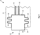
- the circuit protection ground 21 could be released from the component protection compound 20, whereby a gap 24 is formed between the two elements, in the example in Fig. 2 indicated moisture 26 can penetrate.
- the moisture 26 could be as in Fig. 2 indicated by the gap 24 towards the bonding wires 8 and the conductor tracks 15 move, of which in Fig. 2 only the tracks 15 are shown. This could corrode the bonding wires 8 and the printed conductors and thus interrupt, or migrate and thus short-circuit each other. In both cases, the magnetic field sensor 8 would be inoperable and would fail.
- the ribs 28 can be encapsulated in the application of the circuit protection compound 21 to the component protection compound 20 in a simple manner.
- the ribs 28 extend circumferentially around the magnetic field sensor 4. In this way, the sealing effect can be further increased by the ribs 28, which will be described below with reference to Fig. 3 and 4 will be explained in more detail.
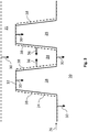
- the circuit protection mass 21 forming the circuit protection body shrinks faster with respect to the component protection mass 20. This means that the component protection mass 21 moves toward the component protection mass 20 in a radial direction 30, that is, it clamps the component protection body formed by the component protection mass 20 between itself.
- the circuit protection compound 21 applies to the radial tips 32 of the ribs 28 and thus closes the gap 24 at this point.
- Fig. 4 the conditions are shown in which the magnetic field sensor 4 is exposed to a very high temperature, which may be in the range of the operating temperature of the magnetic field sensor 4, for example.
- the axial walls 38 should be inclined with respect to a radial surface 40 of the component protection body 20 formed by the component protection body with a pitch angle between 70 ° and 88 ° ,
- circuit protection ground 21 and the component protection compound 20 further measures can be taken.
- the entire surface of the circuit protection body formed by the component protection compound 20 as shown in the WO 2010/037 810 A1 be activated, so that the formed as a polyamide circuit protection compound 21 better adheres to the surface of the circuit protection body formed by the component protection compound 20. Details can be found in the cited document.
- the activation of the surface of the circuit protection body formed by the component protection material 20 can be performed with a laser, whereby the surface of the circuit protection body formed by the component protection compound 20 further increases and the adhesion conditions for the circuit protection ground 21 on the formed by the component protection material 20 circuit protection body further improved.
Landscapes
- Engineering & Computer Science (AREA)
- Physics & Mathematics (AREA)
- Microelectronics & Electronic Packaging (AREA)
- General Physics & Mathematics (AREA)
- Manufacturing & Machinery (AREA)
- Condensed Matter Physics & Semiconductors (AREA)
- Casings For Electric Apparatus (AREA)
- Transmission And Conversion Of Sensor Element Output (AREA)
- Structures Or Materials For Encapsulating Or Coating Semiconductor Devices Or Solid State Devices (AREA)
- Gyroscopes (AREA)
- Measuring Magnetic Variables (AREA)
- Injection Moulding Of Plastics Or The Like (AREA)
- Investigating Or Analyzing Materials By The Use Of Magnetic Means (AREA)
- Measuring Fluid Pressure (AREA)
- General Engineering & Computer Science (AREA)
- Shielding Devices Or Components To Electric Or Magnetic Fields (AREA)
- Testing Of Short-Circuits, Discontinuities, Leakage, Or Incorrect Line Connections (AREA)
Description
- Die Erfindung betrifft einen Sensor zum Ausgeben eines elektrischen Signals basierend auf einer erfassten physikalischen Größe und ein Verfahren zum Herstellen eines Sensors zum Ausgeben eines elektrischen Signals basierend auf einer erfassten physikalischen Größe.
- Aus der
WO 2010 / 037 810 A1 ist ein Sensor zum Ausgeben eines elektrischen Signals basierend auf einer erfassten physikalischen Größe bekannt. Der Sensor weist eine Messschaltung auf, die in einem Schaltungsgehäuse eingehaust ist. Aus derDE 4237870 A1 ist ein ähnlicher Sensor bekannt. Es ist Aufgabe der Erfindung, den bekannten Sensor zu verbessern. - Die Aufgabe wird durch die Merkmale der unabhängigen Ansprüche gelöst. Bevorzugte Weiterbildungen sind Gegenstand der abhängigen Ansprüche.
- Gemäß einem Aspekt der Erfindung umfasst ein Sensor zum Ausgeben eines elektrischen Signals basierend auf einer erfassten physikalischen Größe eine Messschaltung, die in einem Schaltungsgehäuse eingehaust und über einen elektrischen Signalanschluss mit einer externen Schaltung kontaktierbar ist, und einen das Schaltungsgehäuse umgebenden Schutzkörper aus einer Schutzmasse mit einer Öffnung, über die ein Teil des Schaltungsgehäuses freigelegt ist. Dabei weist das Schaltungsgehäuse auf seiner Oberfläche ein Formelement auf, das von der Schutzmasse umgeben ist.
- Dem angegebenen Sensor liegt die Überlegung zugrunde, dass die Schutzmasse und das Schaltungsgehäuse Wärmeausdehnungseffekten unterworfen sind, aufgrund derer sich die Schutzmasse des Schutzkörpers vom Schaltungsgehäuse lösen und so einen Spalt zwischen dem Schutzkörper und dem Schaltungsgehäuse ausbilden könnte. In diesen Spalt könnten Feuchtigkeit und andere Reagenzien eindringen, die nach einer längeren Betriebsdauer des Sensors zu einer Korrosion oder einer Migration des Sensors im Bereich des Signalanschlusses führen und so den Signalanschluss entsprechend unterbrechen oder kurzschließen könnte.
- Diese Überlegung zugrunde gelegt ist es Idee des angegebenen Sensors, den Weg im Spalt für die oben genannte Feuchtigkeit und Reagenzien so lang wie möglich auszugestalten. Dazu sind auf der Oberfläche des Schaltungsgehäuses mindestens zwei umfänglich um das Schaltungsgehäuse verlaufende Rippen ausgebildet, die von der Schutzmasse des Schutzkörpers umgeben sind. Das heißt, dass das Schaltungsgehäuse und der Schutzkörper ineinander verzahnt werden und so den oben genannten Spalt verlängern. Die Feuchtigkeit und den Reagenzien müssen daher einen längeren Weg durch den Spalt zurücklegen, bevor die den Signalanschluss erreichen. Auf diese Weise kann die Betriebsdauer des angegebenen Sensors bis zur oben genannten Korrosion oder Migration gesteigert werden, so dass eine Ausfallrate des angegebenen Sensors gesenkt werden kann. Dabei verläuft das Formelement bzw. verlaufen die Rippen umfänglich um das Schaltungsgehäuse. Hier liegt die Überlegung zugrunde, dass der oben genannte Spalt nur deshalb zustande kommt, weil sich das Schaltungsgehäuse und der Schutzkörper wie bereits erwähnt mit unterschiedlichen Ausdehnungskoeffizienten ausdehnen. Die vorliegende Weiterbildung nutzt diese Tatsache, dass sich das Schaltungsgehäuse und der Schutzkörper aufgrund des Formelementes ineinander verzahnen. Das heißt, dass einer der beiden Verzahnungspartner das Schaltungsgehäuse oder der Schutzkörper eine Ausnehmung aufweisen und der entsprechend andere der beiden Verzahnungspartner einen Vorsprung, der im Wesentlichen formschlüssig in der Ausnehmung aufgenommen ist. Da der Schutzkörper einen höheren Ausdehnungskoeffizienten aufweist, als das Schaltungsgehäuse, wird er sich bei Kälte gegenüber dem Schaltungsgehäuse zusammenziehen und sein Verzahnungspartner wird den Verzahnungspartner am Schaltungsgehäuse radial verschließen. Bei Wärme wird sich der Schutzkörper gegenüber dem Schaltungsgehäuse ausdehnen und sein Verzahnungspartner wird den Verzahnungspartner am Schaltungsgehäuse axial verschließen. Da das Formelement / die Rippen als Verzahnungspartner am Schaltungsgehäuse daher umfänglich um dieses herum verläuft / verlaufen, kann der obige Spalt unabhängig von Wärme und Kälte in der zuvor beschriebenen Weise zuverlässig verschlossen werden.
- Zwar kann das Formelement prinzipiell eine Vertiefung im Schaltungsgehäuse sein, erfindungsgemäss sind jedoch mindestens zwei Rippen vorgesehen, die fertigungstechnisch an das Schaltungsgehäuse besonders einfach anzubringen und in einfacher Weise umspritzt oder umgossen werden können. Dabei weist die Schutzmasse einen Ausdehnungskoeffizienten auf, der größer ist, als ein Ausdehnungskoeffizient des Schaltungsgehäuses, wodurch in der oben beschriebenen Weise erreicht werden kann, dass der Spalt zwischen dem Schaltungsgehäuse und dem Schutzkörper unabhängig von Kälte oder Wärme zuverlässig verschlossen werden kann.
- In einer besonders bevorzugten Weiterbildung des angegebenen Sensors weist eine Wand des Formelements / der Rippen einen Steigungswinkel zur Oberfläche des Schaltungsgehäuses auf, der in einem Bereich zwischen 70° und 88° liegt. Mit diesem Steigungswinkel ist eine besonders effektive wärme- und kälteunabhängige Abdichtung des oben genannten Spaltes in der beschriebenen Weise gegeben.
- In einer anderen Weiterbildung des angegebenen Sensors ist die Schutzmasse um das Schaltungsgehäuse spritzbar oder vergießbar, wobei deren Schrumpfung beim Aushärten nach dem Spritzen oder Vergießen kleiner gewählt ist, als eine Schrumpfung beim Abkühlen von einer Arbeitstemperatur des Sensors auf eine Erstarrungstemperatur der Schutzmasse. Auf diese Weise ist sichergestellt, dass sich die Schutzmasse auch beim Erstarren an einen Teil des Formelementes des Schaltungsgehäuses anlegt und den Spalt so zuverlässig in der oben beschriebenen Weise verschließt.
- In einer noch anderen Weiterbildung des angegebenen Sensors ist wenigstens ein Teil der Oberfläche des Schaltungsgehäuses im Kontaktbereich mit der Schutzmasse aktiviert. Unter einer Aktivierung der Oberfläche des Schaltungsgehäuses soll nachstehend eine teilweise Zerstörung der molekularen Struktur der Oberfläche des Schaltungsgehäuses verstanden werden, so dass an der Oberfläche des Schaltungsgehäuses freie Radikale entstehen. Diese freien Radikale sind in der Lage, chemische und/oder physische Verbindungen mit der Schutzmasse einzugehen, so dass diese sich nicht mehr von der Oberfläche des Schaltungsgehäuses lösen kann. Auf diese Weise kann die Entstehung des oben genannten Spaltes fast vollständig vermieden werden. Tritt er dennoch auf, so verhindern die zuvor genannten Maßnahmen wirksam, dass die oben genannte Feuchtigkeit und Reagenzien durch den Spalt zum Signalanschluss des Sensors gelangen.
- Die Schutzmasse kann dabei ein polares Material, wie Polyamid umfassen. Das polare Polyamid kann sich in einer dem Fachmann bekannten Weise physikalisch mit der aktivierten Oberfläche des Schaltungsgehäuses verbinden und so den obigen Spalt verschließen. Es sind weitere Verbindungen möglich, die im Schmelzzustand der Schutzmasse eine polare Oberfläche aufweisen und dadurch eine Verbindung mit der aktivierten Oberfläche des Schaltungsgehäuses eingehen. Diese eingegangene Verbindung bleibt nach der Erstarrung der geschmolzenen Schutzmasse erhalten.
- In einer zusätzlichen Weiterbildung des angegebenen Sensors ist wenigstens ein Teil der Oberfläche des Schaltungsgehäuses im Kontaktbereich mit der Schutzmasse aufgeraut, so dass die wirksame aktivierte Oberfläche vergrößert und die Haftwirkung zwischen Schaltungsgehäuse und Schutzmasse gesteigert wird.
- In einer besonderen Weiterbildung des angegebenen Sensors ist der aufgeraute Teil der Oberfläche des Schaltungsgehäuses mit einem Laser aufgeraut. Mit dem Laser kann die Oberfläche des Schaltungsgehäuses nicht nur aktiviert werden, durch den Laser werden von der Oberfläche des Schaltungsgehäuses auch eventuell vorhandene Formtrennmittel abgetragen, die eine Haftung zwischen dem Schaltungsgehäuse und der Schutzmasse unterdrücken könnten.
- Alternativ kann der Laser aber auch nur zum Aufrauen der Oberfläche verwendet werden. Die Aktivierung kann dann beispielsweise mit einem Plasma durchgeführt werden.
- Gemäß einem weiteren Aspekt der Erfindung umfasst ein Verfahren zur Herstellung eines Sensors zum Ausgeben eines elektrischen Signals basierend auf einer erfassten physikalischen Größe die Schritte, die in Anspruch 7 definiert sind. Durch ein Aufrauen der Oberfläche nach einer bevorzugten Weiterbildung werden zumindest kleine Formelemente geschaffen, mit denen das Eindringen von Feuchtigkeit und Reagenzien in den Spalt weiter hinausgezögert werden kann, um die Lebensdauer des hergestellten Sensors zu erhöhen.
- Besonders bevorzugt erfolgt das Aufrauen dabei mittels eines Lasers.
- Die oben beschriebenen Eigenschaften, Merkmale und Vorteile dieser Erfindung sowie die Art und Weise, wie diese erreicht werden, werden klarer und deutlicher verständlich im Zusammenhang mit der folgenden Beschreibung der Ausführungsbeispiele, die im Zusammenhang mit den Zeichnungen näher erläutert werden, wobei:
-
Fig. 1 in einer Schnittansicht eine Schaltung mit einem Sensor, -
Fig. 2 in einer schematischen Ansicht den einen Teil des Sensors ausFig. 1 , -
Fig. 3 einen Ausschnitt aus dem Sensor ausFig. 2 , und -
Fig. 4 einen weiteren Ausschnitt aus dem Sensor ausFig. 2 zeigen. - In den Figuren werden gleiche technische Elemente mit gleichen Bezugszeichen versehen und nur einmal beschrieben.
- Es wird auf
Fig. 1 Bezug genommen, die in einer Schnittansicht eine Schaltung 2 mit einem Sensor 4 zeigt. - Der Sensor 4 ist in der vorliegenden Ausführung als Magnetfeldsensor ausgeführt, wie er beispielsweise in Drehzahlsensoren zur Erfassung eines gerasterten Magnetfeldes zum Einsatz kommt. Der Magnetfeldsensor 4 weist einen Messaufnehmer 6, wie beispielsweise einen Hallsensor oder einen an sich bekannten magnetoresistiven Messaufnehmer und eine mit dem Messaufnehmer 6 über Bonddrähte 8 verbundene Auswerteschaltung 10 auf. Dabei können der Messaufnehmer 6 und seine Auswerteschaltung 10 in einem gemeinsamen Bauteil zusammengefasst sein. Der Messaufnehmer 6 und die Auswerteschaltung 10 sind auf einem Leadframe 12 gehalten, wobei die Auswerteschaltung 10 über Bonddrähte 8 mit dem Leadframe elektrisch kontaktiert ist. Auf einer dem Messaufnehmer 6 gegenüberliegenden Seite des Leadframes 12 kann optional ein Magnet 14 gehalten sein, der in einer dem Fachmann bekannten Weise einen Arbeitspunkt für den Messaufnehmer 6 festlegt, wenn dies für den Einsatz wie bei einigen magnetoresistiven Messaufnehmern notwendig ist.
- Über die Bonddrähte 8 können Messsignale aus dem Messaufnehmer 6, wie beispielsweise eine Hallspannung aus einem als Hallsensor ausgebildeten Messaufnehmer 6 übertragen werden. Die Messsignale können in der Auswerteschaltung 10 gefiltert, gewandelt und codiert werden. Die durch die Auswerteschaltung 10 ausgewerteten Messsignale können dann über die Bonddrähte zwischen der Auswerteschaltung 10 und dem Leadframe 12 auf Leiterbahnen 15 des Leadframes 12 übertragen werden, die die ausgewerteten Messsignale dann beispielsweise an eine Motorsteuerung in einem Fahrzeug weiterleiten können.
- Die Leiterbahnen 15 auf des Leadframes 12 sind über Ausnehmungen 16 strukturiert und können neben dem Magnetfeldsensor 4 weitere elektrische Bauelemente wie beispielsweise ein Schutzkondensator 18 für den Magnetfeldsensor 4 tragen.
- Die einzelnen elektrischen Bauelemente 4, 18 auf dem Leadframe 12 können je von einer Bauteilschutzmasse 20 umgeben sein. Diese Bauteilschutzmasse 20 dient den elektrischen einzelnen Bauelementen 4, 18 als Bauteilschutzkörper, der die elektrischen Bauelemente 4, 18 beispielsweise bei der Montage auf dem Leadframe 12 vor einem unbeabsichtigten Berühren schützt.
- Die Gesamtheit aller elektrischen Bauelemente 4, 18 ist in der vorliegenden Ausführung von einer Schaltungsschutzmasse 21 umgeben, um die basierend auf dem Leadframe 12, den Leiterbahnen 15 und den elektrischen Bauelementen 4, 18 ausgebildete Schaltung vor Schmutz und Feuchtigkeit zu schützen und ihre Lebensdauer zu steigern.
- Dabei sollte jedoch zur Herstellung des Schaltungsschutzkörpers so wenig wie möglich Schaltungsschutzmasse 21 verwendet werden, weshalb es günstig wäre, einen Teil der Bauteilschutzmasse 20 der elektrischen Bauelemente 4, 18 nicht mit der Schaltungsschutzmasse 21 zu bedecken.
- Wird beispielsweise ein Teil der Bauteilschutzmasse 20 des Magnetfeldsensors 4 nicht mit der Schaltungsschutzmasse 21 bedeckt, dann weist der durch die Schaltungsschutzmasse 20 ausgebildete Schaltungsschutzkörper eine Öffnung 22 auf.
- Diese Öffnung 22 ist kann jedoch problematisch sein, da der Magnetfeldsensor 4 prinzipbedingt Temperaturschwankungen ausgesetzt ist, die zu unterschiedlichen Wärmeausdehnungen der Bauteilschutzmasse 20 und der Schaltungsschutzmasse 21 führen können. Umfasst die Bauteilschutzmasse 20 beispielsweise ein Duroplastmaterial, wie beispielsweise einem Epoxidharz und wird von einem Thermoplast als Schaltungsschutzmasse 21, wie beispielsweise einem Polyamid umhüllt, dann dehnt sich das Polyamid aufgrund eines höheren Wärmeausdehnungskoeffizienten schneller aus, als das Epoxidharz. In diesem Fall könnte sich die Schaltungsschutzmasse 21 von der Bauteilschutzmasse 20 lösen, wodurch sich zwischen beiden Elementen ein Spalt 24 ausbildet, in den beispielsweise in
Fig. 2 angedeutete Feuchtigkeit 26 eindringen kann. - Dies soll anhand von
Fig. 2 näher erläutert werden, die in einer schematischen Ansicht einen Teil des Magnetfeldsensors 4 ausFig. 1 zeigt. - Die Feuchtigkeit 26 könnte sich wie in
Fig. 2 angedeutet durch den Spalt 24 hin zu den Bonddrähten 8 und den Leiterbahnen 15 bewegen, von denen inFig. 2 nur die Leiterbahnen 15 gezeigt sind. Dies könnte die Bonddrähte 8 und die Leiterbahnen korrodieren und so unterbrechen, oder migrieren und so gegeneinander kurzschließen. In beiden Fällen wäre der Magnetfeldsensor 8 funktionsuntüchtig und würde ausfallen. - Um das Erreichen der Feuchtigkeit 26 an den Bonddrähten 8 und Leiterbahnen 15 soweit wie möglich hinauszuzögern, sind in der vorliegenden Ausführung an der Bauteilschutzmasse 20 Formelemente in Form von Rippen 28 ausgebildet, die die Feuchtigkeit 26 in dem Spalt 24 umfließen muss. Auf diese Weise wird für die Feuchtigkeit 26 der Weg durch den Spalt 24 verlängert, was die oben genannten Folgen der Feuchtigkeit 26 an den Bonddrähten 8 und den Leiterbahnen 15 hinauszögert und der Magnetfeldsensor 8 so länger betriebsfähig bleiben kann.
- Die Rippen 28 können beim Aufbringen der Schaltungsschutzmasse 21 auf die Bauteilschutzmasse 20 in einfacher Weise umspritzt werden. Dabei verlaufen die Rippen 28 umfänglich um den Magnetfeldsensor 4. Auf diese Weise kann die Dichtwirkung durch die Rippen 28 weiter gesteigert werden, was nachstehend anhand der
Fig. 3 und4 näher erläutert werden soll. - Anhand
Fig. 3 soll der Spalt 24 zwischen der Bauteilschutzmasse 20 und der Schaltungsschutzmasse 21 beschrieben werden, wenn der Magnetfeldsensor 4 einer sehr niedrigen Temperatur, ausgesetzt ist, die beispielsweise deutlich niedriger ist, als eine Betriebstemperatur des Magnetfeldsensors 4. - In dem Magnetfeldsensor 4 schrumpft die den Schaltungsschutzkörper bildende Schaltungsschutzmasse 21 gegenüber der Bauteilschutzmasse 20 schneller. Das heißt, dass sich die Bauteilschutzmasse 21 in einer radialen Richtung 30 auf die Bauteilschutzmasse 20 zubewegt, das heißt, sie klemmt die den durch die Bauteilschutzmasse 20 gebildeten Bauteilschutzkörper zwischen sich ein. Somit legt sich die Schaltungsschutzmasse 21 auf die radialen Spitzen 32 der Rippen 28 und verschließt so den Spalt 24 an dieser Stelle. Zwar zieht sich eine zwischen den Rippen 28 eingreifende Zunge 34 aus der Schaltungsschutzmasse 21 in axialer Richtung 36 zusammen und öffnet damit den Spalt 24 an den axialen Wänden 38 der Rippen 28, es existiert jedoch kein durchgehender Spalt 24 zu den Leiterbahnen 15 und den Bonddrähten 8, so dass dorthin auch keine Feuchtigkeit 26 eindringen kann.
- In
Fig. 4 sind die Verhältnisse gezeigt, in denen der Magnetfeldsensor 4 einer sehr hohen Temperatur, ausgesetzt ist, die beispielsweise im Bereich der Betriebstemperatur des Magnetfeldsensors 4 liegen kann. - In diesem Fall dehnt sich zwar die gesamte Schaltungsschutzmasse 21 aus und löst sich in radialer Richtung 30 beispielsweise von den radialen Spitzen 32 der Rippen 28, jedoch dehnt sich auch gleichzeitig die Zunge 34 in axialer Richtung 36 aus und verschließt so den Spalt 24 an den axialen Wänden 38 der Rippen, so dass auch in diesem Fall kein durchgehender Spalt 24 bis zu den Bonddrähten 8 vorhanden ist.
- Um in diesem Falle eine besonders gute Verschlusswirkung des Spaltes 24 an den axialen Wänden 38 der Rippen 28 zu erzielen, sollten die axialen Wände 38 gegenüber einer radialen Oberfläche 40 des durch die Bauteilschutzmasse 20 gebildeten Bauteilschutzkörpers mit einem Steigungswinkel zwischen 70° und 88° geneigt sein.
- Zur Verbesserung der Haftwirkung zwischen der Schaltungsschutzmasse 21 und der Bauteilschutzmasse 20 können weitere Maßnahmen ergriffen werden. So kann beispielsweise die gesamte Oberfläche des durch die Bauteilschutzmasse 20 gebildeten Schaltungsschutzkörpers wie in der
WO 2010 / 037 810 A1 aktiviert werden, so dass die als Polyamid ausgebildete Schaltungsschutzmasse 21 besser an der Oberfläche des durch die Bauteilschutzmasse 20 gebildeten Schaltungsschutzkörpers haftet. Details dazu können der genannten Druckschrift entnommen werden. - Ferner kann die Aktivierung der Oberfläche des durch die Bauteilschutzmasse 20 gebildeten Schaltungsschutzkörpers mit einem Laser durchgeführt werden, wodurch die Oberfläche des durch die Bauteilschutzmasse 20 gebildeten Schaltungsschutzkörpers weiter vergrößert und die Haftbedingungen für die Schaltungsschutzmasse 21 am durch die Bauteilschutzmasse 20 gebildeten Schaltungsschutzkörper weiter verbessert werden.
Claims (9)
- Sensor (4) zum Ausgeben eines elektrischen Signals basierend auf einer erfassten physikalischen Größe, umfassend:- eine Messschaltung (6, 10), die in einem Schaltungsgehäuse (20) eingehaust und über einen elektrischen Signalanschluss (8) mit einer externen Schaltung (12) kontaktierbar ist, und- einen das Schaltungsgehäuse (20) umgebenden Schutzkörper aus einer Schutzmasse (21) mit einer Öffnung (22), über die ein Teil des Schaltungsgehäuses (20) freigelegt ist,- wobei das Schaltungsgehäuse (20) auf seiner Oberfläche mindestens zwei umfänglich um das Schaltungsgehäuse (20) verlaufende Rippen (28) aufweist, die von der Schutzmasse (21) umgeben sind, und- wobei die Schutzmasse (21) einen Ausdehnungskoeffizienten aufweist, der größer ist als ein Ausdehnungskoeffizient des Schaltungsgehäuses (20).
- Sensor (4) nach Anspruch 1, wobei eine Wand (38) der Rippen (28) einen Steigungswinkel (42) zur Oberfläche (40) des Schaltungsgehäuses (20) in einem Bereich zwischen 70° und 88° aufweist.
- Sensor (4) nach einem der vorstehenden Ansprüche, wobei die Schutzmasse (21) um das Schaltungsgehäuse (20) spritzbar oder vergießbar ist, wobei deren Schrumpfung beim Aushärten nach dem Spritzen oder Vergießen kleiner gewählt ist, als eine Schrumpfung beim Abkühlen von einer Erstarrungstemperatur der Schutzmasse (21) auf eine Betriebstemperatur des Sensors (4).
- Sensor (4) nach einem der vorstehenden Ansprüche, wobei wenigstens ein Teil der Oberfläche des Schaltungsgehäuses (20) im Kontaktbereich mit der Schutzmasse (21) aktiviert ist.
- Sensor (4) nach einem der vorstehenden Ansprüche, wobei wenigstens ein Teil der Oberfläche des Schaltungsgehäuses (20) im Kontaktbereich mit der Schutzmasse (21) aufgeraut ist.
- Sensor nach Anspruch 5, wobei der aufgeraute Teil der Oberfläche des Schaltungsgehäuses (20) mit einem Laser aufgeraut ist.
- Verfahren zur Herstellung eines Sensors (4) zum Ausgeben eines elektrischen Signals basierend auf einer erfassten physikalischen Größe, umfassend die Schritte:- Einhausen einer Messschaltung (6, 10), die über einen elektrischen Signalanschluss (8) mit einer externen Schaltung (12) kontaktierbar ist, in einem Schaltungsgehäuse (20), wobei das Schaltungsgehäuse auf seiner Oberfläche mindestens zwei umfänglich um das Schaltungsgehäuse verlaufende Rippen (28) aufweist,- Einhausen des Schaltungsgehäuses (20) mit einer Schutzmasse (21), deren Ausdehnungskoeffizient größer ist als ein Ausdehnungskoeffizient des Schaltungsgehäuses (20).
- Verfahren nach Anspruch 7, gekennzeichnet durch den Schritt:- Aufrauen wenigstens eines Teils der Oberfläche des Schaltungsgehäuses (20), insbesondere mit einem Laser.
- Verfahren nach Anspruch 7 oder 8, dadurch gekennzeichnet, dass die Schutzmasse wenigstens im Bereich der aufgerauten Oberfläche aufgebracht wird.
Applications Claiming Priority (2)
| Application Number | Priority Date | Filing Date | Title |
|---|---|---|---|
| DE102012224102 | 2012-12-20 | ||
| PCT/EP2013/075186 WO2014095314A1 (de) | 2012-12-20 | 2013-11-29 | Sensor zum ausgeben eines elektrischen signals basierend auf einer erfassten physikalischen grösse |
Publications (2)
| Publication Number | Publication Date |
|---|---|
| EP2936074A1 EP2936074A1 (de) | 2015-10-28 |
| EP2936074B1 true EP2936074B1 (de) | 2017-05-10 |
Family
ID=49681044
Family Applications (3)
| Application Number | Title | Priority Date | Filing Date |
|---|---|---|---|
| EP13799037.0A Ceased EP2936076A2 (de) | 2012-12-20 | 2013-11-29 | Elektronische vorrichtung und verfahren zur herstellung einer elektronischen vorrichtung |
| EP13798670.9A Active EP2936074B1 (de) | 2012-12-20 | 2013-11-29 | Sensor zum ausgeben eines elektrischen signals basierend auf einer erfassten physikalischen grösse |
| EP13799036.2A Ceased EP2936075A1 (de) | 2012-12-20 | 2013-11-29 | Elektronische vorrichtung und verfahren zur herstellung einer elektronischen vorrichtung |
Family Applications Before (1)
| Application Number | Title | Priority Date | Filing Date |
|---|---|---|---|
| EP13799037.0A Ceased EP2936076A2 (de) | 2012-12-20 | 2013-11-29 | Elektronische vorrichtung und verfahren zur herstellung einer elektronischen vorrichtung |
Family Applications After (1)
| Application Number | Title | Priority Date | Filing Date |
|---|---|---|---|
| EP13799036.2A Ceased EP2936075A1 (de) | 2012-12-20 | 2013-11-29 | Elektronische vorrichtung und verfahren zur herstellung einer elektronischen vorrichtung |
Country Status (9)
| Country | Link |
|---|---|
| US (3) | US9615469B2 (de) |
| EP (3) | EP2936076A2 (de) |
| JP (3) | JP6302928B2 (de) |
| KR (4) | KR102135491B1 (de) |
| CN (4) | CN104870946B (de) |
| BR (2) | BR112015014233B1 (de) |
| DE (4) | DE102013217888B4 (de) |
| MX (2) | MX348915B (de) |
| WO (4) | WO2014095316A2 (de) |
Families Citing this family (6)
| Publication number | Priority date | Publication date | Assignee | Title |
|---|---|---|---|---|
| FR3055737B1 (fr) * | 2016-09-08 | 2018-11-30 | Continental Automotive France | Procede de fabrication sur une plaque de maintien metallique d'au moins un module electronique incluant au moins un test electrique |
| JP2018151304A (ja) * | 2017-03-14 | 2018-09-27 | エイブリック株式会社 | 磁気センサ回路、検査方法、及び製造方法 |
| CN108964251A (zh) * | 2018-04-17 | 2018-12-07 | 黑龙江博瑞特高新技术开发有限公司 | 基于mems技术的双电源开关监控的测试方法 |
| DE102018207694B4 (de) * | 2018-05-17 | 2020-10-08 | Audi Ag | Hochvoltkomponente zum Anordnen in einem Hochvoltbordnetz eines Kraftfahrzeugs, Kraftfahrzeug und Verfahren zum Schützen einer Hochvoltkomponente |
| DE102019210373A1 (de) * | 2019-07-12 | 2021-01-14 | Continental Teves Ag & Co. Ohg | Sensor mit dichter Umspritzung und einem freigestellten Bereich |
| DE102019210375A1 (de) * | 2019-07-12 | 2021-01-14 | Continental Teves Ag & Co. Ohg | Verfahren zur Herstellung eines robusten Sensors |
Family Cites Families (101)
| Publication number | Priority date | Publication date | Assignee | Title |
|---|---|---|---|---|
| DD50658A1 (de) | 1965-07-27 | 1966-10-05 | Peter Kolodziej | Baustein mit integrierter Schaltung in Dünnfilmtechnik |
| JPS5326670A (en) * | 1976-08-25 | 1978-03-11 | Hitachi Ltd | Manufacture of semiconductor device |
| US4295117A (en) | 1980-09-11 | 1981-10-13 | General Motors Corporation | Pressure sensor assembly |
| DE3243132C2 (de) * | 1982-11-22 | 1985-06-27 | Siemens AG, 1000 Berlin und 8000 München | Kastenförmige Flachbaugruppe |
| JPS59202652A (ja) * | 1983-04-30 | 1984-11-16 | Mitsubishi Electric Corp | 半導体装置の製造方法 |
| DE3506639A1 (de) * | 1985-02-26 | 1986-08-28 | Thielmann-Luwa GmbH, 5920 Bad Berleburg | Transport- und/oder lagerbehaelter mit datentraeger |
| JP2569717B2 (ja) * | 1987-06-05 | 1997-01-08 | 日本電装株式会社 | 樹脂封止型半導体装置およびその製造方法 |
| DE3913966B4 (de) * | 1988-04-28 | 2005-06-02 | Ibiden Co., Ltd., Ogaki | Klebstoffdispersion zum stromlosen Plattieren, sowie Verwendung zur Herstellung einer gedruckten Schaltung |
| US4994895A (en) * | 1988-07-11 | 1991-02-19 | Fujitsu Limited | Hybrid integrated circuit package structure |
| JPH04268789A (ja) | 1991-02-23 | 1992-09-24 | Taiyo Yuden Co Ltd | 混成集積回路装置及びその製造方法 |
| DE4141958A1 (de) * | 1991-12-19 | 1993-06-24 | Swf Auto Electric Gmbh | Drehzahlsensor, insbesondere zahnradsensor |
| DE9202995U1 (de) * | 1992-03-06 | 1992-06-11 | Aug. Winkhaus GmbH & Co KG, 4404 Telgte | Flachschlüssel |
| JPH0613475A (ja) | 1992-04-28 | 1994-01-21 | Matsushita Electric Ind Co Ltd | 符号を備えた電子部品とプリント配線基板と電子機器と符号の形成方法 |
| US5386730A (en) | 1992-06-25 | 1995-02-07 | Nippondenso Co., Ltd. | Pressure sensor having a sealed water-resistant construction |
| US5598034A (en) * | 1992-07-22 | 1997-01-28 | Vlsi Packaging Corporation | Plastic packaging of microelectronic circuit devices |
| JP2851491B2 (ja) * | 1992-08-13 | 1999-01-27 | 三菱電機株式会社 | 内燃機関用点火装置 |
| DE4237870A1 (de) | 1992-11-10 | 1994-03-10 | Daimler Benz Ag | Verfahren zur Herstellung eines elektronischen Steuergeräts für ein Kraftfahrzeug, und nach diesem Verfahren herstellbares Steuergerät |
| US5557066A (en) * | 1993-04-30 | 1996-09-17 | Lsi Logic Corporation | Molding compounds having a controlled thermal coefficient of expansion, and their uses in packaging electronic devices |
| US5383788A (en) * | 1993-05-20 | 1995-01-24 | W. L. Gore & Associates, Inc. | Electrical interconnect assembly |
| US5656782A (en) * | 1994-12-06 | 1997-08-12 | The Foxboro Company | Pressure sealed housing apparatus and methods |
| TW323432B (de) * | 1995-04-28 | 1997-12-21 | Victor Company Of Japan | |
| JP3127812B2 (ja) * | 1995-12-27 | 2001-01-29 | 株式会社デンソー | 電気回路装置の封止構造 |
| DE19612765A1 (de) * | 1996-03-29 | 1997-11-13 | Teves Gmbh Alfred | Kunststoffsensor und Verfahren zu dessen Herstellung |
| KR100498821B1 (ko) * | 1996-03-29 | 2005-11-11 | 아이티티 매뉴팩츄어링 엔터프라이즈, 인코포레이티드 | 플라스틱센서및그제조방법 |
| US5948991A (en) | 1996-12-09 | 1999-09-07 | Denso Corporation | Semiconductor physical quantity sensor device having semiconductor sensor chip integrated with semiconductor circuit chip |
| JP3671563B2 (ja) * | 1996-12-09 | 2005-07-13 | 株式会社デンソー | モールドicをケースに固定した構造の半導体装置 |
| DE19709364C2 (de) * | 1997-03-07 | 1998-12-24 | Diehl Ident Gmbh | Plombe für ein geteiltes Gehäuse |
| US6003369A (en) * | 1997-05-19 | 1999-12-21 | Continental Teves, Inc. | Method for manufacturing encapsulated semiconductor devices |
| US5927484A (en) * | 1997-05-28 | 1999-07-27 | Eaton Corporation | Circuit breaker with welded contact interlock, gas sealing cam rider and double rate spring |
| JP3284925B2 (ja) * | 1997-06-03 | 2002-05-27 | 株式会社デンソー | 点火装置 |
| US5963028A (en) | 1997-08-19 | 1999-10-05 | Allegro Microsystems, Inc. | Package for a magnetic field sensing device |
| US6178359B1 (en) | 1998-03-31 | 2001-01-23 | Tektronix, Inc. | Instrument with installation-evident accessory modules |
| US6286207B1 (en) * | 1998-05-08 | 2001-09-11 | Nec Corporation | Resin structure in which manufacturing cost is cheap and sufficient adhesive strength can be obtained and method of manufacturing it |
| JP2000074694A (ja) * | 1998-08-27 | 2000-03-14 | Hitachi Ltd | 回転センサの異常検出装置及び異常検出方法 |
| US6221459B1 (en) | 1998-11-30 | 2001-04-24 | Intel Corporation | Controlling the heat expansion of electrical couplings |
| DE20017105U1 (de) | 2000-10-04 | 2001-01-18 | Siemens AG, 80333 München | Schaltungsanordnung |
| DE10146949A1 (de) | 2000-11-22 | 2002-06-06 | Continental Teves Ag & Co Ohg | Aktiver Magnetsensor für elektronische Bremssysteme |
| US20020170897A1 (en) * | 2001-05-21 | 2002-11-21 | Hall Frank L. | Methods for preparing ball grid array substrates via use of a laser |
| JP3809353B2 (ja) | 2001-08-02 | 2006-08-16 | キヤノン株式会社 | Id付き加工物の製造方法 |
| JP2003098213A (ja) * | 2001-09-20 | 2003-04-03 | Oht Inc | 検査装置並びに検査方法 |
| JP3832641B2 (ja) * | 2001-12-14 | 2006-10-11 | シャープ株式会社 | 半導体装置、積層型半導体装置及び半導体装置の製造方法 |
| DE10207762A1 (de) | 2002-02-23 | 2003-09-04 | Endress & Hauser Gmbh & Co Kg | Elektrotechnisches Gerät |
| US20040051211A1 (en) * | 2002-09-12 | 2004-03-18 | Xerox Corporation | Production of seamless belts and seamless belt products |
| US7417315B2 (en) | 2002-12-05 | 2008-08-26 | International Business Machines Corporation | Negative thermal expansion system (NTEs) device for TCE compensation in elastomer composites and conductive elastomer interconnects in microelectronic packaging |
| JP2004198240A (ja) * | 2002-12-18 | 2004-07-15 | Denso Corp | センサ装置 |
| DE10300171A1 (de) | 2003-01-08 | 2004-07-22 | Hella Kg Hueck & Co. | Elektronische Baugruppe mit metallischem Gehäuseteil |
| DE10300175B4 (de) | 2003-01-08 | 2016-12-29 | Hella Kgaa Hueck & Co. | Elektronische Baugruppe mit Wärme ableitendem Gehäuseteil |
| DE10313832A1 (de) | 2003-03-21 | 2004-10-14 | Tyco Electronics Pretema Gmbh | Baueinheit und Verfahren zur Herstellung einer Baueinheit |
| JP4197140B2 (ja) * | 2003-06-19 | 2008-12-17 | パナソニック株式会社 | 半導体装置 |
| US6953891B2 (en) * | 2003-09-16 | 2005-10-11 | Micron Technology, Inc. | Moisture-resistant electronic device package and methods of assembly |
| JP4300521B2 (ja) * | 2004-02-12 | 2009-07-22 | 富士フイルム株式会社 | 電磁誘導タグ及び部品選択システム並びに部品選択方法 |
| DE102004015597B4 (de) * | 2004-03-30 | 2007-12-06 | Qimonda Ag | Halbleitervorrichtung mit schützender Gehäusestruktur |
| JP2006222406A (ja) * | 2004-08-06 | 2006-08-24 | Denso Corp | 半導体装置 |
| DE202004020518U1 (de) * | 2004-08-13 | 2006-04-06 | Robert Bosch Gmbh | Akkuschrauber |
| EP1630913B1 (de) | 2004-08-31 | 2007-10-03 | Infineon Technologies AG | Verfahren zum Herstellen eines mit einem Kunststoffgehäuse versehenen optischen oder elektronischen Moduls das eine optische oder elektronische Komponente enthält, sowie optisches oder elektronisches Modul |
| DE102004054622A1 (de) * | 2004-11-11 | 2006-05-18 | Ksg Leiterplatten Gmbh | Schichtanordnung für eine Leiterplatte |
| JP2006303106A (ja) * | 2005-04-19 | 2006-11-02 | Denso Corp | 電子回路装置 |
| US9093359B2 (en) * | 2005-07-01 | 2015-07-28 | Vishay-Siliconix | Complete power management system implemented in a single surface mount package |
| WO2007025252A1 (en) * | 2005-08-26 | 2007-03-01 | Tk Holdings Inc. | Electronic module and method for sealing an electronic module |
| JP4631727B2 (ja) * | 2006-01-30 | 2011-02-16 | 株式会社デンソー | ガスセンサ |
| JP4868887B2 (ja) * | 2006-02-28 | 2012-02-01 | パナソニック電工Sunx株式会社 | 樹脂溶着方法、樹脂部品 |
| JP4503039B2 (ja) * | 2006-04-27 | 2010-07-14 | 三洋電機株式会社 | 回路装置 |
| WO2007138694A1 (ja) * | 2006-05-31 | 2007-12-06 | Hitachi, Ltd. | 照合方法 |
| JP5200338B2 (ja) | 2006-06-15 | 2013-06-05 | ソニー株式会社 | Rfidタグおよび商品 |
| TWI309467B (en) | 2006-06-21 | 2009-05-01 | Advanced Semiconductor Eng | Substrate strip and substrate structure and method for manufacturing the same |
| DE102006032073B4 (de) | 2006-07-11 | 2016-07-07 | Intel Deutschland Gmbh | Elektrisch leitfähiger Verbund aus einem Bauelement und einer Trägerplatte |
| DE102006032998B4 (de) | 2006-07-17 | 2010-09-16 | Continental Automotive Gmbh | Sensorbaugruppe mit einem Sensorband, insbesondere mit einem faseroptischen Sensorband |
| JP2008033724A (ja) * | 2006-07-31 | 2008-02-14 | Mitsumi Electric Co Ltd | シングル・チップ半導体集積回路装置の製造方法、プログラムデバッグ方法、マイクロコントローラの製造方法 |
| DE102006042556A1 (de) * | 2006-09-11 | 2008-03-27 | Siemens Ag | Elektronisches Modul, insbesondere Sensorbaugruppe, und Verfahren zum Herstellen eines elektronischen Moduls |
| JP2008172172A (ja) * | 2007-01-15 | 2008-07-24 | Denso Corp | 電子制御装置及びその製造方法 |
| US7849843B2 (en) * | 2007-04-27 | 2010-12-14 | Denso Corporation | Ignition coil |
| US20080290482A1 (en) * | 2007-05-25 | 2008-11-27 | National Semiconductor Corporation | Method of packaging integrated circuits |
| JP4380748B2 (ja) * | 2007-08-08 | 2009-12-09 | ヤマハ株式会社 | 半導体装置、及び、マイクロフォンパッケージ |
| US7830135B2 (en) | 2007-08-14 | 2010-11-09 | Fluke Corporation | Digital multimeter having housing sealing arrangement |
| US8207607B2 (en) * | 2007-12-14 | 2012-06-26 | Denso Corporation | Semiconductor device with resin mold |
| EP2154713B1 (de) * | 2008-08-11 | 2013-01-02 | Sensirion AG | Verfahren zur Herstellung einer Messvorrichtung mit einer Spannungsverminderungsschicht |
| DE102008064046A1 (de) * | 2008-10-02 | 2010-04-08 | Continental Teves Ag & Co. Ohg | Verfahren zur Herstellung eines Geschwindigkeits-Sensorelementes |
| DE102008064047A1 (de) * | 2008-10-02 | 2010-04-08 | Continental Teves Ag & Co. Ohg | Sensorelement und Trägerelement zur Herstellung eines Sensors |
| DE102008043773A1 (de) * | 2008-11-17 | 2010-05-20 | Robert Bosch Gmbh | Elektrisches und/oder mikromechanisches Bauelement und Verfahren zur Herstellung eines elektrischen und/oder mikromechanischen Bauelements |
| JP5339968B2 (ja) | 2009-03-04 | 2013-11-13 | パナソニック株式会社 | 実装構造体及びモータ |
| JP5110049B2 (ja) * | 2009-07-16 | 2012-12-26 | 株式会社デンソー | 電子制御装置 |
| EP2462616A1 (de) * | 2009-08-05 | 2012-06-13 | Continental Teves AG & Co. oHG | Sensoranordnung und chip mit zusätzlichen befestigungsbeinen |
| DE102009028956A1 (de) * | 2009-08-28 | 2011-03-03 | Robert Bosch Gmbh | Magnetfeldsensor |
| JP5075171B2 (ja) * | 2009-09-02 | 2012-11-14 | パナソニック株式会社 | 超音波センサ |
| JP2011100718A (ja) * | 2009-10-05 | 2011-05-19 | Yazaki Corp | コネクタ |
| JP2011086685A (ja) * | 2009-10-13 | 2011-04-28 | Asmo Co Ltd | 樹脂封止型半導体装置及びその製造方法 |
| JP5412357B2 (ja) * | 2010-04-01 | 2014-02-12 | 株式会社フジクラ | メンブレン配線板 |
| JP5195819B2 (ja) * | 2010-06-02 | 2013-05-15 | 株式会社デンソー | 空気流量測定装置 |
| US20120031786A1 (en) * | 2010-06-02 | 2012-02-09 | Patrick Mish | Protective skin for an e-reader |
| CN103153729B (zh) | 2010-08-10 | 2016-08-03 | 大陆-特韦斯贸易合伙股份公司及两合公司 | 用于调节行驶稳定性的方法和系统 |
| JP2012073113A (ja) * | 2010-09-29 | 2012-04-12 | Misuzu Kogyo:Kk | 化学センサー、化学センサーの製造方法 |
| DE102011004144A1 (de) | 2011-02-15 | 2012-08-16 | Robert Bosch Gmbh | Schwingungsaufnehmer und Verfahren zum Herstellen eines derartigen Schwingungsaufnehmers |
| DE102012201018B4 (de) | 2012-01-24 | 2016-03-31 | Ifm Electronic Gmbh | Messgerät mit am Gehäuse vorgesehenem Luftdurchgang |
| DE102012203222A1 (de) | 2012-03-01 | 2013-09-05 | Robert Bosch Gmbh | Gehäuseteil für eine Antriebseinheit, sowie Verfahren und Werkzeug zur Herstellung eines solchen |
| DE202012003728U1 (de) | 2012-04-15 | 2013-07-17 | Dietmar Friedrich Brück | Meldeeinrichtung zur Montage in oder an einem Element, insbesondere in einer Raumdecke |
| JP6296687B2 (ja) * | 2012-04-27 | 2018-03-20 | キヤノン株式会社 | 電子部品、電子モジュールおよびこれらの製造方法。 |
| CN104508816B (zh) * | 2012-07-30 | 2017-08-01 | 大陆-特韦斯贸易合伙股份公司及两合公司 | 用于为电子装置布线的布线设备 |
| DE102012213917A1 (de) * | 2012-08-06 | 2014-02-20 | Robert Bosch Gmbh | Bauelemente-Ummantelung für ein Elektronikmodul |
| EP2725715B1 (de) * | 2012-10-29 | 2018-12-12 | Optosys SA | Näherungssensor |
| DE102014205922B4 (de) * | 2014-03-31 | 2020-12-03 | Aktiebolaget Skf | Modul zum Erfassen eines Vibrationsverhaltens einer mechanischen Komponente |
| TWI567475B (zh) * | 2014-12-02 | 2017-01-21 | 明基電通股份有限公司 | 投影機鎖附裝置 |
-
2013
- 2013-09-06 DE DE102013217888.3A patent/DE102013217888B4/de active Active
- 2013-09-06 DE DE102013217892.1A patent/DE102013217892A1/de active Pending
- 2013-11-29 KR KR1020157018685A patent/KR102135491B1/ko active Active
- 2013-11-29 EP EP13799037.0A patent/EP2936076A2/de not_active Ceased
- 2013-11-29 JP JP2015548320A patent/JP6302928B2/ja active Active
- 2013-11-29 MX MX2015007898A patent/MX348915B/es active IP Right Grant
- 2013-11-29 JP JP2015548321A patent/JP2016507891A/ja active Pending
- 2013-11-29 WO PCT/EP2013/075188 patent/WO2014095316A2/de not_active Ceased
- 2013-11-29 CN CN201380066822.3A patent/CN104870946B/zh active Active
- 2013-11-29 DE DE102013224652.8A patent/DE102013224652A1/de not_active Withdrawn
- 2013-11-29 BR BR112015014233-8A patent/BR112015014233B1/pt active IP Right Grant
- 2013-11-29 CN CN201380066338.0A patent/CN104870945B/zh active Active
- 2013-11-29 KR KR1020157019574A patent/KR102112894B1/ko active Active
- 2013-11-29 DE DE102013224650.1A patent/DE102013224650A1/de not_active Withdrawn
- 2013-11-29 EP EP13798670.9A patent/EP2936074B1/de active Active
- 2013-11-29 WO PCT/EP2013/075187 patent/WO2014095315A1/de not_active Ceased
- 2013-11-29 BR BR112015014490-0A patent/BR112015014490B1/pt active IP Right Grant
- 2013-11-29 WO PCT/EP2013/075186 patent/WO2014095314A1/de not_active Ceased
- 2013-11-29 CN CN201380066841.6A patent/CN104884906B/zh not_active Expired - Fee Related
- 2013-11-29 US US14/651,307 patent/US9615469B2/en not_active Expired - Fee Related
- 2013-11-29 KR KR1020157019575A patent/KR102136910B1/ko active Active
- 2013-11-29 US US14/650,427 patent/US10178781B2/en active Active
- 2013-11-29 US US14/648,782 patent/US9832892B2/en active Active
- 2013-11-29 KR KR1020157017734A patent/KR102119919B1/ko not_active Expired - Fee Related
- 2013-11-29 EP EP13799036.2A patent/EP2936075A1/de not_active Ceased
- 2013-11-29 MX MX2015007897A patent/MX344003B/es active IP Right Grant
- 2013-11-29 JP JP2015548322A patent/JP6062566B2/ja active Active
- 2013-11-29 WO PCT/EP2013/075185 patent/WO2014095313A1/de not_active Ceased
- 2013-11-29 CN CN201380067259.1A patent/CN104870947B/zh active Active
Also Published As
Similar Documents
| Publication | Publication Date | Title |
|---|---|---|
| WO2014095314A1 (de) | Sensor zum ausgeben eines elektrischen signals basierend auf einer erfassten physikalischen grösse | |
| EP2880967B1 (de) | Bauelemente-ummantelung für ein elektronikmodul | |
| EP0889774B1 (de) | Kunststoffsensor und verfahren zu dessen herstellung | |
| DE102014216490B4 (de) | Verbindungselement mit eingebauter elektronischer schalttafel und verfahren zum herstellen des selben | |
| WO2013072128A1 (de) | Integrierter feuchtesensor und verfahren zu dessen herstellung | |
| EP3074730A1 (de) | Sensorherstellung durch halten des zwischenspritzlings | |
| DE102007054717B4 (de) | Transmitter und Verfahren zur Herstellung eines Transmitters | |
| DE102009046467B4 (de) | Leiterbahnstanzgitter mit einer speziellen Oberflächenkontur sowie Steuergerät mit einem solchen Leiterbahnstanzgitter | |
| DE2336727A1 (de) | Elektrischer kondensator | |
| EP1357774A1 (de) | Verfahren zum Herstellen einer kunststoffumspritzen Leiterstruktur sowie elektrische Schaltungseinheit mit einer kunststoffumspritzten Leiterstruktur | |
| DE102011000736B4 (de) | Abbrandsicherer Feuchtigkeitsschutz von Leiterplatten | |
| DE102011107110B4 (de) | Verfahren zum Umgeben eines elektrischen Bauteils mit einem Schutzgehäuse sowie elektrisches Bauteil mit einem Schutzgehäuse | |
| DE19838266A1 (de) | Einrichtung und Verfahren zum Vergießen elektrischer Schaltungen mittels Spritzguß | |
| DE102014225856A1 (de) | Sensoreinrichtung | |
| DE202014010469U1 (de) | Widerstand | |
| DE102008052399A1 (de) | Gasgenerator für eine Sicherheitseinrichtung in einem Fahrzeug | |
| EP2704544B1 (de) | Sensoranordnung | |
| EP3479664B1 (de) | Verfahren zum herstellen einer steuergeräteeinheit, insbesondere für ein fahrzeug, und steuergeräteinheit, insbesondere für ein fahrzeug | |
| EP2741419B1 (de) | Induktiver Näherungsschalter | |
| DE102009042085A1 (de) | Dichtverbindungsstruktur und Dichtverbindungsverfahren | |
| DE102008037667A1 (de) | Vergusstechnik für elektronische Schaltungen | |
| DE102009046872A1 (de) | Elektronisches Schaltgerät mit Anzeige | |
| EP1619759B1 (de) | Elektrische Leitungsverbindung mit Querschnittsübergang, verfahren zu deren Herstellung und Verbundscheibe mit einer solchen Leitungsverbindung | |
| DE102014117435A1 (de) | Bauteil mit Leiterrahmenabschnitt | |
| DE102012223904A1 (de) | Verfahren zum Herstellen eines elektronischen Hochstrom-Schaltkreises mittels Gasspritz-Technologie und Abdichten mit isolierendem Polymer |
Legal Events
| Date | Code | Title | Description |
|---|---|---|---|
| PUAI | Public reference made under article 153(3) epc to a published international application that has entered the european phase |
Free format text: ORIGINAL CODE: 0009012 |
|
| 17P | Request for examination filed |
Effective date: 20150720 |
|
| AK | Designated contracting states |
Kind code of ref document: A1 Designated state(s): AL AT BE BG CH CY CZ DE DK EE ES FI FR GB GR HR HU IE IS IT LI LT LU LV MC MK MT NL NO PL PT RO RS SE SI SK SM TR |
|
| AX | Request for extension of the european patent |
Extension state: BA ME |
|
| DAX | Request for extension of the european patent (deleted) | ||
| REG | Reference to a national code |
Ref country code: DE Ref legal event code: R079 Ref document number: 502013007250 Country of ref document: DE Free format text: PREVIOUS MAIN CLASS: G01D0011240000 Ipc: G01D0018000000 |
|
| GRAP | Despatch of communication of intention to grant a patent |
Free format text: ORIGINAL CODE: EPIDOSNIGR1 |
|
| RIC1 | Information provided on ipc code assigned before grant |
Ipc: H01L 23/544 20060101ALI20161103BHEP Ipc: H05K 5/00 20060101ALI20161103BHEP Ipc: G01D 11/24 20060101ALI20161103BHEP Ipc: G01D 18/00 20060101AFI20161103BHEP Ipc: H05K 1/02 20060101ALI20161103BHEP Ipc: G01R 1/04 20060101ALI20161103BHEP Ipc: H05K 5/06 20060101ALI20161103BHEP Ipc: H05K 3/28 20060101ALI20161103BHEP Ipc: G01R 33/09 20060101ALI20161103BHEP |
|
| INTG | Intention to grant announced |
Effective date: 20161207 |
|
| RIN1 | Information on inventor provided before grant (corrected) |
Inventor name: BENNER, MARCO Inventor name: GOLL, MANFRED Inventor name: SCHILLINGER, JAKOB Inventor name: HUBER, DIETMAR Inventor name: BIEBRICHER, LOTHAR |
|
| GRAS | Grant fee paid |
Free format text: ORIGINAL CODE: EPIDOSNIGR3 |
|
| GRAA | (expected) grant |
Free format text: ORIGINAL CODE: 0009210 |
|
| AK | Designated contracting states |
Kind code of ref document: B1 Designated state(s): AL AT BE BG CH CY CZ DE DK EE ES FI FR GB GR HR HU IE IS IT LI LT LU LV MC MK MT NL NO PL PT RO RS SE SI SK SM TR |
|
| REG | Reference to a national code |
Ref country code: GB Ref legal event code: FG4D Free format text: NOT ENGLISH |
|
| REG | Reference to a national code |
Ref country code: AT Ref legal event code: REF Ref document number: 892847 Country of ref document: AT Kind code of ref document: T Effective date: 20170515 Ref country code: CH Ref legal event code: EP |
|
| REG | Reference to a national code |
Ref country code: IE Ref legal event code: FG4D Free format text: LANGUAGE OF EP DOCUMENT: GERMAN |
|
| REG | Reference to a national code |
Ref country code: DE Ref legal event code: R096 Ref document number: 502013007250 Country of ref document: DE |
|
| REG | Reference to a national code |
Ref country code: NL Ref legal event code: MP Effective date: 20170510 |
|
| REG | Reference to a national code |
Ref country code: LT Ref legal event code: MG4D |
|
| PG25 | Lapsed in a contracting state [announced via postgrant information from national office to epo] |
Ref country code: GR Free format text: LAPSE BECAUSE OF FAILURE TO SUBMIT A TRANSLATION OF THE DESCRIPTION OR TO PAY THE FEE WITHIN THE PRESCRIBED TIME-LIMIT Effective date: 20170811 Ref country code: FI Free format text: LAPSE BECAUSE OF FAILURE TO SUBMIT A TRANSLATION OF THE DESCRIPTION OR TO PAY THE FEE WITHIN THE PRESCRIBED TIME-LIMIT Effective date: 20170510 Ref country code: ES Free format text: LAPSE BECAUSE OF FAILURE TO SUBMIT A TRANSLATION OF THE DESCRIPTION OR TO PAY THE FEE WITHIN THE PRESCRIBED TIME-LIMIT Effective date: 20170510 Ref country code: HR Free format text: LAPSE BECAUSE OF FAILURE TO SUBMIT A TRANSLATION OF THE DESCRIPTION OR TO PAY THE FEE WITHIN THE PRESCRIBED TIME-LIMIT Effective date: 20170510 Ref country code: NO Free format text: LAPSE BECAUSE OF FAILURE TO SUBMIT A TRANSLATION OF THE DESCRIPTION OR TO PAY THE FEE WITHIN THE PRESCRIBED TIME-LIMIT Effective date: 20170810 Ref country code: LT Free format text: LAPSE BECAUSE OF FAILURE TO SUBMIT A TRANSLATION OF THE DESCRIPTION OR TO PAY THE FEE WITHIN THE PRESCRIBED TIME-LIMIT Effective date: 20170510 |
|
| REG | Reference to a national code |
Ref country code: FR Ref legal event code: PLFP Year of fee payment: 5 |
|
| PG25 | Lapsed in a contracting state [announced via postgrant information from national office to epo] |
Ref country code: SE Free format text: LAPSE BECAUSE OF FAILURE TO SUBMIT A TRANSLATION OF THE DESCRIPTION OR TO PAY THE FEE WITHIN THE PRESCRIBED TIME-LIMIT Effective date: 20170510 Ref country code: BG Free format text: LAPSE BECAUSE OF FAILURE TO SUBMIT A TRANSLATION OF THE DESCRIPTION OR TO PAY THE FEE WITHIN THE PRESCRIBED TIME-LIMIT Effective date: 20170810 Ref country code: IS Free format text: LAPSE BECAUSE OF FAILURE TO SUBMIT A TRANSLATION OF THE DESCRIPTION OR TO PAY THE FEE WITHIN THE PRESCRIBED TIME-LIMIT Effective date: 20170910 Ref country code: RS Free format text: LAPSE BECAUSE OF FAILURE TO SUBMIT A TRANSLATION OF THE DESCRIPTION OR TO PAY THE FEE WITHIN THE PRESCRIBED TIME-LIMIT Effective date: 20170510 Ref country code: NL Free format text: LAPSE BECAUSE OF FAILURE TO SUBMIT A TRANSLATION OF THE DESCRIPTION OR TO PAY THE FEE WITHIN THE PRESCRIBED TIME-LIMIT Effective date: 20170510 Ref country code: PL Free format text: LAPSE BECAUSE OF FAILURE TO SUBMIT A TRANSLATION OF THE DESCRIPTION OR TO PAY THE FEE WITHIN THE PRESCRIBED TIME-LIMIT Effective date: 20170510 Ref country code: LV Free format text: LAPSE BECAUSE OF FAILURE TO SUBMIT A TRANSLATION OF THE DESCRIPTION OR TO PAY THE FEE WITHIN THE PRESCRIBED TIME-LIMIT Effective date: 20170510 |
|
| PG25 | Lapsed in a contracting state [announced via postgrant information from national office to epo] |
Ref country code: EE Free format text: LAPSE BECAUSE OF FAILURE TO SUBMIT A TRANSLATION OF THE DESCRIPTION OR TO PAY THE FEE WITHIN THE PRESCRIBED TIME-LIMIT Effective date: 20170510 Ref country code: SK Free format text: LAPSE BECAUSE OF FAILURE TO SUBMIT A TRANSLATION OF THE DESCRIPTION OR TO PAY THE FEE WITHIN THE PRESCRIBED TIME-LIMIT Effective date: 20170510 Ref country code: RO Free format text: LAPSE BECAUSE OF FAILURE TO SUBMIT A TRANSLATION OF THE DESCRIPTION OR TO PAY THE FEE WITHIN THE PRESCRIBED TIME-LIMIT Effective date: 20170510 Ref country code: CZ Free format text: LAPSE BECAUSE OF FAILURE TO SUBMIT A TRANSLATION OF THE DESCRIPTION OR TO PAY THE FEE WITHIN THE PRESCRIBED TIME-LIMIT Effective date: 20170510 Ref country code: DK Free format text: LAPSE BECAUSE OF FAILURE TO SUBMIT A TRANSLATION OF THE DESCRIPTION OR TO PAY THE FEE WITHIN THE PRESCRIBED TIME-LIMIT Effective date: 20170510 |
|
| REG | Reference to a national code |
Ref country code: DE Ref legal event code: R097 Ref document number: 502013007250 Country of ref document: DE |
|
| PG25 | Lapsed in a contracting state [announced via postgrant information from national office to epo] |
Ref country code: IT Free format text: LAPSE BECAUSE OF FAILURE TO SUBMIT A TRANSLATION OF THE DESCRIPTION OR TO PAY THE FEE WITHIN THE PRESCRIBED TIME-LIMIT Effective date: 20170510 Ref country code: SM Free format text: LAPSE BECAUSE OF FAILURE TO SUBMIT A TRANSLATION OF THE DESCRIPTION OR TO PAY THE FEE WITHIN THE PRESCRIBED TIME-LIMIT Effective date: 20170510 |
|
| PLBE | No opposition filed within time limit |
Free format text: ORIGINAL CODE: 0009261 |
|
| STAA | Information on the status of an ep patent application or granted ep patent |
Free format text: STATUS: NO OPPOSITION FILED WITHIN TIME LIMIT |
|
| 26N | No opposition filed |
Effective date: 20180213 |
|
| PG25 | Lapsed in a contracting state [announced via postgrant information from national office to epo] |
Ref country code: SI Free format text: LAPSE BECAUSE OF FAILURE TO SUBMIT A TRANSLATION OF THE DESCRIPTION OR TO PAY THE FEE WITHIN THE PRESCRIBED TIME-LIMIT Effective date: 20170510 |
|
| PG25 | Lapsed in a contracting state [announced via postgrant information from national office to epo] |
Ref country code: MC Free format text: LAPSE BECAUSE OF FAILURE TO SUBMIT A TRANSLATION OF THE DESCRIPTION OR TO PAY THE FEE WITHIN THE PRESCRIBED TIME-LIMIT Effective date: 20170510 |
|
| GBPC | Gb: european patent ceased through non-payment of renewal fee |
Effective date: 20171129 |
|
| PG25 | Lapsed in a contracting state [announced via postgrant information from national office to epo] |
Ref country code: CH Free format text: LAPSE BECAUSE OF NON-PAYMENT OF DUE FEES Effective date: 20171130 Ref country code: LI Free format text: LAPSE BECAUSE OF NON-PAYMENT OF DUE FEES Effective date: 20171130 |
|
| PG25 | Lapsed in a contracting state [announced via postgrant information from national office to epo] |
Ref country code: LU Free format text: LAPSE BECAUSE OF NON-PAYMENT OF DUE FEES Effective date: 20171129 |
|
| REG | Reference to a national code |
Ref country code: BE Ref legal event code: MM Effective date: 20171130 |
|
| REG | Reference to a national code |
Ref country code: IE Ref legal event code: MM4A |
|
| PG25 | Lapsed in a contracting state [announced via postgrant information from national office to epo] |
Ref country code: MT Free format text: LAPSE BECAUSE OF FAILURE TO SUBMIT A TRANSLATION OF THE DESCRIPTION OR TO PAY THE FEE WITHIN THE PRESCRIBED TIME-LIMIT Effective date: 20170510 |
|
| PG25 | Lapsed in a contracting state [announced via postgrant information from national office to epo] |
Ref country code: IE Free format text: LAPSE BECAUSE OF NON-PAYMENT OF DUE FEES Effective date: 20171129 |
|
| PG25 | Lapsed in a contracting state [announced via postgrant information from national office to epo] |
Ref country code: BE Free format text: LAPSE BECAUSE OF NON-PAYMENT OF DUE FEES Effective date: 20171130 Ref country code: GB Free format text: LAPSE BECAUSE OF NON-PAYMENT OF DUE FEES Effective date: 20171129 |
|
| PG25 | Lapsed in a contracting state [announced via postgrant information from national office to epo] |
Ref country code: HU Free format text: LAPSE BECAUSE OF FAILURE TO SUBMIT A TRANSLATION OF THE DESCRIPTION OR TO PAY THE FEE WITHIN THE PRESCRIBED TIME-LIMIT; INVALID AB INITIO Effective date: 20131129 |
|
| PG25 | Lapsed in a contracting state [announced via postgrant information from national office to epo] |
Ref country code: CY Free format text: LAPSE BECAUSE OF FAILURE TO SUBMIT A TRANSLATION OF THE DESCRIPTION OR TO PAY THE FEE WITHIN THE PRESCRIBED TIME-LIMIT Effective date: 20170510 |
|
| PG25 | Lapsed in a contracting state [announced via postgrant information from national office to epo] |
Ref country code: MK Free format text: LAPSE BECAUSE OF FAILURE TO SUBMIT A TRANSLATION OF THE DESCRIPTION OR TO PAY THE FEE WITHIN THE PRESCRIBED TIME-LIMIT Effective date: 20170510 |
|
| REG | Reference to a national code |
Ref country code: AT Ref legal event code: MM01 Ref document number: 892847 Country of ref document: AT Kind code of ref document: T Effective date: 20181129 |
|
| PG25 | Lapsed in a contracting state [announced via postgrant information from national office to epo] |
Ref country code: AT Free format text: LAPSE BECAUSE OF NON-PAYMENT OF DUE FEES Effective date: 20181129 |
|
| PG25 | Lapsed in a contracting state [announced via postgrant information from national office to epo] |
Ref country code: TR Free format text: LAPSE BECAUSE OF FAILURE TO SUBMIT A TRANSLATION OF THE DESCRIPTION OR TO PAY THE FEE WITHIN THE PRESCRIBED TIME-LIMIT Effective date: 20170510 |
|
| PG25 | Lapsed in a contracting state [announced via postgrant information from national office to epo] |
Ref country code: PT Free format text: LAPSE BECAUSE OF FAILURE TO SUBMIT A TRANSLATION OF THE DESCRIPTION OR TO PAY THE FEE WITHIN THE PRESCRIBED TIME-LIMIT Effective date: 20170510 |
|
| PG25 | Lapsed in a contracting state [announced via postgrant information from national office to epo] |
Ref country code: AL Free format text: LAPSE BECAUSE OF FAILURE TO SUBMIT A TRANSLATION OF THE DESCRIPTION OR TO PAY THE FEE WITHIN THE PRESCRIBED TIME-LIMIT Effective date: 20170510 |
|
| REG | Reference to a national code |
Ref country code: DE Ref legal event code: R081 Ref document number: 502013007250 Country of ref document: DE Owner name: CONTINENTAL AUTOMOTIVE TECHNOLOGIES GMBH, DE Free format text: FORMER OWNER: CONTINENTAL TEVES AG & CO. OHG, 60488 FRANKFURT, DE Ref country code: DE Ref legal event code: R081 Ref document number: 502013007250 Country of ref document: DE Owner name: AUMOVIO GERMANY GMBH, DE Free format text: FORMER OWNER: CONTINENTAL TEVES AG & CO. OHG, 60488 FRANKFURT, DE |
|
| REG | Reference to a national code |
Ref country code: DE Ref legal event code: R081 Ref document number: 502013007250 Country of ref document: DE Owner name: CONTINENTAL AUTOMOTIVE TECHNOLOGIES GMBH, DE Free format text: FORMER OWNER: CONTINENTAL AUTOMOTIVE TECHNOLOGIES GMBH, 30165 HANNOVER, DE Ref country code: DE Ref legal event code: R081 Ref document number: 502013007250 Country of ref document: DE Owner name: AUMOVIO GERMANY GMBH, DE Free format text: FORMER OWNER: CONTINENTAL AUTOMOTIVE TECHNOLOGIES GMBH, 30165 HANNOVER, DE |
|
| PGFP | Annual fee paid to national office [announced via postgrant information from national office to epo] |
Ref country code: DE Payment date: 20251130 Year of fee payment: 13 |
|
| PGFP | Annual fee paid to national office [announced via postgrant information from national office to epo] |
Ref country code: FR Payment date: 20251124 Year of fee payment: 13 |
|
| REG | Reference to a national code |
Ref country code: DE Ref legal event code: R081 Ref document number: 502013007250 Country of ref document: DE Owner name: AUMOVIO GERMANY GMBH, DE Free format text: FORMER OWNER: CONTINENTAL AUTOMOTIVE TECHNOLOGIES GMBH, 30175 HANNOVER, DE |