EP2887405A1 - Schichtsystem für Dünnschichtsolarzellen - Google Patents
Schichtsystem für Dünnschichtsolarzellen Download PDFInfo
- Publication number
- EP2887405A1 EP2887405A1 EP13199305.7A EP13199305A EP2887405A1 EP 2887405 A1 EP2887405 A1 EP 2887405A1 EP 13199305 A EP13199305 A EP 13199305A EP 2887405 A1 EP2887405 A1 EP 2887405A1
- Authority
- EP
- European Patent Office
- Prior art keywords
- layer
- buffer layer
- potassium
- cesium
- buffer
- Prior art date
- Legal status (The legal status is an assumption and is not a legal conclusion. Google has not performed a legal analysis and makes no representation as to the accuracy of the status listed.)
- Withdrawn
Links
- 239000010409 thin film Substances 0.000 title claims abstract description 37
- 239000011248 coating agent Substances 0.000 title 1
- 238000000576 coating method Methods 0.000 title 1
- 229910052792 caesium Inorganic materials 0.000 claims abstract description 66
- 229910052700 potassium Inorganic materials 0.000 claims abstract description 63
- ZLMJMSJWJFRBEC-UHFFFAOYSA-N Potassium Chemical compound [K] ZLMJMSJWJFRBEC-UHFFFAOYSA-N 0.000 claims abstract description 61
- 239000011591 potassium Substances 0.000 claims abstract description 61
- TVFDJXOCXUVLDH-UHFFFAOYSA-N caesium atom Chemical compound [Cs] TVFDJXOCXUVLDH-UHFFFAOYSA-N 0.000 claims abstract description 58
- 239000006096 absorbing agent Substances 0.000 claims abstract description 47
- 239000004065 semiconductor Substances 0.000 claims abstract description 43
- 239000000463 material Substances 0.000 claims abstract description 31
- 229910052717 sulfur Inorganic materials 0.000 claims abstract description 26
- 229910052738 indium Inorganic materials 0.000 claims abstract description 25
- -1 chalcogenide compound Chemical class 0.000 claims abstract description 16
- NINIDFKCEFEMDL-UHFFFAOYSA-N Sulfur Chemical compound [S] NINIDFKCEFEMDL-UHFFFAOYSA-N 0.000 claims abstract description 13
- APFVFJFRJDLVQX-UHFFFAOYSA-N indium atom Chemical compound [In] APFVFJFRJDLVQX-UHFFFAOYSA-N 0.000 claims abstract description 12
- 239000011593 sulfur Substances 0.000 claims abstract description 12
- GKCNVZWZCYIBPR-UHFFFAOYSA-N sulfanylideneindium Chemical compound [In]=S GKCNVZWZCYIBPR-UHFFFAOYSA-N 0.000 claims description 38
- 238000000034 method Methods 0.000 claims description 33
- 239000000758 substrate Substances 0.000 claims description 27
- 230000008569 process Effects 0.000 claims description 23
- XLOMVQKBTHCTTD-UHFFFAOYSA-N Zinc monoxide Chemical compound [Zn]=O XLOMVQKBTHCTTD-UHFFFAOYSA-N 0.000 claims description 19
- 239000000460 chlorine Substances 0.000 claims description 8
- 238000000151 deposition Methods 0.000 claims description 8
- 230000008021 deposition Effects 0.000 claims description 7
- 229910052736 halogen Inorganic materials 0.000 claims description 7
- 150000002367 halogens Chemical class 0.000 claims description 7
- 238000000231 atomic layer deposition Methods 0.000 claims description 6
- 238000005240 physical vapour deposition Methods 0.000 claims description 6
- 238000004544 sputter deposition Methods 0.000 claims description 6
- 239000011701 zinc Substances 0.000 claims description 5
- ZAMOUSCENKQFHK-UHFFFAOYSA-N Chlorine atom Chemical compound [Cl] ZAMOUSCENKQFHK-UHFFFAOYSA-N 0.000 claims description 4
- HCHKCACWOHOZIP-UHFFFAOYSA-N Zinc Chemical compound [Zn] HCHKCACWOHOZIP-UHFFFAOYSA-N 0.000 claims description 4
- 238000005229 chemical vapour deposition Methods 0.000 claims description 4
- 229910052801 chlorine Inorganic materials 0.000 claims description 4
- 238000002207 thermal evaporation Methods 0.000 claims description 4
- 229910052725 zinc Inorganic materials 0.000 claims description 4
- 239000003513 alkali Substances 0.000 claims description 3
- 150000002500 ions Chemical class 0.000 claims description 3
- PNHVEGMHOXTHMW-UHFFFAOYSA-N magnesium;zinc;oxygen(2-) Chemical compound [O-2].[O-2].[Mg+2].[Zn+2] PNHVEGMHOXTHMW-UHFFFAOYSA-N 0.000 claims description 3
- 238000005118 spray pyrolysis Methods 0.000 claims description 3
- WKBOTKDWSSQWDR-UHFFFAOYSA-N Bromine atom Chemical compound [Br] WKBOTKDWSSQWDR-UHFFFAOYSA-N 0.000 claims description 2
- PXGOKWXKJXAPGV-UHFFFAOYSA-N Fluorine Chemical compound FF PXGOKWXKJXAPGV-UHFFFAOYSA-N 0.000 claims description 2
- GDTBXPJZTBHREO-UHFFFAOYSA-N bromine Substances BrBr GDTBXPJZTBHREO-UHFFFAOYSA-N 0.000 claims description 2
- 229910052794 bromium Inorganic materials 0.000 claims description 2
- 238000005566 electron beam evaporation Methods 0.000 claims description 2
- 229910052731 fluorine Inorganic materials 0.000 claims description 2
- 239000011737 fluorine Substances 0.000 claims description 2
- JBQYATWDVHIOAR-UHFFFAOYSA-N tellanylidenegermanium Chemical compound [Te]=[Ge] JBQYATWDVHIOAR-UHFFFAOYSA-N 0.000 claims description 2
- OCVXZQOKBHXGRU-UHFFFAOYSA-N iodine(1+) Chemical compound [I+] OCVXZQOKBHXGRU-UHFFFAOYSA-N 0.000 claims 1
- 238000004519 manufacturing process Methods 0.000 abstract description 16
- 239000010949 copper Substances 0.000 description 24
- 229910052733 gallium Inorganic materials 0.000 description 19
- 239000011669 selenium Substances 0.000 description 16
- 229910052711 selenium Inorganic materials 0.000 description 15
- WUPHOULIZUERAE-UHFFFAOYSA-N 3-(oxolan-2-yl)propanoic acid Chemical compound OC(=O)CCC1CCCO1 WUPHOULIZUERAE-UHFFFAOYSA-N 0.000 description 14
- 229910052980 cadmium sulfide Inorganic materials 0.000 description 14
- 238000005259 measurement Methods 0.000 description 12
- 239000011734 sodium Substances 0.000 description 10
- RYGMFSIKBFXOCR-UHFFFAOYSA-N Copper Chemical compound [Cu] RYGMFSIKBFXOCR-UHFFFAOYSA-N 0.000 description 8
- 230000005540 biological transmission Effects 0.000 description 8
- 229910052802 copper Inorganic materials 0.000 description 8
- 239000011521 glass Substances 0.000 description 7
- 239000011787 zinc oxide Substances 0.000 description 7
- GYHNNYVSQQEPJS-UHFFFAOYSA-N Gallium Chemical compound [Ga] GYHNNYVSQQEPJS-UHFFFAOYSA-N 0.000 description 6
- DGAQECJNVWCQMB-PUAWFVPOSA-M Ilexoside XXIX Chemical compound C[C@@H]1CC[C@@]2(CC[C@@]3(C(=CC[C@H]4[C@]3(CC[C@@H]5[C@@]4(CC[C@@H](C5(C)C)OS(=O)(=O)[O-])C)C)[C@@H]2[C@]1(C)O)C)C(=O)O[C@H]6[C@@H]([C@H]([C@@H]([C@H](O6)CO)O)O)O.[Na+] DGAQECJNVWCQMB-PUAWFVPOSA-M 0.000 description 6
- ZOKXTWBITQBERF-UHFFFAOYSA-N Molybdenum Chemical compound [Mo] ZOKXTWBITQBERF-UHFFFAOYSA-N 0.000 description 6
- 239000013078 crystal Substances 0.000 description 6
- 229910052750 molybdenum Inorganic materials 0.000 description 6
- 239000011733 molybdenum Substances 0.000 description 6
- 230000003287 optical effect Effects 0.000 description 6
- 229910052708 sodium Inorganic materials 0.000 description 6
- WCUXLLCKKVVCTQ-UHFFFAOYSA-M Potassium chloride Chemical group [Cl-].[K+] WCUXLLCKKVVCTQ-UHFFFAOYSA-M 0.000 description 5
- 229910052751 metal Inorganic materials 0.000 description 5
- 239000002184 metal Substances 0.000 description 5
- FAPWRFPIFSIZLT-UHFFFAOYSA-M Sodium chloride Chemical group [Na+].[Cl-] FAPWRFPIFSIZLT-UHFFFAOYSA-M 0.000 description 4
- UCKMPCXJQFINFW-UHFFFAOYSA-N Sulphide Chemical compound [S-2] UCKMPCXJQFINFW-UHFFFAOYSA-N 0.000 description 4
- 229910052782 aluminium Inorganic materials 0.000 description 4
- AIYUHDOJVYHVIT-UHFFFAOYSA-M caesium chloride Chemical compound [Cl-].[Cs+] AIYUHDOJVYHVIT-UHFFFAOYSA-M 0.000 description 4
- XJHCXCQVJFPJIK-UHFFFAOYSA-M caesium fluoride Chemical compound [F-].[Cs+] XJHCXCQVJFPJIK-UHFFFAOYSA-M 0.000 description 4
- HVMJUDPAXRRVQO-UHFFFAOYSA-N copper indium Chemical compound [Cu].[In] HVMJUDPAXRRVQO-UHFFFAOYSA-N 0.000 description 4
- 230000006872 improvement Effects 0.000 description 4
- 239000000203 mixture Substances 0.000 description 4
- 229920003023 plastic Polymers 0.000 description 4
- 239000004033 plastic Substances 0.000 description 4
- 239000002243 precursor Substances 0.000 description 4
- 239000000126 substance Substances 0.000 description 4
- 238000007740 vapor deposition Methods 0.000 description 4
- BUGBHKTXTAQXES-UHFFFAOYSA-N Selenium Chemical compound [Se] BUGBHKTXTAQXES-UHFFFAOYSA-N 0.000 description 3
- XAGFODPZIPBFFR-UHFFFAOYSA-N aluminium Chemical compound [Al] XAGFODPZIPBFFR-UHFFFAOYSA-N 0.000 description 3
- 230000008901 benefit Effects 0.000 description 3
- 150000001875 compounds Chemical class 0.000 description 3
- 238000009792 diffusion process Methods 0.000 description 3
- 150000002366 halogen compounds Chemical class 0.000 description 3
- MARUHZGHZWCEQU-UHFFFAOYSA-N 5-phenyl-2h-tetrazole Chemical compound C1=CC=CC=C1C1=NNN=N1 MARUHZGHZWCEQU-UHFFFAOYSA-N 0.000 description 2
- XEEYBQQBJWHFJM-UHFFFAOYSA-N Iron Chemical compound [Fe] XEEYBQQBJWHFJM-UHFFFAOYSA-N 0.000 description 2
- 238000010521 absorption reaction Methods 0.000 description 2
- 230000004888 barrier function Effects 0.000 description 2
- 230000015572 biosynthetic process Effects 0.000 description 2
- 229910052798 chalcogen Inorganic materials 0.000 description 2
- 150000001787 chalcogens Chemical class 0.000 description 2
- 229910052951 chalcopyrite Inorganic materials 0.000 description 2
- 239000002800 charge carrier Substances 0.000 description 2
- 238000010894 electron beam technology Methods 0.000 description 2
- 238000002474 experimental method Methods 0.000 description 2
- 239000010408 film Substances 0.000 description 2
- 239000007789 gas Substances 0.000 description 2
- XLYOFNOQVPJJNP-UHFFFAOYSA-M hydroxide Chemical compound [OH-] XLYOFNOQVPJJNP-UHFFFAOYSA-M 0.000 description 2
- SIXIBASSFIFHDK-UHFFFAOYSA-N indium(3+);trisulfide Chemical compound [S-2].[S-2].[S-2].[In+3].[In+3] SIXIBASSFIFHDK-UHFFFAOYSA-N 0.000 description 2
- 230000031700 light absorption Effects 0.000 description 2
- 150000002739 metals Chemical class 0.000 description 2
- 230000003647 oxidation Effects 0.000 description 2
- 238000007254 oxidation reaction Methods 0.000 description 2
- 238000002161 passivation Methods 0.000 description 2
- 229920002037 poly(vinyl butyral) polymer Polymers 0.000 description 2
- 239000001103 potassium chloride Substances 0.000 description 2
- 235000011164 potassium chloride Nutrition 0.000 description 2
- 150000003112 potassium compounds Chemical class 0.000 description 2
- 239000011780 sodium chloride Substances 0.000 description 2
- 239000010936 titanium Substances 0.000 description 2
- 238000007704 wet chemistry method Methods 0.000 description 2
- RBORURQQJIQWBS-QVRNUERCSA-N (4ar,6r,7r,7as)-6-(6-amino-8-bromopurin-9-yl)-2-hydroxy-2-sulfanylidene-4a,6,7,7a-tetrahydro-4h-furo[3,2-d][1,3,2]dioxaphosphinin-7-ol Chemical compound C([C@H]1O2)OP(O)(=S)O[C@H]1[C@@H](O)[C@@H]2N1C(N=CN=C2N)=C2N=C1Br RBORURQQJIQWBS-QVRNUERCSA-N 0.000 description 1
- ZCYVEMRRCGMTRW-UHFFFAOYSA-N 7553-56-2 Chemical compound [I] ZCYVEMRRCGMTRW-UHFFFAOYSA-N 0.000 description 1
- JBRZTFJDHDCESZ-UHFFFAOYSA-N AsGa Chemical compound [As]#[Ga] JBRZTFJDHDCESZ-UHFFFAOYSA-N 0.000 description 1
- ZOXJGFHDIHLPTG-UHFFFAOYSA-N Boron Chemical compound [B] ZOXJGFHDIHLPTG-UHFFFAOYSA-N 0.000 description 1
- OKTJSMMVPCPJKN-UHFFFAOYSA-N Carbon Chemical compound [C] OKTJSMMVPCPJKN-UHFFFAOYSA-N 0.000 description 1
- BWGNESOTFCXPMA-UHFFFAOYSA-N Dihydrogen disulfide Chemical compound SS BWGNESOTFCXPMA-UHFFFAOYSA-N 0.000 description 1
- BKQMNPVDJIHLPD-UHFFFAOYSA-N OS(=O)(=O)[Se]S(O)(=O)=O Chemical compound OS(=O)(=O)[Se]S(O)(=O)=O BKQMNPVDJIHLPD-UHFFFAOYSA-N 0.000 description 1
- QEWCDOSBINPOPV-UHFFFAOYSA-N S(=O)(=O)(O)[Se]S(=O)(=O)O.[Sn].[Zn].[Cu] Chemical compound S(=O)(=O)(O)[Se]S(=O)(=O)O.[Sn].[Zn].[Cu] QEWCDOSBINPOPV-UHFFFAOYSA-N 0.000 description 1
- 229910052581 Si3N4 Inorganic materials 0.000 description 1
- RTAQQCXQSZGOHL-UHFFFAOYSA-N Titanium Chemical compound [Ti] RTAQQCXQSZGOHL-UHFFFAOYSA-N 0.000 description 1
- KTSFMFGEAAANTF-UHFFFAOYSA-N [Cu].[Se].[Se].[In] Chemical compound [Cu].[Se].[Se].[In] KTSFMFGEAAANTF-UHFFFAOYSA-N 0.000 description 1
- YHZXAWBFQQAKSF-UHFFFAOYSA-N [S].[In].[Cs] Chemical compound [S].[In].[Cs] YHZXAWBFQQAKSF-UHFFFAOYSA-N 0.000 description 1
- METKEZAUWIDCQZ-UHFFFAOYSA-N [S].[In].[K] Chemical compound [S].[In].[K] METKEZAUWIDCQZ-UHFFFAOYSA-N 0.000 description 1
- 229910052783 alkali metal Inorganic materials 0.000 description 1
- 150000001340 alkali metals Chemical class 0.000 description 1
- 238000004458 analytical method Methods 0.000 description 1
- QVGXLLKOCUKJST-UHFFFAOYSA-N atomic oxygen Chemical compound [O] QVGXLLKOCUKJST-UHFFFAOYSA-N 0.000 description 1
- 229910052796 boron Inorganic materials 0.000 description 1
- 150000001649 bromium compounds Chemical class 0.000 description 1
- 229910052793 cadmium Inorganic materials 0.000 description 1
- BDOSMKKIYDKNTQ-UHFFFAOYSA-N cadmium atom Chemical compound [Cd] BDOSMKKIYDKNTQ-UHFFFAOYSA-N 0.000 description 1
- 229910052799 carbon Inorganic materials 0.000 description 1
- 239000012876 carrier material Substances 0.000 description 1
- 230000015556 catabolic process Effects 0.000 description 1
- 239000000919 ceramic Substances 0.000 description 1
- DVRDHUBQLOKMHZ-UHFFFAOYSA-N chalcopyrite Chemical compound [S-2].[S-2].[Fe+2].[Cu+2] DVRDHUBQLOKMHZ-UHFFFAOYSA-N 0.000 description 1
- 239000000470 constituent Substances 0.000 description 1
- 238000010276 construction Methods 0.000 description 1
- 230000007423 decrease Effects 0.000 description 1
- 230000007547 defect Effects 0.000 description 1
- 238000006731 degradation reaction Methods 0.000 description 1
- 238000011161 development Methods 0.000 description 1
- 238000010586 diagram Methods 0.000 description 1
- ZZEMEJKDTZOXOI-UHFFFAOYSA-N digallium;selenium(2-) Chemical compound [Ga+3].[Ga+3].[Se-2].[Se-2].[Se-2] ZZEMEJKDTZOXOI-UHFFFAOYSA-N 0.000 description 1
- 230000000694 effects Effects 0.000 description 1
- 238000000572 ellipsometry Methods 0.000 description 1
- 238000005538 encapsulation Methods 0.000 description 1
- 230000007613 environmental effect Effects 0.000 description 1
- 239000005038 ethylene vinyl acetate Substances 0.000 description 1
- 230000008020 evaporation Effects 0.000 description 1
- 238000001704 evaporation Methods 0.000 description 1
- 150000004820 halides Chemical class 0.000 description 1
- 239000000383 hazardous chemical Substances 0.000 description 1
- 229910001385 heavy metal Inorganic materials 0.000 description 1
- 239000012535 impurity Substances 0.000 description 1
- 238000010348 incorporation Methods 0.000 description 1
- AMGQUBHHOARCQH-UHFFFAOYSA-N indium;oxotin Chemical compound [In].[Sn]=O AMGQUBHHOARCQH-UHFFFAOYSA-N 0.000 description 1
- 230000005764 inhibitory process Effects 0.000 description 1
- 239000011810 insulating material Substances 0.000 description 1
- 238000011835 investigation Methods 0.000 description 1
- 150000004694 iodide salts Chemical class 0.000 description 1
- 229910052740 iodine Inorganic materials 0.000 description 1
- 239000011630 iodine Substances 0.000 description 1
- 229910052742 iron Inorganic materials 0.000 description 1
- 238000001755 magnetron sputter deposition Methods 0.000 description 1
- 229910001092 metal group alloy Inorganic materials 0.000 description 1
- 229910044991 metal oxide Inorganic materials 0.000 description 1
- 150000004706 metal oxides Chemical class 0.000 description 1
- 229910052760 oxygen Inorganic materials 0.000 description 1
- 239000001301 oxygen Substances 0.000 description 1
- 238000005289 physical deposition Methods 0.000 description 1
- 230000000704 physical effect Effects 0.000 description 1
- 229910021420 polycrystalline silicon Inorganic materials 0.000 description 1
- 229920000642 polymer Polymers 0.000 description 1
- NROKBHXJSPEDAR-UHFFFAOYSA-M potassium fluoride Chemical compound [F-].[K+] NROKBHXJSPEDAR-UHFFFAOYSA-M 0.000 description 1
- 229910001414 potassium ion Inorganic materials 0.000 description 1
- 238000012545 processing Methods 0.000 description 1
- 230000005855 radiation Effects 0.000 description 1
- 230000006798 recombination Effects 0.000 description 1
- 238000005215 recombination Methods 0.000 description 1
- 230000009467 reduction Effects 0.000 description 1
- 150000004771 selenides Chemical class 0.000 description 1
- 238000000926 separation method Methods 0.000 description 1
- HQVNEWCFYHHQES-UHFFFAOYSA-N silicon nitride Chemical compound N12[Si]34N5[Si]62N3[Si]51N64 HQVNEWCFYHHQES-UHFFFAOYSA-N 0.000 description 1
- 229910052814 silicon oxide Inorganic materials 0.000 description 1
- 230000003595 spectral effect Effects 0.000 description 1
- 238000001228 spectrum Methods 0.000 description 1
- 239000007858 starting material Substances 0.000 description 1
- 238000005496 tempering Methods 0.000 description 1
- KUAZQDVKQLNFPE-UHFFFAOYSA-N thiram Chemical compound CN(C)C(=S)SSC(=S)N(C)C KUAZQDVKQLNFPE-UHFFFAOYSA-N 0.000 description 1
- 229910052719 titanium Inorganic materials 0.000 description 1
- 231100000331 toxic Toxicity 0.000 description 1
- 230000002588 toxic effect Effects 0.000 description 1
- 238000001771 vacuum deposition Methods 0.000 description 1
- 239000011364 vaporized material Substances 0.000 description 1
- 239000002351 wastewater Substances 0.000 description 1
- 238000004876 x-ray fluorescence Methods 0.000 description 1
Images


Classifications
-
- H—ELECTRICITY
- H01—ELECTRIC ELEMENTS
- H01L—SEMICONDUCTOR DEVICES NOT COVERED BY CLASS H10
- H01L31/00—Semiconductor devices sensitive to infrared radiation, light, electromagnetic radiation of shorter wavelength or corpuscular radiation and specially adapted either for the conversion of the energy of such radiation into electrical energy or for the control of electrical energy by such radiation; Processes or apparatus specially adapted for the manufacture or treatment thereof or of parts thereof; Details thereof
- H01L31/0248—Semiconductor devices sensitive to infrared radiation, light, electromagnetic radiation of shorter wavelength or corpuscular radiation and specially adapted either for the conversion of the energy of such radiation into electrical energy or for the control of electrical energy by such radiation; Processes or apparatus specially adapted for the manufacture or treatment thereof or of parts thereof; Details thereof characterised by their semiconductor bodies
- H01L31/0256—Semiconductor devices sensitive to infrared radiation, light, electromagnetic radiation of shorter wavelength or corpuscular radiation and specially adapted either for the conversion of the energy of such radiation into electrical energy or for the control of electrical energy by such radiation; Processes or apparatus specially adapted for the manufacture or treatment thereof or of parts thereof; Details thereof characterised by their semiconductor bodies characterised by the material
- H01L31/0264—Inorganic materials
- H01L31/0328—Inorganic materials including, apart from doping materials or other impurities, semiconductor materials provided for in two or more of groups H01L31/0272 - H01L31/032
- H01L31/0336—Inorganic materials including, apart from doping materials or other impurities, semiconductor materials provided for in two or more of groups H01L31/0272 - H01L31/032 in different semiconductor regions, e.g. Cu2X/CdX hetero-junctions, X being an element of Group VI of the Periodic System
-
- H—ELECTRICITY
- H01—ELECTRIC ELEMENTS
- H01L—SEMICONDUCTOR DEVICES NOT COVERED BY CLASS H10
- H01L31/00—Semiconductor devices sensitive to infrared radiation, light, electromagnetic radiation of shorter wavelength or corpuscular radiation and specially adapted either for the conversion of the energy of such radiation into electrical energy or for the control of electrical energy by such radiation; Processes or apparatus specially adapted for the manufacture or treatment thereof or of parts thereof; Details thereof
- H01L31/04—Semiconductor devices sensitive to infrared radiation, light, electromagnetic radiation of shorter wavelength or corpuscular radiation and specially adapted either for the conversion of the energy of such radiation into electrical energy or for the control of electrical energy by such radiation; Processes or apparatus specially adapted for the manufacture or treatment thereof or of parts thereof; Details thereof adapted as photovoltaic [PV] conversion devices
- H01L31/06—Semiconductor devices sensitive to infrared radiation, light, electromagnetic radiation of shorter wavelength or corpuscular radiation and specially adapted either for the conversion of the energy of such radiation into electrical energy or for the control of electrical energy by such radiation; Processes or apparatus specially adapted for the manufacture or treatment thereof or of parts thereof; Details thereof adapted as photovoltaic [PV] conversion devices characterised by at least one potential-jump barrier or surface barrier
- H01L31/072—Semiconductor devices sensitive to infrared radiation, light, electromagnetic radiation of shorter wavelength or corpuscular radiation and specially adapted either for the conversion of the energy of such radiation into electrical energy or for the control of electrical energy by such radiation; Processes or apparatus specially adapted for the manufacture or treatment thereof or of parts thereof; Details thereof adapted as photovoltaic [PV] conversion devices characterised by at least one potential-jump barrier or surface barrier the potential barriers being only of the PN heterojunction type
- H01L31/0749—Semiconductor devices sensitive to infrared radiation, light, electromagnetic radiation of shorter wavelength or corpuscular radiation and specially adapted either for the conversion of the energy of such radiation into electrical energy or for the control of electrical energy by such radiation; Processes or apparatus specially adapted for the manufacture or treatment thereof or of parts thereof; Details thereof adapted as photovoltaic [PV] conversion devices characterised by at least one potential-jump barrier or surface barrier the potential barriers being only of the PN heterojunction type including a AIBIIICVI compound, e.g. CdS/CulnSe2 [CIS] heterojunction solar cells
-
- H—ELECTRICITY
- H01—ELECTRIC ELEMENTS
- H01L—SEMICONDUCTOR DEVICES NOT COVERED BY CLASS H10
- H01L31/00—Semiconductor devices sensitive to infrared radiation, light, electromagnetic radiation of shorter wavelength or corpuscular radiation and specially adapted either for the conversion of the energy of such radiation into electrical energy or for the control of electrical energy by such radiation; Processes or apparatus specially adapted for the manufacture or treatment thereof or of parts thereof; Details thereof
- H01L31/02—Details
- H01L31/0224—Electrodes
- H01L31/022408—Electrodes for devices characterised by at least one potential jump barrier or surface barrier
- H01L31/022425—Electrodes for devices characterised by at least one potential jump barrier or surface barrier for solar cells
- H01L31/022441—Electrode arrangements specially adapted for back-contact solar cells
-
- H—ELECTRICITY
- H01—ELECTRIC ELEMENTS
- H01L—SEMICONDUCTOR DEVICES NOT COVERED BY CLASS H10
- H01L31/00—Semiconductor devices sensitive to infrared radiation, light, electromagnetic radiation of shorter wavelength or corpuscular radiation and specially adapted either for the conversion of the energy of such radiation into electrical energy or for the control of electrical energy by such radiation; Processes or apparatus specially adapted for the manufacture or treatment thereof or of parts thereof; Details thereof
- H01L31/0248—Semiconductor devices sensitive to infrared radiation, light, electromagnetic radiation of shorter wavelength or corpuscular radiation and specially adapted either for the conversion of the energy of such radiation into electrical energy or for the control of electrical energy by such radiation; Processes or apparatus specially adapted for the manufacture or treatment thereof or of parts thereof; Details thereof characterised by their semiconductor bodies
- H01L31/0256—Semiconductor devices sensitive to infrared radiation, light, electromagnetic radiation of shorter wavelength or corpuscular radiation and specially adapted either for the conversion of the energy of such radiation into electrical energy or for the control of electrical energy by such radiation; Processes or apparatus specially adapted for the manufacture or treatment thereof or of parts thereof; Details thereof characterised by their semiconductor bodies characterised by the material
- H01L31/0264—Inorganic materials
- H01L31/032—Inorganic materials including, apart from doping materials or other impurities, only compounds not provided for in groups H01L31/0272 - H01L31/0312
- H01L31/0324—Inorganic materials including, apart from doping materials or other impurities, only compounds not provided for in groups H01L31/0272 - H01L31/0312 comprising only AIVBVI or AIIBIVCVI chalcogenide compounds, e.g. Pb Sn Te
-
- H—ELECTRICITY
- H01—ELECTRIC ELEMENTS
- H01L—SEMICONDUCTOR DEVICES NOT COVERED BY CLASS H10
- H01L31/00—Semiconductor devices sensitive to infrared radiation, light, electromagnetic radiation of shorter wavelength or corpuscular radiation and specially adapted either for the conversion of the energy of such radiation into electrical energy or for the control of electrical energy by such radiation; Processes or apparatus specially adapted for the manufacture or treatment thereof or of parts thereof; Details thereof
- H01L31/0248—Semiconductor devices sensitive to infrared radiation, light, electromagnetic radiation of shorter wavelength or corpuscular radiation and specially adapted either for the conversion of the energy of such radiation into electrical energy or for the control of electrical energy by such radiation; Processes or apparatus specially adapted for the manufacture or treatment thereof or of parts thereof; Details thereof characterised by their semiconductor bodies
- H01L31/0352—Semiconductor devices sensitive to infrared radiation, light, electromagnetic radiation of shorter wavelength or corpuscular radiation and specially adapted either for the conversion of the energy of such radiation into electrical energy or for the control of electrical energy by such radiation; Processes or apparatus specially adapted for the manufacture or treatment thereof or of parts thereof; Details thereof characterised by their semiconductor bodies characterised by their shape or by the shapes, relative sizes or disposition of the semiconductor regions
-
- H—ELECTRICITY
- H01—ELECTRIC ELEMENTS
- H01L—SEMICONDUCTOR DEVICES NOT COVERED BY CLASS H10
- H01L31/00—Semiconductor devices sensitive to infrared radiation, light, electromagnetic radiation of shorter wavelength or corpuscular radiation and specially adapted either for the conversion of the energy of such radiation into electrical energy or for the control of electrical energy by such radiation; Processes or apparatus specially adapted for the manufacture or treatment thereof or of parts thereof; Details thereof
- H01L31/0248—Semiconductor devices sensitive to infrared radiation, light, electromagnetic radiation of shorter wavelength or corpuscular radiation and specially adapted either for the conversion of the energy of such radiation into electrical energy or for the control of electrical energy by such radiation; Processes or apparatus specially adapted for the manufacture or treatment thereof or of parts thereof; Details thereof characterised by their semiconductor bodies
- H01L31/036—Semiconductor devices sensitive to infrared radiation, light, electromagnetic radiation of shorter wavelength or corpuscular radiation and specially adapted either for the conversion of the energy of such radiation into electrical energy or for the control of electrical energy by such radiation; Processes or apparatus specially adapted for the manufacture or treatment thereof or of parts thereof; Details thereof characterised by their semiconductor bodies characterised by their crystalline structure or particular orientation of the crystalline planes
- H01L31/0392—Semiconductor devices sensitive to infrared radiation, light, electromagnetic radiation of shorter wavelength or corpuscular radiation and specially adapted either for the conversion of the energy of such radiation into electrical energy or for the control of electrical energy by such radiation; Processes or apparatus specially adapted for the manufacture or treatment thereof or of parts thereof; Details thereof characterised by their semiconductor bodies characterised by their crystalline structure or particular orientation of the crystalline planes including thin films deposited on metallic or insulating substrates ; characterised by specific substrate materials or substrate features or by the presence of intermediate layers, e.g. barrier layers, on the substrate
- H01L31/03923—Semiconductor devices sensitive to infrared radiation, light, electromagnetic radiation of shorter wavelength or corpuscular radiation and specially adapted either for the conversion of the energy of such radiation into electrical energy or for the control of electrical energy by such radiation; Processes or apparatus specially adapted for the manufacture or treatment thereof or of parts thereof; Details thereof characterised by their semiconductor bodies characterised by their crystalline structure or particular orientation of the crystalline planes including thin films deposited on metallic or insulating substrates ; characterised by specific substrate materials or substrate features or by the presence of intermediate layers, e.g. barrier layers, on the substrate including AIBIIICVI compound materials, e.g. CIS, CIGS
-
- H—ELECTRICITY
- H01—ELECTRIC ELEMENTS
- H01L—SEMICONDUCTOR DEVICES NOT COVERED BY CLASS H10
- H01L31/00—Semiconductor devices sensitive to infrared radiation, light, electromagnetic radiation of shorter wavelength or corpuscular radiation and specially adapted either for the conversion of the energy of such radiation into electrical energy or for the control of electrical energy by such radiation; Processes or apparatus specially adapted for the manufacture or treatment thereof or of parts thereof; Details thereof
- H01L31/04—Semiconductor devices sensitive to infrared radiation, light, electromagnetic radiation of shorter wavelength or corpuscular radiation and specially adapted either for the conversion of the energy of such radiation into electrical energy or for the control of electrical energy by such radiation; Processes or apparatus specially adapted for the manufacture or treatment thereof or of parts thereof; Details thereof adapted as photovoltaic [PV] conversion devices
- H01L31/042—PV modules or arrays of single PV cells
- H01L31/0445—PV modules or arrays of single PV cells including thin film solar cells, e.g. single thin film a-Si, CIS or CdTe solar cells
-
- H—ELECTRICITY
- H01—ELECTRIC ELEMENTS
- H01L—SEMICONDUCTOR DEVICES NOT COVERED BY CLASS H10
- H01L31/00—Semiconductor devices sensitive to infrared radiation, light, electromagnetic radiation of shorter wavelength or corpuscular radiation and specially adapted either for the conversion of the energy of such radiation into electrical energy or for the control of electrical energy by such radiation; Processes or apparatus specially adapted for the manufacture or treatment thereof or of parts thereof; Details thereof
- H01L31/04—Semiconductor devices sensitive to infrared radiation, light, electromagnetic radiation of shorter wavelength or corpuscular radiation and specially adapted either for the conversion of the energy of such radiation into electrical energy or for the control of electrical energy by such radiation; Processes or apparatus specially adapted for the manufacture or treatment thereof or of parts thereof; Details thereof adapted as photovoltaic [PV] conversion devices
- H01L31/06—Semiconductor devices sensitive to infrared radiation, light, electromagnetic radiation of shorter wavelength or corpuscular radiation and specially adapted either for the conversion of the energy of such radiation into electrical energy or for the control of electrical energy by such radiation; Processes or apparatus specially adapted for the manufacture or treatment thereof or of parts thereof; Details thereof adapted as photovoltaic [PV] conversion devices characterised by at least one potential-jump barrier or surface barrier
- H01L31/072—Semiconductor devices sensitive to infrared radiation, light, electromagnetic radiation of shorter wavelength or corpuscular radiation and specially adapted either for the conversion of the energy of such radiation into electrical energy or for the control of electrical energy by such radiation; Processes or apparatus specially adapted for the manufacture or treatment thereof or of parts thereof; Details thereof adapted as photovoltaic [PV] conversion devices characterised by at least one potential-jump barrier or surface barrier the potential barriers being only of the PN heterojunction type
-
- H—ELECTRICITY
- H01—ELECTRIC ELEMENTS
- H01L—SEMICONDUCTOR DEVICES NOT COVERED BY CLASS H10
- H01L31/00—Semiconductor devices sensitive to infrared radiation, light, electromagnetic radiation of shorter wavelength or corpuscular radiation and specially adapted either for the conversion of the energy of such radiation into electrical energy or for the control of electrical energy by such radiation; Processes or apparatus specially adapted for the manufacture or treatment thereof or of parts thereof; Details thereof
- H01L31/18—Processes or apparatus specially adapted for the manufacture or treatment of these devices or of parts thereof
-
- Y—GENERAL TAGGING OF NEW TECHNOLOGICAL DEVELOPMENTS; GENERAL TAGGING OF CROSS-SECTIONAL TECHNOLOGIES SPANNING OVER SEVERAL SECTIONS OF THE IPC; TECHNICAL SUBJECTS COVERED BY FORMER USPC CROSS-REFERENCE ART COLLECTIONS [XRACs] AND DIGESTS
- Y02—TECHNOLOGIES OR APPLICATIONS FOR MITIGATION OR ADAPTATION AGAINST CLIMATE CHANGE
- Y02E—REDUCTION OF GREENHOUSE GAS [GHG] EMISSIONS, RELATED TO ENERGY GENERATION, TRANSMISSION OR DISTRIBUTION
- Y02E10/00—Energy generation through renewable energy sources
- Y02E10/50—Photovoltaic [PV] energy
- Y02E10/541—CuInSe2 material PV cells
-
- Y—GENERAL TAGGING OF NEW TECHNOLOGICAL DEVELOPMENTS; GENERAL TAGGING OF CROSS-SECTIONAL TECHNOLOGIES SPANNING OVER SEVERAL SECTIONS OF THE IPC; TECHNICAL SUBJECTS COVERED BY FORMER USPC CROSS-REFERENCE ART COLLECTIONS [XRACs] AND DIGESTS
- Y02—TECHNOLOGIES OR APPLICATIONS FOR MITIGATION OR ADAPTATION AGAINST CLIMATE CHANGE
- Y02P—CLIMATE CHANGE MITIGATION TECHNOLOGIES IN THE PRODUCTION OR PROCESSING OF GOODS
- Y02P70/00—Climate change mitigation technologies in the production process for final industrial or consumer products
- Y02P70/50—Manufacturing or production processes characterised by the final manufactured product
Definitions
- the present invention is in the technical field of production of solar cells and solar modules and relates to a layer system for thin-film solar cells and a method for producing such a layer system.
- Thin-film systems for solar cells and solar modules are well known and available in various designs, depending on the substrate and deposited materials on the market. The materials are selected so that the incident solar spectrum is maximally utilized. Due to their physical properties and their technological feasibility, thin-film systems with semiconductors made of amorphous, micromorphous or polycrystalline silicon, cadmium telluride (CdTe), gallium arsenide (GaAs), copper indium (gallium) selenide (sulfide) (Cu (In, Ga) (S, Se) 2 ), copper-zinc-tin-sulfo-selenide (CZTS) from the group of kesterites, and organic semiconductors particularly suitable for solar cells.
- CdTe cadmium telluride
- GaAs gallium arsenide
- Cu (In, Ga) (S, Se) 2 copper-zinc-tin-sulfo-selenide
- the pentenary semiconductor Cu (In, Ga) (S, Se) 2 belongs to the group of chalcopyrite semiconductors, often referred to as CIS (copper indium diselenide or sulfide) or CIGS (copper indium gallium diselenide, copper indium gallium disulfide or copper indium gallium disulfoselenide).
- CIS copper indium diselenide or sulfide
- CIGS copper indium gallium diselenide, copper indium gallium disulfide or copper indium gallium disulfoselenide.
- S in the abbreviation CIS or CIGS stands for selenium, sulfur or a mixture of both chalcogens.
- CdS cadmium sulfide
- CBD process chemical bath process
- CdS buffer layers Another disadvantage of CdS buffer layers is that cadmium sulfide is a semiconductor with an electronic band gap of about 2.4 eV. Therefore, in a Cu (In, Ga) (S, Se) 2 / CdS / ZnO solar cell, even at CdS layer thicknesses of a few 10 nm, the incident light is absorbed to a considerable extent. The light absorbed in the buffer layer is lost for the electrical yield, since the charge carriers generated in this layer recombine immediately and there are many crystal defects acting as recombination centers in this region of the heterojunction and in the buffer material. As a result, the efficiency of the solar cell becomes smaller, which is disadvantageous for a thin-film solar cell.
- the efficiency of a solar cell describes the ratio of radiated power to the generated electrical power and is for CdS buffer layers for laboratory cells in small areas up to about 20% and for large-area modules between 10% and 15%.
- alternative buffer layers exhibit too large instabilities, hysteresis effects or degradation in efficiency when exposed to light, heat and / or humidity.
- a layer system with a buffer layer based on indium sulfide is, for example WO2009 / 141132 A2 known. In the past development of these layer systems, however, it has been shown that the efficiency of Solar cells with indium sulfide buffer layer is smaller than that of solar cells with CdS buffer layers.
- the object of the present invention is therefore to provide a layer system based on a chalcogenide compound semiconductor with a buffer layer which enables high efficiency and high stability of a solar cell produced therefrom, the production being cost-effective and environmentally compatible.
- the layer system according to the invention comprises an absorber layer containing a chalcogenide compound semiconductor.
- the chalcogenide compound semiconductor is a chalcopyrite-type semiconductor of the formula Cu (In, Ga, Al) (S, Se) 2 , in particular CuInSe 2 , CuInS 2 , Cu (In, Ga) Se 2 or Cu (In, Ga) (S, Se) 2 .
- the chalcogenide compound semiconductor is a kesterite / stannite-type semiconductor of the formula Cu 2 ZnSn (S, Se) 4 , in particular Cu 2 ZnSnS 4 .
- the parenthetical elements may be present alone or in combination.
- the layer system further comprises a buffer layer which is arranged on the absorber layer.
- the buffer layer contains a semiconductor material, which is indium (In), sulfur (S) and at least one member selected from the group consisting of potassium (K) and cesium (Cs).
- the elements potassium and cesium may each be contained alone or in combination in the buffer layer.
- the parameters x, y, z describe the atomic ratio of the respectively associated substance, based on the total content of the substances indicated in the formula.
- the formula KIn 2 S 3 indicates that the proportion of potassium in the semiconductor material, based on the constituents of the semiconductor material indicated by the formula, is 1/6, which corresponds to a relative content of about 17 atomic%.
- Indium is present in a proportion of 2/6, corresponding to a content of about 33 atomic%.
- Sulfur is present in a proportion of 3/6, corresponding to a content of 50 atomic%. It is understood that in the semiconductor material of the buffer layer further elements not mentioned here, in particular impurities, may be contained.
- the band gap of the buffer layer can be widened. This is advantageous for both band matching at the absorber-buffer interface and for reducing light absorption in the buffer layer.
- potassium or cesium in a buffer layer containing indium sulphide has a relatively low tendency to diffuse, with the result that only a small proportion diffuses out of the buffer layer into the absorber layer.
- the semiconductor material has the following composition: 0.05 ⁇ x / (x + y + z) ⁇ 0.20 and 0.30 ⁇ y / (y + z) ⁇ 0.45. For these values, particularly high efficiencies could be measured.
- the buffer layer comprises a potassium indium sulfide semiconductor material of the formula K x In y S z with 0.05 ⁇ x / (x + y + z) ⁇ 0.15 and 0.35 ⁇ y / (y + z) ⁇ 0.45.
- K x In y S z with 0.05 ⁇ x / (x + y + z) ⁇ 0.15 and 0.35 ⁇ y / (y + z) ⁇ 0.45.
- the buffer layer comprises a cesium-indium sulfide semiconductor material of the formula Cs x In y S z with 0.05 ⁇ x / (x + y + z) ⁇ 0.12 and 0.35 ⁇ y / (y + z) ⁇ 0.45.
- Cs x In y S z with 0.05 ⁇ x / (x + y + z) ⁇ 0.12 and 0.35 ⁇ y / (y + z) ⁇ 0.45.
- the buffer layer comprises at least one halogen, in particular selected from the group consisting of fluorine (F), chlorine (Cl), bromine (Br) and iodine (I).
- a halogen content of the buffer layer corresponds to an alkali content of the buffer layer, which may result, for example, from the stoichiometry when introducing potassium or cesium as the halogen compound.
- the halide of the optical bandgap of the buffer layer can be widened even more, so that the efficiency of a solar cell is even further improved.
- the layer system comprises a formed as described above A x In y S z-containing buffer layer, which is also referred to as "first buffer layer", and a second buffer layer, wherein the second buffer layer disposed on the first buffer layer ,
- the second buffer layer preferably contains undoped zinc oxide (Zno) and / or undoped zinc magnesium oxide (ZnMgO).
- the (first) buffer layer contains zinc (Zn), the zinc content being at most 15 atomic%, based on the elements of the buffer layer.
- the zinc content of the first buffer layer increases towards the second buffer layer.
- the buffer layer has a layer thickness in the range of 5 nm to 150 nm, in particular in the range of 15 nm to 60 nm.
- the buffer layer is formed so that a band gap of the buffer layer in the range of 2 electron volts (eV) to 2.8 electron volts (eV) is present.
- eV electron volts
- eV electron volts
- the buffer layer according to the invention contains a mole fraction of copper of ⁇ 10 atom%.
- the diffusion of larger amounts of copper from the absorber layer is unfavorable because the band gap of the buffer layer is reduced by copper. This leads to an increased absorption of the light in the buffer layer and thus to a reduction of the efficiency.
- the use of potassium and / or cesium in the buffer layer leads to an advantageous inhibition of the diffusion of copper from the absorber layer into the buffer layer.
- the buffer layer has no significant proportion of other elements than potassium and / or cesium, indium and sulfide (and optionally a halogen, for example chlorine, if potassium or cesium were deposited in a halogen compound).
- a halogen for example chlorine, if potassium or cesium were deposited in a halogen compound.
- the buffer layer is not provided with other elements such as carbon and contains at most production-technically unavoidable mole fractions of other elements of ⁇ 1 atomic%. This ensures a high efficiency of the solar cell.
- the proportion of potassium and / or cesium in the buffer layer can have a constant depth profile. Depth profile in the sense of the present invention describes the direction orthogonal to the layers of the layer structure, that means the direction parallel to the thickness of the individual layers of the layer structure.
- the proportion of potassium and / or cesium in the buffer layer may have a non-constant depth profile.
- the proportion of potassium and / or cesium in the buffer layer has a gradient which drops from the surface closer to the absorber layer to the surface of the buffer layer farther away from the absorber layer.
- the proportion of potassium and / or cesium in the buffer layer has a gradient which increases from the surface closer to the absorber layer to the surface of the buffer layer farther from the absorber layer. It is likewise possible for the proportion of potassium and / or cesium in the buffer layer to have a gradient which initially drops from the surface closer to the absorber layer to the surface of the buffer layer closer to the absorber layer and then rises again, ie a minimum between the two surfaces having. Furthermore, it is possible that the share of potassium and / or cesium in the buffer layer has a gradient which initially increases from the surface closer to the absorber layer to the surface of the buffer layer closer to the absorber layer and then drops again, ie has a maximum between the two surfaces.
- the molar proportions of the individual elements in the entire buffer layer remain within the scope of the claimed in the invention areas.
- a non-contant depth profile can be produced for example by a variable Aufdampfrate.
- the invention extends to a thin film solar cell comprising a substrate, a back electrode disposed on the substrate, a layer system formed as described above disposed on the back electrode, and a front electrode disposed on the layer system.
- the substrate is, for example, a metal, glass, plastic or ceramic substrate, with glass being preferred. However, it is also possible to use other transparent carrier materials, in particular plastics.
- the back electrode advantageously comprises molybdenum (Mo) or other metals. In an advantageous embodiment of the return electrode, this has a molybdenum sublayer adjoining the absorber layer and a silicon nitride sublayer (SiN) adjacent to the molybdenum sublayer.
- Such back electrode systems are for example made EP 1356528 A1 known.
- the front electrode preferably contains a transparent conductive oxide (TCO), more preferably aluminum, gallium or boron-doped zinc oxide and / or indium tin oxide (ITO).
- TCO transparent conductive oxide
- ITO indium
- Thin film solar cell is arranged between the buffer layer and the front electrode, a second buffer layer.
- the second buffer layer preferably contains undoped zinc oxide and / or undoped zinc magnesium oxide.
- the invention extends to a method for producing a layer system according to the invention designed as described above.
- the method comprises a step of providing an absorber layer containing a chalcogenide compound semiconductor.
- RTP R apid T hermal Processing
- a precursor layer is first deposited on the back electrode.
- the precursor layer contains the elements copper, indium and / or gallium which are applied by sputtering.
- the precursor layer contains elemental selenium and / or elemental sulfur, which are applied by thermal evaporation.
- the substrate temperature is below 100 ° C, so that the elements remain essentially unreacted.
- this precursor layer is reacted in the fast tempering process in a sulfur- and / or selenium-containing atmosphere to give a Cu (In, Ga) (S, Se) 2 -chalcopyrite semiconductor.
- the method comprises a step in which a buffer layer is arranged on the absorber layer, the buffer layer containing A x In y S z , where A is at least one element selected from the group consisting from K and Cs, is.
- the buffer layer is formed according to the buffer layer of the layer system according to the invention described above.
- the buffer layer for the production of the buffer layer, in principle all chemical-physical deposition processes are suitable in which the ratio of the proportion of potassium or cesium to the indium sulfide fraction can be controlled.
- the buffer layer according to the invention is applied to the absorber layer by atomic layer deposition (ALD), ion layer gas deposition (ILGAR), spray pyrolysis, chemical vapor deposition (CVD) or physical vapor deposition (PVD).
- ALD atomic layer deposition
- ILGAR ion layer gas deposition
- CVD chemical vapor deposition
- PVD physical vapor deposition
- the buffer layer according to the invention is preferably deposited by sputtering (cathodic sputtering), thermal evaporation or electron beam evaporation, more preferably from separate sources of potassium (preferably in the form of a potassium-halogen compound) and / or cesium (preferably in the form of a cesium-halogen compound). and indium sulfide.
- Indium sulfide can be evaporated either from separate sources of indium and sulfur or from a source with an In 2 S 3 compound semiconductor material.
- Other indium sulfides In 6 S 7 or InS are also possible in combination with a sulfur source.
- the buffer layer according to the invention is deposited by a vacuum process.
- the vacuum process has the particular advantage that in the vacuum, the incorporation of oxygen or hydroxide is prevented. Hydroxide components in the buffer layer are believed to be responsible for transients in heat and light exposure.
- vacuum processes have the advantage that the process without Wet chemistry and standard vacuum coating equipment can be used.
- a potassium compound and / or a cesium compound from a first source and indium sulfide (In 2 S 3 ) are evaporated from a separate, second source.
- the arrangement of the deposition sources is designed, for example, such that the vapor lobes of the sources overlap at least partially, in particular completely. In this way, a very homogeneous buffer layer can be generated, whereby particularly high efficiencies are achieved.
- Steam lobe in the sense of the invention means the area in front of the outlet of the source, which is technically suitable for the deposition of the vaporized material on a substrate with respect to vapor deposition rate and homogeneity.
- the source is, for example, an effusion cell, a boat or crucible of a thermal evaporator, a resistance heater, an electron beam evaporator or a linear evaporator.
- the vapor lobes of the sources do not overlap or only partially overlap.
- the potassium and / or cesium compound is deposited in time before the indium sulfide, whereby an electrical Grenzhotelpassivitation the absorber layer can be achieved in a particularly advantageous manner. As a result, the life of charge carriers can be increased, thereby improving the efficiency of the solar cell.
- the absorber layer is passed in an in-line process or in a rotation process to a vapor lobe of a potassium compound and / or a cesium compound and a vapor lobe of indium sulfide or vapor lobes of indium and sulfur ,
- the steam clubs overlap completely or partially.
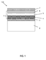
- FIG. 1 shows purely schematically an embodiment of a thin-film solar cell 100 according to the invention with a layer system 1 according to the invention in a cross-sectional view.
- the thin-film solar cell 100 comprises a substrate 2 and a back electrode 3.
- the layer system 1 according to the invention is arranged on the back electrode 3.
- the layer system 1 according to the invention comprises an absorber layer 4, a first buffer layer 5 and optionally a second buffer layer 6.
- a front electrode 7 is arranged on the layer system 1.
- the substrate 2 consists, for example, of inorganic glass, wherein equally other insulating materials with sufficient strength, as well as inert behavior with respect to the process steps carried out in the production of the thin-film solar cell 100 can be used, for example plastics, in particular polymers or metals, in particular metal alloys.
- the substrate 2 may be designed as a rigid plate or flexible film.
- the layer thickness of the substrate 2 is, for example, 1 mm to 5 mm.
- the return electrode 3 consists for example of an opaque metal. It can be deposited on the substrate 2, for example, by vapor deposition or magnetic field-assisted sputtering.
- the back electrode 3 consists for example of molybdenum (Mo), aluminum (Al), copper (Cu), titanium (Ti) or a multilayer system with such a metal, for example molybdenum (Mo).
- the layer thickness of the back electrode 3 here is less than 1 .mu.m, is preferably in the range of 300 nm to 600 nm and is for example 500 nm.
- the back electrode 3 serves as a rear side contact of the thin-film solar cell 100. Between the substrate 2 and the back electrode 3 can be an alkali metal. Barrier, which consists for example of Si 3 N 4 , SiON or SiCN. This is in FIG. 1 not shown in detail.
- the layer system 1 contains an absorber layer 4, for example of Cu (In, Ga) (S, Se) 2 , which is applied directly to the back electrode 3.
- the absorber layer 4 was deposited, for example, with the RTP process described above and has, for example, a thickness of 1.5 ⁇ m.
- the first buffer layer 5 contains a semiconductor material of the formula K x In y S z or Cs x In y S z with 0.05 ⁇ x / (x + y + z) ⁇ 0.25 and 0.30 ⁇ y / (y + z) ⁇ 0.45, preferably 0.05 ⁇ x / (x + y + z) ⁇ 0.20 and 0.35 ⁇ y / (y + z) ⁇ 0.45.
- K x In y S z it is preferable that 0.05 ⁇ x / (x + y + z) ⁇ 0.15 and 0.35 ⁇ y / (y + z) ⁇ 0.45.
- Cs x In y S z it is preferable that 0.05 ⁇ x / (x + y + z) ⁇ 0.12 and 0.35 ⁇ y / (y + z) ⁇ 0.45.
- the first buffer layer 5 besides a halogen, if potassium or cesium were deposited in a halogen compound, advantageously does not have a significant proportion ( ⁇ 1 atom%) of other elements.
- the layer thickness of the buffer layer 5 is preferably in the range of 15 nm to 60 nm and is for example 30 nm.
- the second buffer layer 6 is arranged.
- the second buffer layer 6 is optional, i. it does not necessarily have to be present in layer system 1.
- the buffer layer 6 contains, for example, undoped zinc oxide (i-ZnO).
- the front electrode 7 is arranged, which serves as a front side contact and transparent to radiation in the visible spectral range is ("window layer”).
- a doped metal oxide (TCO Transparent Conductive Oxide) is used for the front electrode 7, for example n-type, aluminum (Al) -doped zinc oxide (ZnO), boron (B) -doped zinc oxide (ZnO), or gallium ( Ga) -doped zinc oxide (ZnO).
- the layer thickness of the front electrode 7 is, for example, about 300 to 2000 nm.
- a plastic layer (encapsulation film) consisting of polyvinyl butyral (PVB), ethylene vinyl acetate (EVA) or DNP, for example, may be applied to the front electrode 7.
- cover plate which is transparent to sunlight and consists, for example, of extra-white glass (front glass) with a low iron content and has a thickness of, for example, 1 to 4 mm.
- the layer system 1 can likewise have a superstrate configuration in which the substrate 2 is transparent and the front electrode 7 is arranged on a surface of the substrate 2 facing away from the light entry side.
- the layer system 1 can be used to produce integrated series-connected thin film solar cells 100, wherein the layer system 1, the back electrode 3 and the front electrode 7 in a conventional manner by different structuring lines ("P1" for back electrode, "P2” for contact front electrode / back electrode and "P3 "for separation of the front electrode) is structured.
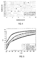
- FIG. 10 is a graph showing the efficiency of thin film solar cells 100 according to the structure of FIG. 1 as a function of the potassium content in the first buffer layer 5, which has a semiconductor material of the formula K x In y S z .
- the thin film solar cell 100 includes a substrate 2 of glass and a back electrode 3 of a Si 3 N 4 barrier layer and a molybdenum layer. On the back electrode 3, an absorber layer 4 made of Cu (In, Ga) (S, Se) 2 is deposited, which was deposited by the above-described RTP process. On the absorber layer 4, the first buffer layer 5 is arranged. The layer thickness of the first buffer layer 5 is 30 nm.
- a 100 nm thick second buffer layer 6 is arranged, which contains undoped zinc oxide.
- a 1200 nm thick front electrode 7 is arranged, which contains n-type zinc oxide.
- the area of the thin-film solar cell 100 is, for example, 1.4 cm 2 .
- Indium and sulfur are present in the first buffer layer 5 in the following molar ratio: 0.394 ⁇ y / (y + z) ⁇ 0.421.
- the potassium content of the first buffer layer 5 varies from 0 at% to 16 at%. The measurements showed a maximum efficiency of about 12.5%, whereby it can be seen that the efficiency is well above the efficiency (about 9%) of a comparable solar cell without potassium in the first buffer layer 5.
- FIG. 3 is a graph showing the efficiency of thin film solar cells 100 according to the structure of FIG. 1 as a function of the cesium content in the first buffer layer 5, which has a semiconductor material of the formula Cs x In y S z .
- the solar cells of the construction of FIG. 3 correspond to those of FIG. 2 with the exception that the indium sulfide-containing semiconductor material of the first buffer layer 5 was provided with cesium.
- indium and sulfur are present in the first buffer layer 5 in the following molar ratio: 0.400 ⁇ y / (y + z) ⁇ 0.413.
- the cesium content of the first buffer layer 5 varies from about 1.5 atomic% to about 14 atomic%.
- the measurements showed a maximum efficiency of about 16%, the efficiency is up to a cesium content of about 8 at% significantly above 14% and decreases from a cesium content of about 10 atomic%.
- FIG. 4 shows a measurement of the optical band gap Eg in electron volts (eV) as a function of the potassium content of K x In y Sz (: Cl) buffer layers produced by co-vapor deposition of KCl and InS.
- the optical band gap Eg is shown as a function of the sodium content of Na x In y Sz (: Cl) buffer layers produced by co-vapor deposition of NaCl and InS.
- the ratio y / (y + z) was about 0.39 to 0.42.
- the band gap was determined by ellipsometry, the potassium content determined by means of X-ray fluorescence analysis (RFA) on the chlorine content.
- RFA X-ray fluorescence analysis
- the band gap increases approximately linearly from about 2 eV to almost 2.5 eV at a potassium content in the range from 0 to 10.5 atom%, which leads to a corresponding increase in the short circuit current in a thin-film solar cell due to the reduced absorption .
- the band gaps of the Na-containing indium sulfide buffer layers are significantly lower than those of the K-containing indium sulfide buffer layers.
- FIG. 5 shows a measurement of the optical transmission of Cs x In y S z buffer layers on glass as a function of the cesium content.
- the respective cesium content in the buffer layer is shown in the diagram, with the lowest curve referring to a cesium-free indium sulfide buffer layer as a reference measurement.
- Fig. 6 shows a comparison of the efficiencies of thin film solar modules with In y S z : CsCl buffer layer (left) and In y S z : NaCl buffer layer (right). Obviously, significantly higher efficiencies can be achieved with a buffer layer containing a cesium-containing indium sulfide semiconductor material than with a buffer layer containing a sodium-containing indium sulfide semiconductor material.
- Fig. 7 the corresponding short-circuit current Isc (mA / cm 2 ) is shown. It can be seen a significant increase in the short-circuit current for solar modules with a buffer layer with a cesium-containing indium sulfide semiconductor material over a buffer layer with a sodium-containing indium sulfide semiconductor material. The introduction of CsCl in the buffer layer thus improves the transmission.
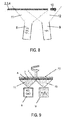
- the substrate 2 with back electrode 3 and absorber layer 4 is guided past the vapor lobes 11, 12 of a potassium or cesium source 8 and an indium sulfide source 9.
- the transport direction is indicated by an arrow with the reference numeral 10.
- the vapor lobes 11, 12 of the two sources 8, 9 partially overlap.
- potassium or cesium compounds and indium sulfide As starting materials for the production of a semiconductor material of the formula K x In y S z or Cs x In y S z it is possible to use potassium or cesium compounds and indium sulfide.
- compounds of potassium or cesium with the chalcogen sulfur, in particular K 2 S or Cs 2 S can be used.
- halide salts of potassium or cesium may be used, for example potassium fluoride (KF) or cesium fluoride (CsF), potassium chloride (KCl) or cesium chloride (CsCl), or corresponding bromides or iodides. This offers in particular by the easier handling of this relatively non-hazardous materials in a production environment advantages.
- the absorber layer 4 is coated with thin layers of a halogen or sulfide of potassium or cesium and indium sulfide, which mix.
- the two sources 8, 9 are, for example, effusion cells, from which the respective substance is thermally evaporated.
- any other form of production of steam lobes 11, 12 for the deposition of the buffer layer 5 is suitable, provided that the claimed ratio of the molar proportions of potassium or cesium and indium and sulfur can be adjusted.
- Alternative sources are, for example, small vessels of linear evaporators or crucibles of electron beam evaporators.
- the potassium or cesium compound is deposited on the absorber layer 4 in time before the indium sulfide, electrical passivation of the interface can be achieved, which improves the efficiency of the solar cell.
- FIG. 9 shows a further alternative embodiment of the method according to the invention using the example of a rotation method.
- the substrate 2 with back electrode 3 and absorber layer 4 is arranged on a rotatable sample carrier 13, for example on a sample carousel.
- Below the sample carrier 13 are alternately arranged sources of potassium or cesium 8 and indium sulfide 9.
- the sample carrier 13 is rotated. As a result, the substrate 2 in the vapor lobes 11, 12 is moved and coated.
- the evaporation rates of the sources 8,9 can be chosen so that the proportion of potassium and / or cesium varies so that a potassium and / or cesium gradient can be generated in the buffer layer 5.
- the optical band gap of the indium sulfide buffer layer can be widened.
- better band matching, reduced light absorption, as well as a significant increase in the short-circuit current and improved transmission, as well as overall higher efficiency can be achieved.
- the manufacturing process is inexpensive, effective and environmentally friendly.
Priority Applications (9)
| Application Number | Priority Date | Filing Date | Title |
|---|---|---|---|
| EP13199305.7A EP2887405A1 (de) | 2013-12-23 | 2013-12-23 | Schichtsystem für Dünnschichtsolarzellen |
| EP14874607.6A EP3087615B1 (en) | 2013-12-23 | 2014-12-23 | Layer system for thin-film solar cells |
| CN202010354738.3A CN111490117B (zh) | 2013-12-23 | 2014-12-23 | 用于薄膜太阳能电池的层系统 |
| KR1020167016720A KR101882595B1 (ko) | 2013-12-23 | 2014-12-23 | 박막 태양 전지를 위한 층 시스템 |
| PCT/CN2014/094607 WO2015096689A1 (en) | 2013-12-23 | 2014-12-23 | Layer System for Thin-Film Solar Cells |
| JP2016539927A JP6510529B2 (ja) | 2013-12-23 | 2014-12-23 | 薄膜太陽電池、薄膜太陽電池用層系及び薄膜太陽電池用層系の製造方法 |
| US15/107,085 US20170033245A1 (en) | 2013-12-23 | 2014-12-23 | Layer system for thin-film solar cells |
| ES14874607T ES2765496T3 (es) | 2013-12-23 | 2014-12-23 | Sistema de capas para células solares de película delgada |
| CN201480070532.0A CN106716646B (zh) | 2013-12-23 | 2014-12-23 | 用于薄膜太阳能电池的层系统 |
Applications Claiming Priority (1)
| Application Number | Priority Date | Filing Date | Title |
|---|---|---|---|
| EP13199305.7A EP2887405A1 (de) | 2013-12-23 | 2013-12-23 | Schichtsystem für Dünnschichtsolarzellen |
Publications (1)
| Publication Number | Publication Date |
|---|---|
| EP2887405A1 true EP2887405A1 (de) | 2015-06-24 |
Family
ID=49882918
Family Applications (2)
| Application Number | Title | Priority Date | Filing Date |
|---|---|---|---|
| EP13199305.7A Withdrawn EP2887405A1 (de) | 2013-12-23 | 2013-12-23 | Schichtsystem für Dünnschichtsolarzellen |
| EP14874607.6A Active EP3087615B1 (en) | 2013-12-23 | 2014-12-23 | Layer system for thin-film solar cells |
Family Applications After (1)
| Application Number | Title | Priority Date | Filing Date |
|---|---|---|---|
| EP14874607.6A Active EP3087615B1 (en) | 2013-12-23 | 2014-12-23 | Layer system for thin-film solar cells |
Country Status (7)
| Country | Link |
|---|---|
| US (1) | US20170033245A1 (zh) |
| EP (2) | EP2887405A1 (zh) |
| JP (1) | JP6510529B2 (zh) |
| KR (1) | KR101882595B1 (zh) |
| CN (2) | CN111490117B (zh) |
| ES (1) | ES2765496T3 (zh) |
| WO (1) | WO2015096689A1 (zh) |
Families Citing this family (3)
| Publication number | Priority date | Publication date | Assignee | Title |
|---|---|---|---|---|
| US11183605B2 (en) * | 2017-04-19 | 2021-11-23 | (Cnbm) Bengbu Design Research Institute For Glass Industry Co. Ltd | Method for producing a layer structure for thin-film solar cells using etching or laser ablation to produce rear-electrode-layer-free region |
| US10278258B2 (en) * | 2017-05-19 | 2019-04-30 | Panasonic Intellectual Property Management Co., Ltd. | Lighting device, luminaire, and signboard |
| JP2019087745A (ja) * | 2017-11-08 | 2019-06-06 | 東京応化工業株式会社 | 均一系塗布液及びその製造方法 |
Citations (5)
| Publication number | Priority date | Publication date | Assignee | Title |
|---|---|---|---|---|
| EP1356528A1 (fr) | 2001-01-31 | 2003-10-29 | Saint-Gobain Glass France | Sustrat transparent muni d'une electrode |
| DE19956735B4 (de) | 1999-11-25 | 2008-08-21 | Shell Erneuerbare Energien Gmbh | Dünnfilmsolarzelle mit einer Chalkopyritverbindung und einer Titan und Sauerstoff enthaltenden Verbindung |
| WO2009141132A2 (de) | 2008-05-19 | 2009-11-26 | Avancis Gmbh & Co. Kg | Schichtsystem für solarzellen |
| EP2200097A1 (en) * | 2008-12-16 | 2010-06-23 | Saint-Gobain Glass France S.A. | Method of manufacturing a photovoltaic device and system for patterning an object |
| US20120103411A1 (en) * | 2010-10-29 | 2012-05-03 | Pedro Gonzalez | Photovoltaic module substrate |
Family Cites Families (20)
| Publication number | Priority date | Publication date | Assignee | Title |
|---|---|---|---|---|
| US5252140A (en) * | 1987-07-24 | 1993-10-12 | Shigeyoshi Kobayashi | Solar cell substrate and process for its production |
| JPH10125941A (ja) * | 1996-10-23 | 1998-05-15 | Asahi Chem Ind Co Ltd | カルコパイライト型太陽電池 |
| JPH11204810A (ja) * | 1998-01-08 | 1999-07-30 | Asahi Chem Ind Co Ltd | 化合物半導体太陽電池 |
| CN1952222A (zh) * | 2005-10-20 | 2007-04-25 | 中国科学院福建物质结构研究所 | 含碱金属、镓或铟的硫属化合物晶体的生长方法 |
| JP4439492B2 (ja) * | 2006-05-25 | 2010-03-24 | 本田技研工業株式会社 | カルコパイライト型太陽電池およびその製造方法 |
| JP2008042611A (ja) * | 2006-08-08 | 2008-02-21 | Konica Minolta Medical & Graphic Inc | 超音波探触子の製造方法 |
| CN101092427A (zh) * | 2007-07-25 | 2007-12-26 | 哈尔滨工业大学 | 一种在水相中制备双-[γ-(三乙氧基硅)丙基]-四硫化物的方法 |
| EP3333280A1 (en) * | 2007-09-12 | 2018-06-13 | Flisom AG | Method for manufacturing a compound film with compositional grading |
| CN101299446A (zh) * | 2008-05-30 | 2008-11-05 | 南开大学 | 硒化物前驱薄膜与快速硒硫化热处理制备薄膜电池方法 |
| JP2010232608A (ja) * | 2009-03-30 | 2010-10-14 | Honda Motor Co Ltd | カルコパイライト型太陽電池の製造方法 |
| CN102130202A (zh) * | 2010-01-14 | 2011-07-20 | 正峰新能源股份有限公司 | 非真空形成铜铟镓硫硒吸收层及硫化镉缓冲层的方法及系统 |
| EP2360289A1 (de) * | 2010-02-23 | 2011-08-24 | Saint-Gobain Glass France | Vorrichtung und Verfahren zum Abscheiden einer aus mindestens zwei Komponenten bestehenden Schicht auf einem Gegenstand |
| JP2012059855A (ja) * | 2010-09-08 | 2012-03-22 | Nisshin Steel Co Ltd | Cigs太陽電池用基板および電池 |
| AU2011302008A1 (en) * | 2010-09-15 | 2013-05-09 | Precursor Energetics, Inc. | Deposition processes and devices for photovoltaics |
| CN102169910B (zh) * | 2011-01-14 | 2013-06-05 | 南开大学 | 一种基于硫属化合物纳米晶的薄膜太阳能电池 |
| JP2012174759A (ja) * | 2011-02-18 | 2012-09-10 | Fujifilm Corp | 化合物半導体層の製造方法および光電変換素子 |
| JP2012204617A (ja) * | 2011-03-25 | 2012-10-22 | Idemitsu Kosan Co Ltd | 光起電力素子、及び当該光起電力素子の製造方法 |
| JP5792008B2 (ja) * | 2011-09-14 | 2015-10-07 | 本田技研工業株式会社 | カルコパイライト型太陽電池の製造方法 |
| JP5174230B1 (ja) * | 2011-11-25 | 2013-04-03 | 昭和シェル石油株式会社 | 薄膜太陽電池モジュール及びその製造方法 |
| WO2013129557A1 (ja) * | 2012-03-02 | 2013-09-06 | Tdk株式会社 | 化合物半導体太陽電池及び化合物半導体太陽電池の光吸収層の製造方法 |
-
2013
- 2013-12-23 EP EP13199305.7A patent/EP2887405A1/de not_active Withdrawn
-
2014
- 2014-12-23 CN CN202010354738.3A patent/CN111490117B/zh active Active
- 2014-12-23 CN CN201480070532.0A patent/CN106716646B/zh active Active
- 2014-12-23 JP JP2016539927A patent/JP6510529B2/ja active Active
- 2014-12-23 ES ES14874607T patent/ES2765496T3/es active Active
- 2014-12-23 KR KR1020167016720A patent/KR101882595B1/ko active IP Right Grant
- 2014-12-23 EP EP14874607.6A patent/EP3087615B1/en active Active
- 2014-12-23 WO PCT/CN2014/094607 patent/WO2015096689A1/en active Application Filing
- 2014-12-23 US US15/107,085 patent/US20170033245A1/en not_active Abandoned
Patent Citations (5)
| Publication number | Priority date | Publication date | Assignee | Title |
|---|---|---|---|---|
| DE19956735B4 (de) | 1999-11-25 | 2008-08-21 | Shell Erneuerbare Energien Gmbh | Dünnfilmsolarzelle mit einer Chalkopyritverbindung und einer Titan und Sauerstoff enthaltenden Verbindung |
| EP1356528A1 (fr) | 2001-01-31 | 2003-10-29 | Saint-Gobain Glass France | Sustrat transparent muni d'une electrode |
| WO2009141132A2 (de) | 2008-05-19 | 2009-11-26 | Avancis Gmbh & Co. Kg | Schichtsystem für solarzellen |
| EP2200097A1 (en) * | 2008-12-16 | 2010-06-23 | Saint-Gobain Glass France S.A. | Method of manufacturing a photovoltaic device and system for patterning an object |
| US20120103411A1 (en) * | 2010-10-29 | 2012-05-03 | Pedro Gonzalez | Photovoltaic module substrate |
Non-Patent Citations (1)
| Title |
|---|
| RODRIGO SÁEZ-ARAOZ ET AL: "ILGAR In2S3 buffer layers for Cd-free Cu(In,Ga)(S,Se)2 solar cells with certified efficiencies above 16%", PROGRESS IN PHOTOVOLTAICS: RESEARCH AND APPLICATIONS, 1 July 2012 (2012-07-01), pages n/a - n/a, XP055041070, ISSN: 1062-7995, DOI: 10.1002/pip.2268 * |
Also Published As
| Publication number | Publication date |
|---|---|
| KR20160137947A (ko) | 2016-12-02 |
| CN106716646A (zh) | 2017-05-24 |
| EP3087615A1 (en) | 2016-11-02 |
| ES2765496T3 (es) | 2020-06-09 |
| US20170033245A1 (en) | 2017-02-02 |
| EP3087615A4 (en) | 2017-09-27 |
| KR101882595B1 (ko) | 2018-08-24 |
| CN111490117A (zh) | 2020-08-04 |
| JP2016541124A (ja) | 2016-12-28 |
| EP3087615B1 (en) | 2019-10-09 |
| WO2015096689A1 (en) | 2015-07-02 |
| CN111490117B (zh) | 2022-03-11 |
| CN106716646B (zh) | 2020-06-09 |
| JP6510529B2 (ja) | 2019-05-08 |
Similar Documents
| Publication | Publication Date | Title |
|---|---|---|
| EP2281310B1 (de) | Schichtsystem für solarzellen | |
| DE112012003297B4 (de) | Deckschichten für verbesserte Kristallisation | |
| EP2684212A1 (de) | Verfahren zur herstellung des pentanären verbindungshalbleiters cztsse, sowie dünnschichtsolarzelle | |
| DE112015000755T5 (de) | Dünnfilm-Solarzelle auf Verbindungsbasis | |
| EP2887405A1 (de) | Schichtsystem für Dünnschichtsolarzellen | |
| EP2865011B1 (de) | Schichtsystem für dünnschicht-solarzellen mit einer naxinisyclz-pufferschicht | |
| EP3014652B1 (de) | Schichtsystem für dünnschichtsolarzellen mit natriumindiumsulfid-pufferschicht | |
| EP2865001B1 (de) | Schichtsystem für dünnschichtsolarzellen | |
| EP2865012B1 (de) | Schichtsystem für dünnschichtsolarzellen | |
| DE102014223485A1 (de) | Schichtaufbau für eine Dünnschichtsolarzelle und Herstellungsverfahren | |
| EP3238228B1 (en) | Method for producing a layer system for thin-film solar cells having a sodium indium sulfide buffer layer | |
| DE102010004359B4 (de) | Optoelektronisches Funktionsmaterial, seine Herstellung und Verwendung | |
| EP3627564A1 (de) | Verfahren zur nachbehandlung einer absorberschicht | |
| WO2014207233A1 (de) | Schichtsystem für dünnschichtsolarzellen mit indiumsulfid-pufferschicht | |
| EP2936548A1 (de) | Verfahren zur herstellung eines verbindungshalbleiters sowie dünnschichtsolarzelle | |
| DE202015106923U1 (de) | Elektronisch leitfähiges Substrat für Photovoltaikzellen |
Legal Events
| Date | Code | Title | Description |
|---|---|---|---|
| PUAI | Public reference made under article 153(3) epc to a published international application that has entered the european phase |
Free format text: ORIGINAL CODE: 0009012 |
|
| 17P | Request for examination filed |
Effective date: 20131223 |
|
| AK | Designated contracting states |
Kind code of ref document: A1 Designated state(s): AL AT BE BG CH CY CZ DE DK EE ES FI FR GB GR HR HU IE IS IT LI LT LU LV MC MK MT NL NO PL PT RO RS SE SI SK SM TR |
|
| AX | Request for extension of the european patent |
Extension state: BA ME |
|
| STAA | Information on the status of an ep patent application or granted ep patent |
Free format text: STATUS: THE APPLICATION HAS BEEN WITHDRAWN |
|
| 18W | Application withdrawn |
Effective date: 20151015 |