EP2873103B1 - Piezoelectric material and piezoelectric element using the same, and electronic apparatus using the piezoelectronic element - Google Patents
Piezoelectric material and piezoelectric element using the same, and electronic apparatus using the piezoelectronic element Download PDFInfo
- Publication number
- EP2873103B1 EP2873103B1 EP13760118.3A EP13760118A EP2873103B1 EP 2873103 B1 EP2873103 B1 EP 2873103B1 EP 13760118 A EP13760118 A EP 13760118A EP 2873103 B1 EP2873103 B1 EP 2873103B1
- Authority
- EP
- European Patent Office
- Prior art keywords
- piezoelectric element
- piezoelectric
- electrode
- piezoelectric material
- multilayered
- Prior art date
- Legal status (The legal status is an assumption and is not a legal conclusion. Google has not performed a legal analysis and makes no representation as to the accuracy of the status listed.)
- Active
Links
- 239000000463 material Substances 0.000 title claims description 157
- 239000007788 liquid Substances 0.000 claims description 68
- 239000000843 powder Substances 0.000 claims description 53
- 239000000203 mixture Substances 0.000 claims description 41
- 239000000428 dust Substances 0.000 claims description 40
- 230000003287 optical effect Effects 0.000 claims description 34
- 238000005245 sintering Methods 0.000 claims description 32
- 238000003384 imaging method Methods 0.000 claims description 30
- 229910044991 metal oxide Inorganic materials 0.000 claims description 28
- 150000004706 metal oxides Chemical class 0.000 claims description 28
- 229910052802 copper Inorganic materials 0.000 claims description 19
- 238000004519 manufacturing process Methods 0.000 claims description 15
- 239000002002 slurry Substances 0.000 claims description 14
- 229910052719 titanium Inorganic materials 0.000 claims description 13
- 229910052700 potassium Inorganic materials 0.000 claims description 12
- 150000002736 metal compounds Chemical class 0.000 claims description 9
- 229910052763 palladium Inorganic materials 0.000 claims description 8
- 229910052709 silver Inorganic materials 0.000 claims description 8
- 229910052759 nickel Inorganic materials 0.000 claims description 6
- 239000010949 copper Substances 0.000 description 40
- 238000000034 method Methods 0.000 description 35
- 239000010955 niobium Substances 0.000 description 28
- 230000000052 comparative effect Effects 0.000 description 27
- 229910002113 barium titanate Inorganic materials 0.000 description 25
- 239000010936 titanium Substances 0.000 description 25
- 239000011734 sodium Substances 0.000 description 24
- 239000012071 phase Substances 0.000 description 22
- 229910052751 metal Inorganic materials 0.000 description 19
- UYLYBEXRJGPQSH-UHFFFAOYSA-N sodium;oxido(dioxo)niobium Chemical compound [Na+].[O-][Nb](=O)=O UYLYBEXRJGPQSH-UHFFFAOYSA-N 0.000 description 19
- JRPBQTZRNDNNOP-UHFFFAOYSA-N barium titanate Chemical compound [Ba+2].[Ba+2].[O-][Ti]([O-])([O-])[O-] JRPBQTZRNDNNOP-UHFFFAOYSA-N 0.000 description 18
- 230000010287 polarization Effects 0.000 description 18
- 239000002994 raw material Substances 0.000 description 17
- QPLDLSVMHZLSFG-UHFFFAOYSA-N Copper oxide Chemical compound [Cu]=O QPLDLSVMHZLSFG-UHFFFAOYSA-N 0.000 description 16
- 150000001875 compounds Chemical class 0.000 description 16
- 239000011230 binding agent Substances 0.000 description 15
- 239000002184 metal Substances 0.000 description 15
- 238000010304 firing Methods 0.000 description 14
- 229910010252 TiO3 Inorganic materials 0.000 description 12
- 238000009413 insulation Methods 0.000 description 12
- YPQJHZKJHIBJAP-UHFFFAOYSA-N [K].[Bi] Chemical compound [K].[Bi] YPQJHZKJHIBJAP-UHFFFAOYSA-N 0.000 description 11
- 229910052797 bismuth Inorganic materials 0.000 description 10
- PXHVJJICTQNCMI-UHFFFAOYSA-N nickel Substances [Ni] PXHVJJICTQNCMI-UHFFFAOYSA-N 0.000 description 10
- 229910052758 niobium Inorganic materials 0.000 description 10
- 238000002441 X-ray diffraction Methods 0.000 description 9
- 229910052788 barium Inorganic materials 0.000 description 9
- 230000005540 biological transmission Effects 0.000 description 9
- 239000013078 crystal Substances 0.000 description 9
- 230000010355 oscillation Effects 0.000 description 9
- 239000000919 ceramic Substances 0.000 description 8
- 229910052708 sodium Inorganic materials 0.000 description 8
- 238000004544 sputter deposition Methods 0.000 description 8
- 229910003378 NaNbO3 Inorganic materials 0.000 description 7
- 230000007423 decrease Effects 0.000 description 7
- 238000010586 diagram Methods 0.000 description 7
- 239000010931 gold Substances 0.000 description 7
- 238000010438 heat treatment Methods 0.000 description 7
- 238000002156 mixing Methods 0.000 description 7
- 229920002037 poly(vinyl butyral) polymer Polymers 0.000 description 7
- MUPJWXCPTRQOKY-UHFFFAOYSA-N sodium;niobium(5+);oxygen(2-) Chemical compound [O-2].[O-2].[O-2].[Na+].[Nb+5] MUPJWXCPTRQOKY-UHFFFAOYSA-N 0.000 description 7
- DGAQECJNVWCQMB-PUAWFVPOSA-M Ilexoside XXIX Chemical compound C[C@@H]1CC[C@@]2(CC[C@@]3(C(=CC[C@H]4[C@]3(CC[C@@H]5[C@@]4(CC[C@@H](C5(C)C)OS(=O)(=O)[O-])C)C)[C@@H]2[C@]1(C)O)C)C(=O)O[C@H]6[C@@H]([C@H]([C@@H]([C@H](O6)CO)O)O)O.[Na+] DGAQECJNVWCQMB-PUAWFVPOSA-M 0.000 description 6
- RTAQQCXQSZGOHL-UHFFFAOYSA-N Titanium Chemical compound [Ti] RTAQQCXQSZGOHL-UHFFFAOYSA-N 0.000 description 6
- YXFVVABEGXRONW-UHFFFAOYSA-N Toluene Chemical compound CC1=CC=CC=C1 YXFVVABEGXRONW-UHFFFAOYSA-N 0.000 description 6
- 239000000956 alloy Substances 0.000 description 6
- 229910045601 alloy Inorganic materials 0.000 description 6
- DSAJWYNOEDNPEQ-UHFFFAOYSA-N barium atom Chemical compound [Ba] DSAJWYNOEDNPEQ-UHFFFAOYSA-N 0.000 description 6
- DOIRQSBPFJWKBE-UHFFFAOYSA-N dibutyl phthalate Chemical compound CCCCOC(=O)C1=CC=CC=C1C(=O)OCCCC DOIRQSBPFJWKBE-UHFFFAOYSA-N 0.000 description 6
- 239000007772 electrode material Substances 0.000 description 6
- GUCVJGMIXFAOAE-UHFFFAOYSA-N niobium atom Chemical compound [Nb] GUCVJGMIXFAOAE-UHFFFAOYSA-N 0.000 description 6
- 238000007650 screen-printing Methods 0.000 description 6
- LFQSCWFLJHTTHZ-UHFFFAOYSA-N Ethanol Chemical compound CCO LFQSCWFLJHTTHZ-UHFFFAOYSA-N 0.000 description 5
- 238000007906 compression Methods 0.000 description 5
- 230000006835 compression Effects 0.000 description 5
- 238000007606 doctor blade method Methods 0.000 description 5
- 238000001035 drying Methods 0.000 description 5
- 229910052737 gold Inorganic materials 0.000 description 5
- 238000009616 inductively coupled plasma Methods 0.000 description 5
- 229910052760 oxygen Inorganic materials 0.000 description 5
- NRNCYVBFPDDJNE-UHFFFAOYSA-N pemoline Chemical compound O1C(N)=NC(=O)C1C1=CC=CC=C1 NRNCYVBFPDDJNE-UHFFFAOYSA-N 0.000 description 5
- 230000011514 reflex Effects 0.000 description 5
- 239000000758 substrate Substances 0.000 description 5
- RYGMFSIKBFXOCR-UHFFFAOYSA-N Copper Chemical compound [Cu] RYGMFSIKBFXOCR-UHFFFAOYSA-N 0.000 description 4
- 239000005751 Copper oxide Substances 0.000 description 4
- 239000004372 Polyvinyl alcohol Substances 0.000 description 4
- ZLMJMSJWJFRBEC-UHFFFAOYSA-N Potassium Chemical group [K] ZLMJMSJWJFRBEC-UHFFFAOYSA-N 0.000 description 4
- QVGXLLKOCUKJST-UHFFFAOYSA-N atomic oxygen Chemical compound [O] QVGXLLKOCUKJST-UHFFFAOYSA-N 0.000 description 4
- JCXGWMGPZLAOME-UHFFFAOYSA-N bismuth atom Chemical compound [Bi] JCXGWMGPZLAOME-UHFFFAOYSA-N 0.000 description 4
- 238000000224 chemical solution deposition Methods 0.000 description 4
- 229910017052 cobalt Inorganic materials 0.000 description 4
- 239000010941 cobalt Substances 0.000 description 4
- GUTLYIVDDKVIGB-UHFFFAOYSA-N cobalt atom Chemical compound [Co] GUTLYIVDDKVIGB-UHFFFAOYSA-N 0.000 description 4
- 229910000431 copper oxide Inorganic materials 0.000 description 4
- BERDEBHAJNAUOM-UHFFFAOYSA-N copper(i) oxide Chemical compound [Cu]O[Cu] BERDEBHAJNAUOM-UHFFFAOYSA-N 0.000 description 4
- 230000007547 defect Effects 0.000 description 4
- 238000011156 evaluation Methods 0.000 description 4
- 238000005469 granulation Methods 0.000 description 4
- 230000003179 granulation Effects 0.000 description 4
- 238000001513 hot isostatic pressing Methods 0.000 description 4
- 239000012535 impurity Substances 0.000 description 4
- 238000005304 joining Methods 0.000 description 4
- 239000001301 oxygen Substances 0.000 description 4
- 239000002245 particle Substances 0.000 description 4
- 239000004014 plasticizer Substances 0.000 description 4
- 229920002451 polyvinyl alcohol Polymers 0.000 description 4
- 239000011591 potassium Substances 0.000 description 4
- 238000003825 pressing Methods 0.000 description 4
- 239000002904 solvent Substances 0.000 description 4
- 239000000853 adhesive Substances 0.000 description 3
- 230000001070 adhesive effect Effects 0.000 description 3
- 230000008602 contraction Effects 0.000 description 3
- 230000000694 effects Effects 0.000 description 3
- 230000005684 electric field Effects 0.000 description 3
- 230000033001 locomotion Effects 0.000 description 3
- 238000002844 melting Methods 0.000 description 3
- 230000008018 melting Effects 0.000 description 3
- 239000011812 mixed powder Substances 0.000 description 3
- 230000002093 peripheral effect Effects 0.000 description 3
- 238000007639 printing Methods 0.000 description 3
- 238000011084 recovery Methods 0.000 description 3
- 229910052712 strontium Inorganic materials 0.000 description 3
- 239000000126 substance Substances 0.000 description 3
- 238000010897 surface acoustic wave method Methods 0.000 description 3
- 229910052715 tantalum Inorganic materials 0.000 description 3
- 239000004925 Acrylic resin Substances 0.000 description 2
- 229920000178 Acrylic resin Polymers 0.000 description 2
- 229920002799 BoPET Polymers 0.000 description 2
- CDBYLPFSWZWCQE-UHFFFAOYSA-L Sodium Carbonate Chemical compound [Na+].[Na+].[O-]C([O-])=O CDBYLPFSWZWCQE-UHFFFAOYSA-L 0.000 description 2
- 229910052782 aluminium Inorganic materials 0.000 description 2
- IWOUKMZUPDVPGQ-UHFFFAOYSA-N barium nitrate Chemical compound [Ba+2].[O-][N+]([O-])=O.[O-][N+]([O-])=O IWOUKMZUPDVPGQ-UHFFFAOYSA-N 0.000 description 2
- QVQLCTNNEUAWMS-UHFFFAOYSA-N barium oxide Chemical compound [Ba]=O QVQLCTNNEUAWMS-UHFFFAOYSA-N 0.000 description 2
- 229910021523 barium zirconate Inorganic materials 0.000 description 2
- DQBAOWPVHRWLJC-UHFFFAOYSA-N barium(2+);dioxido(oxo)zirconium Chemical compound [Ba+2].[O-][Zr]([O-])=O DQBAOWPVHRWLJC-UHFFFAOYSA-N 0.000 description 2
- 239000011324 bead Substances 0.000 description 2
- DKPFZGUDAPQIHT-UHFFFAOYSA-N butyl acetate Chemical compound CCCCOC(C)=O DKPFZGUDAPQIHT-UHFFFAOYSA-N 0.000 description 2
- 238000001354 calcination Methods 0.000 description 2
- 230000008859 change Effects 0.000 description 2
- 229910052804 chromium Inorganic materials 0.000 description 2
- 238000009694 cold isostatic pressing Methods 0.000 description 2
- OPQARKPSCNTWTJ-UHFFFAOYSA-L copper(ii) acetate Chemical compound [Cu+2].CC([O-])=O.CC([O-])=O OPQARKPSCNTWTJ-UHFFFAOYSA-L 0.000 description 2
- RKTYLMNFRDHKIL-UHFFFAOYSA-N copper;5,10,15,20-tetraphenylporphyrin-22,24-diide Chemical group [Cu+2].C1=CC(C(=C2C=CC([N-]2)=C(C=2C=CC=CC=2)C=2C=CC(N=2)=C(C=2C=CC=CC=2)C2=CC=C3[N-]2)C=2C=CC=CC=2)=NC1=C3C1=CC=CC=C1 RKTYLMNFRDHKIL-UHFFFAOYSA-N 0.000 description 2
- 230000003247 decreasing effect Effects 0.000 description 2
- 230000018044 dehydration Effects 0.000 description 2
- 238000006297 dehydration reaction Methods 0.000 description 2
- 238000000151 deposition Methods 0.000 description 2
- 230000008021 deposition Effects 0.000 description 2
- 238000006073 displacement reaction Methods 0.000 description 2
- 238000009826 distribution Methods 0.000 description 2
- 238000005516 engineering process Methods 0.000 description 2
- -1 for example Substances 0.000 description 2
- 230000006870 function Effects 0.000 description 2
- 239000007789 gas Substances 0.000 description 2
- 229910052738 indium Inorganic materials 0.000 description 2
- 229910052741 iridium Inorganic materials 0.000 description 2
- 229910052742 iron Inorganic materials 0.000 description 2
- 238000010030 laminating Methods 0.000 description 2
- 239000007791 liquid phase Substances 0.000 description 2
- 150000002739 metals Chemical class 0.000 description 2
- KDLHZDBZIXYQEI-UHFFFAOYSA-N palladium Substances [Pd] KDLHZDBZIXYQEI-UHFFFAOYSA-N 0.000 description 2
- 238000005192 partition Methods 0.000 description 2
- 229920003023 plastic Polymers 0.000 description 2
- 239000004033 plastic Substances 0.000 description 2
- 229910052697 platinum Inorganic materials 0.000 description 2
- 239000011148 porous material Substances 0.000 description 2
- BWHMMNNQKKPAPP-UHFFFAOYSA-L potassium carbonate Chemical compound [K+].[K+].[O-]C([O-])=O BWHMMNNQKKPAPP-UHFFFAOYSA-L 0.000 description 2
- FGIUAXJPYTZDNR-UHFFFAOYSA-N potassium nitrate Chemical compound [K+].[O-][N+]([O-])=O FGIUAXJPYTZDNR-UHFFFAOYSA-N 0.000 description 2
- 230000008569 process Effects 0.000 description 2
- 238000012545 processing Methods 0.000 description 2
- 239000000047 product Substances 0.000 description 2
- 230000002441 reversible effect Effects 0.000 description 2
- 239000010944 silver (metal) Substances 0.000 description 2
- 239000007787 solid Substances 0.000 description 2
- 230000002269 spontaneous effect Effects 0.000 description 2
- 229910052718 tin Inorganic materials 0.000 description 2
- OGIDPMRJRNCKJF-UHFFFAOYSA-N titanium oxide Inorganic materials [Ti]=O OGIDPMRJRNCKJF-UHFFFAOYSA-N 0.000 description 2
- 230000007704 transition Effects 0.000 description 2
- 238000003826 uniaxial pressing Methods 0.000 description 2
- 238000007740 vapor deposition Methods 0.000 description 2
- XLYOFNOQVPJJNP-UHFFFAOYSA-N water Substances O XLYOFNOQVPJJNP-UHFFFAOYSA-N 0.000 description 2
- 238000007088 Archimedes method Methods 0.000 description 1
- ZOXJGFHDIHLPTG-UHFFFAOYSA-N Boron Chemical compound [B] ZOXJGFHDIHLPTG-UHFFFAOYSA-N 0.000 description 1
- OYPRJOBELJOOCE-UHFFFAOYSA-N Calcium Chemical compound [Ca] OYPRJOBELJOOCE-UHFFFAOYSA-N 0.000 description 1
- OKTJSMMVPCPJKN-UHFFFAOYSA-N Carbon Chemical compound [C] OKTJSMMVPCPJKN-UHFFFAOYSA-N 0.000 description 1
- 229920001651 Cyanoacrylate Polymers 0.000 description 1
- MQIUGAXCHLFZKX-UHFFFAOYSA-N Di-n-octyl phthalate Natural products CCCCCCCCOC(=O)C1=CC=CC=C1C(=O)OCCCCCCCC MQIUGAXCHLFZKX-UHFFFAOYSA-N 0.000 description 1
- PXGOKWXKJXAPGV-UHFFFAOYSA-N Fluorine Chemical compound FF PXGOKWXKJXAPGV-UHFFFAOYSA-N 0.000 description 1
- MWCLLHOVUTZFKS-UHFFFAOYSA-N Methyl cyanoacrylate Chemical compound COC(=O)C(=C)C#N MWCLLHOVUTZFKS-UHFFFAOYSA-N 0.000 description 1
- OAICVXFJPJFONN-UHFFFAOYSA-N Phosphorus Chemical compound [P] OAICVXFJPJFONN-UHFFFAOYSA-N 0.000 description 1
- GWEVSGVZZGPLCZ-UHFFFAOYSA-N Titan oxide Chemical compound O=[Ti]=O GWEVSGVZZGPLCZ-UHFFFAOYSA-N 0.000 description 1
- 238000004430 X-ray Raman scattering Methods 0.000 description 1
- 238000000441 X-ray spectroscopy Methods 0.000 description 1
- 238000003916 acid precipitation Methods 0.000 description 1
- 230000002411 adverse Effects 0.000 description 1
- 239000000443 aerosol Substances 0.000 description 1
- 238000004458 analytical method Methods 0.000 description 1
- 150000001450 anions Chemical class 0.000 description 1
- ITHZDDVSAWDQPZ-UHFFFAOYSA-L barium acetate Chemical compound [Ba+2].CC([O-])=O.CC([O-])=O ITHZDDVSAWDQPZ-UHFFFAOYSA-L 0.000 description 1
- GXUARMXARIJAFV-UHFFFAOYSA-L barium oxalate Chemical compound [Ba+2].[O-]C(=O)C([O-])=O GXUARMXARIJAFV-UHFFFAOYSA-L 0.000 description 1
- 229940094800 barium oxalate Drugs 0.000 description 1
- AYJRCSIUFZENHW-DEQYMQKBSA-L barium(2+);oxomethanediolate Chemical compound [Ba+2].[O-][14C]([O-])=O AYJRCSIUFZENHW-DEQYMQKBSA-L 0.000 description 1
- 230000008901 benefit Effects 0.000 description 1
- BJQHLKABXJIVAM-UHFFFAOYSA-N bis(2-ethylhexyl) phthalate Chemical compound CCCCC(CC)COC(=O)C1=CC=CC=C1C(=O)OCC(CC)CCCC BJQHLKABXJIVAM-UHFFFAOYSA-N 0.000 description 1
- JHXKRIRFYBPWGE-UHFFFAOYSA-K bismuth chloride Chemical compound Cl[Bi](Cl)Cl JHXKRIRFYBPWGE-UHFFFAOYSA-K 0.000 description 1
- 229940049676 bismuth hydroxide Drugs 0.000 description 1
- 229910000416 bismuth oxide Inorganic materials 0.000 description 1
- 229940073609 bismuth oxychloride Drugs 0.000 description 1
- TXKAQZRUJUNDHI-UHFFFAOYSA-K bismuth tribromide Chemical compound Br[Bi](Br)Br TXKAQZRUJUNDHI-UHFFFAOYSA-K 0.000 description 1
- TZSXPYWRDWEXHG-UHFFFAOYSA-K bismuth;trihydroxide Chemical compound [OH-].[OH-].[OH-].[Bi+3] TZSXPYWRDWEXHG-UHFFFAOYSA-K 0.000 description 1
- 229910052796 boron Inorganic materials 0.000 description 1
- 229910052791 calcium Inorganic materials 0.000 description 1
- 239000011575 calcium Substances 0.000 description 1
- AOWKSNWVBZGMTJ-UHFFFAOYSA-N calcium titanate Chemical compound [Ca+2].[O-][Ti]([O-])=O AOWKSNWVBZGMTJ-UHFFFAOYSA-N 0.000 description 1
- 238000004364 calculation method Methods 0.000 description 1
- 239000003990 capacitor Substances 0.000 description 1
- 229910052799 carbon Inorganic materials 0.000 description 1
- 238000005229 chemical vapour deposition Methods 0.000 description 1
- 239000011248 coating agent Substances 0.000 description 1
- 238000000576 coating method Methods 0.000 description 1
- 239000004020 conductor Substances 0.000 description 1
- 229940116318 copper carbonate Drugs 0.000 description 1
- GEZOTWYUIKXWOA-UHFFFAOYSA-L copper;carbonate Chemical compound [Cu+2].[O-]C([O-])=O GEZOTWYUIKXWOA-UHFFFAOYSA-L 0.000 description 1
- QYCVHILLJSYYBD-UHFFFAOYSA-L copper;oxalate Chemical compound [Cu+2].[O-]C(=O)C([O-])=O QYCVHILLJSYYBD-UHFFFAOYSA-L 0.000 description 1
- 230000008878 coupling Effects 0.000 description 1
- 238000010168 coupling process Methods 0.000 description 1
- 238000005859 coupling reaction Methods 0.000 description 1
- 238000005520 cutting process Methods 0.000 description 1
- 230000002950 deficient Effects 0.000 description 1
- 230000006866 deterioration Effects 0.000 description 1
- 238000011161 development Methods 0.000 description 1
- 230000018109 developmental process Effects 0.000 description 1
- TYIXMATWDRGMPF-UHFFFAOYSA-N dibismuth;oxygen(2-) Chemical compound [O-2].[O-2].[O-2].[Bi+3].[Bi+3] TYIXMATWDRGMPF-UHFFFAOYSA-N 0.000 description 1
- 239000003989 dielectric material Substances 0.000 description 1
- MIMDHDXOBDPUQW-UHFFFAOYSA-N dioctyl decanedioate Chemical compound CCCCCCCCOC(=O)CCCCCCCCC(=O)OCCCCCCCC MIMDHDXOBDPUQW-UHFFFAOYSA-N 0.000 description 1
- 238000010894 electron beam technology Methods 0.000 description 1
- 238000001125 extrusion Methods 0.000 description 1
- 239000011737 fluorine Substances 0.000 description 1
- 229910052731 fluorine Inorganic materials 0.000 description 1
- 239000000446 fuel Substances 0.000 description 1
- 230000009477 glass transition Effects 0.000 description 1
- PCHJSUWPFVWCPO-UHFFFAOYSA-N gold Chemical compound [Au] PCHJSUWPFVWCPO-UHFFFAOYSA-N 0.000 description 1
- 231100001261 hazardous Toxicity 0.000 description 1
- 230000020169 heat generation Effects 0.000 description 1
- 238000007602 hot air drying Methods 0.000 description 1
- RXPAJWPEYBDXOG-UHFFFAOYSA-N hydron;methyl 4-methoxypyridine-2-carboxylate;chloride Chemical compound Cl.COC(=O)C1=CC(OC)=CC=N1 RXPAJWPEYBDXOG-UHFFFAOYSA-N 0.000 description 1
- 238000001027 hydrothermal synthesis Methods 0.000 description 1
- 238000002354 inductively-coupled plasma atomic emission spectroscopy Methods 0.000 description 1
- 239000000976 ink Substances 0.000 description 1
- 239000013067 intermediate product Substances 0.000 description 1
- 150000002500 ions Chemical class 0.000 description 1
- 229910052451 lead zirconate titanate Inorganic materials 0.000 description 1
- HFGPZNIAWCZYJU-UHFFFAOYSA-N lead zirconate titanate Chemical compound [O-2].[O-2].[O-2].[O-2].[O-2].[Ti+4].[Zr+4].[Pb+2] HFGPZNIAWCZYJU-UHFFFAOYSA-N 0.000 description 1
- 238000005259 measurement Methods 0.000 description 1
- 230000007246 mechanism Effects 0.000 description 1
- 230000028161 membrane depolarization Effects 0.000 description 1
- 238000009768 microwave sintering Methods 0.000 description 1
- 239000012046 mixed solvent Substances 0.000 description 1
- 229910000484 niobium oxide Inorganic materials 0.000 description 1
- URLJKFSTXLNXLG-UHFFFAOYSA-N niobium(5+);oxygen(2-) Chemical compound [O-2].[O-2].[O-2].[O-2].[O-2].[Nb+5].[Nb+5] URLJKFSTXLNXLG-UHFFFAOYSA-N 0.000 description 1
- ORQBXQOJMQIAOY-UHFFFAOYSA-N nobelium Chemical compound [No] ORQBXQOJMQIAOY-UHFFFAOYSA-N 0.000 description 1
- BWOROQSFKKODDR-UHFFFAOYSA-N oxobismuth;hydrochloride Chemical compound Cl.[Bi]=O BWOROQSFKKODDR-UHFFFAOYSA-N 0.000 description 1
- 229910052698 phosphorus Inorganic materials 0.000 description 1
- 239000011574 phosphorus Substances 0.000 description 1
- 230000000704 physical effect Effects 0.000 description 1
- 238000005498 polishing Methods 0.000 description 1
- 229910000027 potassium carbonate Inorganic materials 0.000 description 1
- 239000004323 potassium nitrate Substances 0.000 description 1
- 235000010333 potassium nitrate Nutrition 0.000 description 1
- 239000002243 precursor Substances 0.000 description 1
- 238000002360 preparation method Methods 0.000 description 1
- KCTAWXVAICEBSD-UHFFFAOYSA-N prop-2-enoyloxy prop-2-eneperoxoate Chemical compound C=CC(=O)OOOC(=O)C=C KCTAWXVAICEBSD-UHFFFAOYSA-N 0.000 description 1
- 230000009467 reduction Effects 0.000 description 1
- 238000012827 research and development Methods 0.000 description 1
- 238000007569 slipcasting Methods 0.000 description 1
- 229910000029 sodium carbonate Inorganic materials 0.000 description 1
- 239000002689 soil Substances 0.000 description 1
- 238000003980 solgel method Methods 0.000 description 1
- 239000006104 solid solution Substances 0.000 description 1
- 239000000243 solution Substances 0.000 description 1
- 238000001694 spray drying Methods 0.000 description 1
- 239000007858 starting material Substances 0.000 description 1
- CIOAGBVUUVVLOB-UHFFFAOYSA-N strontium atom Chemical compound [Sr] CIOAGBVUUVVLOB-UHFFFAOYSA-N 0.000 description 1
- GUVRBAGPIYLISA-UHFFFAOYSA-N tantalum atom Chemical compound [Ta] GUVRBAGPIYLISA-UHFFFAOYSA-N 0.000 description 1
- 239000012780 transparent material Substances 0.000 description 1
- 229910052720 vanadium Inorganic materials 0.000 description 1
- GPPXJZIENCGNKB-UHFFFAOYSA-N vanadium Chemical compound [V]#[V] GPPXJZIENCGNKB-UHFFFAOYSA-N 0.000 description 1
- 239000012856 weighed raw material Substances 0.000 description 1
- 238000005303 weighing Methods 0.000 description 1
- 229910052726 zirconium Inorganic materials 0.000 description 1
Images


Classifications
-
- H—ELECTRICITY
- H10—SEMICONDUCTOR DEVICES; ELECTRIC SOLID-STATE DEVICES NOT OTHERWISE PROVIDED FOR
- H10N—ELECTRIC SOLID-STATE DEVICES NOT OTHERWISE PROVIDED FOR
- H10N30/00—Piezoelectric or electrostrictive devices
- H10N30/80—Constructional details
- H10N30/85—Piezoelectric or electrostrictive active materials
- H10N30/852—Composite materials, e.g. having 1-3 or 2-2 type connectivity
-
- B—PERFORMING OPERATIONS; TRANSPORTING
- B06—GENERATING OR TRANSMITTING MECHANICAL VIBRATIONS IN GENERAL
- B06B—METHODS OR APPARATUS FOR GENERATING OR TRANSMITTING MECHANICAL VIBRATIONS OF INFRASONIC, SONIC, OR ULTRASONIC FREQUENCY, e.g. FOR PERFORMING MECHANICAL WORK IN GENERAL
- B06B1/00—Methods or apparatus for generating mechanical vibrations of infrasonic, sonic, or ultrasonic frequency
- B06B1/02—Methods or apparatus for generating mechanical vibrations of infrasonic, sonic, or ultrasonic frequency making use of electrical energy
- B06B1/06—Methods or apparatus for generating mechanical vibrations of infrasonic, sonic, or ultrasonic frequency making use of electrical energy operating with piezoelectric effect or with electrostriction
-
- B—PERFORMING OPERATIONS; TRANSPORTING
- B41—PRINTING; LINING MACHINES; TYPEWRITERS; STAMPS
- B41J—TYPEWRITERS; SELECTIVE PRINTING MECHANISMS, i.e. MECHANISMS PRINTING OTHERWISE THAN FROM A FORME; CORRECTION OF TYPOGRAPHICAL ERRORS
- B41J2/00—Typewriters or selective printing mechanisms characterised by the printing or marking process for which they are designed
- B41J2/005—Typewriters or selective printing mechanisms characterised by the printing or marking process for which they are designed characterised by bringing liquid or particles selectively into contact with a printing material
- B41J2/01—Ink jet
- B41J2/135—Nozzles
- B41J2/14—Structure thereof only for on-demand ink jet heads
- B41J2/14201—Structure of print heads with piezoelectric elements
- B41J2/14233—Structure of print heads with piezoelectric elements of film type, deformed by bending and disposed on a diaphragm
-
- C—CHEMISTRY; METALLURGY
- C04—CEMENTS; CONCRETE; ARTIFICIAL STONE; CERAMICS; REFRACTORIES
- C04B—LIME, MAGNESIA; SLAG; CEMENTS; COMPOSITIONS THEREOF, e.g. MORTARS, CONCRETE OR LIKE BUILDING MATERIALS; ARTIFICIAL STONE; CERAMICS; REFRACTORIES; TREATMENT OF NATURAL STONE
- C04B35/00—Shaped ceramic products characterised by their composition; Ceramics compositions; Processing powders of inorganic compounds preparatory to the manufacturing of ceramic products
- C04B35/01—Shaped ceramic products characterised by their composition; Ceramics compositions; Processing powders of inorganic compounds preparatory to the manufacturing of ceramic products based on oxide ceramics
- C04B35/495—Shaped ceramic products characterised by their composition; Ceramics compositions; Processing powders of inorganic compounds preparatory to the manufacturing of ceramic products based on oxide ceramics based on vanadium, niobium, tantalum, molybdenum or tungsten oxides or solid solutions thereof with other oxides, e.g. vanadates, niobates, tantalates, molybdates or tungstates
-
- C—CHEMISTRY; METALLURGY
- C04—CEMENTS; CONCRETE; ARTIFICIAL STONE; CERAMICS; REFRACTORIES
- C04B—LIME, MAGNESIA; SLAG; CEMENTS; COMPOSITIONS THEREOF, e.g. MORTARS, CONCRETE OR LIKE BUILDING MATERIALS; ARTIFICIAL STONE; CERAMICS; REFRACTORIES; TREATMENT OF NATURAL STONE
- C04B35/00—Shaped ceramic products characterised by their composition; Ceramics compositions; Processing powders of inorganic compounds preparatory to the manufacturing of ceramic products
- C04B35/622—Forming processes; Processing powders of inorganic compounds preparatory to the manufacturing of ceramic products
- C04B35/626—Preparing or treating the powders individually or as batches ; preparing or treating macroscopic reinforcing agents for ceramic products, e.g. fibres; mechanical aspects section B
- C04B35/62605—Treating the starting powders individually or as mixtures
- C04B35/6261—Milling
-
- C—CHEMISTRY; METALLURGY
- C04—CEMENTS; CONCRETE; ARTIFICIAL STONE; CERAMICS; REFRACTORIES
- C04B—LIME, MAGNESIA; SLAG; CEMENTS; COMPOSITIONS THEREOF, e.g. MORTARS, CONCRETE OR LIKE BUILDING MATERIALS; ARTIFICIAL STONE; CERAMICS; REFRACTORIES; TREATMENT OF NATURAL STONE
- C04B35/00—Shaped ceramic products characterised by their composition; Ceramics compositions; Processing powders of inorganic compounds preparatory to the manufacturing of ceramic products
- C04B35/622—Forming processes; Processing powders of inorganic compounds preparatory to the manufacturing of ceramic products
- C04B35/626—Preparing or treating the powders individually or as batches ; preparing or treating macroscopic reinforcing agents for ceramic products, e.g. fibres; mechanical aspects section B
- C04B35/62605—Treating the starting powders individually or as mixtures
- C04B35/62695—Granulation or pelletising
-
- G—PHYSICS
- G02—OPTICS
- G02B—OPTICAL ELEMENTS, SYSTEMS OR APPARATUS
- G02B27/00—Optical systems or apparatus not provided for by any of the groups G02B1/00 - G02B26/00, G02B30/00
- G02B27/0006—Optical systems or apparatus not provided for by any of the groups G02B1/00 - G02B26/00, G02B30/00 with means to keep optical surfaces clean, e.g. by preventing or removing dirt, stains, contamination, condensation
-
- H—ELECTRICITY
- H02—GENERATION; CONVERSION OR DISTRIBUTION OF ELECTRIC POWER
- H02N—ELECTRIC MACHINES NOT OTHERWISE PROVIDED FOR
- H02N2/00—Electric machines in general using piezoelectric effect, electrostriction or magnetostriction
- H02N2/0005—Electric machines in general using piezoelectric effect, electrostriction or magnetostriction producing non-specific motion; Details common to machines covered by H02N2/02 - H02N2/16
- H02N2/001—Driving devices, e.g. vibrators
-
- H—ELECTRICITY
- H02—GENERATION; CONVERSION OR DISTRIBUTION OF ELECTRIC POWER
- H02N—ELECTRIC MACHINES NOT OTHERWISE PROVIDED FOR
- H02N2/00—Electric machines in general using piezoelectric effect, electrostriction or magnetostriction
- H02N2/10—Electric machines in general using piezoelectric effect, electrostriction or magnetostriction producing rotary motion, e.g. rotary motors
- H02N2/106—Langevin motors
-
- H—ELECTRICITY
- H02—GENERATION; CONVERSION OR DISTRIBUTION OF ELECTRIC POWER
- H02N—ELECTRIC MACHINES NOT OTHERWISE PROVIDED FOR
- H02N2/00—Electric machines in general using piezoelectric effect, electrostriction or magnetostriction
- H02N2/10—Electric machines in general using piezoelectric effect, electrostriction or magnetostriction producing rotary motion, e.g. rotary motors
- H02N2/16—Electric machines in general using piezoelectric effect, electrostriction or magnetostriction producing rotary motion, e.g. rotary motors using travelling waves, i.e. Rayleigh surface waves
- H02N2/163—Motors with ring stator
-
- H—ELECTRICITY
- H10—SEMICONDUCTOR DEVICES; ELECTRIC SOLID-STATE DEVICES NOT OTHERWISE PROVIDED FOR
- H10N—ELECTRIC SOLID-STATE DEVICES NOT OTHERWISE PROVIDED FOR
- H10N30/00—Piezoelectric or electrostrictive devices
- H10N30/01—Manufacture or treatment
- H10N30/05—Manufacture of multilayered piezoelectric or electrostrictive devices, or parts thereof, e.g. by stacking piezoelectric bodies and electrodes
- H10N30/053—Manufacture of multilayered piezoelectric or electrostrictive devices, or parts thereof, e.g. by stacking piezoelectric bodies and electrodes by integrally sintering piezoelectric or electrostrictive bodies and electrodes
-
- H—ELECTRICITY
- H10—SEMICONDUCTOR DEVICES; ELECTRIC SOLID-STATE DEVICES NOT OTHERWISE PROVIDED FOR
- H10N—ELECTRIC SOLID-STATE DEVICES NOT OTHERWISE PROVIDED FOR
- H10N30/00—Piezoelectric or electrostrictive devices
- H10N30/01—Manufacture or treatment
- H10N30/09—Forming piezoelectric or electrostrictive materials
- H10N30/093—Forming inorganic materials
- H10N30/097—Forming inorganic materials by sintering
-
- H—ELECTRICITY
- H10—SEMICONDUCTOR DEVICES; ELECTRIC SOLID-STATE DEVICES NOT OTHERWISE PROVIDED FOR
- H10N—ELECTRIC SOLID-STATE DEVICES NOT OTHERWISE PROVIDED FOR
- H10N30/00—Piezoelectric or electrostrictive devices
- H10N30/50—Piezoelectric or electrostrictive devices having a stacked or multilayer structure
-
- H—ELECTRICITY
- H10—SEMICONDUCTOR DEVICES; ELECTRIC SOLID-STATE DEVICES NOT OTHERWISE PROVIDED FOR
- H10N—ELECTRIC SOLID-STATE DEVICES NOT OTHERWISE PROVIDED FOR
- H10N30/00—Piezoelectric or electrostrictive devices
- H10N30/80—Constructional details
- H10N30/85—Piezoelectric or electrostrictive active materials
- H10N30/853—Ceramic compositions
- H10N30/8542—Alkali metal based oxides, e.g. lithium, sodium or potassium niobates
-
- H—ELECTRICITY
- H10—SEMICONDUCTOR DEVICES; ELECTRIC SOLID-STATE DEVICES NOT OTHERWISE PROVIDED FOR
- H10N—ELECTRIC SOLID-STATE DEVICES NOT OTHERWISE PROVIDED FOR
- H10N30/00—Piezoelectric or electrostrictive devices
- H10N30/80—Constructional details
- H10N30/85—Piezoelectric or electrostrictive active materials
- H10N30/853—Ceramic compositions
- H10N30/8561—Bismuth based oxides
-
- B—PERFORMING OPERATIONS; TRANSPORTING
- B41—PRINTING; LINING MACHINES; TYPEWRITERS; STAMPS
- B41J—TYPEWRITERS; SELECTIVE PRINTING MECHANISMS, i.e. MECHANISMS PRINTING OTHERWISE THAN FROM A FORME; CORRECTION OF TYPOGRAPHICAL ERRORS
- B41J2202/00—Embodiments of or processes related to ink-jet or thermal heads
- B41J2202/01—Embodiments of or processes related to ink-jet heads
- B41J2202/03—Specific materials used
-
- C—CHEMISTRY; METALLURGY
- C04—CEMENTS; CONCRETE; ARTIFICIAL STONE; CERAMICS; REFRACTORIES
- C04B—LIME, MAGNESIA; SLAG; CEMENTS; COMPOSITIONS THEREOF, e.g. MORTARS, CONCRETE OR LIKE BUILDING MATERIALS; ARTIFICIAL STONE; CERAMICS; REFRACTORIES; TREATMENT OF NATURAL STONE
- C04B2235/00—Aspects relating to ceramic starting mixtures or sintered ceramic products
- C04B2235/02—Composition of constituents of the starting material or of secondary phases of the final product
- C04B2235/30—Constituents and secondary phases not being of a fibrous nature
- C04B2235/32—Metal oxides, mixed metal oxides, or oxide-forming salts thereof, e.g. carbonates, nitrates, (oxy)hydroxides, chlorides
- C04B2235/3201—Alkali metal oxides or oxide-forming salts thereof
-
- C—CHEMISTRY; METALLURGY
- C04—CEMENTS; CONCRETE; ARTIFICIAL STONE; CERAMICS; REFRACTORIES
- C04B—LIME, MAGNESIA; SLAG; CEMENTS; COMPOSITIONS THEREOF, e.g. MORTARS, CONCRETE OR LIKE BUILDING MATERIALS; ARTIFICIAL STONE; CERAMICS; REFRACTORIES; TREATMENT OF NATURAL STONE
- C04B2235/00—Aspects relating to ceramic starting mixtures or sintered ceramic products
- C04B2235/02—Composition of constituents of the starting material or of secondary phases of the final product
- C04B2235/30—Constituents and secondary phases not being of a fibrous nature
- C04B2235/32—Metal oxides, mixed metal oxides, or oxide-forming salts thereof, e.g. carbonates, nitrates, (oxy)hydroxides, chlorides
- C04B2235/3205—Alkaline earth oxides or oxide forming salts thereof, e.g. beryllium oxide
- C04B2235/3215—Barium oxides or oxide-forming salts thereof
-
- C—CHEMISTRY; METALLURGY
- C04—CEMENTS; CONCRETE; ARTIFICIAL STONE; CERAMICS; REFRACTORIES
- C04B—LIME, MAGNESIA; SLAG; CEMENTS; COMPOSITIONS THEREOF, e.g. MORTARS, CONCRETE OR LIKE BUILDING MATERIALS; ARTIFICIAL STONE; CERAMICS; REFRACTORIES; TREATMENT OF NATURAL STONE
- C04B2235/00—Aspects relating to ceramic starting mixtures or sintered ceramic products
- C04B2235/02—Composition of constituents of the starting material or of secondary phases of the final product
- C04B2235/30—Constituents and secondary phases not being of a fibrous nature
- C04B2235/32—Metal oxides, mixed metal oxides, or oxide-forming salts thereof, e.g. carbonates, nitrates, (oxy)hydroxides, chlorides
- C04B2235/3231—Refractory metal oxides, their mixed metal oxides, or oxide-forming salts thereof
- C04B2235/3232—Titanium oxides or titanates, e.g. rutile or anatase
- C04B2235/3234—Titanates, not containing zirconia
- C04B2235/3236—Alkaline earth titanates
-
- C—CHEMISTRY; METALLURGY
- C04—CEMENTS; CONCRETE; ARTIFICIAL STONE; CERAMICS; REFRACTORIES
- C04B—LIME, MAGNESIA; SLAG; CEMENTS; COMPOSITIONS THEREOF, e.g. MORTARS, CONCRETE OR LIKE BUILDING MATERIALS; ARTIFICIAL STONE; CERAMICS; REFRACTORIES; TREATMENT OF NATURAL STONE
- C04B2235/00—Aspects relating to ceramic starting mixtures or sintered ceramic products
- C04B2235/02—Composition of constituents of the starting material or of secondary phases of the final product
- C04B2235/30—Constituents and secondary phases not being of a fibrous nature
- C04B2235/32—Metal oxides, mixed metal oxides, or oxide-forming salts thereof, e.g. carbonates, nitrates, (oxy)hydroxides, chlorides
- C04B2235/3231—Refractory metal oxides, their mixed metal oxides, or oxide-forming salts thereof
- C04B2235/3251—Niobium oxides, niobates, tantalum oxides, tantalates, or oxide-forming salts thereof
- C04B2235/3255—Niobates or tantalates, e.g. silver niobate
-
- C—CHEMISTRY; METALLURGY
- C04—CEMENTS; CONCRETE; ARTIFICIAL STONE; CERAMICS; REFRACTORIES
- C04B—LIME, MAGNESIA; SLAG; CEMENTS; COMPOSITIONS THEREOF, e.g. MORTARS, CONCRETE OR LIKE BUILDING MATERIALS; ARTIFICIAL STONE; CERAMICS; REFRACTORIES; TREATMENT OF NATURAL STONE
- C04B2235/00—Aspects relating to ceramic starting mixtures or sintered ceramic products
- C04B2235/02—Composition of constituents of the starting material or of secondary phases of the final product
- C04B2235/30—Constituents and secondary phases not being of a fibrous nature
- C04B2235/32—Metal oxides, mixed metal oxides, or oxide-forming salts thereof, e.g. carbonates, nitrates, (oxy)hydroxides, chlorides
- C04B2235/3281—Copper oxides, cuprates or oxide-forming salts thereof, e.g. CuO or Cu2O
-
- C—CHEMISTRY; METALLURGY
- C04—CEMENTS; CONCRETE; ARTIFICIAL STONE; CERAMICS; REFRACTORIES
- C04B—LIME, MAGNESIA; SLAG; CEMENTS; COMPOSITIONS THEREOF, e.g. MORTARS, CONCRETE OR LIKE BUILDING MATERIALS; ARTIFICIAL STONE; CERAMICS; REFRACTORIES; TREATMENT OF NATURAL STONE
- C04B2235/00—Aspects relating to ceramic starting mixtures or sintered ceramic products
- C04B2235/02—Composition of constituents of the starting material or of secondary phases of the final product
- C04B2235/30—Constituents and secondary phases not being of a fibrous nature
- C04B2235/32—Metal oxides, mixed metal oxides, or oxide-forming salts thereof, e.g. carbonates, nitrates, (oxy)hydroxides, chlorides
- C04B2235/3298—Bismuth oxides, bismuthates or oxide forming salts thereof, e.g. zinc bismuthate
-
- C—CHEMISTRY; METALLURGY
- C04—CEMENTS; CONCRETE; ARTIFICIAL STONE; CERAMICS; REFRACTORIES
- C04B—LIME, MAGNESIA; SLAG; CEMENTS; COMPOSITIONS THEREOF, e.g. MORTARS, CONCRETE OR LIKE BUILDING MATERIALS; ARTIFICIAL STONE; CERAMICS; REFRACTORIES; TREATMENT OF NATURAL STONE
- C04B2235/00—Aspects relating to ceramic starting mixtures or sintered ceramic products
- C04B2235/70—Aspects relating to sintered or melt-casted ceramic products
- C04B2235/72—Products characterised by the absence or the low content of specific components, e.g. alkali metal free alumina ceramics
-
- C—CHEMISTRY; METALLURGY
- C04—CEMENTS; CONCRETE; ARTIFICIAL STONE; CERAMICS; REFRACTORIES
- C04B—LIME, MAGNESIA; SLAG; CEMENTS; COMPOSITIONS THEREOF, e.g. MORTARS, CONCRETE OR LIKE BUILDING MATERIALS; ARTIFICIAL STONE; CERAMICS; REFRACTORIES; TREATMENT OF NATURAL STONE
- C04B2235/00—Aspects relating to ceramic starting mixtures or sintered ceramic products
- C04B2235/70—Aspects relating to sintered or melt-casted ceramic products
- C04B2235/74—Physical characteristics
- C04B2235/77—Density
-
- C—CHEMISTRY; METALLURGY
- C04—CEMENTS; CONCRETE; ARTIFICIAL STONE; CERAMICS; REFRACTORIES
- C04B—LIME, MAGNESIA; SLAG; CEMENTS; COMPOSITIONS THEREOF, e.g. MORTARS, CONCRETE OR LIKE BUILDING MATERIALS; ARTIFICIAL STONE; CERAMICS; REFRACTORIES; TREATMENT OF NATURAL STONE
- C04B2235/00—Aspects relating to ceramic starting mixtures or sintered ceramic products
- C04B2235/70—Aspects relating to sintered or melt-casted ceramic products
- C04B2235/74—Physical characteristics
- C04B2235/78—Grain sizes and shapes, product microstructures, e.g. acicular grains, equiaxed grains, platelet-structures
- C04B2235/785—Submicron sized grains, i.e. from 0,1 to 1 micron
-
- C—CHEMISTRY; METALLURGY
- C04—CEMENTS; CONCRETE; ARTIFICIAL STONE; CERAMICS; REFRACTORIES
- C04B—LIME, MAGNESIA; SLAG; CEMENTS; COMPOSITIONS THEREOF, e.g. MORTARS, CONCRETE OR LIKE BUILDING MATERIALS; ARTIFICIAL STONE; CERAMICS; REFRACTORIES; TREATMENT OF NATURAL STONE
- C04B2235/00—Aspects relating to ceramic starting mixtures or sintered ceramic products
- C04B2235/70—Aspects relating to sintered or melt-casted ceramic products
- C04B2235/74—Physical characteristics
- C04B2235/78—Grain sizes and shapes, product microstructures, e.g. acicular grains, equiaxed grains, platelet-structures
- C04B2235/786—Micrometer sized grains, i.e. from 1 to 100 micron
-
- C—CHEMISTRY; METALLURGY
- C04—CEMENTS; CONCRETE; ARTIFICIAL STONE; CERAMICS; REFRACTORIES
- C04B—LIME, MAGNESIA; SLAG; CEMENTS; COMPOSITIONS THEREOF, e.g. MORTARS, CONCRETE OR LIKE BUILDING MATERIALS; ARTIFICIAL STONE; CERAMICS; REFRACTORIES; TREATMENT OF NATURAL STONE
- C04B2235/00—Aspects relating to ceramic starting mixtures or sintered ceramic products
- C04B2235/70—Aspects relating to sintered or melt-casted ceramic products
- C04B2235/96—Properties of ceramic products, e.g. mechanical properties such as strength, toughness, wear resistance
-
- H—ELECTRICITY
- H10—SEMICONDUCTOR DEVICES; ELECTRIC SOLID-STATE DEVICES NOT OTHERWISE PROVIDED FOR
- H10N—ELECTRIC SOLID-STATE DEVICES NOT OTHERWISE PROVIDED FOR
- H10N30/00—Piezoelectric or electrostrictive devices
- H10N30/80—Constructional details
- H10N30/87—Electrodes or interconnections, e.g. leads or terminals
- H10N30/877—Conductive materials
Definitions
- the present invention relates to a piezoelectric material, and more particularly, to a lead-free piezoelectric material.
- the present invention also relates to a piezoelectric element, a multilayered piezoelectric element, a manufacturing method for a multilayered piezoelectric element, a liquid discharge head, a liquid discharge device, an ultrasonic motor, an optical device, a vibration device, a dust removing device, an imaging device, and an electronic apparatus, which use the piezoelectric material.
- Lead zirconate titanate containing lead is a typical piezoelectric material, and is used in a variety of piezoelectric devices such as an actuator, an oscillator, a sensor, and a filter.
- piezoelectric devices such as an actuator, an oscillator, a sensor, and a filter.
- the lead content in the piezoelectric material may be transferred into the soil to adversely affect the ecosystem. Accordingly, in order to exclude lead from piezoelectric devices, research and development on lead-free piezoelectric materials are actively conducted.
- NPL 1 reports that when a small amount of barium titanate is dissolved in sodium niobate, which is an antiferroelectric, sodium niobate becomes a ferroelectric. Further, NPL 1 discloses remanent polarization, a coercive field, a piezoelectric constant, an electromechanical coupling coefficient, and a mechanical quality factor obtained when a piezoelectric material containing barium titanate at a concentration of 5% to 20% is sintered at 1,200 to 1,280°C.
- PTL 1 discloses that the piezoelectric constant is improved by adding cobalt to piezoelectric ceramics as a solid solution of sodium niobate and barium titanate.
- the piezoelectric material of PTL 1 included a sample that is hardly polarized because of its low insulation property of 10 6 ⁇ or less.
- PTL 2 discloses piezoelectric materials represented by the general formula 1 ⁇ x NaNbO 3 ⁇ xBa 1 ⁇ y Bi 0.5 K 0.5 y TiO 3 100 ⁇ a mol % + M ⁇ O ⁇ a mol % with 0.025 ⁇ x ⁇ 0.25, 0 ⁇ ⁇ ⁇ 1 and 0 ⁇ a ⁇ 3, and wherein M ⁇ O ⁇ represents an oxide comprising a + 1 to + 6 valence element as M.
- NPL 1 J. T. Zeng et al., "Journal of the American Ceramic Society," 2006, Volume 89, pp. 2828-2832
- NN-BT piezoelectric material obtained by dissolving barium titanate in sodium niobate
- the ratio of sodium niobate and sinter the piezoelectric material at a temperature as high as 1,200 to 1,280°C.
- the composition of NN-BT needs to be changed from (Na0.9Ba0.1)(Nb0.9Ti0.1)O3, and in this case, there is a problem in that the piezoelectric constant decreases.
- the present invention has been made so as to solve the above-mentioned problems, and provides a piezoelectric material having a satisfactory mechanical quality factor and satisfactory insulation property that is free of lead and cobalt, has a Curie temperature of 200°C or more, and can be sintered at a temperature of 1,150°C or less.
- the present invention also provides a piezoelectric element, a multilayered piezoelectric element, a liquid discharge head, a liquid discharge device, an ultrasonic motor, an optical device, a vibration device, a dust removing device, an imaging device, and an electronic apparatus, which use the lead-free piezoelectric material.
- the present invention provides a piezoelectric material as defined in claim 1 and a manufacturing method as defined in claim 7.
- the other claims relate to further developments.
- the present invention provides a lead-free piezoelectric material that is based on NN-BT and has a high Curie temperature, a satisfactory mechanical quality factor, and satisfactory insulation property.
- the piezoelectric material of the present invention may be used in various applications such as a capacitor, a memory, and a sensor, utilizing its property as a dielectric material.
- the piezoelectric material of the present invention includes 0.04 mol% or more to 2.00 mol% or less of Cu with respect to 1 mol of a perovskite-type metal oxide represented by the following general formula (1): (K v Bi w Ba 1-v-w ) 1-y Na x (Nb y Ti 1-y )O 3 (1) (where relationships of 0 ⁇ v ⁇ 0.39, 0 ⁇ w ⁇ 0.39, 0.9 ⁇ w/v ⁇ 1.1, 0.80 ⁇ x ⁇ 0.95, 0.85 ⁇ y ⁇ 0.95, and x ⁇ y are satisfied).
- a perovskite-type metal oxide represented by the following general formula (1): (K v Bi w Ba 1-v-w ) 1-y Na x (Nb y Ti 1-y )O 3 (1) (where relationships of 0 ⁇ v ⁇ 0.39, 0 ⁇ w ⁇ 0.39, 0.9 ⁇ w/v ⁇ 1.1, 0.80 ⁇ x ⁇ 0.95, 0.85 ⁇ y ⁇ 0.95, and x ⁇ y are satisfied).
- the perovskite-type metal oxide refers to a metal oxide having a perovskite-type structure (sometimes referred to as "perovskite structure") that is ideally a cubic structure as described in Iwanami Rikagaku Jiten 5th Edition (published by Iwanami Shoten on February 20, 1998 ).
- a metal oxide having a perovskite structure is generally represented by a chemical formula: ABO 3 .
- elements A and B occupy specific positions in a unit cell, which are called an A site and a B site, respectively, in the form of ions.
- the A site element occupies the corners of a cubic
- the B site element occupies a body-centered position of the cubic
- An oxygen (O) element occupies the face-centered positions of the cubic as an anion.
- the metal oxide represented by the general formula (1) means that metal elements positioned at the A site are Na, K, Bi, and Ba, and metal elements positioned at the B site are Ti and Nb. Note that part of Na, K, Bi, and Ba may be positioned at the B site. Similarly, part of Ti and Nb may be positioned at the A site.
- the molar ratio between the elements at the B site and the O element is 1:3, and the case where the ratio of element amounts is slightly shifted (for example, 1.00:2.94 to 1.00:3.06) also falls within the scope of the present invention as long as the metal oxide has a perovskite-type structure as a primary phase. It can be determined through, for example, structure analysis by X-ray diffraction and electron beam diffraction that the metal oxide has a perovskite-type structure.
- the form of the piezoelectric material according to the present invention is not limited and may be any one of ceramics, powder, a monocrystal, a film, a slurry, and the like.
- the piezoelectric material be ceramics.
- ceramics refers to an aggregate (also referred to as "bulk body") of crystal grains, a so-called polycrystal, which contains a metal oxide as a basic component and is baked by a heat treatment.
- the ceramics include ones processed after sintering.
- x represents more than 0.95, the piezoelectricity is degraded.
- x falls within a range of 0.80 ⁇ x ⁇ 0.95, the generation of an impurity phase can be suppressed and the piezoelectricity becomes satisfactory.
- y more preferably falls within a range of 0.85 ⁇ y ⁇ 0.90 because the Curie temperature falls within a range of approximately 140°C to 230°C, and the polarization treatment can be easily performed. y still more preferably falls within a range of 0.88 ⁇ y ⁇ 0.90 because the Curie temperature falls within a range of approximately 190°C to 230°C, the polarization treatment can be easily performed, and there is a low risk that the piezoelectric performance is degraded owing to heat in a device manufacturing step.
- the Curie temperature refers to a temperature at or above which the piezoelectricity of the piezoelectric material is lost.
- the temperature at which the dielectric constant becomes a local maximum in the vicinity of a phase transition temperature between a ferroelectric phase and a paraelectric phase is defined as the Curie temperature.
- the effect of the present invention is obtained by replacing part of BT in NN-BT by (Bi 0.5 K 0.5 ) TiO 3 , and hence it is preferred that the values of v and w, which represent the abundances of K and Bi, respectively, be ideally the same. Note that, even when the values v and w are slightly different from each other, the properties of the piezoelectric material remain unchanged when the relationship of 0.9 ⁇ w/v ⁇ 1.1 is satisfied.
- the firing temperature can be decreased.
- the sintering temperature refers to the lowest firing temperature required for obtaining a sintered body having a relative density of 95% or more.
- Cu may be present at the A site (12-coordination), the B site (6-coodination), or at both the sites of the perovskite structure, or at the grain boundary of ceramics.
- Cu is not required to be present at any one of the A and B sites and may be present at the grain boundary.
- Cu accelerates liquid phase sintering owing to its low melting point. As a result, Cu is sometimes segregated at the grain boundary.
- pores in a sintered body decrease and the density of the sintered body increases.
- the mechanical quality factor increases and the Young's modulus increases.
- the distribution of Cu in a sample and an occupying site in a crystal can be evaluated even by an electron microscope, energy dispersion-type X-ray spectroscopy, X-ray diffraction, Raman scattering, or a transmission-type electron microscope.
- the piezoelectric material of the present invention satisfy a relationship of x ⁇ y in the general formula (1).
- x is less than y
- Cu is taken in the unit cell, and the resistivity, mechanical quality factor, Young's modulus, and density can be increased. Therefore, it is required that x be less than y.
- the composition of starting materials be adjusted so that x becomes less than y.
- x is equal to or more than y, there is a risk in that the insulation property of a sample may be degraded.
- part of barium may be replaced by a divalent metallic element such as strontium or calcium.
- part of niobium may be replaced by a pentavalent metallic element such as tantalum or vanadium.
- the compact refers to a solid substance formed from raw material powder. It is preferred that raw material powder have higher purity.
- the mixing of Mg greatly influences the piezoelectric performance of a sample, and hence it is preferred to use a raw material in which the content of Mg is small, in particular.
- a forming method there may be given uniaxial pressing, cold isostatic pressing, hot isostatic pressing, slip casting, and extrusion molding.
- binder examples include polyvinyl alcohol (PVA), polyvinyl butyral (PVB), and an acrylic resin.
- the amount of the binder to be added is, with respect to the raw material power of the piezoelectric material, preferably 1 part by weight to 10 parts by weight, more preferably 2 parts by weight to 5 parts by weight from the viewpoint of increasing the density of a compact.
- Examples of the sintering method include sintering using an electric furnace, sintering using a gas furnace, a conduction heating method, a microwave sintering method, a millimeter-wave sintering method, and hot isostatic pressing (HIP).
- the electric furnace and gas furnace for the sintering may be a continuous furnace or a batch furnace.
- the piezoelectric material of the present invention can obtain sufficient piezoelectricity in a low-temperature process.
- a conventional ceramics-like piezoelectric material made of NN-BT cannot obtain a sufficient density or sufficient piezoelectric performance unless it is sintered at a sintering temperature of 1,280°C or more.
- the piezoelectric material of the present invention becomes piezoelectric ceramics having a sufficient density and sufficient piezoelectric performance when it is sintered at a sintering temperature of about 1,050°C to 1,150°C.
- the sintering treatment is performed for 2 hours or more to 48 hours or less with the sintering temperature being set constant in the above-mentioned range. Further, a sintering method such as a two-stage sintering method may be used, and a method in which temperature does not change suddenly is preferred in consideration of the productivity.
- the piezoelectric material obtained by the sintering treatment be subjected to a heat treatment at a temperature equal to or higher than the Curie temperature after being polished.
- a heat treatment is mechanically polished, a residual stress is generated inside the piezoelectric material.
- the heat treatment time is not particularly limited, 1 hour or more is preferred.
- the crystal grain size of the piezoelectric material of the present invention is more than 100 ⁇ m, the strength may be poor in cutting and polishing.
- a preferred average grain size falls within a range of 0.3 ⁇ m or more to 100 ⁇ m or less.
- a more preferred average grain size falls within a range of 0.5 ⁇ m or more to 60 ⁇ m or less.
- the "grain size” in the present invention refers to an "equivalent circular diameter of a projected area" generally called in a microscopic observation method and represents a diameter of a true circle having the same area as a projected area of a crystal grain.
- the grain size can be determined by processing a photographic image obtained by photographing the surface of a piezoelectric material with a polarization microscope or a scanning electron microscope. An optimum magnification ratio varies depending on a grain size to be measured, and hence an optical microscope or an electron microscope may be used depending on the grain size to be measured.
- the equivalent circular diameter may be determined from an image of a polished surface or a cross-section instead of the surface of a material.
- the thickness of the piezoelectric material be 200 nm or more to 10 ⁇ m or less, more preferably 300 nm or more to 3 ⁇ m or less. This is because, when the film thickness of the piezoelectric material is 200 nm or more to 10 ⁇ m or less, a sufficient electromechanical converting function as a piezoelectric element may be obtained.
- the method of laminating the above-mentioned film is not particularly limited.
- chemical solution deposition CSSD
- MOCVD metalorganic chemical vapor deposition
- sputtering pulse laser deposition(PLD)
- hydrothermal synthesis hydrothermal synthesis
- aerosol deposition AD
- chemical solution deposition or sputtering is the most preferred laminating method.
- the area of a film formed may be increased with ease.
- the substrate used for the piezoelectric material of the present invention be a monocrystalline substrate cut and polished along a (001) plane or a (110) plane.
- a piezoelectric material film formed on the surface of the substrate may also be strongly oriented in the same direction.
- a piezoelectric element using the piezoelectric material of the present invention is described below.
- FIG. 1 is a schematic view illustrating a configuration of a piezoelectric element according to an embodiment of the present invention.
- the piezoelectric element according to the present invention is a piezoelectric element including at least a first electrode 1, a piezoelectric material 2, and a second electrode 3, in which the piezoelectric material 2 is the piezoelectric material of the present invention.
- the piezoelectric property of the piezoelectric material according to the present invention can be evaluated by forming the piezoelectric element including at least the first electrode and the second electrode.
- the first electrode and the second electrode are each formed of a conductive layer having a thickness of about 5 nm to 10 ⁇ m.
- a material therefor is not particularly limited and has only to be one to be generally used for a piezoelectric element. Examples thereof may include metals such as Ti, Pt, Ta, Ir, Sr, In, Sn, Au, Al, Fe, Cr, Ni, Pd, Ag, and Cu, and compounds thereof.
- Each of the first electrode and the second electrode may be formed of one kind of those materials, or may be obtained by stacking two or more kinds thereof.
- the first electrode and the second electrode may be formed of different materials, respectively.
- a manufacturing method for the first electrode and the second electrode is not limited.
- the first electrode and the second electrode may be formed by baking a metal paste or by sputtering, vapor deposition, or the like.
- both the first electrode and the second electrode may be patterned in desired shapes for use.
- the piezoelectric element have spontaneous polarization axes aligned in a certain direction.
- the piezoelectric constant of the piezoelectric element increases.
- a polarization method for the piezoelectric element is not particularly limited.
- the polarization treatment may be performed in the air or may be performed in an oil.
- a temperature at which the polarization is performed is preferably a temperature of 60°C to 160°C.
- An optimum condition slightly varies depending on the composition of a piezoelectric material constituting the element.
- An electric field to be applied for performing the polarization treatment is preferably equal to or higher than the coercive field of the material, and is specifically 1 to 5 kV/mm.
- the piezoelectric constant and electromechanical quality factor of the piezoelectric element may be determined by calculation, from the measurement results of a resonance frequency and an antiresonance frequency, which are obtained with a commercially available impedance analyzer, based on the standard of Japan Electronics and Information Technology Industries Association (JEITA EM-4501). This method is hereinafter referred to as resonance-antiresonance method.
- the multilayered piezoelectric element according to the present invention is a multilayered piezoelectric element including piezoelectric material layers and electrodes including an internal electrode stacked alternately, in which the piezoelectric material layers are formed of the piezoelectric material of the present invention.
- FIGS. 2A and 2B are schematic sectional views each illustrating a configuration of a multilayered piezoelectric element according to an embodiment of the present invention.
- the multilayered piezoelectric element according to the present invention is a multilayered piezoelectric element including piezoelectric material layers 54 and electrode layers including an internal electrode 55, the piezoelectric material layers and the electrode layers being stacked alternately, in which the piezoelectric material layers 54 are formed of the above-mentioned piezoelectric material.
- the electrodes may include external electrodes such as a first electrode 51 and a second electrode 53 in addition to the internal electrode 55.
- FIG. 2A illustrates the configuration of the multilayered piezoelectric element of the present invention in which the piezoelectric material layers 54 of two layers and the internal electrode 55 of one layer are stacked alternately, and the multilayered structure is sandwiched between the first electrode 51 and the second electrode 53.
- the number of piezoelectric material layers and internal electrodes may be increased, and the number of the layers is not limited.
- 2B has such a configuration that piezoelectric material layers 504 of nine layers and internal electrodes 505 (505a or 505b) of eight layers are stacked alternately, and the multilayered structure is sandwiched between a first electrode 501 and a second electrode 503, and has an external electrode 506a and an external electrode 506b for short-circuiting the alternately formed internal electrodes.
- the internal electrodes 55, 505 and the external electrodes 506a, 506b do not need to be identical in size and shape to the piezoelectric material layers 54, 504, and may be divided into multiple portions.
- the internal electrodes 55, 505, the external electrodes 506a, 506b, the first electrodes 51, 501, and the second electrodes 53, 503 are formed of a conductive layer having a thickness of about 5 nm to 10 ⁇ m.
- a material therefor is not particularly limited and has only to be one to be generally used for a piezoelectric element. Examples thereof may include metals such as Ti, Pt, Ta, Ir, Sr, In, Sn, Au, Al, Fe, Cr, Ni, Pd, Ag, and Cu and compounds thereof.
- the internal electrodes 55, 505 and the external electrodes 506a, 506b may be formed of one kind thereof, may be formed of a mixture or alloy of two or more kinds thereof, or may be formed of a multilayered body of two or more kinds thereof. Further, multiple electrodes may be respectively formed of materials different from each other. From the viewpoint that an electrode material is inexpensive, it is preferred that the internal electrodes 55, 505 contain at least any one kind of Ni and Cu. When at least any one kind of Ni and Cu is used for the internal electrodes 55, 505, the multilayered piezoelectric element of the present invention is preferably fired in a reducing atmosphere.
- the internal electrode contains Ag and Pd, and a weight ratio M1/M2 between the content weight M1 of Ag and the content weight M2 of Pd is preferably 1.5 ⁇ M1/M2 ⁇ 9.0, more preferably 2.3 ⁇ M1/M2 ⁇ 4.0.
- a weight ratio M1/M2 is less than 1.5 is not desired because the sintering temperature of the internal electrode increases.
- a case where the weight ratio M1/M2 is more than 9.0 is not desired because the internal electrode becomes island-shaped, resulting in in-plane non-uniformity.
- multiple electrodes including the internal electrodes 505 may be short-circuited to each other for the purpose of making the phase of a driving voltage uniform.
- the internal electrode 505a and the fist electrode 501 may be short-circuited at the external electrode 506a.
- the internal electrode 505b and the second electrode 503 may be short-circuited at the external electrode 506b.
- the internal electrode 505a and the internal electrode 505b may be alternately disposed.
- a mode in which the electrodes are short-circuited to each other is not limited.
- An electrode or wiring for short-circuit may be provided on a side surface of the multilayered piezoelectric element.
- the electrodes may be short-circuited to each other by providing a through-hole passing through the piezoelectric material layers 504 and providing a conductive material inside the through hole.
- a manufacturing method for a multilayered piezoelectric element according to the present invention includes at least: a step (A) of dispersing metal compound powder containing at least K, Bi, Ba, Na, Nb, Ti, and Cu to prepare a slurry; a step (B) of obtaining a compact from the slurry; a step (C) of forming an electrode on the compact; and a step (D) of sintering a compact in which the compact containing the metal compound powder and the electrode are stacked alternately to yield a multilayered piezoelectric element, the step (D) being performed at a sintering temperature of 1,150°C or less.
- the metal compound powder may contain Cu.
- the powder as used herein is intended to mean an aggregate of solid particles.
- the aggregate may be an aggregate of particles containing K, Bi, Ba, Na, Nb, Ti, and Cu simultaneously, or may be an aggregate of multiple kinds of particles containing any element.
- Examples of the metal compound powder in the step (A) may include powders of a K compound, a Bi compound, a Ba compound, a Na compound, a Nb compound, a Ti compound, and a Cu compound.
- K compound examples include potassium carbonate, potassium nitrate, and bismuth potassium titanate.
- Bi compound examples include bismuth oxide, bismuth potassium titanate, bismuth chloride, bismuth bromide, bismuth nitrate, bismuth oxychloride, and bismuth hydroxide.
- Ba compound examples include barium oxide, barium carbonate, barium oxalate, barium acetate, barium nitrate, and barium titanate.
- Na compound examples include sodium carbonate, sodium niobate, and sodium tantalate.
- Nb compound examples include niobium oxide and sodium niobate.
- Ti compound examples include titanium oxide, barium titanate, barium zirconate titanate, and calcium titanate.
- Cu compound examples include copper (I) oxide, copper (II) oxide, copper carbonate, copper (II) acetate, and copper oxalate.
- a preparation method for the slurry in the step (A) is exemplified.
- a solvent is added in a weight of 1.6 to 1.7-fold with respect to the metal compound powder, followed by mixing.
- the solvent for example, toluene, ethanol, a mixed solvent of toluene and ethanol, n-butyl acetate, or water may be used.
- the components are mixed in a ball mill for 24 hours. After that, a binder and a plasticizer are added.
- binder examples include polyvinyl alcohol (PVA), polyvinyl butyral (PVB), and an acrylic resin.
- PVB polyvinyl alcohol
- PVB polyvinyl butyral
- acrylic resin acrylic resin
- plasticizer examples include dioctyl sebacate, dioctyl phthalate, and dibutyl phthalate.
- dibutyl phthalate When dibutyl phthalate is used as the plasticizer, equal weights of dibutyl phthalate and the binder are weighed. Then, the mixing in a ball mill is performed again overnight. The amounts of the solvent and the binder are adjusted so that the viscosity of the slurry is 300 to 500 mPa ⁇ s.
- the compact in the step (B) is a sheet-shaped mixture of the metal compound powder, the binder, and the plasticizer.
- a method of obtaining the compact in the step (B) for example, there is given sheet forming.
- a doctor blade method may be employed for the sheet forming.
- the doctor blade method is a method of forming a sheet-shaped compact involving applying the slurry onto the base material with a doctor blade and drying the applied slurry.
- a PET film may be used as the base material. It is desired that the surface of the PET film onto which the slurry is applied be coated with fluorine because the coating facilitates the peeling of the compact.
- the drying may be natural drying or hot-air drying.
- the thickness of the compact is not particularly limited and may be adjusted depending on the thickness of the multilayered piezoelectric element.
- the thickness of the compact may be increased by, for example, increasing the viscosity of the slurry.
- the electrodes may be formed by baking a metal paste, or may be formed by, for example, sputtering, vapor deposition, or a printing method.
- the thickness and pitch interval of the piezoelectric material layers 504 are reduced in some cases.
- an internal electrode material that does not undergo deformation and conductivity deterioration at a temperature required for sintering the piezoelectric material layers 504.
- An inexpensive metal having a low melting point as compared to Pt such as Ag, Pd, Au, Cu, or Ni, or an alloy thereof may be used for the internal electrodes 505 and the external electrodes 506a, 506b.
- the external electrodes 506a, 506b may be formed after the firing of the multilayered body.
- Al or a carbon-based electrode material may be used in addition to Ag, Pd, Cu, or Ni.
- a method of forming the electrode is desirably a screen printing method.
- the screen printing method is a method involving providing a screen printing plate on a compact provided on a base material and applying a metal paste with a spatula from above the screen printing plate.
- a screen mesh is formed on at least part of the screen printing plate.
- the metal paste at a portion on which the screen mesh is formed is applied onto the compact.
- the screen mesh in the screen printing plate desirably has a pattern formed therein.
- An electrode can be patterned onto the compact by transferring the pattern onto the compact through use of the metal paste.
- the electrode is formed in the step (C) and then peeled from the base material. After that, one or multiple sheets of the compact are stacked and subjected to compression bonding.
- compression bonding there are given uniaxial pressing, cold isostatic pressing, and hot isostatic pressing.
- the hot isostatic pressing is desired because a pressure can be applied isotropically and uniformly. It is desired to heat the compact to around the glass transition temperature of the binder during the compression bonding because more satisfactory compression bonding can be achieved.
- Multiple sheets of the compact can be stacked and subjected to compression bonding so as to achieve a desired thickness.
- 10 to 100 sheets of the compact can be stacked and then subjected to thermocompression bonding involving applying a pressure of 10 to 60 MPa in a stacking direction over 10 seconds to 10 minutes at 50 to 80°C, to thereby stack the sheets of the compact.
- multiple sheets of the compact may be aligned and stacked with good accuracy by putting alignment marks on electrodes. It should be appreciated that multiple sheets of the compact may also be stacked with good accuracy by providing a through-hole for positioning in the compact.
- the sintering temperature be 1,150°C or less because a metal having a low melting point and low cost as compared to Pt, such as Ag, Pd, Au, Cu, or Ni, or an alloy thereof may be used.
- the sintering in the step (D) is preferably performed in a reducing atmosphere.
- the slurry preferably contains a perovskite-type metal oxide.
- the perovskite-type metal oxide include sodium niobate, barium titanate, and bismuth potassium titanate.
- the slurry may contain Cu, and in this case, copper (I) oxide or copper (II) oxide may be used.
- the slurry suitably contains copper oxide because the grain growth is accelerated during sintering, and the density of the sintered body increases.
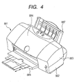
- a liquid discharge head includes at least a liquid chamber having a vibration portion provided with the piezoelectric element or the multilayered piezoelectric element, and an ejection port communicating to the liquid chamber.
- a liquid to be discharged by the liquid discharge head of the present invention as long as the liquid is a fluent material, and the liquid discharge head can discharge an aqueous liquid or a non-aqueous liquid, such as water, ink, or fuel.
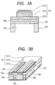
- FIGS. 3A and 3B are schematic views each illustrating a configuration of the liquid discharge head according to an embodiment of the present invention.
- the liquid discharge head of the present invention is a liquid discharge head having a piezoelectric element 101 of the present invention.
- the piezoelectric element 101 includes at least a first electrode 1011, a piezoelectric material 1012, and a second electrode 1013.
- the piezoelectric material 1012 is patterned as necessary.
- FIG. 3B is a schematic view of the liquid discharge head.
- the liquid discharge head includes ejection ports 105, individual liquid chambers 102, communicating holes 106 for connecting the individual liquid chambers 102 and the ejection ports 105, liquid chamber partition walls 104, a common liquid chamber 107, a diaphragm 103, and the piezoelectric elements 101.
- Each of the piezoelectric elements 101 which has a rectangular shape in FIG. 3B , may have a shape except the rectangular shape such as an elliptical shape, a circular shape, or a parallelogram shape.
- the piezoelectric material 1012 has a shape in conformity with the shape of the individual liquid chamber 102.
- FIG. 3A is a sectional view of the piezoelectric element in the width direction of the liquid discharge head illustrated in FIG. 3B .
- the sectional shape of the piezoelectric element 101 which is illustrated in a rectangular shape, may be a trapezoidal shape or a reverse trapezoidal shape.
- the first electrode 1011 is used as the lower electrode, and the second electrode 1013 is used as the upper electrode.
- the arrangement of the first electrode 1011 and the second electrode 1013 is not limited to the foregoing.
- the first electrode 1011 may be used as the lower electrode, or may be used as the upper electrode.
- the second electrode 1013 may be used as the upper electrode, or may be used as the lower electrode.
- a buffer layer 108 may be present between the diaphragm 103 and the lower electrode. Note that, those differences in name depend on a manufacturing method for the device and an effect of the present invention can be obtained in any case.
- the diaphragm 103 vertically fluctuates owing to the expansion and contraction of the piezoelectric material 1012 to apply a pressure to liquid in the individual liquid chamber 102. As a result, the liquid is discharged from the ejection port 105.
- the liquid discharge head of the present invention can be used in a printer application or the manufacture of an electronic apparatus.
- the diaphragm 103 has a thickness of 1.0 ⁇ m or more to 15 ⁇ m or less, preferably 1.5 ⁇ m or more to 8 ⁇ m or less.
- a material for the diaphragm 103, which is not limited, is preferably Si. Si for the diaphragm 103 may be doped with boron or phosphorus.
- the buffer layer and the electrode layer on the diaphragm 103 may serve as part of the diaphragm 103.
- the buffer layer 108 has a thickness of 5 nm or more to 300 nm or less, preferably 10 nm or more to 200 nm or less.
- the size of the ejection port 105 is 5 ⁇ m or more to 40 ⁇ m or less in terms of an equivalent circular diameter.
- the shape of the ejection port 105 may be a circular shape, or may be a star shape, a square shape, or a triangular shape.
- the liquid discharge device of the present invention includes a conveyance portion for a recording medium and the liquid discharge head.
- FIG. 5 illustrates a liquid discharge device (ink jet recording device) 881 illustrated in FIG. 4 in a state in which sheathings 882 to 885 and 887 thereof are removed.
- the ink jet recording device 881 includes an automatic sheet feeder portion 897 for automatically feeding recording sheets as recording media into a device main body 896.
- the ink jet recording device 881 includes a conveyance portion 899 for guiding the recording sheet fed from the automatic sheet feeder portion 897 to a predetermined recording position and from the recording position to an exhaust port 898, a recording portion 891 for performing recording on the recording sheet conveyed to the recording position, and a recovery portion 890 for performing a recovery process on the recording portion 891.
- the recording portion 891 includes a carriage 892 that contains the liquid discharge head of the present invention and is reciprocated on a rail.
- the carriage 892 is moved on the rail based on an electric signal sent from a computer, and a drive voltage is applied to electrodes sandwiching a piezoelectric material so that the piezoelectric material is displaced.
- This displacement of the piezoelectric material pressurizes each individual liquid chamber 102 via the diaphragm 103 illustrated in FIG. 3B , and hence ink is discharged from the ejection port 105 so as to perform printing.
- the liquid discharge device of the present invention can discharge liquid uniformly at high speed, and hence the device can be downsized.
- the printer is exemplified.
- the liquid discharge device of the present invention can be used as a printing device such as an ink jet recording device including a facsimile, a multifunction peripheral, a copying machine, and the like, or as an industrial liquid discharge device or a drawing apparatus for an object.
- An ultrasonic motor includes at least a vibration body provided with the piezoelectric element or the multilayered piezoelectric element, and a moving body to be brought into contact with the vibration body.
- FIGS. 6A and 6B are schematic views each illustrating a configuration of the ultrasonic motor according to an embodiment of the present invention.
- FIG. 6A illustrates the ultrasonic motor in which the piezoelectric element of the present invention is formed of a single plate.
- the ultrasonic motor includes an oscillator 201, a rotor 202, which is brought into contact with the sliding surface of the oscillator 201 with a pressure applied from a pressurizing spring (not shown), and an output shaft 203 provided so as to be integral with the rotor 202.
- the oscillator 201 is formed of a metal elastic ring 2011, a piezoelectric element 2012 of the present invention, and an organic adhesive 2013 for bonding the piezoelectric element 2012 to the elastic ring 2011 (such as an epoxy- or cyanoacrylate-based adhesive).
- the piezoelectric element 2012 of the present invention is formed of a piezoelectric material sandwiched between a first electrode (not shown) and a second electrode (not shown).
- the application of two alternating voltages different from each other in phase by n/2 to the piezoelectric element of the present invention results in the generation of a flexural traveling wave in the oscillator 201, and hence each point on the sliding surface of the oscillator 201 undergoes an elliptical motion.
- the rotor 202 When the rotor 202 is brought into press contact with the sliding surface of the oscillator 201, the rotor 202 receives a frictional force from the oscillator 201 to rotate in the direction opposite to the flexural traveling wave.
- a body to be driven (not shown) is joined to the output shaft 203, and is driven by the rotary force of the rotor 202.
- the application of a voltage to the piezoelectric material results in the expansion and contraction of the piezoelectric material due to a transverse piezoelectric effect.
- an elastic body such as a metal is joined to the piezoelectric element, the elastic body is bent by the expansion and contraction of the piezoelectric material.
- the ultrasonic motor of the kind described here utilizes this principle.
- FIG. 6B An ultrasonic motor including a piezoelectric element having a multilayered structure is illustrated in FIG. 6B .
- An oscillator 204 is formed of a multilayered piezoelectric element 2042 sandwiched between tubular metal elastic bodies 2041.
- the multilayered piezoelectric element 2042 is an element formed of multiple stacked piezoelectric materials (not shown), and includes a first electrode and a second electrode on its outer surfaces of the stack, and internal electrodes on its inner surface of the stack.
- the metal elastic bodies 2041 are fastened with bolts so that the piezoelectric element 2042 may be sandwiched between and fixed by the bodies.
- the oscillator 204 is formed.
- the application of alternating voltages different from each other in phase to the piezoelectric element 2042 causes the oscillator 204 to excite two vibrations orthogonal to each other.
- the two vibrations are combined to form a circular vibration for driving the tip portion of the oscillator 204.
- a constricted annular groove is formed in the upper portion of the oscillator 204 to enlarge the displacement of the vibration for driving.
- a rotor 205 is brought into contact with the oscillator 204 under a pressure from a spring 206 for pressurization to obtain a frictional force for driving.
- the rotor 205 is rotatably supported by a bearing.
- the optical device of the present invention includes a drive portion including the ultrasonic motor.
- FIGS. 7A and 7B are sectional diagrams of main parts of an interchangeable lens barrel for a single-lens reflex camera as an example of an imaging device according to a preferred embodiment of the present invention.
- FIG. 8 is an exploded perspective diagram of the interchangeable lens barrel for the single-lens reflex camera as the example of the imaging device according to the preferred embodiment of the present invention.
- a fixed barrel 712, a linear guide barrel 713, and a front unit barrel 714 are fixed to an attaching/detaching mount 711 for a camera. These are fixed members of the interchangeable lens barrel.
- a linear guide groove 713a in an optical axis direction for a focus lens 702 is formed on the linear guide barrel 713.
- Cam rollers 717a and 717b protruding outward in a radial direction are fixed to a rear unit barrel 716 supporting the focus lens 702 via axial screws 718, and the cam roller 717a is fitted in the linear guide groove 713a.
- a cam ring 715 is fitted on the inner periphery of the linear guide barrel 713 in a rotatable manner. Relative movement between the linear guide barrel 713 and the cam ring 715 in the optical axis direction is restricted because a roller 719 fixed to the cam ring 715 is fitted in an annular groove 713b of the linear guide barrel 713.
- a cam groove 715a for the focus lens 702 is formed on the cam ring 715, and the above-mentioned cam roller 717b is simultaneously fitted in the cam groove 715a.
- a rotation transmission ring 720 supported by a ball race 727 in a rotatable manner at a constant position with respect to the fixed barrel 712.
- the rotation transmission ring 720 has shafts 720f extending radially from the rotation transmission ring 720, and rollers 722 are supported by the shafts 720f in a rotatable manner.
- a large diameter part 722a of the roller 722 is brought into contact with a mount side end surface 724b of a manual focus ring 724.
- a small diameter part 722b of the roller 722 is brought into contact with a joining member 729.
- Six rollers 722 are disposed on the outer periphery of the rotation transmission ring 720 at uniform intervals, and each roller is provided in the relationship as described above.
- a low friction sheet (washer member) 733 is disposed on an inner diameter part of the manual focus ring 724, and this low friction sheet is sandwiched between a mount side end surface 712a of the fixed barrel 712 and a front side end surface 724a of the manual focus ring 724.
- an outer diameter surface of the low friction sheet 733 is formed in a ring shape so as to be circumferentially fitted on an inner diameter part 724c of the manual focus ring 724.
- the inner diameter part 724c of the manual focus ring 724 is circumferentially fitted on an outer diameter part 712b of the fixed barrel 712.
- the low friction sheet 733 has a role of reducing friction in a rotation ring mechanism in which the manual focus ring 724 rotates relatively to the fixed barrel 712 about the optical axis.
- the large diameter part 722a of the roller 722 is brought into contact with the mount side end surface 724b of the manual focus ring in a state in which a pressure is applied by a pressing force of a waved washer 726 pressing an ultrasonic motor 725 to the front of the lens.
- the small diameter part 722b of the roller 722 is brought into contact with the joining member 729 in a state in which an appropriate pressure is applied by a pressing force of the waved washer 726 pressing the ultrasonic motor 725 to the front of the lens.
- Movement of the waved washer 726 in the mount direction is restricted by a washer 732 connected to the fixed barrel 712 by bayonet joint.
- a spring force (biasing force) generated by the waved washer 726 is transmitted to the ultrasonic motor 725, and further to the roller 722, to be a force for the manual focus ring 724 to press the mount side end surface 712a of the fixed barrel 712.
- the manual focus ring 724 is integrated in a state in which the manual focus ring 724 is pressed to the mount side end surface 712a of the fixed barrel 712 via the low friction sheet 733.
- the rollers 722 rotate about the shafts 720f by friction force because the mount side end surface 724b of the manual focus ring 724 is brought into contact by pressure to the large diameter parts 722a of the rollers 722.
- the rotation transmission ring 720 rotates about the optical axis.
- the ultrasonic motor 725 does not rotate because of a friction retaining force between a rotor 725c and a stator 725b (manual focus operation).
- Two focus keys 728 are mounted to the rotation transmission ring 720 at opposing positions, and the focus key 728 is fitted to a notch portion 715b disposed on the tip of the cam ring 715. Therefore, when the automatic focus operation or the manual focus operation is performed so that the rotation transmission ring 720 is rotated about the optical axis, the rotation force is transmitted to the cam ring 715 via the focus key 728.
- the cam ring is rotated about the optical axis, the rear unit barrel 716 whose rotation is restricted by the cam roller 717a and the linear guide groove 713a is moved forward and backward along the cam groove 715a of the cam ring 715 by the cam roller 717b. Thus, the focus lens 702 is driven, and the focus operation is performed.
- the interchangeable lens barrel for the single-lens reflex camera is described above as the optical device of the present invention, but the present invention can be applied to any optical device including the drive portion including the ultrasonic motor, regardless of a type of the camera, including a compact camera, an electronic still camera, a personal digital assistant with camera, and the like.
- a vibration device used for conveying or removing particles, powder, or liquid droplets is used widely for an electronic apparatus or the like.
- a dust removing device includes a vibration body including a diaphragm including the piezoelectric element or the multilayered piezoelectric element.
- FIGS. 9A and 9B are schematic views each illustrating a dust removing device according to an embodiment of the present invention.
- a dust removing device 310 is formed of a plate-like piezoelectric element 330 and a diaphragm 320.
- the piezoelectric element 330 may be the multilayered piezoelectric element of the present invention.
- the material of the diaphragm 320 is not limited. In the case where the dust removing device 310 is used for an optical device, a transparent material or a reflective material can be used as the material of the diaphragm 320.
- FIGS. 10A to 10C are schematic views illustrating a configuration of the piezoelectric element 330 illustrated in FIGS. 9A and 9B .
- FIGS. 10A and 10C illustrate a front surface configuration and a rear surface configuration of the piezoelectric element 330, respectively.
- FIG. 10B illustrates a side surface configuration.
- the piezoelectric element 330 includes a piezoelectric material 331, a first electrode 332, and a second electrode 333.
- the first electrode 332 and the second electrode 333 are disposed so as to be opposed to each other on the plate planes of the piezoelectric material 331.
- the piezoelectric element 330 may be the multilayered piezoelectric element of the present invention.
- the piezoelectric material 331 has an alternate structure of a piezoelectric material layer and an internal electrode and can provide driving waveforms different from each other in phase depending on the piezoelectric material layers by short-circuiting the internal electrode with the first electrode 332 or the second electrode 333 alternately.
- the front plane of the piezoelectric element 330 illustrated in FIG. 10C on which the first electrode 332 is disposed, is referred to as a first electrode plane 336.
- the front plane of the piezoelectric element 330 illustrated in FIG. 10A on which the second electrode 333 is disposed, is referred to as a second electrode plane 337.
- the electrode plane in the present invention means a plane of the piezoelectric element on which the electrode is disposed.
- the first electrode 332 may extend around to the second electrode plane 337.
- the plate surface of the diaphragm 320 is fixed to the first electrode plane 336 of the piezoelectric element 330.
- the dust removing device 310 of the present invention is a device that removes foreign matters such as dust sticking to the surface of the diaphragm 320 by the out-of-plane oscillation of the diaphragm 320.
- the out-of-plane oscillation means elastic oscillation in which the diaphragm is displaced in the optical axis direction, namely in the thickness direction of the diaphragm.
- FIGS. 11A and 11B are schematic views illustrating a vibration principle of the dust removing device 310 of the present invention.
- FIG. 11A illustrates a state in which alternating electric fields having the same phase are applied to a pair of left and right piezoelectric elements 330 so that the out-of-plane oscillation is generated in the diaphragm 320.
- the polarization direction of the piezoelectric material forming the pair of left and right piezoelectric elements 330 is the same as the thickness direction of the piezoelectric elements 330, and the dust removing device 310 is driven by the seventh oscillation mode.
- FIG. 11B illustrates a state in which alternating voltages having reverse phases by 180 degrees are applied to the pair of left and right piezoelectric elements 330 so that the out-of-plane oscillation is generated in the diaphragm 320.
- the dust removing device 310 is driven by the sixth oscillation mode.
- the dust removing device 310 of the present invention is a device that can effectively remove dust sticking to the surface of the diaphragm by using at least two oscillation modes selectively.
- an imaging device of the present invention is described.
- the imaging device of the present invention is an imaging device including at least the dust removing device and an image pickup element unit.
- the diaphragm of the dust removing device is disposed on a side of a light receiving plane of the image pickup element unit.
- FIGS. 12 and 13 are diagrams each illustrating a digital single-lens reflex camera as an example of an imaging device according to a preferred embodiment of the present invention.
- FIG. 12 is a front side perspective diagram of a camera main body 601 viewed from an object side, in which an imaging lens unit is removed.
- FIG. 13 is an exploded perspective diagram illustrating an internal schematic configuration of the camera for describing a peripheral structure of the dust removing device and an image pickup unit 400 of the present invention.
- a mirror box 605 for guiding an imaging light beam that has passed through the imaging lens is disposed in the camera main body 601, and a main mirror (quick return mirror) 606 is disposed in the mirror box 605.
- the main mirror 606 can take one of states including a state of being supported at an angle of 45 degrees with respect to an imaging optical axis in order to guide the imaging light beam in the direction to a penta-dach mirror (not shown) and a state of being retreated from the imaging light beam in order to guide the imaging light beam in the direction to an image pickup element (not shown).
- the mirror box 605 and a shutter unit 200 are disposed in order from the object side.
- the image pickup unit 400 is disposed on a photographer side of the main body chassis 300.
- the image pickup unit 400 is adjusted and disposed so that the imaging surface of the image pickup element is parallel to a mounting surface of a mount portion 602 to be a reference for mounting the imaging lens unit with a predetermined distance.
- the digital single-lens reflex camera is described above as the imaging device of the present invention, but the device may be a camera with interchangeable imaging lens unit such as a mirrorless digital single-lens camera without the mirror box 605, for example.
- the present invention can be applied to various types of imaging devices or electronic and electric devices including the imaging device, such as a video camera with interchangeable imaging lens unit, a copying machine, a facsimile, and a scanner, in particular, a device that is required to remove dust sticking to a surface of an optical component.
- the electronic apparatus of the present invention includes a piezoelectric acoustic component including the piezoelectric element or the multilayered piezoelectric element.
- Examples of the piezoelectric acoustic component include a speaker, a buzzer, a microphone, and a surface acoustic wave (SAW) element.
- SAW surface acoustic wave
- FIG. 14 is a general perspective diagram of a main body 931 of a digital camera as an example of an electronic apparatus according to a preferred embodiment of the present invention, as viewed from the front.
- an optical device 901 On a front surface of the main body 931, there are disposed an optical device 901, a microphone 914, a stroboscopic light emission portion 909, and a fill light portion 916. Because the microphone 914 is installed in the main body, the microphone 914 is illustrated by a broken line. In the front of the microphone 914, there is a hole shape provided for collecting external sound.
- a power button 933, a speaker 912, a zoom lever 932, and a release button 908 for performing a focus operation are disposed on the top surface of the main body 931.
- the speaker 912 is installed in the main body 931 and is illustrated by a broken line. In the front of the speaker 912, there is a hole shape provided for transmitting sound to the outside.
- the piezoelectric acoustic component of the present invention is used for at least one of the microphone 914, the speaker 912, and the surface acoustic wave element.
- the digital camera is described above as the electronic apparatus of the present invention, but the present invention can also be applied to various types of the electronic apparatus including the piezoelectric acoustic component, such as a sound reproduction device, a sound recording device, a mobile phone, or an information terminal.
- the piezoelectric acoustic component such as a sound reproduction device, a sound recording device, a mobile phone, or an information terminal.
- the piezoelectric element and the multilayered piezoelectric element of the present invention can be preferably used in a liquid discharge head, a liquid discharge device, an ultrasonic motor, an optical device, a vibration device, a dust removing device, an imaging device, and an electronic apparatus.
- the piezoelectric element and the multilayered piezoelectric element of the present invention it is possible to provide the liquid discharge head having the same or higher nozzle density and discharge speed than the case where the piezoelectric element containing lead is used.
- liquid discharge head of the present invention Through the use of the liquid discharge head of the present invention, it is possible to provide the liquid discharge device having the same or higher discharge speed and discharge accuracy than the case where the piezoelectric element containing lead is used.
- the piezoelectric element and the multilayered piezoelectric element of the present invention it is possible to provide the ultrasonic motor having the same or higher driving force and durability than the case where the piezoelectric element containing lead is used.
- the ultrasonic motor of the present invention it is possible to provide the optical device having the same or higher durability and operation accuracy than the case where the piezoelectric element containing lead is used.
- the piezoelectric element and the multilayered piezoelectric element of the present invention it is possible to provide the vibration device having the same or higher vibration performance and durability than the case where the piezoelectric element containing lead is used.
- the vibration device of the present invention Through the use of the vibration device of the present invention, it is possible to provide the dust removing device having the same or higher dust-removing efficiency and durability than the case where the piezoelectric element containing lead is used.
- the dust removing device of the present invention it is possible to provide the imaging device having the same or higher dust-removing function than the case where the piezoelectric element containing lead is used.
- the piezoelectric acoustic component including the piezoelectric element or the multilayered piezoelectric element of the present invention it is possible to provide the electronic apparatus having the same or higher sound producing performance than the case where the piezoelectric element containing lead is used.
- the piezoelectric material of the present invention can be used in such a device as an ultrasonic oscillator, a piezoelectric actuator, a piezoelectric sensor, and a ferroelectric memory, as well as the liquid discharge head and the motor.
- the piezoelectric material of the present invention is described more specifically by way of examples.
- the present invention is not limited by the following examples.
- a piezoelectric material for evaluation was polished so that the thickness thereof became about 0.5 mm.
- the density of the piezoelectric material was evaluated by Archimedes method. When the density was equal to or more than 95% of the theoretical density, it was determined that the piezoelectric material was sufficiently crystallized.
- the crystal phase and lattice constant of the piezoelectric material were evaluated by X-ray diffraction measurement.
- a metal oxide material for comparison formed of NN-BT and free of Bi, K, and Cu was produced.
- Sodium niobate (NaNbO 3 ) powder and barium titanate (BaTiO 3 ) powder were used as raw materials.
- Sodium niobate (NaNbO 3 ) having a purity of 99% or more was used as the sodium niobate powder, and barium titanate (BaTiO 3 ) having a purity of 99% or more was used as the barium titanate powder.
- the mixed powder was calcined at 1,000 to 1,100°C in the air for 2 to 5 hours.
- the calcined powder was crushed, and a binder was added thereto, followed by granulation.
- the granulated powder was filled in a mold and was compressed to manufacture a compact having a diameter of 17 mm and a thickness of about 1 mm.
- a sintered body was obtained.
- the surface of the obtained sintered body was observed with an optical microscope to evaluate a grain size. As a result, it was found that the grain size was 0.5 ⁇ m to 60 ⁇ m.
- the density of the sintered body was 95% or more of the theoretical density.
- the composition of the sintered body was evaluated by inductively coupled plasma optical emission spectrometry (ICP). As a result, it was found that sodium was insufficient by about 1% to 5% from the intended composition.
- the compositions of barium, niobium, and titanium were the same as the intended compositions.
- Sodium niobate (NaNbO 3 ) powder, barium titanate (BaTiO 3 ) powder, and bismuth potassium titanate ((Bi 0.5 K 0.5 )TiO 3 ) powder were used as raw materials.
- Sodium niobate (NaNbO 3 ) having a purify of 99% or more was used as the sodium niobate powder
- barium titanate (BaTiO 3 ) having a purity of 99% or more was used as the barium titanate powder
- bismuth potassium titanate ((Bi 0.5 K 0.5 )TiO 3 ) having a purity of 99% or more was used as the bismuth potassium titanate powder
- copper oxide (CuO(II)) having a purity of 99.9% was used as the Cu.
- the mixed powder was calcined at 900 to 1,000°C in the air for 2 to 5 hours.
- the calcined powder was crushed, and a binder was added thereto, followed by granulation.
- the granulated powder was filled in a mold and was compressed to manufacture a compact having a diameter of 17 mm and a thickness of about 1 mm.
- a sintered body was obtained.
- the surface of the obtained sintered body was observed with an optical microscope to evaluate a grain size. As a result, it was found that the grain size was 0.5 ⁇ m to 50 ⁇ m.
- the sintered piezoelectric material was measured by X-ray diffraction, it was confirmed that the sample was substantially of a perovskite structure single phase.
- the density of the piezoelectric material was 95% or more of the theoretical density.
- the composition of the piezoelectric material was analyzed by the ICP. As a result, it was found that sodium was insufficient by about 3% to 4% from the intended composition.
- the compositions of potassium, bismuth, barium, niobium, titanium, and copper were the same as the intended compositions.
- the sintered piezoelectric material was measured by X-ray diffraction, it was confirmed that the sample was substantially of a perovskite structure single phase.
- the density of the piezoelectric material was 95% or more of the theoretical density.
- the composition of the piezoelectric material was analyzed by the ICP. As a result, it was found that sodium was insufficient by about 4% to 5% from the intended composition.
- the compositions of potassium, bismuth, barium, niobium, titanium, and copper were the same as the intended compositions.
- Samples were each produced as the piezoelectric material of the present invention by a method similar to those of Examples 1 to 8.
- a sintered body was obtained by firing a compact at a maximum temperature of 1,100°C in the air for 1 to 6 hours. The surface of the obtained sintered body was observed with an optical microscope to evaluate a grain size. As a result, it was found that the grain size was 0.5 ⁇ m to 50 ⁇ m.
- the sintered piezoelectric material was measured by X-ray diffraction, it was confirmed that the sample was substantially of a perovskite structure single phase.
- the density of the piezoelectric material was 95% or more of the theoretical density.
- the composition of the piezoelectric material was analyzed by the ICP. As a result, it was found that sodium was insufficient by about 1% to 2% from the intended composition.
- the compositions of potassium, bismuth, barium, niobium, titanium, and copper were the same as the intended compositions.
- a sintered body was obtained by firing a compact at a maximum temperature of 1,100°C in the air for 1 to 6 hours. The surface of the obtained sintered body was observed with an optical microscope to evaluate a grain size. As a result, it was found that the grain size was 0.5 ⁇ m to 50 ⁇ m.
- a sintered body was obtained by firing a compact at a maximum temperature of 1,150°C in the air for 1 to 6 hours. The density of the obtained sintered body was less than 93% of the theoretical density and its insulation resistance was also low owing to the insufficient sintering, with the result that the sintered body was not able to be subjected to polarization treatment.
- the sintered piezoelectric material was measured by X-ray diffraction, it was confirmed that the sample was substantially of a perovskite structure single phase.
- the density of the piezoelectric material was 93% or more of the theoretical density.
- the composition of the piezoelectric material was analyzed by the ICP. As a result, it was found that sodium was insufficient by about 1% to 5% from the intended composition.
- the compositions of potassium, bismuth, barium, niobium, titanium, and copper were the same as the intended compositions.
- each of the piezoelectric materials of Examples 1 to 12 was polished and subjected to heat treatment at 400 to 1,000°C in the air for 1 hour so as to remove an organic component on the surface.
- Gold electrodes were formed on front and rear surfaces of the piezoelectric material by DC sputtering to obtain the piezoelectric element of the present invention.
- the resultant piezoelectric element was processed into a strip shape having a size of 10 mmx2.5 mm ⁇ 0.5 mm and evaluated for various characteristics.
- the metal oxide materials of Comparative Examples 1 to 6 were processed in the same way as in Examples 1 to 12 to obtain elements for comparison. These elements for comparison were evaluated for various characteristics.
- a resistivity For measuring a resistivity, an unpolarized element was used. A direct current bias of 10 V was applied between the two electrodes of the element, and a resistivity was obtained from a leaked current value after 20 seconds.
- this resistivity is 1 G ⁇ cm or more, preferably 100 G ⁇ cm or more, the sample has insulation property sufficient for practical use of a piezoelectric material and a piezoelectric element.
- the sample Prior to the evaluation of piezoelectricity, the sample was subjected to polarization treatment. Specifically, the sample was heated to 100°C to 150°C in an oil bath, and a voltage of 20 kV/cm was applied to the sample for 30 minutes. Then, the sample was cooled to room temperature while the voltage was applied thereto.
- the piezoelectric constant (d 31 ) and mechanical quality factor (Qm) of a piezoelectric material were evaluated by a resonance-antiresonance method through use of the strip-shaped piezoelectric element.
- the temperature at which a relative dielectric constant became a local maximum was measured, and this temperature was defined as a Curie temperature.
- Table 1 shows each composition ratio, resistivity, Curie temperature, mechanical quality factor (Qm), Young's modulus (Y 11 ), and piezoelectric constant (d31) at a time of charging and after firing of the piezoelectric elements obtained from the piezoelectric materials of Examples 1 to 12 and the elements obtained from the metal oxide materials of Comparative Examples 1 to 6.
- x' represents a composition ratio at a time of charging
- x represents a composition ratio after firing.
- the y, v and w representing the composition ratios of Nb, K and Bi, and the addition amount of Cu substantially remained unchanged between the time of charging and the time after firing.
- compositions of Comparative Examples 1 to 3 was free of Cu, and hence sufficient insulation resistance was not obtained even when the metal oxide materials were fired at a temperature lower than 1,200°C, with the result that the elements were not able to be subjected to polarization treatment.
- Powders of raw materials were subjected to wet mixing and dehydration drying in the same way as in Example 2, followed by calcination at 900°C to 1,000°C to obtain a calcined product.
- An organic binder was added to the resultant raw material, followed by mixing, and thereafter, a sheet was formed by a doctor blade method to obtain a green sheet having a thickness of 50 ⁇ m.
- a conductive paste for an internal electrode was printed onto the green sheet.
- As the conductive paste an alloy containing 70% of Ag and 30% of Pd was used.
- Nine green sheets coated with the conductive paste thus produced were stacked, and the multilayered body was fired at 1,140°C to obtain a sintered body.
- the sintered body thus obtained was cut to a size of 10 mmx2.5 mm, and side surfaces thereof were then polished.
- a pair of external electrodes (first electrode and second electrode) for short-circuiting internal electrodes alternately was formed by Au sputtering to produce a multilayered piezoelectric element as illustrated in FIG. 2B .
- the internal electrodes of the obtained multilayered piezoelectric element were observed. As a result, it was found that Ag-Pd as an electrode material and a piezoelectric material layer were formed alternately.
- the sample Prior to the evaluation of piezoelectricity, the sample was subjected to polarization treatment. Specifically, the sample was heated to 100°C to 150°C on a hot plate. A voltage of 20 kV/cm was applied between the first electrode and the second electrode for 30 minutes, and the sample was cooled to room temperature while the voltage was applied thereto.
- the piezoelectricity was evaluated. As a result, it was found that the sample had sufficient insulation property and satisfactory piezoelectric property equivalent to that of the piezoelectric material of Example 4 was obtained.
- Powders of raw materials were subjected to wet mixing and dehydration drying in the same way as in Comparative Example 1, followed by calcination at 1,000°C to 1, 100°C to obtain a calcined product.
- An organic binder was added to the resultant raw material, followed by mixing, and thereafter, a sheet was formed by a doctor blade method to obtain a green sheet having a thickness of 50 pm.
- a conductive paste for an internal electrode was printed onto the green sheet.
- As the conductive paste an alloy containing 70% of Ag and 30% of Pd was used.
- Nine green sheets coated with the conductive paste thus produced were stacked, and the multilayered body was fired at 1,280°C to obtain a sintered body.
- the sintered body thus obtained was processed in the same way as in Example 13 to produce a multilayered piezoelectric element as illustrated in FIG. 2B .
- the internal electrodes of the obtained multilayered piezoelectric element were observed. As a result, it was found that Ag-Pd as an electrode material was melted due to the high sintering temperature, and Ag and Pd were dispersed in the piezoelectric material layer. Further, a resistivity between the pair of external electrodes of the element was low, i.e., 10 6 ⁇ cm or less, and hence a piezoelectric constant was not able to be measured.
- a green sheet having a thickness of 50 ⁇ m was obtained in the same way as in Comparative Example 8.
- a conductive paste for an internal electrode was printed onto the green sheet.
- As the conductive paste an alloy containing 95% of Ag and 5% of Pd was used.
- Nine green sheets coated with the conductive paste thus produced were stacked, and the multilayered body was fired at 1,300°C to obtain a sintered body.
- the sintered body thus obtained was processed in the same way as in Example 13 to produce a multilayered piezoelectric element as illustrated in FIG. 2B .
- the internal electrodes of the obtained multilayered piezoelectric element were observed. As a result, it was found that the internal electrodes were melted and scatted like islands. Thus, the internal electrodes were not brought into conduction, and hence the multilayered piezoelectric element was not able to be subjected to polarization treatment. Therefore, a piezoelectric constant was not able to be measured.
- Sodium niobate powder, barium titanate powder, and barium zirconate powder were weighed so that Na, Nb, Ba, and Zr had the compositions described in Example 2 in Table 1.
- the weighed raw material powders were mixed overnight with a ball mill.
- 3 parts by weight of a PVB binder were added and mixed.
- a sheet was formed by a doctor blade method through use of the mixed powder to obtain a green sheet having a thickness of 50 ⁇ m.
- a conductive paste for an internal electrode was printed on the green sheet.
- As the conductive paste an Ni paste was used.
- Nine green sheets coated with the conductive paste were stacked, and the multilayered body was subjected to thermocompression bonding.
- the multilayered body subjected to thermocompression bonding was fired in a tubular furnace.
- the firing was performed in the atmosphere up to 300°C to remove the binder.
- the oxygen concentration was changed to 30 Pa at 1,000°C or less, and the multilayered body was cooled to room temperature.
- the thus obtained sintered body was cut to a size of 10 mmx2.5 mm, and side surfaces thereof were polished.
- a pair of external electrodes (first electrode and second electrode) for short-circuiting internal electrodes alternately was formed by Au sputtering to produce a multilayered piezoelectric element as illustrated in FIG. 3B .
- the internal electrodes of the obtained multilayered piezoelectric element were observed. As a result, it was found that Ni as an electrode material and a piezoelectric material layer were formed alternately.
- the obtained multilayered piezoelectric element was subjected to polarization treatment by applying an electric field of 2 kV/mm to the multilayered piezoelectric element in an oil bath held at 150°C for 30 minutes.
- the piezoelectric property of the obtained multilayered piezoelectric element was evaluated. As a result, sufficient insulation property was obtained, and satisfactory piezoelectric property equivalent to that of the piezoelectric element of Example 2 was obtained.
- Example 2 Through the use of the piezoelectric element of Example 2, the liquid discharge head illustrated in FIGS. 3A and 3B was manufactured. It was confirmed that ink was discharged in accordance with an input electric signal.
- Example 15 Through the use of the liquid discharge head of Example 15, the liquid discharge device illustrated in FIG. 4 was manufactured. It was confirmed that ink was discharged on a recording medium in accordance with an input electric signal.
- Example 2 Through the use of the piezoelectric element of Example 2, the ultrasonic motor illustrated in FIG. 6A was manufactured. It was confirmed that the motor rotated in accordance with an applied alternating voltage.
- Example 17 Through the use of the ultrasonic motor of Example 17, the optical device illustrated in FIGS. 7A and 7B was manufactured. It was confirmed that the automatic focus operation was performed in accordance with an applied alternating voltage.
- the dust removing device illustrated in FIGS. 9A and 9B was manufactured. Plastic beads were scattered, and an alternating voltage was applied. Then, satisfactory dust removing efficiency was confirmed.
- Example 19 Through the use of the dust removing device of Example 19, the imaging device illustrated in FIG. 12 was manufactured. During operation, the dust on the surface of the image pickup unit was satisfactorily removed, and an image without a dust defect was obtained.
- Example 13 Through the use of the multilayered piezoelectric element of Example 13, the liquid discharge head illustrated in FIGS. 3A and 3B was manufactured. It was confirmed that ink was discharged in accordance with an input electric signal.
- Example 21 Through the use of the liquid discharge head of Example 21, the liquid discharge device illustrated in FIG. 4 was manufactured. It was confirmed that ink was discharged on a recording medium in accordance with an input electric signal.
- Example 13 Through the use of the multilayered piezoelectric element of Example 13, the ultrasonic motor illustrated in FIG. 6B was manufactured. It was confirmed that the motor rotated in accordance with an applied alternating voltage.
- Example 23 Through the use of the ultrasonic motor of Example 23, the optical device illustrated in FIGS. 7A and 7B was manufactured. It was confirmed that the automatic focus operation was performed in accordance with an applied alternating voltage.
- the dust removing device illustrated in FIGS. 9A and 9B was manufactured. Plastic beads were scattered, and an alternating voltage was applied. Then, satisfactory dust removing efficiency was confirmed.
- Example 25 Through the use of the dust removing device of Example 25, the imaging device illustrated in FIG. 12 was manufactured. During operation, the dust on the surface of the image pickup unit was satisfactorily removed, and an image without a dust defect was obtained.
- Example 13 Through the use of the multilayered piezoelectric element of Example 13, the electronic apparatus illustrated in FIG. 14 was manufactured. It was confirmed that the speaker operated in accordance with an applied alternating voltage.
- the piezoelectric material of the present invention expresses satisfactory piezoelectricity even at high ambient temperature.
- the piezoelectric material of the present invention has a small load on the environment because it is free of lead. Accordingly, the lead-free piezoelectric material of the present invention can be used without any problem for devices using a great amount of piezoelectric material such as a liquid discharge head, a liquid discharge device, an ultrasonic motor, an optical device, a vibration device, a dust removing device, an imaging device, and an electronic apparatus.
Landscapes
- Engineering & Computer Science (AREA)
- Chemical & Material Sciences (AREA)
- Ceramic Engineering (AREA)
- Manufacturing & Machinery (AREA)
- Materials Engineering (AREA)
- Structural Engineering (AREA)
- Organic Chemistry (AREA)
- Inorganic Chemistry (AREA)
- Physics & Mathematics (AREA)
- General Physics & Mathematics (AREA)
- Optics & Photonics (AREA)
- Mechanical Engineering (AREA)
- Composite Materials (AREA)
- Particle Formation And Scattering Control In Inkjet Printers (AREA)
- General Electrical Machinery Utilizing Piezoelectricity, Electrostriction Or Magnetostriction (AREA)
- Compositions Of Oxide Ceramics (AREA)
- Piezo-Electric Transducers For Audible Bands (AREA)
- Lens Barrels (AREA)
- Camera Bodies And Camera Details Or Accessories (AREA)
Applications Claiming Priority (2)
| Application Number | Priority Date | Filing Date | Title |
|---|---|---|---|
| JP2012186643 | 2012-08-27 | ||
| PCT/JP2013/072927 WO2014034692A1 (en) | 2012-08-27 | 2013-08-21 | Piezoelectric material and piezoelectric element using the same, and electronic apparatus using the piezoelectronic element |
Publications (2)
| Publication Number | Publication Date |
|---|---|
| EP2873103A1 EP2873103A1 (en) | 2015-05-20 |
| EP2873103B1 true EP2873103B1 (en) | 2020-10-28 |
Family
ID=49162184
Family Applications (1)
| Application Number | Title | Priority Date | Filing Date |
|---|---|---|---|
| EP13760118.3A Active EP2873103B1 (en) | 2012-08-27 | 2013-08-21 | Piezoelectric material and piezoelectric element using the same, and electronic apparatus using the piezoelectronic element |
Country Status (7)
| Country | Link |
|---|---|
| US (1) | US9660174B2 (zh) |
| EP (1) | EP2873103B1 (zh) |
| JP (1) | JP6180234B2 (zh) |
| KR (1) | KR101728255B1 (zh) |
| CN (1) | CN104584249B (zh) |
| TW (1) | TWI500191B (zh) |
| WO (1) | WO2014034692A1 (zh) |
Families Citing this family (11)
| Publication number | Priority date | Publication date | Assignee | Title |
|---|---|---|---|---|
| JP6327087B2 (ja) * | 2014-09-25 | 2018-05-23 | Tdk株式会社 | 圧電組成物、圧電素子およびスパッタリングターゲット |
| JP6575743B2 (ja) * | 2015-01-30 | 2019-09-18 | セイコーエプソン株式会社 | 液体噴射ヘッドの駆動方法及び圧電素子並びに液体噴射ヘッド |
| US10461241B2 (en) * | 2015-03-17 | 2019-10-29 | Canon Kabushiki Kaisha | Method for manufacturing rectangular parallelepiped-shaped single crystal, rectangular parallelepiped-shaped single crystal, method for manufacturing ceramics, ceramics, piezoelectric element, piezoelectric device, and electronic device |
| JP6415474B2 (ja) * | 2015-06-29 | 2018-10-31 | 太陽誘電株式会社 | 誘電体磁器組成物及びそれを有する誘電体素子 |
| CN106739505B (zh) * | 2016-11-09 | 2018-08-14 | 西安交通大学 | 一种复合腔体压电喷墨打印头及其制造方法 |
| JP6958045B2 (ja) * | 2017-07-11 | 2021-11-02 | セイコーエプソン株式会社 | 圧電素子およびその製造方法、ならびに圧電素子応用デバイス |
| JP7057941B2 (ja) | 2017-08-04 | 2022-04-21 | キヤノン株式会社 | 圧電材料、圧電素子、および電子機器 |
| JP7156632B2 (ja) | 2017-08-04 | 2022-10-19 | キヤノン株式会社 | 圧電材料、圧電素子、および電子機器 |
| JP6569922B2 (ja) | 2017-08-04 | 2019-09-04 | キヤノン株式会社 | 圧電材料、圧電素子、および電子機器 |
| US11272080B2 (en) | 2018-02-06 | 2022-03-08 | Canon Kabushiki Kaisha | Vibration device for dust removal and imaging device |
| CN111389322B (zh) * | 2020-03-31 | 2023-07-25 | 华北水利水电大学 | 一种水热-热处理自动化实验平台 |
Family Cites Families (16)
| Publication number | Priority date | Publication date | Assignee | Title |
|---|---|---|---|---|
| JP3635992B2 (ja) | 1999-07-22 | 2005-04-06 | 株式会社村田製作所 | 圧電型電気音響変換器 |
| JP4529902B2 (ja) * | 2003-01-21 | 2010-08-25 | Tdk株式会社 | 薄膜容量素子用組成物、高誘電率絶縁膜、薄膜容量素子、薄膜積層コンデンサおよび薄膜容量素子の製造方法 |
| JP4995412B2 (ja) | 2003-05-29 | 2012-08-08 | 日本特殊陶業株式会社 | 圧電磁器組成物及びこれを用いた圧電素子 |
| CN100337980C (zh) * | 2003-05-29 | 2007-09-19 | 日本特殊陶业株式会社 | 压电陶瓷组合物以及含该组合物的压电元件 |
| JP2009227535A (ja) | 2008-03-25 | 2009-10-08 | Panasonic Corp | 圧電性磁器組成物 |
| JP2011068516A (ja) * | 2009-09-25 | 2011-04-07 | Tdk Corp | 圧電磁器組成物、圧電磁器、圧電素子及び発振子 |
| JP5734688B2 (ja) | 2010-02-10 | 2015-06-17 | キヤノン株式会社 | 配向性酸化物セラミックスの製造方法、配向性酸化物セラミックス、圧電素子、液体吐出ヘッド、超音波モータおよび塵埃除去装置 |
| DE102010009461A1 (de) | 2010-02-26 | 2011-09-01 | Siemens Aktiengesellschaft | Bleifreier, mehrphasiger keramischer Werkstoff mit Texturierung, Verfahren zum Herstellen des Werkstoffs und Verwendung des Werkstoffs |
| KR101556456B1 (ko) * | 2011-02-28 | 2015-10-01 | 캐논 가부시끼가이샤 | 압전 재료, 압전 소자, 액체 토출 헤드, 초음파 모터, 및 먼지 제거 디바이스 |
| JP5865608B2 (ja) * | 2011-05-31 | 2016-02-17 | キヤノン株式会社 | 配向性圧電セラミックス、圧電素子、液体吐出ヘッド、超音波モータおよび塵埃除去装置 |
| JP6080465B2 (ja) * | 2011-10-26 | 2017-02-15 | キヤノン株式会社 | 圧電材料、圧電素子、圧電音響部品、および電子機器 |
| DE102011117709A1 (de) * | 2011-11-04 | 2013-05-08 | Epcos Ag | Keramikmaterial, Verfahren zur Herstellung desselben und elektrokeramisches Bauelement umfassend das Keramikmaterial |
| CN102515762A (zh) * | 2011-12-22 | 2012-06-27 | 四川师范大学 | 铌酸钠钛酸钡铋钾系无铅压电陶瓷组合物 |
| JP6249669B2 (ja) * | 2012-08-27 | 2017-12-20 | キヤノン株式会社 | 圧電材料、圧電素子、および電子機器 |
| TW201434789A (zh) * | 2013-01-29 | 2014-09-16 | Canon Kk | 壓電材料、壓電元件及電子裝備 |
| KR20150115845A (ko) * | 2013-01-29 | 2015-10-14 | 캐논 가부시끼가이샤 | 압전 재료, 압전 소자, 적층 압전 소자, 액체 토출 헤드, 액체 토출 장치, 초음파 모터, 광학 장치, 진동 장치, 먼지 제거 장치, 촬상 장치 및 전자 기기 |
-
2013
- 2013-08-21 US US14/420,135 patent/US9660174B2/en active Active
- 2013-08-21 CN CN201380044036.3A patent/CN104584249B/zh active Active
- 2013-08-21 WO PCT/JP2013/072927 patent/WO2014034692A1/en active Application Filing
- 2013-08-21 KR KR1020157007001A patent/KR101728255B1/ko active IP Right Grant
- 2013-08-21 EP EP13760118.3A patent/EP2873103B1/en active Active
- 2013-08-23 JP JP2013172828A patent/JP6180234B2/ja active Active
- 2013-08-26 TW TW102130431A patent/TWI500191B/zh active
Non-Patent Citations (1)
| Title |
|---|
| None * |
Also Published As
| Publication number | Publication date |
|---|---|
| WO2014034692A1 (en) | 2014-03-06 |
| KR101728255B1 (ko) | 2017-04-18 |
| CN104584249A (zh) | 2015-04-29 |
| CN104584249B (zh) | 2017-10-27 |
| JP6180234B2 (ja) | 2017-08-16 |
| JP2014062034A (ja) | 2014-04-10 |
| US20150194594A1 (en) | 2015-07-09 |
| EP2873103A1 (en) | 2015-05-20 |
| TW201409786A (zh) | 2014-03-01 |
| TWI500191B (zh) | 2015-09-11 |
| US9660174B2 (en) | 2017-05-23 |
| KR20150046199A (ko) | 2015-04-29 |
Similar Documents
| Publication | Publication Date | Title |
|---|---|---|
| EP2873103B1 (en) | Piezoelectric material and piezoelectric element using the same, and electronic apparatus using the piezoelectronic element | |
| EP2789023B1 (en) | Piezoelectric material, piezoelectric element, liquid discharge head, ultrasonic motor, and dust removing device | |
| JP6537581B2 (ja) | 圧電材料、圧電素子、および電子機器 | |
| EP3099649B1 (en) | Piezoelectric ceramic, method for producing the same, piezoelectric element, multilayer piezoelectric element, liquid ejection head, liquid ejecting apparatus, ultrasonic motor, optical device, vibrating apparatus, dust-removing apparatus, imaging apparatus, and electronic device | |
| EP2837045B1 (en) | Piezoelectric ceramics, piezoelectric element, liquid ejection head, ultrasonic motor, and dust removing device | |
| EP2946417B1 (en) | Piezoelectric material, piezoelectric element, and electronic equipment | |
| EP2941787B1 (en) | Piezoelectric material, piezoelectric element, and electronic equipment | |
| EP2946418B1 (en) | Piezoelectric material, piezoelectric device, and electronic apparatus | |
| US9343650B2 (en) | Piezoelectric material, piezoelectric element, multilayered piezoelectric element, liquid ejection head, liquid ejection apparatus, ultrasonic motor, optical equipment, vibration apparatus, dust removing apparatus, imaging apparatus, and electronic equipment | |
| US20200169190A1 (en) | Piezoelectric material, piezoelectric element, and electronic equipment | |
| EP2946419B1 (en) | Piezoelectric material, piezoelectric element, and electronic equipment | |
| EP2728634B1 (en) | Piezoelectric material, piezoelectric element, and electronic apparatus | |
| EP2867929B1 (en) | Piezoelectric material | |
| JP2019054101A (ja) | 圧電材料、圧電素子、および電子機器 | |
| EP2867930B1 (en) | Piezoelectric material, piezoelectric element, and electronic apparatus |
Legal Events
| Date | Code | Title | Description |
|---|---|---|---|
| PUAI | Public reference made under article 153(3) epc to a published international application that has entered the european phase |
Free format text: ORIGINAL CODE: 0009012 |
|
| 17P | Request for examination filed |
Effective date: 20150210 |
|
| AK | Designated contracting states |
Kind code of ref document: A1 Designated state(s): AL AT BE BG CH CY CZ DE DK EE ES FI FR GB GR HR HU IE IS IT LI LT LU LV MC MK MT NL NO PL PT RO RS SE SI SK SM TR |
|
| AX | Request for extension of the european patent |
Extension state: BA ME |
|
| DAX | Request for extension of the european patent (deleted) | ||
| STAA | Information on the status of an ep patent application or granted ep patent |
Free format text: STATUS: EXAMINATION IS IN PROGRESS |
|
| 17Q | First examination report despatched |
Effective date: 20171005 |
|
| GRAP | Despatch of communication of intention to grant a patent |
Free format text: ORIGINAL CODE: EPIDOSNIGR1 |
|
| STAA | Information on the status of an ep patent application or granted ep patent |
Free format text: STATUS: GRANT OF PATENT IS INTENDED |
|
| INTG | Intention to grant announced |
Effective date: 20200515 |
|
| GRAS | Grant fee paid |
Free format text: ORIGINAL CODE: EPIDOSNIGR3 |
|
| GRAA | (expected) grant |
Free format text: ORIGINAL CODE: 0009210 |
|
| STAA | Information on the status of an ep patent application or granted ep patent |
Free format text: STATUS: THE PATENT HAS BEEN GRANTED |
|
| AK | Designated contracting states |
Kind code of ref document: B1 Designated state(s): AL AT BE BG CH CY CZ DE DK EE ES FI FR GB GR HR HU IE IS IT LI LT LU LV MC MK MT NL NO PL PT RO RS SE SI SK SM TR |
|
| REG | Reference to a national code |
Ref country code: GB Ref legal event code: FG4D |
|
| REG | Reference to a national code |
Ref country code: CH Ref legal event code: EP |
|
| REG | Reference to a national code |
Ref country code: DE Ref legal event code: R096 Ref document number: 602013073616 Country of ref document: DE |
|
| REG | Reference to a national code |
Ref country code: AT Ref legal event code: REF Ref document number: 1329116 Country of ref document: AT Kind code of ref document: T Effective date: 20201115 |
|
| REG | Reference to a national code |
Ref country code: IE Ref legal event code: FG4D |
|
| REG | Reference to a national code |
Ref country code: AT Ref legal event code: MK05 Ref document number: 1329116 Country of ref document: AT Kind code of ref document: T Effective date: 20201028 |
|
| REG | Reference to a national code |
Ref country code: NL Ref legal event code: MP Effective date: 20201028 |
|
| PG25 | Lapsed in a contracting state [announced via postgrant information from national office to epo] |
Ref country code: PT Free format text: LAPSE BECAUSE OF FAILURE TO SUBMIT A TRANSLATION OF THE DESCRIPTION OR TO PAY THE FEE WITHIN THE PRESCRIBED TIME-LIMIT Effective date: 20210301 Ref country code: NL Free format text: LAPSE BECAUSE OF FAILURE TO SUBMIT A TRANSLATION OF THE DESCRIPTION OR TO PAY THE FEE WITHIN THE PRESCRIBED TIME-LIMIT Effective date: 20201028 Ref country code: NO Free format text: LAPSE BECAUSE OF FAILURE TO SUBMIT A TRANSLATION OF THE DESCRIPTION OR TO PAY THE FEE WITHIN THE PRESCRIBED TIME-LIMIT Effective date: 20210128 Ref country code: RS Free format text: LAPSE BECAUSE OF FAILURE TO SUBMIT A TRANSLATION OF THE DESCRIPTION OR TO PAY THE FEE WITHIN THE PRESCRIBED TIME-LIMIT Effective date: 20201028 Ref country code: FI Free format text: LAPSE BECAUSE OF FAILURE TO SUBMIT A TRANSLATION OF THE DESCRIPTION OR TO PAY THE FEE WITHIN THE PRESCRIBED TIME-LIMIT Effective date: 20201028 Ref country code: GR Free format text: LAPSE BECAUSE OF FAILURE TO SUBMIT A TRANSLATION OF THE DESCRIPTION OR TO PAY THE FEE WITHIN THE PRESCRIBED TIME-LIMIT Effective date: 20210129 |
|
| REG | Reference to a national code |
Ref country code: LT Ref legal event code: MG4D |
|
| PG25 | Lapsed in a contracting state [announced via postgrant information from national office to epo] |
Ref country code: BG Free format text: LAPSE BECAUSE OF FAILURE TO SUBMIT A TRANSLATION OF THE DESCRIPTION OR TO PAY THE FEE WITHIN THE PRESCRIBED TIME-LIMIT Effective date: 20210128 Ref country code: AT Free format text: LAPSE BECAUSE OF FAILURE TO SUBMIT A TRANSLATION OF THE DESCRIPTION OR TO PAY THE FEE WITHIN THE PRESCRIBED TIME-LIMIT Effective date: 20201028 Ref country code: ES Free format text: LAPSE BECAUSE OF FAILURE TO SUBMIT A TRANSLATION OF THE DESCRIPTION OR TO PAY THE FEE WITHIN THE PRESCRIBED TIME-LIMIT Effective date: 20201028 Ref country code: SE Free format text: LAPSE BECAUSE OF FAILURE TO SUBMIT A TRANSLATION OF THE DESCRIPTION OR TO PAY THE FEE WITHIN THE PRESCRIBED TIME-LIMIT Effective date: 20201028 Ref country code: LV Free format text: LAPSE BECAUSE OF FAILURE TO SUBMIT A TRANSLATION OF THE DESCRIPTION OR TO PAY THE FEE WITHIN THE PRESCRIBED TIME-LIMIT Effective date: 20201028 Ref country code: PL Free format text: LAPSE BECAUSE OF FAILURE TO SUBMIT A TRANSLATION OF THE DESCRIPTION OR TO PAY THE FEE WITHIN THE PRESCRIBED TIME-LIMIT Effective date: 20201028 Ref country code: IS Free format text: LAPSE BECAUSE OF FAILURE TO SUBMIT A TRANSLATION OF THE DESCRIPTION OR TO PAY THE FEE WITHIN THE PRESCRIBED TIME-LIMIT Effective date: 20210228 |
|
| PG25 | Lapsed in a contracting state [announced via postgrant information from national office to epo] |
Ref country code: HR Free format text: LAPSE BECAUSE OF FAILURE TO SUBMIT A TRANSLATION OF THE DESCRIPTION OR TO PAY THE FEE WITHIN THE PRESCRIBED TIME-LIMIT Effective date: 20201028 |
|
| REG | Reference to a national code |
Ref country code: DE Ref legal event code: R097 Ref document number: 602013073616 Country of ref document: DE |
|
| PG25 | Lapsed in a contracting state [announced via postgrant information from national office to epo] |
Ref country code: EE Free format text: LAPSE BECAUSE OF FAILURE TO SUBMIT A TRANSLATION OF THE DESCRIPTION OR TO PAY THE FEE WITHIN THE PRESCRIBED TIME-LIMIT Effective date: 20201028 Ref country code: CZ Free format text: LAPSE BECAUSE OF FAILURE TO SUBMIT A TRANSLATION OF THE DESCRIPTION OR TO PAY THE FEE WITHIN THE PRESCRIBED TIME-LIMIT Effective date: 20201028 Ref country code: SM Free format text: LAPSE BECAUSE OF FAILURE TO SUBMIT A TRANSLATION OF THE DESCRIPTION OR TO PAY THE FEE WITHIN THE PRESCRIBED TIME-LIMIT Effective date: 20201028 Ref country code: LT Free format text: LAPSE BECAUSE OF FAILURE TO SUBMIT A TRANSLATION OF THE DESCRIPTION OR TO PAY THE FEE WITHIN THE PRESCRIBED TIME-LIMIT Effective date: 20201028 Ref country code: RO Free format text: LAPSE BECAUSE OF FAILURE TO SUBMIT A TRANSLATION OF THE DESCRIPTION OR TO PAY THE FEE WITHIN THE PRESCRIBED TIME-LIMIT Effective date: 20201028 Ref country code: SK Free format text: LAPSE BECAUSE OF FAILURE TO SUBMIT A TRANSLATION OF THE DESCRIPTION OR TO PAY THE FEE WITHIN THE PRESCRIBED TIME-LIMIT Effective date: 20201028 |
|
| PG25 | Lapsed in a contracting state [announced via postgrant information from national office to epo] |
Ref country code: DK Free format text: LAPSE BECAUSE OF FAILURE TO SUBMIT A TRANSLATION OF THE DESCRIPTION OR TO PAY THE FEE WITHIN THE PRESCRIBED TIME-LIMIT Effective date: 20201028 |
|
| PLBE | No opposition filed within time limit |
Free format text: ORIGINAL CODE: 0009261 |
|
| STAA | Information on the status of an ep patent application or granted ep patent |
Free format text: STATUS: NO OPPOSITION FILED WITHIN TIME LIMIT |
|
| 26N | No opposition filed |
Effective date: 20210729 |
|
| PG25 | Lapsed in a contracting state [announced via postgrant information from national office to epo] |
Ref country code: IT Free format text: LAPSE BECAUSE OF FAILURE TO SUBMIT A TRANSLATION OF THE DESCRIPTION OR TO PAY THE FEE WITHIN THE PRESCRIBED TIME-LIMIT Effective date: 20201028 Ref country code: AL Free format text: LAPSE BECAUSE OF FAILURE TO SUBMIT A TRANSLATION OF THE DESCRIPTION OR TO PAY THE FEE WITHIN THE PRESCRIBED TIME-LIMIT Effective date: 20201028 |
|
| PG25 | Lapsed in a contracting state [announced via postgrant information from national office to epo] |
Ref country code: SI Free format text: LAPSE BECAUSE OF FAILURE TO SUBMIT A TRANSLATION OF THE DESCRIPTION OR TO PAY THE FEE WITHIN THE PRESCRIBED TIME-LIMIT Effective date: 20201028 |
|
| REG | Reference to a national code |
Ref country code: CH Ref legal event code: PL |
|
| PG25 | Lapsed in a contracting state [announced via postgrant information from national office to epo] |
Ref country code: MC Free format text: LAPSE BECAUSE OF FAILURE TO SUBMIT A TRANSLATION OF THE DESCRIPTION OR TO PAY THE FEE WITHIN THE PRESCRIBED TIME-LIMIT Effective date: 20201028 |
|
| REG | Reference to a national code |
Ref country code: BE Ref legal event code: MM Effective date: 20210831 |
|
| GBPC | Gb: european patent ceased through non-payment of renewal fee |
Effective date: 20210821 |
|
| PG25 | Lapsed in a contracting state [announced via postgrant information from national office to epo] |
Ref country code: LI Free format text: LAPSE BECAUSE OF NON-PAYMENT OF DUE FEES Effective date: 20210831 Ref country code: CH Free format text: LAPSE BECAUSE OF NON-PAYMENT OF DUE FEES Effective date: 20210831 |
|
| PG25 | Lapsed in a contracting state [announced via postgrant information from national office to epo] |
Ref country code: IS Free format text: LAPSE BECAUSE OF FAILURE TO SUBMIT A TRANSLATION OF THE DESCRIPTION OR TO PAY THE FEE WITHIN THE PRESCRIBED TIME-LIMIT Effective date: 20210228 Ref country code: LU Free format text: LAPSE BECAUSE OF NON-PAYMENT OF DUE FEES Effective date: 20210821 |
|
| PG25 | Lapsed in a contracting state [announced via postgrant information from national office to epo] |
Ref country code: IE Free format text: LAPSE BECAUSE OF NON-PAYMENT OF DUE FEES Effective date: 20210821 Ref country code: GB Free format text: LAPSE BECAUSE OF NON-PAYMENT OF DUE FEES Effective date: 20210821 Ref country code: FR Free format text: LAPSE BECAUSE OF NON-PAYMENT OF DUE FEES Effective date: 20210831 Ref country code: BE Free format text: LAPSE BECAUSE OF NON-PAYMENT OF DUE FEES Effective date: 20210831 |
|
| REG | Reference to a national code |
Ref country code: DE Ref legal event code: R079 Ref document number: 602013073616 Country of ref document: DE Free format text: PREVIOUS MAIN CLASS: H01L0041430000 Ipc: H10N0030097000 |
|
| PG25 | Lapsed in a contracting state [announced via postgrant information from national office to epo] |
Ref country code: HU Free format text: LAPSE BECAUSE OF FAILURE TO SUBMIT A TRANSLATION OF THE DESCRIPTION OR TO PAY THE FEE WITHIN THE PRESCRIBED TIME-LIMIT; INVALID AB INITIO Effective date: 20130821 |
|
| PG25 | Lapsed in a contracting state [announced via postgrant information from national office to epo] |
Ref country code: CY Free format text: LAPSE BECAUSE OF FAILURE TO SUBMIT A TRANSLATION OF THE DESCRIPTION OR TO PAY THE FEE WITHIN THE PRESCRIBED TIME-LIMIT Effective date: 20201028 |
|
| PGFP | Annual fee paid to national office [announced via postgrant information from national office to epo] |
Ref country code: DE Payment date: 20230720 Year of fee payment: 11 |
|
| PG25 | Lapsed in a contracting state [announced via postgrant information from national office to epo] |
Ref country code: MK Free format text: LAPSE BECAUSE OF FAILURE TO SUBMIT A TRANSLATION OF THE DESCRIPTION OR TO PAY THE FEE WITHIN THE PRESCRIBED TIME-LIMIT Effective date: 20201028 |