EP2820461B1 - Chip assembly configuration with densely packed optical interconnects - Google Patents
Chip assembly configuration with densely packed optical interconnects Download PDFInfo
- Publication number
- EP2820461B1 EP2820461B1 EP13711491.4A EP13711491A EP2820461B1 EP 2820461 B1 EP2820461 B1 EP 2820461B1 EP 13711491 A EP13711491 A EP 13711491A EP 2820461 B1 EP2820461 B1 EP 2820461B1
- Authority
- EP
- European Patent Office
- Prior art keywords
- chip assembly
- assembly configuration
- connectors
- substrate
- optical
- Prior art date
- Legal status (The legal status is an assumption and is not a legal conclusion. Google has not performed a legal analysis and makes no representation as to the accuracy of the status listed.)
- Active
Links
- 230000003287 optical effect Effects 0.000 title claims description 76
- 239000000758 substrate Substances 0.000 claims description 53
- 230000007246 mechanism Effects 0.000 claims description 45
- 238000006243 chemical reaction Methods 0.000 claims description 44
- 230000015654 memory Effects 0.000 claims description 16
- 238000000034 method Methods 0.000 claims description 16
- 239000013307 optical fiber Substances 0.000 claims description 9
- 229910000679 solder Inorganic materials 0.000 claims description 6
- 239000004065 semiconductor Substances 0.000 claims description 5
- 239000000919 ceramic Substances 0.000 claims description 3
- 239000011521 glass Substances 0.000 claims description 3
- 239000011368 organic material Substances 0.000 claims description 2
- 238000004891 communication Methods 0.000 description 26
- 230000005540 biological transmission Effects 0.000 description 13
- 238000010586 diagram Methods 0.000 description 12
- 238000005516 engineering process Methods 0.000 description 5
- 238000003860 storage Methods 0.000 description 4
- RYGMFSIKBFXOCR-UHFFFAOYSA-N Copper Chemical compound [Cu] RYGMFSIKBFXOCR-UHFFFAOYSA-N 0.000 description 3
- 230000000712 assembly Effects 0.000 description 3
- 238000000429 assembly Methods 0.000 description 3
- 229910052802 copper Inorganic materials 0.000 description 3
- 239000010949 copper Substances 0.000 description 3
- 230000010354 integration Effects 0.000 description 3
- 229910001218 Gallium arsenide Inorganic materials 0.000 description 2
- 238000003491 array Methods 0.000 description 2
- 230000011664 signaling Effects 0.000 description 2
- 238000012546 transfer Methods 0.000 description 2
- 238000010521 absorption reaction Methods 0.000 description 1
- 230000001154 acute effect Effects 0.000 description 1
- 230000003044 adaptive effect Effects 0.000 description 1
- 230000002776 aggregation Effects 0.000 description 1
- 238000004220 aggregation Methods 0.000 description 1
- 229910052782 aluminium Inorganic materials 0.000 description 1
- 230000015556 catabolic process Effects 0.000 description 1
- 150000001875 compounds Chemical class 0.000 description 1
- 238000004590 computer program Methods 0.000 description 1
- 230000007423 decrease Effects 0.000 description 1
- 238000006731 degradation reaction Methods 0.000 description 1
- 230000001419 dependent effect Effects 0.000 description 1
- 239000003989 dielectric material Substances 0.000 description 1
- 239000006185 dispersion Substances 0.000 description 1
- 230000006870 function Effects 0.000 description 1
- 230000036039 immunity Effects 0.000 description 1
- 239000012212 insulator Substances 0.000 description 1
- 238000004519 manufacturing process Methods 0.000 description 1
- 239000000463 material Substances 0.000 description 1
- 229910052751 metal Inorganic materials 0.000 description 1
- 239000002184 metal Substances 0.000 description 1
- 238000004377 microelectronic Methods 0.000 description 1
- 238000012986 modification Methods 0.000 description 1
- 230000004048 modification Effects 0.000 description 1
- 230000002093 peripheral effect Effects 0.000 description 1
- 230000002085 persistent effect Effects 0.000 description 1
- 230000008569 process Effects 0.000 description 1
- 238000012545 processing Methods 0.000 description 1
- 238000011084 recovery Methods 0.000 description 1
Images


Classifications
-
- G—PHYSICS
- G02—OPTICS
- G02B—OPTICAL ELEMENTS, SYSTEMS OR APPARATUS
- G02B6/00—Light guides; Structural details of arrangements comprising light guides and other optical elements, e.g. couplings
- G02B6/24—Coupling light guides
- G02B6/42—Coupling light guides with opto-electronic elements
- G02B6/4201—Packages, e.g. shape, construction, internal or external details
- G02B6/4274—Electrical aspects
- G02B6/428—Electrical aspects containing printed circuit boards [PCB]
-
- G—PHYSICS
- G02—OPTICS
- G02B—OPTICAL ELEMENTS, SYSTEMS OR APPARATUS
- G02B6/00—Light guides; Structural details of arrangements comprising light guides and other optical elements, e.g. couplings
- G02B6/24—Coupling light guides
- G02B6/42—Coupling light guides with opto-electronic elements
- G02B6/4201—Packages, e.g. shape, construction, internal or external details
- G02B6/4246—Bidirectionally operating package structures
-
- G—PHYSICS
- G02—OPTICS
- G02B—OPTICAL ELEMENTS, SYSTEMS OR APPARATUS
- G02B6/00—Light guides; Structural details of arrangements comprising light guides and other optical elements, e.g. couplings
- G02B6/24—Coupling light guides
- G02B6/42—Coupling light guides with opto-electronic elements
- G02B6/4201—Packages, e.g. shape, construction, internal or external details
- G02B6/4266—Thermal aspects, temperature control or temperature monitoring
- G02B6/4268—Cooling
- G02B6/4269—Cooling with heat sinks or radiation fins
-
- G—PHYSICS
- G02—OPTICS
- G02B—OPTICAL ELEMENTS, SYSTEMS OR APPARATUS
- G02B6/00—Light guides; Structural details of arrangements comprising light guides and other optical elements, e.g. couplings
- G02B6/24—Coupling light guides
- G02B6/42—Coupling light guides with opto-electronic elements
- G02B6/4201—Packages, e.g. shape, construction, internal or external details
- G02B6/4274—Electrical aspects
Definitions
- the present disclosure generally relates to a chip assembly configuration that accommodates semiconductor chips. More specifically, the present disclosure relates to a chip assembly configuration that includes a substrate with short-length transmission lines that facilitates densely packed optical interconnects.
- Higher bandwidth communication among components in a computer system can be achieved by increasing the number of signal lines in the interconnects and/or by increasing the data rate per signal line.
- the pin count on a semiconductor die is currently limited by finite reticle sizes, as well as chip configuration, fabrication and assembly constraints. This pin-count constraint is also limiting improvements in the performance of the input/output (I/O) ports in processors. For example, at data rates of 20 Gbps and higher, the number of differential pins needed for high-bandwidth communication is expected to exceed 1000.
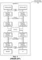
- FIG. 1 presents a block diagram illustrating a top view of an existing chip assembly configuration 100 that uses optical interconnects to facilitate communication among components (such as a processor, memory, a router, a switch, etc.).
- this chip assembly configuration has several disadvantages.
- the optical interconnects consume valuable real estate in the chip assembly configuration, which can increase cost.
- the distances between the components can increase, which can increase latency.
- thermal management of adjacent optical and electrical components in a chip assembly configuration can be difficult.
- US 2003/0038297 discloses an apparatus, system and method for transmission of information between microelectronic devices.
- WO 94/01987 discloses a component module comprised by at least one internal or external carrier substrate, at least one circuit with at least thereto belonging surrounding components or components.
- One embodiment of the present disclosure provides a chip assembly configuration that includes a substrate with a first surface and a second surface on an opposite side of the substrate from the first surface.
- the substrate also includes first connectors disposed on the first surface and second connectors disposed on the second surface, where the first connectors and the second connectors are electrically coupled by interconnectors through the substrate.
- a given interconnector includes two vias electrically coupled by a signal line that includes a region approximately parallel to one of the first surface and the second surface. These vias extend partially through the substrate. Furthermore, a length of the region is less than or equal to 1 mm.
- the chip assembly configuration includes an integrated circuit positioned adjacent to the first surface and electrically coupled to the first connectors.
- the chip assembly configuration includes a conversion mechanism positioned adjacent to the second surface and electrically coupled to the second connectors. This conversion mechanism converts electrical signals from the integrated circuit into corresponding first optical signals and converts second optical signals to the integrated circuit into corresponding second electrical signals. Note that the first optical signals and the second optical signals are communicated in the chip assembly configuration using an optical interconnect.
- the substrate may include: a printed circuit board and/or a interposer.
- the substrate may include: a semiconductor, an organic material, a ceramic, a glass, and/or a plastic.
- the chip assembly configuration includes sources and detectors optically coupled to the optical interconnect.
- the sources and detectors associated with the optical interconnect may be external to the chip assembly configuration.
- the optical interconnects may include: an optical fiber and/or an optical waveguide.
- first connectors and the integrated circuit may be electrically coupled by: solder, a ball-grid array, a socket, an interposer, and/or a land grid array.
- second connectors and the conversion mechanism may be electrically coupled by: solder, a ball-grid array, a socket, an interposer, and/or a land grid array.
- an average impedance of electrical paths associated with the first connectors, the second connectors and the interconnectors approximately matches an average impedance of drivers in the integrated circuit and the conversion mechanism.
- the average impedance may be approximately 50 ⁇ .
- a dominant pole in a transfer characteristic associated with the first connectors, the second connectors and the interconnectors may facilitate communication between the integrated circuit and the conversion mechanism at data rates greater than 10 Gbps.
- the chip assembly configuration may include a heat sink thermally coupled to the integrated circuit on an opposite side of the integrated circuit from the substrate.
- a given connector includes a straight-through via electrically coupled by signal lines from the first surface and second surface, wherein the via extends from the first surface to the second surface through the substrate.
- Another embodiment provides a system that includes the chip assembly configuration.
- This system may or may not include a processor and a memory.
- Another embodiment provides a method for communicating information in the chip assembly configuration.
- an electrical signal is driven from the integrated circuit in the electrical path through the substrate adjacent to the integrated circuit in the chip assembly configuration, wherein the electrical path includes the first connectors disposed on the first surface of the substrate, the second connectors disposed on the second surface of the substrate on the opposite side of the substrate from the first surface, and the interconnectors through the substrate that electrically couple the first connectors and the second connectors.
- a given interconnector includes two vias electrically coupled by a signal line that includes a region approximately parallel to one of the first surface and the second surface. These vias extend partially through the substrate. Furthermore, a length of the region is less than or equal to 1 mm.
- the electrical signal is received at the conversion mechanism positioned adjacent to the second surface and electrically coupled to the second connectors. Moreover, using the conversion mechanism, the electrical signal is converted to the optical signal. Next, the optical signal is communicated in the optical interconnect in the chip assembly configuration.
- Embodiments of a chip assembly configuration, a multi-chip module ( MCM ) that includes the chip assembly configuration, a system that includes the chip assembly configuration, and a technique for communicating information in the chip assembly configuration are described.
- This chip assembly configuration includes an substrate with an integrated circuit on one side and a conversion mechanism on the other side.
- the integrated circuit and the conversion mechanism are electrically coupled by a short electrical transmission line through the substrate.
- the conversion mechanism converts signals between an electrical and an optical domain, thereby allowing high-speed communication between the integrated circuit and other components and devices using optical communication (for example, in an optical fiber or an optical waveguide).
- the chip assembly configuration may address the challenges associated with lost real estate, latency, and thermal management, thereby allowing the use of dense configurations of optical I / O ports.
- the chip assembly configuration may allow the advantages associated with optical interconnects without the problems associated with existing implementations. Therefore, the chip assembly configuration may provide suitable communication and integration characteristics for use with next-generation multi-processor architectures in high-performance computer systems.
- FIG. 2 presents a block diagram illustrating a side view of a chip assembly configuration 200-1.
- This chip assembly configuration includes an substrate 210 (such as a printed-circuit board, a glass substrate, an inorganic substrate, a ceramic substrate, or a plastic substrate), having surfaces 212 on opposite sides of substrate 210, with connectors 214-1 disposed on surface 212-1 and connectors 214-2 disposed on surface 212-2. These connectors are electrically coupled by interconnectors 216 (such as transmission lines) through substrate 210. The combination of a given interconnector and a pair of connectors 214 may constitute an electrical path.
- substrate 210 such as a printed-circuit board, a glass substrate, an inorganic substrate, a ceramic substrate, or a plastic substrate
- interconnectors 216 such as transmission lines
- a given interconnector may include two vias 206 electrically coupled by a signal line 208 that includes a region 204 approximately parallel to one of surfaces 212 ( i.e ., which provides a short lateral hop). These vias may extend partially through substrate 210. Furthermore, a length of region 204 may be less than or equal to 1 mm, thereby facilitating high-speed communication with good signal integrity.
- a given connect may include a single via electrically coupled by signal lines straight from surface 212-1 to surface 212-2 or vice-versa.
- chip assembly configuration 200-1 includes an integrated circuit 218 positioned adjacent to surface 212-1 and electrically coupled to connectors 214-1 (for example, by solder and/or a ball-grid array). Furthermore, chip assembly configuration 200-1 includes conversion mechanisms 220 positioned adjacent to surface 212-2 and electrically coupled to connectors 214-2 (for example, by solder and/or a ball-grid array). These conversion mechanisms convert electrical signals from integrated circuit 218 into corresponding optical signals 222-1 and converts optical signals 222-2 to integrated circuit 218 into corresponding electrical signals. Note that optical signals 222 are communicated in chip assembly configuration 200-1 using one or more optical interconnects 224, such as: an optical fiber and/or an optical waveguide (such as an optical waveguide implemented using silicon-on-insulator technology).
- optical interconnects 224 such as: an optical fiber and/or an optical waveguide (such as an optical waveguide implemented using silicon-on-insulator technology).
- the chip assembly configuration includes optional sources 226 and/or optional detectors 228 that are optically coupled to the one or more optical interconnects 224.
- the sources and detectors associated with the one or more optical interconnects 224 may be external to chip assembly configuration 200-1.
- An average impedance of electrical paths associated with connectors 214-1, connectors 214-2 and interconnectors 216 may approximately match an average impedance of drivers in integrated circuit 218 and in one of conversion mechanisms 220.
- the average impedance may be 50 ⁇ with a large associated capacitance.
- a dominant pole in a transfer characteristic associated with connectors 214-1, connectors 214-2 and interconnectors 216 may facilitate communication between integrated circuit 218 and conversion mechanisms 220 at data rates greater than 10 Gbps.
- chip assembly configuration 200-1 may include an optional heat sink 230 thermally coupled to integrated circuit 218 on an opposite side of integrated circuit 218 from substrate 210. This may be useful because thermal stability is important for optical components. This configuration also frees up valuable real estate on surface 212-1, which can be used to reduce crosstalk and/or to increase the component density.
- each optical-channel driver or receiver I / O in a given one of conversion mechanisms 220 is electrically coupled to a corresponding high-speed driver/receiver pin on integrated circuit 218 (path #1).
- connections to power (path #2) and ground (path #3) are made.
- these connections may be enabled by two short vias (approximately 150-300 ⁇ m tall) and a small jog of an associated transmission line on the platform board layer (for example, less than 1 mm in length).
- This electrical hop may be the smallest electrical hop that can physically interconnect surfaces 212 (other than a through-via drop from surface 212-1 to surface 212-2, which may not be feasible for all connections).
- Such a small electrical connection may facilitate the highest data-rate signaling to and from serializer/deserializer I / O blocks in integrated circuit 218. For example, electrical crossovers and the signal degradation associated with the required additional vias can be avoided. In addition, the power requirements for I / O drivers may be reduced and/or the use of other communication techniques (such as pre-emphasis or equalization) may be reduced or eliminated.
- each optical I / O port in an optical subassembly in a given one of conversion mechanisms 220 can support 4, 8, 12 or 16 channels.
- Conversion mechanisms 220 may each be wide enough to support multiple channels (e.g ., 4, 8, 12, or 16 channels in 1- D or 2- D format) within a small footprint while still placing these optical I / O ports in close proximity to integrated circuits, such as integrated circuit 218.
- each lane may be either single-ended or differential.
- the optical I / O ports in the given one of conversion mechanisms 220 may include: a light source (such as a 1- D or 2- D vertical-cavity surface-emitting laser array that is operated in current or voltage mode), a detector (such as a 1- D or 2- D photodiode array, e.g ., a reverse-biased pn- junction diode, a pin diode, a metal-semiconductor-metal detector or a resonant-cavity enhanced detector) and associated drivers and receivers (such as a transimpedance amplifier and a limiting amplifier) in the form of electrical integrated circuits that can accommodate data rates up to 40 Gbps (which may be coupled to the optical components by an optical-fiber ribbon).
- the optical components may be implemented using III-V semiconductor compounds (such as GaAs or InP) as the base material.
- the optical components may be on the same substrate(s) as the electrical integrated circuits.
- the optical I / O ports in conversion mechanisms 220 may be physically attached to substrate 210 using: a reflow assembly process or remateable connections, such as an MEG-array® connector (from FCi, of Guyancourt, France) of micro-pin grid array ( ⁇ -PGA) connectors.
- optical connector/optical headers may be used to mate to the optical-fiber ribbons in optical interconnects 224 on standard MPO / MTP connectors (from Molex® Inc., of Lisle, IL) via passive alignment with respect to the individual transmit or receive channels.
- These optical headers may support space-division multiplexing (e.g ., a parallel channel of optical fibers) and/or wavelength-division multiplexing with suitable optical multiplexing/demultiplexing elements.
- conversion mechanisms 220 may be isolated from the heat generated by integrated circuit 218 during operation. At the same time, heat needs to be removed from the drivers and receivers in the electrical integrated circuits in conversion mechanisms 220. Otherwise, thermal roll-off may degrade the power of the light sources at elevated temperature. As a consequence, conversion mechanisms 220 may be thermally coupled to an optional heat sinks 232, such as a machined-aluminum or a copper block with fins.
- the tens of high-speed serializer/deserializer electrical I / O transmission lines can be eliminated.
- a typical processor includes serializer/deserializer I / O blocks on the perimeter of the chip, with differential transmission lines connected to the serializer/deserializer I / O pins.
- the number of differential pair lines required equals the bisection bandwidth divided by the maximum data rate per pin.
- the aggregate bandwidth to the processor needed is 2 Tbps (a bisection bandwidth of 4 Tbps) and each serializer/deserializer I / O pin supports 20 Gbps, then the number of pins or transmission lines needed is 2 Tbps divided by 20 Gbps, or 100. Multiplying by two for differential signaling yields 200 pins or transmission lines.
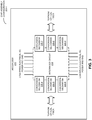
- FIG. 3 which presents a block diagram illustrating a bottom view of chip assembly configuration 200-1
- multiple arrays of optical assemblies in conversion mechanisms 220 can significantly reduce the number of pins or transmission lines.
- this configuration provides tighter integration of one or more processors and memory chips on the top surface of substrate 210, thereby removing or reducing routing congestion and improving signal integrity.
- chip assembly configuration 200-1 is a full-duplex implementation with transmit and receive channels in conversion mechanisms 220.
- the transmitter ( Tx ) and receiver ( Rx ) optical I / O port (or optical assemblies) in this configuration may be adjacent to each other (for example, in conversion mechanisms 220-1 and 220-2, respectively).
- this configuration may facilitate 2-16 channels.
- a half-duplex implementation is used with either transmit or receive channels in a given optical I / O port in a given conversion mechanism.
- transmitter and receiver optical assemblies in conversion mechanisms 220 may be physically separated and may be arranged in a wide variety of ways (e.g ., alternating Tx and Rx , Tx Tx Tx Tx followed by Rx Rx Rx Rx , etc.).
- the optical I / O ports on surface 212-2 of chip assembly configuration 200-1 can be arranged in several rows or in staggered rows. Physical space permits these arrangements because integrated circuit 218 does not block their paths and interconnectors 216 follow a vertical path through substrate 210. Note that, because interconnectors 216 follow this vertical path, serializer/deserializer I / O blocks may no longer be constrained to the perimeter of integrated circuit 218. As a consequence, a designer can choose to place the serializer/deserializer I / O blocks close to the processor chip perimeter and may eliminate corresponding vertical interconnect paths to a given conversion mechanism, such as conversion mechanism 220-1. Furthermore, some areas beneath the processor may be kept clear for bolster plates to mate the processor package to substrate 210.
- the optical I / O ports in conversion mechanisms 220 are based on vertical-cavity surface-emitting laser technology with wavelengths of 850, 1301 or 1550 nm and a corresponding GaAs or InP detector technology. Furthermore, the optical I / O ports in conversion mechanisms 220 may be based on a silicon-photonics technology that can support single-mode (i.e ., wavelength-division multiplexing) and/or multi-mode optical fibers ( i.e ., space-division multiplexing) using a reduced number of distributed-feedback laser arrays.
- single-mode i.e ., wavelength-division multiplexing
- multi-mode optical fibers i.e ., space-division multiplexing
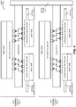
- FIG. 4 presents a block diagram illustrating a side view of a multi-chip module MCM 400 with chip assembly configurations 200 connected to a backplane 410. Note that with the arrangement of the optical I / O ports in conversion mechanisms on the bottom sides of the substrates, bulky copper cables may be replaced with thin optical-fiber ribbons, which can all be aggregated into a high-density, compact, optical-fiber-connector patch panel.
- This configuration may allow the optical signals to be redistributed internally and/or externally to MCM 400 using electrical and/or optical switches. Moreover, this configuration may allow unconstrained air flow between the substrates, both for the integrated circuits and the conversion mechanisms. Furthermore, by removing bulky copper cables, additional cable-management support harnesses may not be needed. (Thus, chip assembly configurations 200 may provide enhanced reliability.) In addition, the optical I / O ports in the conversion mechanisms can be arranged directly below the other chips, as well as switches, memory, etc., thereby reducing the length of electrical signal lines to these components.
- the chip assembly configuration may be used in a variety of applications. This is shown in FIG. 5 , which presents a block diagram illustrating a system 500 that includes a chip assembly configuration 508, such as chip assembly configuration 200-1 ( FIG. 2 ).
- Optical interconnects 506 on or optically coupled to conversion mechanisms in chip assembly configuration 508 may couple one or more processors 510, memory 524 and/or a communication interface 512.
- one or more processors 510 may be coupled to user interface 514 by one or more signal lines 522.
- the one or more processors (or processor cores) 510 may support parallel processing and/or multi-threaded operation
- the communication interface 512 may have a persistent communication connection
- the one or more signal lines 522 may constitute a communication bus.
- the user interface 514 may include: a display 516, a keyboard 518, and/or a pointer 520, such as a mouse.
- Memory 524 in system 500 may include volatile memory and/or non-volatile memory. More specifically, memory 524 may include: ROM , RAM , EPROM , EEPROM , flash, one or more smart cards, one or more magnetic disc storage devices, and/or one or more optical storage devices. Memory 524 may store an operating system 526 that includes procedures (or a set of instructions) for handling various basic system services for performing hardware-dependent tasks. Moreover, memory 524 may also store communications procedures (or a set of instructions) in a communication module 528. These communication procedures may be used for communicating with one or more computers, devices and/or servers, including computers, devices and/or servers that are remotely located with respect to the system 500.
- Memory 524 may also include one or more program modules 530 (or a set of instructions). Note that one or more of program modules 530 may constitute a computer-program mechanism. Instructions in the various modules in the memory 524 may be implemented in: a high-level procedural language, an object-oriented programming language, and/or in an assembly or machine language. The programming language may be compiled or interpreted, i.e ., configurable or configured, to be executed by the one or more processors (or processor cores) 510.
- System 500 may include: a VLSI circuit, a switch, a hub, a bridge, a router, a communication system (such as in wavelength division multiplexing), a storage area network, a data center, a network (such as a local area network), and/or a computer system (such as a multiple-core processor computer system).
- the chip assembly configuration may be included in a backplane that is coupled to multiple processor blades or, as shown in FIG. 4 , in an MCM that couples different types of components (such as processors, memory, I / O devices, and/or peripheral devices).
- this MCM performs the functions of: a switch, a hub, a bridge, and/or a router.
- the computer system may include, but is not limited to: a server (such as a multi-socket, multi-rack server), a laptop computer, a communication device or system, a personal computer, a work station, a mainframe computer, a blade, an enterprise computer, a data center, a portable-computing device, a tablet, a supercomputer, a network-attached-storage (NAS ) system, a storage-area-network (SAN ) system, and/or another electronic computing device.
- a server such as a multi-socket, multi-rack server
- a laptop computer such as a multi-socket, multi-rack server
- a communication device or system such as a personal computer, a work station, a mainframe computer, a blade, an enterprise computer, a data center, a portable-computing device, a tablet, a supercomputer, a network-attached-storage (NAS ) system, a storage-area-network (SAN
- system 500 may be at one location or may be distributed over multiple, geographically dispersed locations. Moreover, some or all of the functionality of system 500 may be implemented in one or more application-specific integrated circuits ( ASICs ) and/or one or more digital signal processors ( DSPs ). Furthermore, functionality in the preceding embodiments may be implemented more in hardware and less in software, or less in hardware and more in software, as is known in the art.
- ASICs application-specific integrated circuits
- DSPs digital signal processors
- the preceding embodiments may include fewer components or additional components.
- the chip assembly configuration and system are illustrated as having a number of discrete items, these embodiments are intended to be functional descriptions of the various features that may be present rather than structural schematics of the embodiments described herein. Consequently, in these embodiments, two or more components may be combined into a single component and/or a position of one or more components may be changed. Furthermore, features in two or more of the preceding embodiments may be combined with one another.
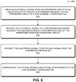
- FIG. 6 presents a flow diagram illustrating a method 600 for communicating information in a chip assembly configuration, which may be chip assembly configuration 200-1 ( FIG. 2 ).
- an electrical signal is driven from an integrated circuit in an electrical path through an substrate adjacent to the integrated circuit in the chip assembly configuration (operation 610), wherein the electrical path includes first connectors disposed on a first surface of the substrate, second connectors disposed on a second surface of the substrate on an opposite side of the substrate from the first surface, and interconnectors through the substrate that electrically couple the first connectors and the second connectors.
- the electrical signal is received at a conversion mechanism positioned adjacent to the second surface and electrically coupled to the second connectors (operation 612).
- the electrical signal is converted to an optical signal (operation 614).
- the optical signal is communicated in an optical interconnect in the chip assembly configuration (operation 616).
- method 600 includes additional or fewer operations. Moreover, the order of the operations may be changed, and/or two or more operations may be combined into a single operation.
Applications Claiming Priority (2)
| Application Number | Priority Date | Filing Date | Title |
|---|---|---|---|
| US13/410,113 US20130230272A1 (en) | 2012-03-01 | 2012-03-01 | Chip assembly configuration with densely packed optical interconnects |
| PCT/US2013/028355 WO2013130831A2 (en) | 2012-03-01 | 2013-02-28 | Chip assembly configuration with densely packed optical interconnects |
Publications (2)
| Publication Number | Publication Date |
|---|---|
| EP2820461A2 EP2820461A2 (en) | 2015-01-07 |
| EP2820461B1 true EP2820461B1 (en) | 2020-04-08 |
Family
ID=47915320
Family Applications (1)
| Application Number | Title | Priority Date | Filing Date |
|---|---|---|---|
| EP13711491.4A Active EP2820461B1 (en) | 2012-03-01 | 2013-02-28 | Chip assembly configuration with densely packed optical interconnects |
Country Status (6)
| Country | Link |
|---|---|
| US (1) | US20130230272A1 (ja) |
| EP (1) | EP2820461B1 (ja) |
| JP (1) | JP6294838B2 (ja) |
| CN (1) | CN104395801B (ja) |
| TW (1) | TWI598647B (ja) |
| WO (1) | WO2013130831A2 (ja) |
Families Citing this family (38)
| Publication number | Priority date | Publication date | Assignee | Title |
|---|---|---|---|---|
| US9874688B2 (en) | 2012-04-26 | 2018-01-23 | Acacia Communications, Inc. | Co-packaging photonic integrated circuits and application specific integrated circuits |
| US10446700B2 (en) * | 2013-05-22 | 2019-10-15 | W&Wsens Devices, Inc. | Microstructure enhanced absorption photosensitive devices |
| US10468543B2 (en) | 2013-05-22 | 2019-11-05 | W&Wsens Devices, Inc. | Microstructure enhanced absorption photosensitive devices |
| WO2014190189A2 (en) | 2013-05-22 | 2014-11-27 | Shih-Yuan Wang | Microstructure enhanced absorption photosensitive devices |
| US11121271B2 (en) | 2013-05-22 | 2021-09-14 | W&WSens, Devices, Inc. | Microstructure enhanced absorption photosensitive devices |
| US10700225B2 (en) | 2013-05-22 | 2020-06-30 | W&Wsens Devices, Inc. | Microstructure enhanced absorption photosensitive devices |
| US9496248B2 (en) * | 2014-01-06 | 2016-11-15 | Fujitsu Limited | Interposer for integrated circuit chip package |
| US9671572B2 (en) * | 2014-09-22 | 2017-06-06 | Oracle International Corporation | Integrated chip package with optical interface |
| SG11201703131WA (en) | 2014-10-29 | 2017-05-30 | Acacia Communications Inc | Optoelectronic ball grid array package with fiber |
| US9678271B2 (en) * | 2015-01-26 | 2017-06-13 | Oracle International Corporation | Packaged opto-electronic module |
| WO2017019025A1 (en) | 2015-07-27 | 2017-02-02 | Hewlett Packard Enterprise Development Lp | Socket to support boards in a spaced relation |
| CN107534029B (zh) * | 2015-07-31 | 2021-11-26 | 慧与发展有限责任合伙企业 | 多芯片模块 |
| US10031177B2 (en) | 2015-08-18 | 2018-07-24 | Juniper Networks, Inc. | Methods and apparatus for optical transceiver calibration and test |
| US10234626B2 (en) * | 2016-02-08 | 2019-03-19 | Skorpios Technologies, Inc. | Stepped optical bridge for connecting semiconductor waveguides |
| US10509163B2 (en) | 2016-02-08 | 2019-12-17 | Skorpios Technologies, Inc. | High-speed optical transmitter with a silicon substrate |
| US10732349B2 (en) | 2016-02-08 | 2020-08-04 | Skorpios Technologies, Inc. | Broadband back mirror for a III-V chip in silicon photonics |
| CN105608298B (zh) * | 2016-03-03 | 2019-07-16 | 深圳市紫光同创电子有限公司 | 一种基于阵列封装的fpga芯片 |
| US9900974B2 (en) * | 2016-06-02 | 2018-02-20 | Finisar Corporation | Flex-less multilayer ceramic substrate |
| US10034407B2 (en) * | 2016-07-22 | 2018-07-24 | Intel Corporation | Storage sled for a data center |
| US11531174B2 (en) | 2017-09-28 | 2022-12-20 | Intel Corporation | Co-packaging with silicon photonics hybrid planar lightwave circuit |
| US10928588B2 (en) | 2017-10-13 | 2021-02-23 | Skorpios Technologies, Inc. | Transceiver module for optical communication |
| US11573387B2 (en) * | 2018-04-12 | 2023-02-07 | Rockley Photonics Limited | Optical engine |
| GB2587961B (en) | 2018-04-12 | 2022-05-18 | Rockley Photonics Ltd | Electro-optical package and method of fabrication |
| GB2587962B (en) * | 2018-04-12 | 2022-12-14 | Rockley Photonics Ltd | Optical engine |
| US10716213B2 (en) | 2018-07-28 | 2020-07-14 | Hewlett Packard Enterprise Development Lp | Direct connection of high speed signals on PCB chip |
| US10517167B1 (en) | 2018-10-19 | 2019-12-24 | Eagle Technology, Llc | Systems and methods for providing a high speed interconnect system with reduced crosstalk |
| US10928585B2 (en) | 2018-10-26 | 2021-02-23 | Micron Technology, Inc. | Semiconductor devices having electro-optical substrates |
| US11024617B2 (en) * | 2018-10-26 | 2021-06-01 | Micron Technology, Inc. | Semiconductor packages having photon integrated circuit (PIC) chips |
| US20210398961A1 (en) * | 2018-12-03 | 2021-12-23 | Aayuna Inc. | High Density Optical Interconnection Assembly |
| GB2597179B (en) * | 2019-04-04 | 2023-07-05 | Rockley Photonics Ltd | Optical engine |
| US11056850B2 (en) | 2019-07-26 | 2021-07-06 | Eagle Technology, Llc | Systems and methods for providing a soldered interface on a printed circuit board having a blind feature |
| US11602800B2 (en) | 2019-10-10 | 2023-03-14 | Eagle Technology, Llc | Systems and methods for providing an interface on a printed circuit board using pin solder enhancement |
| US11256049B2 (en) * | 2020-04-22 | 2022-02-22 | Nokia Solutions And Networks Oy | Optical-to-electric-to-optical routing engine |
| US11437323B2 (en) | 2020-06-03 | 2022-09-06 | Hewlett Packard Enterprise Development Lp | Silicon interposer for capacitive coupling of photodiode arrays |
| US11283204B1 (en) | 2020-11-19 | 2022-03-22 | Eagle Technology, Llc | Systems and methods for providing a composite connector for high speed interconnect systems |
| US11929357B2 (en) | 2021-10-20 | 2024-03-12 | Advanced Semiconductor Engineering, Inc. | Optoelectronic package structure and method of manufacturing the same |
| CN113917631B (zh) * | 2021-10-20 | 2024-03-01 | 东莞立讯技术有限公司 | 共封装集成光电模块及共封装光电交换芯片结构 |
| CN116299887A (zh) * | 2021-12-14 | 2023-06-23 | 上海曦智科技有限公司 | 光互连装置及其制造方法、计算装置 |
Family Cites Families (25)
| Publication number | Priority date | Publication date | Assignee | Title |
|---|---|---|---|---|
| SE9202077L (sv) * | 1992-07-06 | 1994-01-07 | Ellemtel Utvecklings Ab | Komponentmodul |
| JP2002050821A (ja) * | 2000-07-31 | 2002-02-15 | Kyocera Corp | 光実装基板及びそれを用いた光モジュール |
| JP2002261265A (ja) * | 2001-03-06 | 2002-09-13 | Sumitomo Electric Ind Ltd | 光通信装置 |
| US20030038297A1 (en) * | 2001-07-24 | 2003-02-27 | Robert Carroll | Apparatus,system, and method for transmission of information between microelectronic devices |
| US6752539B2 (en) * | 2002-06-28 | 2004-06-22 | International Buisness Machines Corporation | Apparatus and system for providing optical bus interprocessor interconnection |
| US7327022B2 (en) * | 2002-12-30 | 2008-02-05 | General Electric Company | Assembly, contact and coupling interconnection for optoelectronics |
| US7128472B2 (en) * | 2003-07-31 | 2006-10-31 | International Business Machines Corporation | Method and apparatus for providing optoelectronic communication with an electronic device |
| JP2005085844A (ja) * | 2003-09-05 | 2005-03-31 | Ngk Spark Plug Co Ltd | 光電気複合配線構造体及びその製造方法 |
| JP2005159060A (ja) * | 2003-11-26 | 2005-06-16 | Kyocera Corp | 同軸型半導体レーザモジュール |
| US7058247B2 (en) * | 2003-12-17 | 2006-06-06 | International Business Machines Corporation | Silicon carrier for optical interconnect modules |
| US7657185B2 (en) * | 2004-01-26 | 2010-02-02 | Opnext, Inc. | Electronic interface for long reach optical transceiver |
| JP4138689B2 (ja) * | 2004-03-30 | 2008-08-27 | 株式会社東芝 | インターフェイスモジュール付lsiパッケージ及びlsiパッケージ |
| JP2006259682A (ja) * | 2005-02-18 | 2006-09-28 | Sony Corp | 光電複合装置、それに用いられるicソケットおよび光導波路、光導波路結合チップ、並びにそれを用いた電子機器 |
| JP2007057972A (ja) * | 2005-08-25 | 2007-03-08 | Nec Electronics Corp | 光モジュール |
| WO2007114384A1 (ja) * | 2006-04-03 | 2007-10-11 | The University Of Tokyo | 信号伝送機器 |
| CN101506705B (zh) * | 2006-09-21 | 2011-07-06 | 日立化成工业株式会社 | 光波导基片及使用其的光电混载电路安装基片 |
| US7891924B2 (en) * | 2006-11-03 | 2011-02-22 | Huck International, Inc. | Low swage load fastening system and method |
| US7329054B1 (en) * | 2007-03-05 | 2008-02-12 | Aprius, Inc. | Optical transceiver for computing applications |
| JP4895957B2 (ja) * | 2007-09-25 | 2012-03-14 | 日本特殊陶業株式会社 | 光電気混載パッケージ、光電気混載モジュール |
| CN101932963A (zh) * | 2008-01-30 | 2010-12-29 | 惠普发展公司,有限责任合伙企业 | 光学互连 |
| US8422837B2 (en) * | 2008-02-28 | 2013-04-16 | Nec Corporation | Semiconductor device |
| US9112616B2 (en) * | 2008-08-13 | 2015-08-18 | Avago Technologies General Ip (Singapore) Pte. Ltd. | Transceiver system on a card for simultaneously transmitting and receiving information at a rate equal to or greater than approximately one terabit per second |
| JP5102815B2 (ja) * | 2009-08-31 | 2012-12-19 | 日立電線株式会社 | 光電気複合配線モジュールおよびその製造方法 |
| JP5300700B2 (ja) * | 2009-11-28 | 2013-09-25 | 京セラ株式会社 | 光配線基板 |
| JP2011248243A (ja) * | 2010-05-28 | 2011-12-08 | Fujitsu Component Ltd | 光電変換モジュール及び光電変換装置 |
-
2012
- 2012-03-01 US US13/410,113 patent/US20130230272A1/en not_active Abandoned
-
2013
- 2013-02-21 TW TW102106022A patent/TWI598647B/zh active
- 2013-02-28 EP EP13711491.4A patent/EP2820461B1/en active Active
- 2013-02-28 WO PCT/US2013/028355 patent/WO2013130831A2/en active Application Filing
- 2013-02-28 CN CN201380011906.7A patent/CN104395801B/zh active Active
- 2013-02-28 JP JP2014560046A patent/JP6294838B2/ja active Active
Non-Patent Citations (1)
| Title |
|---|
| None * |
Also Published As
| Publication number | Publication date |
|---|---|
| US20130230272A1 (en) | 2013-09-05 |
| TW201400894A (zh) | 2014-01-01 |
| CN104395801A (zh) | 2015-03-04 |
| JP6294838B2 (ja) | 2018-03-14 |
| TWI598647B (zh) | 2017-09-11 |
| JP2015511027A (ja) | 2015-04-13 |
| EP2820461A2 (en) | 2015-01-07 |
| WO2013130831A2 (en) | 2013-09-06 |
| WO2013130831A3 (en) | 2013-12-27 |
| CN104395801B (zh) | 2017-03-01 |
Similar Documents
| Publication | Publication Date | Title |
|---|---|---|
| EP2820461B1 (en) | Chip assembly configuration with densely packed optical interconnects | |
| US9671572B2 (en) | Integrated chip package with optical interface | |
| US8998509B2 (en) | Stackable photonic interconnect module | |
| US11424837B2 (en) | Method and system for large silicon photonic interposers by stitching | |
| US11178473B1 (en) | Co-packaged light engine chiplets on switch substrate | |
| Benner et al. | Exploitation of optical interconnects in future server architectures | |
| US11612079B2 (en) | Heatsink for co-packaged optical switch rack package | |
| Schow et al. | Get on the optical bus | |
| US11677478B2 (en) | Method for co-packaging light engine chiplets on switch substrate | |
| US20200057218A1 (en) | Photonics package integration | |
| Li et al. | Transferring high-speed data over long distances with combined FPGA and multichannel optical modules | |
| US20230299854A1 (en) | Hybrid integration of microled interconnects with ics | |
| JP7144786B2 (ja) | 小型光トランシーバ | |
| US20030038297A1 (en) | Apparatus,system, and method for transmission of information between microelectronic devices | |
| Tanaka et al. | High-bandwidth optical interconnect technologies for next-generation server systems | |
| Taira | Technology for optical co-packaging | |
| US20240036254A1 (en) | High-capacity optical input/output for data processors | |
| US20240097796A1 (en) | Photonic chiplet packaging | |
| Kash | Optical/electrical technologies for high speed signal communications in high performance servers | |
| Evans-Pughe | Charge of the light brigade [photonics] | |
| CN108519644A (zh) | Aoc光模块 | |
| Krishnamoorthy et al. | Delivering On-chip Bandwidth Off-chip and Out-of-box with Proximity and Optical Communication |
Legal Events
| Date | Code | Title | Description |
|---|---|---|---|
| PUAI | Public reference made under article 153(3) epc to a published international application that has entered the european phase |
Free format text: ORIGINAL CODE: 0009012 |
|
| 17P | Request for examination filed |
Effective date: 20140825 |
|
| AK | Designated contracting states |
Kind code of ref document: A2 Designated state(s): AL AT BE BG CH CY CZ DE DK EE ES FI FR GB GR HR HU IE IS IT LI LT LU LV MC MK MT NL NO PL PT RO RS SE SI SK SM TR |
|
| AX | Request for extension of the european patent |
Extension state: BA ME |
|
| DAX | Request for extension of the european patent (deleted) | ||
| GRAP | Despatch of communication of intention to grant a patent |
Free format text: ORIGINAL CODE: EPIDOSNIGR1 |
|
| STAA | Information on the status of an ep patent application or granted ep patent |
Free format text: STATUS: GRANT OF PATENT IS INTENDED |
|
| INTG | Intention to grant announced |
Effective date: 20191112 |
|
| GRAS | Grant fee paid |
Free format text: ORIGINAL CODE: EPIDOSNIGR3 |
|
| GRAA | (expected) grant |
Free format text: ORIGINAL CODE: 0009210 |
|
| STAA | Information on the status of an ep patent application or granted ep patent |
Free format text: STATUS: THE PATENT HAS BEEN GRANTED |
|
| AK | Designated contracting states |
Kind code of ref document: B1 Designated state(s): AL AT BE BG CH CY CZ DE DK EE ES FI FR GB GR HR HU IE IS IT LI LT LU LV MC MK MT NL NO PL PT RO RS SE SI SK SM TR |
|
| REG | Reference to a national code |
Ref country code: AT Ref legal event code: REF Ref document number: 1255162 Country of ref document: AT Kind code of ref document: T Effective date: 20200415 Ref country code: CH Ref legal event code: EP |
|
| REG | Reference to a national code |
Ref country code: IE Ref legal event code: FG4D |
|
| REG | Reference to a national code |
Ref country code: DE Ref legal event code: R096 Ref document number: 602013067656 Country of ref document: DE |
|
| REG | Reference to a national code |
Ref country code: NL Ref legal event code: MP Effective date: 20200408 |
|
| REG | Reference to a national code |
Ref country code: LT Ref legal event code: MG4D |
|
| PG25 | Lapsed in a contracting state [announced via postgrant information from national office to epo] |
Ref country code: NL Free format text: LAPSE BECAUSE OF FAILURE TO SUBMIT A TRANSLATION OF THE DESCRIPTION OR TO PAY THE FEE WITHIN THE PRESCRIBED TIME-LIMIT Effective date: 20200408 Ref country code: SE Free format text: LAPSE BECAUSE OF FAILURE TO SUBMIT A TRANSLATION OF THE DESCRIPTION OR TO PAY THE FEE WITHIN THE PRESCRIBED TIME-LIMIT Effective date: 20200408 Ref country code: GR Free format text: LAPSE BECAUSE OF FAILURE TO SUBMIT A TRANSLATION OF THE DESCRIPTION OR TO PAY THE FEE WITHIN THE PRESCRIBED TIME-LIMIT Effective date: 20200709 Ref country code: LT Free format text: LAPSE BECAUSE OF FAILURE TO SUBMIT A TRANSLATION OF THE DESCRIPTION OR TO PAY THE FEE WITHIN THE PRESCRIBED TIME-LIMIT Effective date: 20200408 Ref country code: FI Free format text: LAPSE BECAUSE OF FAILURE TO SUBMIT A TRANSLATION OF THE DESCRIPTION OR TO PAY THE FEE WITHIN THE PRESCRIBED TIME-LIMIT Effective date: 20200408 Ref country code: IS Free format text: LAPSE BECAUSE OF FAILURE TO SUBMIT A TRANSLATION OF THE DESCRIPTION OR TO PAY THE FEE WITHIN THE PRESCRIBED TIME-LIMIT Effective date: 20200808 Ref country code: NO Free format text: LAPSE BECAUSE OF FAILURE TO SUBMIT A TRANSLATION OF THE DESCRIPTION OR TO PAY THE FEE WITHIN THE PRESCRIBED TIME-LIMIT Effective date: 20200708 Ref country code: PT Free format text: LAPSE BECAUSE OF FAILURE TO SUBMIT A TRANSLATION OF THE DESCRIPTION OR TO PAY THE FEE WITHIN THE PRESCRIBED TIME-LIMIT Effective date: 20200817 |
|
| REG | Reference to a national code |
Ref country code: AT Ref legal event code: MK05 Ref document number: 1255162 Country of ref document: AT Kind code of ref document: T Effective date: 20200408 |
|
| PG25 | Lapsed in a contracting state [announced via postgrant information from national office to epo] |
Ref country code: RS Free format text: LAPSE BECAUSE OF FAILURE TO SUBMIT A TRANSLATION OF THE DESCRIPTION OR TO PAY THE FEE WITHIN THE PRESCRIBED TIME-LIMIT Effective date: 20200408 Ref country code: HR Free format text: LAPSE BECAUSE OF FAILURE TO SUBMIT A TRANSLATION OF THE DESCRIPTION OR TO PAY THE FEE WITHIN THE PRESCRIBED TIME-LIMIT Effective date: 20200408 Ref country code: LV Free format text: LAPSE BECAUSE OF FAILURE TO SUBMIT A TRANSLATION OF THE DESCRIPTION OR TO PAY THE FEE WITHIN THE PRESCRIBED TIME-LIMIT Effective date: 20200408 Ref country code: BG Free format text: LAPSE BECAUSE OF FAILURE TO SUBMIT A TRANSLATION OF THE DESCRIPTION OR TO PAY THE FEE WITHIN THE PRESCRIBED TIME-LIMIT Effective date: 20200708 |
|
| PG25 | Lapsed in a contracting state [announced via postgrant information from national office to epo] |
Ref country code: AL Free format text: LAPSE BECAUSE OF FAILURE TO SUBMIT A TRANSLATION OF THE DESCRIPTION OR TO PAY THE FEE WITHIN THE PRESCRIBED TIME-LIMIT Effective date: 20200408 |
|
| REG | Reference to a national code |
Ref country code: DE Ref legal event code: R097 Ref document number: 602013067656 Country of ref document: DE |
|
| PG25 | Lapsed in a contracting state [announced via postgrant information from national office to epo] |
Ref country code: AT Free format text: LAPSE BECAUSE OF FAILURE TO SUBMIT A TRANSLATION OF THE DESCRIPTION OR TO PAY THE FEE WITHIN THE PRESCRIBED TIME-LIMIT Effective date: 20200408 Ref country code: SM Free format text: LAPSE BECAUSE OF FAILURE TO SUBMIT A TRANSLATION OF THE DESCRIPTION OR TO PAY THE FEE WITHIN THE PRESCRIBED TIME-LIMIT Effective date: 20200408 Ref country code: EE Free format text: LAPSE BECAUSE OF FAILURE TO SUBMIT A TRANSLATION OF THE DESCRIPTION OR TO PAY THE FEE WITHIN THE PRESCRIBED TIME-LIMIT Effective date: 20200408 Ref country code: CZ Free format text: LAPSE BECAUSE OF FAILURE TO SUBMIT A TRANSLATION OF THE DESCRIPTION OR TO PAY THE FEE WITHIN THE PRESCRIBED TIME-LIMIT Effective date: 20200408 Ref country code: RO Free format text: LAPSE BECAUSE OF FAILURE TO SUBMIT A TRANSLATION OF THE DESCRIPTION OR TO PAY THE FEE WITHIN THE PRESCRIBED TIME-LIMIT Effective date: 20200408 Ref country code: IT Free format text: LAPSE BECAUSE OF FAILURE TO SUBMIT A TRANSLATION OF THE DESCRIPTION OR TO PAY THE FEE WITHIN THE PRESCRIBED TIME-LIMIT Effective date: 20200408 Ref country code: ES Free format text: LAPSE BECAUSE OF FAILURE TO SUBMIT A TRANSLATION OF THE DESCRIPTION OR TO PAY THE FEE WITHIN THE PRESCRIBED TIME-LIMIT Effective date: 20200408 Ref country code: DK Free format text: LAPSE BECAUSE OF FAILURE TO SUBMIT A TRANSLATION OF THE DESCRIPTION OR TO PAY THE FEE WITHIN THE PRESCRIBED TIME-LIMIT Effective date: 20200408 |
|
| PLBE | No opposition filed within time limit |
Free format text: ORIGINAL CODE: 0009261 |
|
| STAA | Information on the status of an ep patent application or granted ep patent |
Free format text: STATUS: NO OPPOSITION FILED WITHIN TIME LIMIT |
|
| PG25 | Lapsed in a contracting state [announced via postgrant information from national office to epo] |
Ref country code: SK Free format text: LAPSE BECAUSE OF FAILURE TO SUBMIT A TRANSLATION OF THE DESCRIPTION OR TO PAY THE FEE WITHIN THE PRESCRIBED TIME-LIMIT Effective date: 20200408 Ref country code: PL Free format text: LAPSE BECAUSE OF FAILURE TO SUBMIT A TRANSLATION OF THE DESCRIPTION OR TO PAY THE FEE WITHIN THE PRESCRIBED TIME-LIMIT Effective date: 20200408 |
|
| 26N | No opposition filed |
Effective date: 20210112 |
|
| PG25 | Lapsed in a contracting state [announced via postgrant information from national office to epo] |
Ref country code: SI Free format text: LAPSE BECAUSE OF FAILURE TO SUBMIT A TRANSLATION OF THE DESCRIPTION OR TO PAY THE FEE WITHIN THE PRESCRIBED TIME-LIMIT Effective date: 20200408 |
|
| PG25 | Lapsed in a contracting state [announced via postgrant information from national office to epo] |
Ref country code: MC Free format text: LAPSE BECAUSE OF FAILURE TO SUBMIT A TRANSLATION OF THE DESCRIPTION OR TO PAY THE FEE WITHIN THE PRESCRIBED TIME-LIMIT Effective date: 20200408 |
|
| REG | Reference to a national code |
Ref country code: BE Ref legal event code: MM Effective date: 20210228 |
|
| PG25 | Lapsed in a contracting state [announced via postgrant information from national office to epo] |
Ref country code: CH Free format text: LAPSE BECAUSE OF NON-PAYMENT OF DUE FEES Effective date: 20210228 Ref country code: LU Free format text: LAPSE BECAUSE OF NON-PAYMENT OF DUE FEES Effective date: 20210228 Ref country code: LI Free format text: LAPSE BECAUSE OF NON-PAYMENT OF DUE FEES Effective date: 20210228 |
|
| PG25 | Lapsed in a contracting state [announced via postgrant information from national office to epo] |
Ref country code: FR Free format text: LAPSE BECAUSE OF NON-PAYMENT OF DUE FEES Effective date: 20210228 Ref country code: IE Free format text: LAPSE BECAUSE OF NON-PAYMENT OF DUE FEES Effective date: 20210228 |
|
| PG25 | Lapsed in a contracting state [announced via postgrant information from national office to epo] |
Ref country code: BE Free format text: LAPSE BECAUSE OF NON-PAYMENT OF DUE FEES Effective date: 20210228 |
|
| PG25 | Lapsed in a contracting state [announced via postgrant information from national office to epo] |
Ref country code: HU Free format text: LAPSE BECAUSE OF FAILURE TO SUBMIT A TRANSLATION OF THE DESCRIPTION OR TO PAY THE FEE WITHIN THE PRESCRIBED TIME-LIMIT; INVALID AB INITIO Effective date: 20130228 |
|
| P01 | Opt-out of the competence of the unified patent court (upc) registered |
Effective date: 20230522 |
|
| PG25 | Lapsed in a contracting state [announced via postgrant information from national office to epo] |
Ref country code: CY Free format text: LAPSE BECAUSE OF FAILURE TO SUBMIT A TRANSLATION OF THE DESCRIPTION OR TO PAY THE FEE WITHIN THE PRESCRIBED TIME-LIMIT Effective date: 20200408 |
|
| PG25 | Lapsed in a contracting state [announced via postgrant information from national office to epo] |
Ref country code: MK Free format text: LAPSE BECAUSE OF FAILURE TO SUBMIT A TRANSLATION OF THE DESCRIPTION OR TO PAY THE FEE WITHIN THE PRESCRIBED TIME-LIMIT Effective date: 20200408 |
|
| PGFP | Annual fee paid to national office [announced via postgrant information from national office to epo] |
Ref country code: DE Payment date: 20231229 Year of fee payment: 12 Ref country code: GB Payment date: 20240108 Year of fee payment: 12 |