EP2797236A2 - Zeitkontinuierlicher Delta-Sigma-Modulator - Google Patents
Zeitkontinuierlicher Delta-Sigma-Modulator Download PDFInfo
- Publication number
- EP2797236A2 EP2797236A2 EP14001368.1A EP14001368A EP2797236A2 EP 2797236 A2 EP2797236 A2 EP 2797236A2 EP 14001368 A EP14001368 A EP 14001368A EP 2797236 A2 EP2797236 A2 EP 2797236A2
- Authority
- EP
- European Patent Office
- Prior art keywords
- resistor
- comp
- clk
- sigma modulator
- time
- Prior art date
- Legal status (The legal status is an assumption and is not a legal conclusion. Google has not performed a legal analysis and makes no representation as to the accuracy of the status listed.)
- Granted
Links
Images

Classifications
-
- H—ELECTRICITY
- H03—ELECTRONIC CIRCUITRY
- H03M—CODING; DECODING; CODE CONVERSION IN GENERAL
- H03M3/00—Conversion of analogue values to or from differential modulation
- H03M3/30—Delta-sigma modulation
-
- H—ELECTRICITY
- H03—ELECTRONIC CIRCUITRY
- H03M—CODING; DECODING; CODE CONVERSION IN GENERAL
- H03M3/00—Conversion of analogue values to or from differential modulation
- H03M3/30—Delta-sigma modulation
- H03M3/322—Continuously compensating for, or preventing, undesired influence of physical parameters
-
- H—ELECTRICITY
- H03—ELECTRONIC CIRCUITRY
- H03M—CODING; DECODING; CODE CONVERSION IN GENERAL
- H03M3/00—Conversion of analogue values to or from differential modulation
- H03M3/30—Delta-sigma modulation
- H03M3/458—Analogue/digital converters using delta-sigma modulation as an intermediate step
Definitions
- the present invention relates to a time-continuous delta-sigma modulator.
- composite semiconductor devices are fabricated in a field of identical (semiconductor) elements distributed on a wafer about a common center of gravity to compensate for potential gradients of inhomogeneities in process parameters (layer thicknesses, doping, etc.) resulting from process tolerances along the process Surface yield.
- process parameters layer thicknesses, doping, etc.
- the object of the invention is to improve as far as possible a time-continuous delta-sigma modulator, in particular as part of an analog-to-digital converter.
- the time-continuous delta-sigma modulator has an integrator and a comparator clocked with a clock frequency by means of a clock signal.
- the integrator and the comparator are connected in a feedback loop.
- the time-continuous delta-sigma modulator has a voltage source.
- the voltage source is connected to the comparator for applying a threshold voltage to the comparator.
- An integration time constant of the integrator includes a first resistor and a first capacitor.
- the voltage source has a second resistor and a second capacitance for adjusting the threshold voltage.
- the first resistor and the second resistor are part of a resistor pairing structure.
- the first capacity and the second capacity are part of a capacity pairing structure.
- the resistive pairing structure can be achieved on a semiconductor chip by making the first resistor and the second resistor by the same process steps.
- the first resistor and the second resistor are disposed on the semiconductor chip so as to be electrically isolated from one another.
- the capacitance pairing structure can be achieved on the semiconductor chip by manufacturing the first capacitance and the second capacitance by the same process steps.
- the first capacitance and the second capacitance are arranged on the semiconductor chip in an electrically insulated manner adjacent to one another.
- the stability of the loop gain of the time-continuous delta-sigma modulator is achieved for a wide range of clock frequencies. Furthermore, no measurement process and associated dimensioning of a control is required.
- the threshold voltage is not regulated by the voltage source, but controlled, which allows a very rapid adjustment of the threshold voltage. Influences of temperature changes and production-related deviations are largely reduced.
- the comparator is designed to change a loop gain of the feedback loop by means of the threshold voltage.
- the voltage source is designed to form the threshold voltage from the input variables of a reference voltage and a period of the clock frequency and from a time constant.
- the time constant is based on the second resistor and the second capacitor.
- the threshold voltage applied to the comparator has an inversely proportional dependence on the product of the first resistor and the first capacitor and the clock frequency.
- the voltage source has semiconductor switches for controlling a discharge of the second capacitance and for controlling a charging of the second capacitance via the second resistor for the duration of one period of the clock frequency.
- the loop gain is affected by the integration time constant RC.
- the quality of the so-called noise shaping and the stability of the modulator depend on the ratio of the transit frequency of the loop gain to the clock frequency f clk . Production fluctuations and temperature influences can cause the integration time constant RC and the clock frequency f clk to fluctuate.
- the aim is therefore to track the constant stabilization of this ratio during normal operation of the modulator comparator thresholds.
- Fig. 1 shows a simplified model of a first-order time-continuous delta-sigma modulator.
- the time-continuous delta-sigma modulator has an integrator Int and a comparator Comp and a digital-to-analog converter DAC in the feedback branch.
- An input voltage V in is converted via an input resistor R in into an input current I in .
- the digital-to-analog converter DAC has in the embodiment of Fig. 1 also a resistor R 1 , through which the output current I DAC of the digital-to-analog converter DAC flows.
- Both currents I in and I DAC are summed to the sum current I S and the sum current I S is converted by the inverting amplifier Inv with feedback via a first capacitor C 1 into the voltage V int .
- the integrator Int therefore causes a low-pass filtering.
- Fig. 1 is an application for multi-bit systems.
- the comparator Comp has more than two output values, so that the comparator Comp can be assigned a gain A comp .
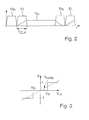
- the gain A comp is too Fig. 3 shown schematically.
- the comparator Comp has two thresholds different from 0.
- the loop gain A 0 (j ⁇ ) is dimensionless.
- the gain A comp has the unit 1 / volt. j is an imaginary number. ⁇ is the angular frequency.
- R 1 is the first resistance.
- C 1 is the first capacity.
- V ref is a reference voltage. As in Fig. 3 is shown, the gain A comp is the ratio of a dimensionless digital value to the input voltage of the comparator Comp.
- a ⁇ 0 2 ⁇ ⁇ ⁇ ⁇ f clk ⁇ f T .
- a ⁇ 0 2 ⁇ ⁇ ⁇ ⁇ f clk ⁇ f T .
- f T, A0 is the transit frequency of the loop gain A 0 (j ⁇ ).
- the phase rotation may amount to a maximum of 180 ° for sufficient stability.
- a constant ⁇ comp leads to a constant phase reserve and thus to a constant stability. The following applies to the relationship: f T .
- a ⁇ 0 f clk f T .
- a ⁇ 0 ⁇ ' constant
- the comparator Comp off Fig. 1 has a transfer function that is in Fig. 3 is shown schematically.
- the output signal is -1 for an input voltage less than -V th .
- the output signal is 0 for an input voltage between -V th and V th .
- the output signal is 1 for an input voltage greater than V th .
- the output signal of the comparator Comp is thus a ternary signal.
- comparators having more than three output states, such as five or seven output states, may be used.
- the linearized gain A comp of this three-state comparator Comp Fig. 1 is in Fig. 3 schematically and can be defined to: - > A comp ⁇ 1 / 2 ⁇ V th with the equation (7), the threshold voltage V th becomes: - > V th ⁇ V ref / R 1 ⁇ C 1 ⁇ f clk
- Fig. 1 is a possible implementation of a voltage source Cal for generating the threshold voltage V th shown schematically.
- the charge of a capacitor C 2 is periodically extinguished and recharged with a 1 / R 2 proportional current I ref for the duration T clk of a period of the clock frequency f clk .
- the resistor R 2 and a current mirror S with the mirror ratio of 1: 1 are connected to the voltage V ref .
- the control signal St I an associated switch is closed and the capacitor C 2 is charged with the current I ref for the duration T clk .
- the control signal ST R closes an associated switch and discharges the capacitance C 2 .
- Fig. 2 shows the diagram to voltage source Cal with the control signals St I , St R. Fig. 1 ,
- the dependence of loop stability on the parameters is eliminated by applying the proportionality relationship: R 1 ⁇ C 1 ⁇ R 2 ⁇ C 2
- the clock frequency can be changed, for example, by division or doubling to meet the condition according to equation (10).
- two different reference voltages eg V ref and V ref / 2.
- the resistors R 1 and R 2 are formed as a pairing structure.
- the capacitances C 1 and C 2 are formed as a pairing structure. It is also possible to use, as a resistor pairing structure, a matching structure with nested resistor elements for particularly high accuracy. It is also possible to use a matching structure with nested capacitance elements for particularly high accuracy as the capacity pairing structure.
- the time-continuous delta-sigma analog-to-digital converter of the embodiment of the Fig. 1 is advantageously integrated together with a sensor - in particular a Hall sensor - on a semiconductor chip.
- changes in the frequency f clk from 1/2 of the nominal value to 3 times the nominal value do not affect the transducer performance.
- the time-continuous delta-sigma analog-to-digital converter of the embodiment of the Fig. 1 is very robust against absolute value fluctuations.
- the invention is not limited to the illustrated embodiments of the FIGS. 1 to 3 limited.
- it is possible to specify another circuit for generating the threshold voltage V th which is a has corresponding dependence on T clk , R 2 , C 2 and V ref .
- the threshold voltages V th , 2V th and 3V th are generated, for example, by connecting several identical second capacitors in series, which are jointly charged by the current I ref and discharged at the same time. It is also possible to provide a higher-order time-continuous delta-sigma modulator, with all resistors and capacitors meeting the proportionality condition accordingly.
Landscapes
- Engineering & Computer Science (AREA)
- Theoretical Computer Science (AREA)
- Compression, Expansion, Code Conversion, And Decoders (AREA)
Abstract
Description
- Die vorliegende Erfindung betrifft einen zeitkontinuierlichen Delta-Sigma-Modulator.
- Aus "A 20mW 640-MHz CMOS Continuous-Time ΣΔ ADC With 20-MHz Signal Bandwidth, 80-dB Dynamic Range and 12bit ENOB", Mitteregger et al., IEEE JOURNAL OF SOLID_STATE CIRCUITS, VOL. 41, NO. 12, Dezember 2006, ist ein zeitkontinuierlicher Delta-Sigma-Analog-Digital-Umsetzer bekannt. Zur Eliminierung der Einflüsse auf die Schleifenstabilität werden die Schleifenkondensatoren getrimmt, entweder statisch oder auch im Betrieb. Dazu muss der passende diskrete Kondensatorwert ermittelt werden. Gegenüber einer statischen Trimmung kann nur eine dynamische Trimmung bei nicht-aktivem Modulator Temperatureinflüsse auf Widerstände und Taktfrequenz (fclk) eliminieren. Eine dynamische Trimmung bei aktivem Modulator kann kurzzeitig zu Wandlerfehlern führen.
- In der
DE 10 2008 020 452 A1 werden zusammengesetzte Halbleiterbauteile in einem Feld aus identischen (Halbleiter-)Elementen erzeugt, die auf einem Wafer um einen gemeinsamen Schwerpunkt herum verteilt angeordnet sind, um mögliche Gradienten von Inhomogenitäten von Prozessparametern (Schichtdicken, Dotierung etc.) auszugleichen, die sich durch Prozesstoleranzen entlang der Oberfläche ergeben. Die einzelnen Elemente werden relativ groß dimensioniert. - Der Erfindung liegt die Aufgabe zu Grunde, einen zeitkontinuierlichen Delta-Sigma-Modulator - insbesondere als Bestandteil eines Analog-Digital-Umsetzers - möglichst zu verbessern.
- Diese Aufgabe wird durch einen zeitkontinuierlichen Delta-Sigma-Modulator mit den Merkmalen des unabhängigen Anspruchs 1 gelöst. Vorteilhafte Weiterbildungen sind Gegenstand von abhängigen Ansprüchen und in der Beschreibung enthalten.
- Demzufolge ist ein zeitkontinuierlicher Delta-Sigma-Modulator vorgesehen.
- Der zeitkontinuierliche Delta-Sigma-Modulator weist einen Integrator und einen mit einer Taktfrequenz mittels Taktsignal getakteten Komparator auf. Der Integrator und der Komparator sind in einer Rückkopplungsschleife verbunden.
- Der zeitkontinuierliche Delta-Sigma-Modulator weist eine Spannungsquelle auf. Die Spannungsquelle ist mit dem Komparator zum Anlegen einer Schwellspannung an den Komparator verbunden.
- Eine Integrationszeitkonstante des Integrators weist einen ersten Widerstand und eine erste Kapazität auf.
- Die Spannungsquelle weist einen zweiten Widerstand und eine zweite Kapazität zur Einstellung der Schwellspannung auf.
- Der erste Widerstand und der zweite Widerstand sind Bestandteil einer Widerstandspaarungsstruktur.
- Die erste Kapazität und die zweite Kapazität sind Bestandteil einer Kapazitätspaarungsstruktur.
- Untersuchungen der Anmelderin haben gezeigt, dass die Widerstandspaarungsstruktur auf einem Halbleiterchip erzielt werden kann, indem der erste Widerstand und der zweite Widerstand durch die gleichen Prozessschritte hergestellt werden. Vorzugsweise sind der erste Widerstand und der zweite Widerstand auf dem Halbleiterchip elektrisch isoliert aneinander angrenzend angeordnet. Weiterhin kann die Kapazitätspaarungsstruktur auf dem Halbleiterchip erzielt werden, indem die erste Kapazität und die zweite Kapazität durch die gleichen Prozessschritte hergestellt werden. Vorzugsweise sind die erste Kapazität und der zweite Kapazität auf dem Halbleiterchip elektrisch isoliert aneinander angrenzend angeordnet. Durch eine konkrete Implementierung des Gegenstands des Anspruchs 1, wie diese beispielsweise im Ausführungsbeispiel der
Figur 1 erläutert ist, werden mehrere Vorteile erzielt. Die Stabilität der Schleifenverstärkung des zeitkontinuierlichen Delta-Sigma-Modulators wird für einen großen Bereich der Taktfrequenz erzielt. Weiterhin ist kein Messvorgang und damit verbundene Dimensionierung einer Regelung erforderlich. Die Schwellspannung wird durch die Spannungsquelle nicht geregelt, sondern gesteuert, was eine sehr schnelle Anpassung der Schwellspannung ermöglicht. Einflüsse von Temperaturänderungen und von fertigungsbedingten Abweichungen werden weitgehend reduziert. - Gemäß einer vorteilhaften Weiterbildung ist vorgesehen, dass der Komparator zur Änderung einer Schleifenverstärkung der Rückkopplungsschleife mittels der Schwellspannung ausgebildet ist.
- In einer vorteilhaften Weiterbildung ist die Spannungsquelle ausgebildet, die Schwellspannung aus den Eingangsgrößen einer Referenzspannung und einer Periode der Taktfrequenz und aus einer Zeitkonstante zu bilden. Die Zeitkonstante basiert auf dem zweiten Widerstand und der zweiten Kapazität.
- Gemäß einer vorteilhaften Weiterbildung weist die am Komparator anliegende Schwellspannung eine umgekehrt proportionale Abhängigkeit von dem Produkt aus dem ersten Widerstand und der ersten Kapazität und der Taktfrequenz auf.
- In einer vorteilhaften Weiterbildung weist die Spannungsquelle Halbleiterschalter zur Steuerung eines Entladens der zweiten Kapazität und zur Steuerung eines Ladens der zweiten Kapazität über den zweiten Widerstand für die Dauer einer Periode der Taktfrequenz auf.
- Die zuvor beschriebenen Weiterbildungsvarianten sind sowohl einzeln als auch in Kombination besonders vorteilhaft. Dabei können sämtliche Weiterbildungsvarianten untereinander kombiniert werden. Einige mögliche Kombinationen sind in der Beschreibung der Ausführungsbeispiele der Figuren erläutert. Diese dort dargestellten Möglichkeiten von Kombinationen der Weiterbildungsvarianten sind jedoch nicht abschließend.
- Im Folgenden wird die Erfindung durch Ausführungsbeispiele anhand zeichnerischer Darstellungen näher erläutert.
- Dabei zeigen
- Fig. 1
- einen schematischen Schaltplan eines zeitkontinuierlichen Delta-Sigma-Modulators,
- Fig. 2
- ein schematisches Diagramm von Steuersignalen, und
- Fig. 3
- ein schematisches Diagramm einer Übertragungsfunktion.
- In zeitkontinuierlichen Delta-Sigma-Modulatoren wird die Schleifenverstärkung durch die Integrationszeitkonstante RC beeinflusst. Die Qualität des so genannten Noise-Shapings und die Stabilität des Modulators hängen vom Verhältnis der Transitfrequenz der Schleifenverstärkung zur Taktfrequenz fclk ab. Durch Fertigungsschwankungen und Temperatureinflüsse können die Integrationszeitkonstante RC und die Taktfrequenz fclk schwanken.
- Ziel ist es daher zur kontinuierlichen Stabilisierung dieses Verhältnisses während des normalen Betriebs des Modulators Komparatorschwellen nachzuführen.
-
Fig. 1 zeigt ein vereinfachtes Modell eines zeitkontinuierlichen Delta-Sigma-Modulators erster Ordnung. Der zeitkontinuierliche Delta-Sigma-Modulator weist einen Integrator Int und einen Komparator Comp und einen Digital-Analog-Umsetzer DAC im Rückkopplungszweig auf. Eine Eingangsspannung Vin wird über einen Eingangswiderstand Rin in einen Eingangsstrom Iin gewandelt. Der Digital-Analog-Umsetzer DAC weist im Ausführungsbeispiel derFig. 1 ebenfalls einen Widerstand R1 auf, durch den der Ausgangsstrom IDAC des Digital-Analog-Umsetzers DAC fließt. Beide Ströme Iin und IDAC werden zum Summenstrom IS summiert und der Summenstrom IS durch den invertierenden Verstärker Inv mit Rückkopplung über eine erste Kapazität C1 in die Spannung Vint gewandelt. Der Integrator Int bewirkt daher eine Tiefpassfilterung. - Im Folgenden wird die Schleifenstabilität für den zeitkontinuierlichen Delta-Sigma-Modulator erster Ordnung der
Fig. 1 erläutert. Die Eingangsspannung Vin ist bei der Betrachtung der Schleifenstabilität bedeutungslos. Modulatorschleifen höherer Ordnung lassen sich für Frequenzen um die Transitfrequenz, die für die Stabilitätsbetrachtung entscheidend sind, näherungsweise durch eine Schleife erster Ordnung beschreiben. Aus diesem Grund gilt die nachfolgende Betrachtung auch für Schleifen höherer Ordnung entsprechend. - Gemäß dem Ausführungsbeispiel der
Fig. 1 ist eine Anwendung für Multibitsysteme vorgesehen. Im Ausführungsbeispiel derFig. 1 weist der Komparator Comp mehr als zwei Ausgangswerte auf, so dass sich dem Komparator Comp eine Verstärkung Acomp zuordnen lässt. Die Verstärkung Acomp ist zuFig. 3 schematisch dargestellt. Der Komparator Comp weist dabei zwei von 0 verschiedene Schwellen auf. - Die Schleifenverstärkung der Rückkoppelschleife in
Fig. 1 ist:
- Dabei ist die Schleifenverstärkung A0(jω) dimensionslos. Die Verstärkung Acomp besitzt die Einheit 1/Volt. j ist eine imaginäre Zahl. ω ist die Kreisfrequenz. R1 ist der erste Widerstand. C1 ist die erste Kapazität. Vref ist eine Referenzspannung. Wie in
Fig. 3 dargestellt ist, ist die Verstärkung Acomp das Verhältnis eines dimensionslosen Digitalwertes zur Eingangsspannung des Komparators Comp. - Die Verzögerung des Komparators ΔTcomp, die bei getakteten Systemen αTclk beträgt, führt zu einer zusätzlichen Phasendrehung in der Rückkoppelschleife gemäß

- Dabei ist fT,A0 die Transitfrequenz der Schleifenverstärkung A0(jω). Die Phasendrehung darf für hinreichende Stabilität maximal 180° betragen. Ein konstantes Δϕcomp führt zu konstanter Phasenreserve und somit zu gleichbleibender Stabilität. Dabei gilt für das Verhältnis:

- Die Transitfrequenz fT,A0 der Schleifenverstärkung lässt sich ermitteln zu:


- Die normierte Transitfrequenz FT,A0' ist dann:

- Somit gilt für die approximierte, linearisierte Verstärkung Acomp des Komparators Comp in
Fig. 1 :
- Der Komparator Comp aus
Fig. 1 weist eine Übertragungsfunktion auf, die inFig. 3 schematisch dargestellt ist. Das Ausgangssignal ist -1 für eine Eingangsspannung kleiner -Vth. Das Ausgangssignal ist 0 für eine Eingangsspannung zwischen -Vth und Vth. Das Ausgangssignal ist 1 für eine Eingangsspannung größer Vth. Das Ausgangssignal des Komparators Comp ist somit ein ternäres Signal. Alternativ zum Ausführungsbeispiel derFig. 1 können Komparatoren mit mehr als drei Ausgangszuständen, beispielsweise mit fünf oder sieben Ausgangszuständen verwendet werden. - Die linearisierte Verstärkung Acomp dieses Drei-Zustands-Komparators Comp aus
Fig. 1 ist inFig. 3 schematisch dargestellt und lässt sich definieren zu:
mit der Gleichung (7) wird die Schwellspannung Vth:
- Wenn also die Komparatorschwellen Vth eine umgekehrt proportionale Abhängigkeit von dem Produkt aus R1, C1 und fclk besitzen und proportional zur Referenzspannung Vref sind, dann wird die Abhängigkeit der Schleifenstabilität von diesen drei Parametern eliminiert.
- In
Fig. 1 ist eine mögliche Implementierung einer Spannungsquelle Cal zur Erzeugung der Schwellspannung Vth schematisch dargestellt. Dabei wird die Ladung einer Kapazität C2 periodisch gelöscht und mit einem 1/R2-proportionalen Strom Iref für die Dauer Tclk einer Periode der Taktfrequenz fclk wieder aufgeladen. Zur Erzeugung des Stroms Iref wird beispielsweise der Widerstand R2 und ein Stromspiegel S mit dem Spiegelverhältnis von 1 : 1 an die Spannung Vref angeschlossen. Durch das Steuersignal StI wird ein zugehöriger Schalter geschlossen und die Kapazität C2 mit dem Strom Iref für die Dauer Tclk geladen. Durch das Steuersignal STR wird ein zugehöriger Schalter geschlossen und die Kapazität C2 entladen. - Die Spannung Vth ergibt sich dann zu:

-
Fig. 2 zeigt das Diagramm zu Spannungsquelle Cal mit den Steuersignalen StI, StR ausFig. 1 . In diesem Ausführungsbeispiel wird die Abhängigkeit der Schleifenstabilität von den Parametern eliminiert, indem die Proportionalitätsbeziehung gilt:
- Im einfachsten Fall ist R1 = R2 = R und C1= C2 = C. Natürlich sind auch andere Verhältnisse möglich. Auch kann die Taktfrequenz z.B. durch Teilung oder Verdopplung geändert werden um die Bedingung gemäß Gleichung (10) zu erfüllen. Ebenfalls ist es möglich zwei unterschiedliche Referenzspannungen, z.B. Vref und Vref/2 zu verwenden. Die Widerstände R1 und R2 werden als Paarungsstruktur ausgebildet. Ebenfalls werden die Kapazitäten C1 und C2 als Paarungsstruktur ausgebildet. Ebenfalls ist es möglich, als Widerstandspaarungsstruktur eine Matchingstruktur mit ineinander verschachtelten Widerstandselementen für eine besonders hohe Genauigkeit zu verwenden. Ebenfalls ist es möglich, als Kapazitätspaarungsstruktur eine Matchingstruktur mit ineinander verschachtelten Kapazitätselementen für eine besonders hohe Genauigkeit zu verwenden.
- Der zeitkontinuierliche Delta-Sigma-Analog-Digital-Umsetzer des Ausführungsbeispiels der
Fig. 1 wird vorteilhafterweise zusammen mit einem Sensor - insbesondere einem Hallsensor - auf einem Halbleiterchip integriert. In einem von der Anmelderin entworfenen Schaltkreis beeinflussen Änderungen der Frequenz fclk von 1/2 des Nominalwertes bis zum 3-fache Nominalwert die Wandlerperformance nicht. Der zeitkontinuierliche Delta-Sigma-Analog-Digital-Umsetzer des Ausführungsbeispiels derFig. 1 ist sehr robust gegen Absolutwertschwankungen. - Die Erfindung ist nicht auf die dargestellten Ausgestaltungsvarianten der
Figuren 1 bis 3 beschränkt. Beispielsweise ist es möglich, eine andere Schaltung zur Erzeugung der Schwellspannung Vth anzugeben, die eine entsprechende Abhängigkeit von Tclk, R2, C2 und Vref hat. Wird ein Komparator mit beispielsweise drei positiven und drei negativen Schwellen verwendet, werden die Schwellspannungen Vth, 2Vth und 3Vth beispielsweise durch in Reihe schalten mehrerer identischer zweiter Kapazitäten erzeugt, die vom Strom Iref gemeinsam geladen und zeitgleich entladen werden. Auch ist es möglich, einen zeitkontinuierlichen Delta-Sigma-Modulator höherer Ordnung vorzusehen, wobei alle Widerstände und Kapazitäten die Proportionalitätsbedingung entsprechend erfüllen. -
- R1, R2, Rin
- Widerstand
- C1, C2
- Kapazität
- Inv
- invertierende Verstärker
- Int
- Integrator
- Comp
- Komparator
- DAC
- Digital-Analog-Umsetzer
- Cal
- Spannungsquelle
- S
- Stromspiegel
- fCLK
- Taktfrequenz
- TCLK
- Taktperiode
- AComp
- approximierte Verstärkung
- Vref
- Referenzspannung
- Vint
- Integratorausgangsspannung
- Iref
- Referenzstrom
- StI, StR
- Steuersignal
- Vth, -Vth
- Schwellspannung
- t
- Zeit
- B
- Komparatorausgangssignal
Claims (6)
- Zeitkontinuierlicher Delta-Sigma-Modulator,- mit einem Integrator (Int) und einem mit einer Taktfrequenz (fclk) getakteten Komparator (Comp), die in einer Rückkopplungsschleife verbunden sind,- mit einer Spannungsquelle (Cal), die mit dem Komparator (Comp) zum Anlegen einer Schwellspannung (Vth) an den Komparator (Comp) verbunden ist,- bei dem eine Integrationszeitkonstante des Integrators (Int) einen ersten Widerstand (R1) und eine erste Kapazität (C1) aufweist,- bei dem die Spannungsquelle (Cal) einen zweiten Widerstand (R2) und eine zweite Kapazität (C2) zur Einstellung der Schwellspannung (Vth) aufweist,- bei dem der erste Widerstand (R1) und der zweite Widerstand (R2) Bestandteil einer Widerstandspaarungsstruktur sind, und- bei dem die erste Kapazität (C1) und die zweite Kapazität (C2) Bestandteil einer Kapazitätspaarungsstruktur sind.
- Zeitkontinuierlicher Delta-Sigma-Modulator nach Anspruch 1,- bei dem der Komparator (Comp) zur Änderung einer Schleifenverstärkung (A0(jω)) der Rückkopplungsschleife mittels der Schwellspannung (Vth) ausgebildet ist.
- Zeitkontinuierlicher Delta-Sigma-Modulator nach einem der vorhergehenden Ansprüche,- bei dem die Spannungsquelle (Cal) ausgebildet ist, die Schwellspannung (Vth) aus den Eingangsgrößen einer Referenzspannung (Vref) und einer Periode (Tclk) der Taktfrequenz (fclk) und aus einer Zeitkonstante zu bilden, wobei die Zeitkonstante auf dem zweiten Widerstand (R2) und der zweiten Kapazität (C2) Kapazität (C2) basiert.
- Zeitkontinuierlicher Delta-Sigma-Modulator nach einem der vorhergehenden Ansprüche,- bei dem die Schwellspannung (Vth) eine umgekehrt proportionale Abhängigkeit von dem Produkt aus dem ersten Widerstand (R1) und der ersten Kapazität (C1) und der Taktfrequenz (fclk) aufweist.
- Zeitkontinuierlicher Delta-Sigma-Modulator nach einem der vorhergehenden Ansprüche,- bei dem die Spannungsquelle (Cal) Halbleiterschalter zur Steuerung eines Entladens der zweiten Kapazität (C2) und zur Steuerung eines Ladens der zweiten Kapazität (C2) über den zweiten Widerstand (R2) für die Dauer einer Periode (Tclk) der Taktfrequenz (fclk) aufweist.
- Zeitkontinuierlicher Delta-Sigma-Modulator nach einem der vorhergehenden Ansprüche,- bei dem die Rückkopplungsschleife weitere Integratoren zur Ausbildung des Delta-Sigma-Modulators einer Ordnung größer eins aufweist.
Applications Claiming Priority (1)
| Application Number | Priority Date | Filing Date | Title |
|---|---|---|---|
| DE102013007030.9A DE102013007030A1 (de) | 2013-04-24 | 2013-04-24 | Zeitkontinuierlicher Delta-Sigma-Modulator |
Publications (3)
| Publication Number | Publication Date |
|---|---|
| EP2797236A2 true EP2797236A2 (de) | 2014-10-29 |
| EP2797236A3 EP2797236A3 (de) | 2015-03-04 |
| EP2797236B1 EP2797236B1 (de) | 2018-08-22 |
Family
ID=50693415
Family Applications (1)
| Application Number | Title | Priority Date | Filing Date |
|---|---|---|---|
| EP14001368.1A Active EP2797236B1 (de) | 2013-04-24 | 2014-04-15 | Zeitkontinuierlicher Delta-Sigma-Modulator |
Country Status (4)
| Country | Link |
|---|---|
| US (1) | US9024795B2 (de) |
| EP (1) | EP2797236B1 (de) |
| JP (1) | JP5752293B2 (de) |
| DE (1) | DE102013007030A1 (de) |
Families Citing this family (10)
| Publication number | Priority date | Publication date | Assignee | Title |
|---|---|---|---|---|
| US10224951B2 (en) * | 2016-01-08 | 2019-03-05 | Analog Devices Global | Configurable input range for continuous-time sigma delta modulators |
| US10530372B1 (en) | 2016-03-25 | 2020-01-07 | MY Tech, LLC | Systems and methods for digital synthesis of output signals using resonators |
| US10020818B1 (en) | 2016-03-25 | 2018-07-10 | MY Tech, LLC | Systems and methods for fast delta sigma modulation using parallel path feedback loops |
| EP3542461B1 (de) | 2016-11-21 | 2024-07-31 | Mixed-Signal Devices Inc. | Hocheffiziente leistungsverstärkerarchitekturen für hf-anwendungen |
| CN109995367B (zh) | 2017-12-29 | 2022-12-06 | 瑞昱半导体股份有限公司 | 数模转换器装置 |
| TWI645684B (zh) * | 2017-12-29 | 2018-12-21 | 瑞昱半導體股份有限公司 | 三角積分調變器 |
| CN121000228A (zh) | 2019-03-14 | 2025-11-21 | 混合信号设备股份有限公司 | 数模转换器(dac)和模数转换器(adc)的线性化和相关方法 |
| WO2022170351A1 (en) | 2021-02-05 | 2022-08-11 | Mixed-Signal Devices Inc. | Systems and methods for digital signal chirp generation using frequency multipliers |
| US12231145B1 (en) | 2022-02-24 | 2025-02-18 | Mixed-Signal Devices Inc. | Systems and methods for digital signal synthesis with variable sample rate DAC |
| US11933919B2 (en) | 2022-02-24 | 2024-03-19 | Mixed-Signal Devices Inc. | Systems and methods for synthesis of modulated RF signals |
Citations (1)
| Publication number | Priority date | Publication date | Assignee | Title |
|---|---|---|---|---|
| DE102008020452A1 (de) | 2007-04-26 | 2008-11-06 | Atmel Germany Gmbh | Verfahren zur Erzeugung eines Layouts, Verwendung eines Transistorlayouts und Halbleiterschaltung |
Family Cites Families (11)
| Publication number | Priority date | Publication date | Assignee | Title |
|---|---|---|---|---|
| JPS63267017A (ja) * | 1987-04-24 | 1988-11-04 | Nec Corp | アナログ・デイジタル変換回路装置 |
| JPH0575468A (ja) * | 1991-09-12 | 1993-03-26 | Yokogawa Electric Corp | Σδ変調器 |
| DE50207726D1 (de) * | 2002-08-29 | 2006-09-14 | Infineon Technologies Ag | Quantisierer für einen Sigma-Delta-Modulator und Sigma-Delta-Modulator |
| US7095345B2 (en) * | 2004-06-29 | 2006-08-22 | Analog Devices, Inc. | Hybrid tuning circuit for continuous-time sigma-delta analog-to-digital converter |
| US7324028B2 (en) * | 2005-09-23 | 2008-01-29 | Realtek Semiconductor Corp. | Self-calibrating continuous-time delta-sigma modulator |
| WO2007085997A1 (en) * | 2006-01-25 | 2007-08-02 | Nxp B.V. | Continuous-time sigma-delta analog-to-digital converter with capacitor and/or resistance digital self-calibration means for rc spread compensation |
| US7948412B2 (en) * | 2006-08-23 | 2011-05-24 | Asahi Kasei Emd Corporation | Delta-sigma modulator |
| US7397291B1 (en) * | 2007-01-10 | 2008-07-08 | Freescale Semiconductor, Inc. | Clock jitter minimization in a continuous time sigma delta analog-to-digital converter |
| JP2010263483A (ja) * | 2009-05-08 | 2010-11-18 | Sony Corp | Δς変調器 |
| US8643518B2 (en) * | 2010-12-30 | 2014-02-04 | Mediatek Singapore Pte. Ltd. | Calibration of time constants in a continuous-time delta-sigma converter |
| KR20140001565A (ko) * | 2012-06-27 | 2014-01-07 | 한국전자통신연구원 | 시정수 보정 장치 및 방법과 이를 포함한 저역 통과 델타 시그마 변조 장치 |
-
2013
- 2013-04-24 DE DE102013007030.9A patent/DE102013007030A1/de not_active Withdrawn
-
2014
- 2014-04-15 EP EP14001368.1A patent/EP2797236B1/de active Active
- 2014-04-23 JP JP2014089397A patent/JP5752293B2/ja active Active
- 2014-04-24 US US14/260,899 patent/US9024795B2/en active Active
Patent Citations (1)
| Publication number | Priority date | Publication date | Assignee | Title |
|---|---|---|---|---|
| DE102008020452A1 (de) | 2007-04-26 | 2008-11-06 | Atmel Germany Gmbh | Verfahren zur Erzeugung eines Layouts, Verwendung eines Transistorlayouts und Halbleiterschaltung |
Non-Patent Citations (1)
| Title |
|---|
| MITTEREGGER ET AL.: "A 20mW 640-MHz CMOS Continuous-Time ?? ADC With 20-MHz Signal Bandwidth, 80-dB Dynamic Range and 12bit ENOB", IEEE JOURNAL OF SOLID_STATE CIRCUITS, vol. 41, no. 12, December 2006 (2006-12-01), XP011150731, DOI: doi:10.1109/JSSC.2006.884332 |
Also Published As
| Publication number | Publication date |
|---|---|
| EP2797236B1 (de) | 2018-08-22 |
| DE102013007030A1 (de) | 2014-10-30 |
| EP2797236A3 (de) | 2015-03-04 |
| JP2014217065A (ja) | 2014-11-17 |
| US20140320325A1 (en) | 2014-10-30 |
| US9024795B2 (en) | 2015-05-05 |
| JP5752293B2 (ja) | 2015-07-22 |
Similar Documents
| Publication | Publication Date | Title |
|---|---|---|
| EP2797236B1 (de) | Zeitkontinuierlicher Delta-Sigma-Modulator | |
| DE4200738C2 (de) | Digital/Analog-Wandler mit Filter hoher Ordnung | |
| DE69928057T2 (de) | Komparator and DA-Umsetzer mit geschalteten Kapazitäten | |
| DE19732840C2 (de) | Pipeline-Analog-Digital-Wandler | |
| DE69133008T2 (de) | Analog-Digital-Wandler und Vergleichschaltung dafür | |
| DE60111672T2 (de) | Delta-Sigma Analog-Digital-Wandler | |
| DE60128161T2 (de) | Verfahren und gerät zur anwendung in systemen mit geschalteten kapazitäten | |
| DE4200745C2 (de) | Verzerrungsarme Pufferschaltung mit Verstärkungsfaktor 1 für einen Digital/Analog-Wandler | |
| DE102007054519A1 (de) | Elektronische Schaltung und zeitlich fortlaufend arbeitender Delta-Sigma-Modulator | |
| DE102019219882B4 (de) | Strom-digital-präzisionswandler | |
| DE4200729C2 (de) | Verzerrungsarme Ausgangsstufe für einen Digital/Analog-Wandler | |
| DE10247133B4 (de) | Gesteuerte Stromquelle, insbesondere für Digital-Analog-Umsetzer in zeitkontinuierlichen Sigma-Delta-Modulatoren | |
| DE102017110976B3 (de) | Selbstoszillierender Mehrrampen-Umsetzer und Verfahren zum Umsetzen einer Kapazität in ein digitales Signal | |
| DE102021132279A1 (de) | Schaltung einschliesslich eines strom-digital-analogwandlers, verfahren zum betreiben eines strom-digital-analog-wandlers und zeitkontinuierlicher delta-sigma-wandler | |
| DE10341063B4 (de) | Vorwärtsverstärkende Filterschaltung | |
| DE102014114540A1 (de) | Verfahren und einrichtung zum verringern von kondensatorinduzierter isi in dacs | |
| DE60129356T2 (de) | Verfahren und gerät zur anwendung in systemen mit geschalteten kapazitäten | |
| DE10327621B4 (de) | Schaltungsanordnung und Verfahren zur Reduzierung eines Anpassungsfehlers in einem Sigma-Delta-Modulator | |
| DE102018109556B4 (de) | Verfahren, Vorrichtung und System zur Analog-Digital-Wandlung | |
| DE102014014257A1 (de) | Mehrstufige Quantisierer und Analog-Digital-Umsetzer | |
| DE102016112516B3 (de) | Signalumsetzer | |
| DE102010013812B4 (de) | Schaltungsanordnung und Verfahren zur kapazitiven Füllstandsmessung | |
| DE60216410T2 (de) | Mittelwertbildende Verstärkermatrix | |
| DE102018104530B4 (de) | Sigma-Delta-Wandler und entsprechende Verfahren | |
| DE102023116429B4 (de) | Zeitkontinuierlicher Sigma-Delta-Analog/Digital-Wandler |
Legal Events
| Date | Code | Title | Description |
|---|---|---|---|
| PUAI | Public reference made under article 153(3) epc to a published international application that has entered the european phase |
Free format text: ORIGINAL CODE: 0009012 |
|
| 17P | Request for examination filed |
Effective date: 20140415 |
|
| AK | Designated contracting states |
Kind code of ref document: A2 Designated state(s): AL AT BE BG CH CY CZ DE DK EE ES FI FR GB GR HR HU IE IS IT LI LT LU LV MC MK MT NL NO PL PT RO RS SE SI SK SM TR |
|
| AX | Request for extension of the european patent |
Extension state: BA ME |
|
| REG | Reference to a national code |
Ref country code: DE Ref legal event code: R079 Ref document number: 502014009238 Country of ref document: DE Free format text: PREVIOUS MAIN CLASS: H03M0003000000 Ipc: H03M0003020000 |
|
| PUAL | Search report despatched |
Free format text: ORIGINAL CODE: 0009013 |
|
| AK | Designated contracting states |
Kind code of ref document: A3 Designated state(s): AL AT BE BG CH CY CZ DE DK EE ES FI FR GB GR HR HU IE IS IT LI LT LU LV MC MK MT NL NO PL PT RO RS SE SI SK SM TR |
|
| AX | Request for extension of the european patent |
Extension state: BA ME |
|
| RIC1 | Information provided on ipc code assigned before grant |
Ipc: H03M 3/02 20060101AFI20150126BHEP Ipc: H03M 3/04 20060101ALI20150126BHEP |
|
| R17P | Request for examination filed (corrected) |
Effective date: 20150326 |
|
| RBV | Designated contracting states (corrected) |
Designated state(s): AL AT BE BG CH CY CZ DE DK EE ES FI FR GB GR HR HU IE IS IT LI LT LU LV MC MK MT NL NO PL PT RO RS SE SI SK SM TR |
|
| RAP1 | Party data changed (applicant data changed or rights of an application transferred) |
Owner name: TDK-MICRONAS GMBH |
|
| GRAP | Despatch of communication of intention to grant a patent |
Free format text: ORIGINAL CODE: EPIDOSNIGR1 |
|
| STAA | Information on the status of an ep patent application or granted ep patent |
Free format text: STATUS: GRANT OF PATENT IS INTENDED |
|
| INTG | Intention to grant announced |
Effective date: 20180507 |
|
| GRAS | Grant fee paid |
Free format text: ORIGINAL CODE: EPIDOSNIGR3 |
|
| GRAA | (expected) grant |
Free format text: ORIGINAL CODE: 0009210 |
|
| STAA | Information on the status of an ep patent application or granted ep patent |
Free format text: STATUS: THE PATENT HAS BEEN GRANTED |
|
| AK | Designated contracting states |
Kind code of ref document: B1 Designated state(s): AL AT BE BG CH CY CZ DE DK EE ES FI FR GB GR HR HU IE IS IT LI LT LU LV MC MK MT NL NO PL PT RO RS SE SI SK SM TR |
|
| REG | Reference to a national code |
Ref country code: GB Ref legal event code: FG4D Free format text: NOT ENGLISH |
|
| REG | Reference to a national code |
Ref country code: CH Ref legal event code: EP |
|
| REG | Reference to a national code |
Ref country code: AT Ref legal event code: REF Ref document number: 1033656 Country of ref document: AT Kind code of ref document: T Effective date: 20180915 |
|
| REG | Reference to a national code |
Ref country code: IE Ref legal event code: FG4D Free format text: LANGUAGE OF EP DOCUMENT: GERMAN |
|
| REG | Reference to a national code |
Ref country code: DE Ref legal event code: R096 Ref document number: 502014009238 Country of ref document: DE |
|
| REG | Reference to a national code |
Ref country code: NL Ref legal event code: MP Effective date: 20180822 |
|
| REG | Reference to a national code |
Ref country code: LT Ref legal event code: MG4D |
|
| PG25 | Lapsed in a contracting state [announced via postgrant information from national office to epo] |
Ref country code: SE Free format text: LAPSE BECAUSE OF FAILURE TO SUBMIT A TRANSLATION OF THE DESCRIPTION OR TO PAY THE FEE WITHIN THE PRESCRIBED TIME-LIMIT Effective date: 20180822 Ref country code: NL Free format text: LAPSE BECAUSE OF FAILURE TO SUBMIT A TRANSLATION OF THE DESCRIPTION OR TO PAY THE FEE WITHIN THE PRESCRIBED TIME-LIMIT Effective date: 20180822 Ref country code: NO Free format text: LAPSE BECAUSE OF FAILURE TO SUBMIT A TRANSLATION OF THE DESCRIPTION OR TO PAY THE FEE WITHIN THE PRESCRIBED TIME-LIMIT Effective date: 20181122 Ref country code: IS Free format text: LAPSE BECAUSE OF FAILURE TO SUBMIT A TRANSLATION OF THE DESCRIPTION OR TO PAY THE FEE WITHIN THE PRESCRIBED TIME-LIMIT Effective date: 20181222 Ref country code: BG Free format text: LAPSE BECAUSE OF FAILURE TO SUBMIT A TRANSLATION OF THE DESCRIPTION OR TO PAY THE FEE WITHIN THE PRESCRIBED TIME-LIMIT Effective date: 20181122 Ref country code: FI Free format text: LAPSE BECAUSE OF FAILURE TO SUBMIT A TRANSLATION OF THE DESCRIPTION OR TO PAY THE FEE WITHIN THE PRESCRIBED TIME-LIMIT Effective date: 20180822 Ref country code: RS Free format text: LAPSE BECAUSE OF FAILURE TO SUBMIT A TRANSLATION OF THE DESCRIPTION OR TO PAY THE FEE WITHIN THE PRESCRIBED TIME-LIMIT Effective date: 20180822 Ref country code: GR Free format text: LAPSE BECAUSE OF FAILURE TO SUBMIT A TRANSLATION OF THE DESCRIPTION OR TO PAY THE FEE WITHIN THE PRESCRIBED TIME-LIMIT Effective date: 20181123 Ref country code: LT Free format text: LAPSE BECAUSE OF FAILURE TO SUBMIT A TRANSLATION OF THE DESCRIPTION OR TO PAY THE FEE WITHIN THE PRESCRIBED TIME-LIMIT Effective date: 20180822 |
|
| PG25 | Lapsed in a contracting state [announced via postgrant information from national office to epo] |
Ref country code: HR Free format text: LAPSE BECAUSE OF FAILURE TO SUBMIT A TRANSLATION OF THE DESCRIPTION OR TO PAY THE FEE WITHIN THE PRESCRIBED TIME-LIMIT Effective date: 20180822 Ref country code: AL Free format text: LAPSE BECAUSE OF FAILURE TO SUBMIT A TRANSLATION OF THE DESCRIPTION OR TO PAY THE FEE WITHIN THE PRESCRIBED TIME-LIMIT Effective date: 20180822 Ref country code: LV Free format text: LAPSE BECAUSE OF FAILURE TO SUBMIT A TRANSLATION OF THE DESCRIPTION OR TO PAY THE FEE WITHIN THE PRESCRIBED TIME-LIMIT Effective date: 20180822 |
|
| PG25 | Lapsed in a contracting state [announced via postgrant information from national office to epo] |
Ref country code: RO Free format text: LAPSE BECAUSE OF FAILURE TO SUBMIT A TRANSLATION OF THE DESCRIPTION OR TO PAY THE FEE WITHIN THE PRESCRIBED TIME-LIMIT Effective date: 20180822 Ref country code: PL Free format text: LAPSE BECAUSE OF FAILURE TO SUBMIT A TRANSLATION OF THE DESCRIPTION OR TO PAY THE FEE WITHIN THE PRESCRIBED TIME-LIMIT Effective date: 20180822 Ref country code: CZ Free format text: LAPSE BECAUSE OF FAILURE TO SUBMIT A TRANSLATION OF THE DESCRIPTION OR TO PAY THE FEE WITHIN THE PRESCRIBED TIME-LIMIT Effective date: 20180822 Ref country code: ES Free format text: LAPSE BECAUSE OF FAILURE TO SUBMIT A TRANSLATION OF THE DESCRIPTION OR TO PAY THE FEE WITHIN THE PRESCRIBED TIME-LIMIT Effective date: 20180822 Ref country code: EE Free format text: LAPSE BECAUSE OF FAILURE TO SUBMIT A TRANSLATION OF THE DESCRIPTION OR TO PAY THE FEE WITHIN THE PRESCRIBED TIME-LIMIT Effective date: 20180822 Ref country code: IT Free format text: LAPSE BECAUSE OF FAILURE TO SUBMIT A TRANSLATION OF THE DESCRIPTION OR TO PAY THE FEE WITHIN THE PRESCRIBED TIME-LIMIT Effective date: 20180822 |
|
| REG | Reference to a national code |
Ref country code: DE Ref legal event code: R097 Ref document number: 502014009238 Country of ref document: DE |
|
| PG25 | Lapsed in a contracting state [announced via postgrant information from national office to epo] |
Ref country code: SK Free format text: LAPSE BECAUSE OF FAILURE TO SUBMIT A TRANSLATION OF THE DESCRIPTION OR TO PAY THE FEE WITHIN THE PRESCRIBED TIME-LIMIT Effective date: 20180822 Ref country code: SM Free format text: LAPSE BECAUSE OF FAILURE TO SUBMIT A TRANSLATION OF THE DESCRIPTION OR TO PAY THE FEE WITHIN THE PRESCRIBED TIME-LIMIT Effective date: 20180822 Ref country code: DK Free format text: LAPSE BECAUSE OF FAILURE TO SUBMIT A TRANSLATION OF THE DESCRIPTION OR TO PAY THE FEE WITHIN THE PRESCRIBED TIME-LIMIT Effective date: 20180822 |
|
| PLBE | No opposition filed within time limit |
Free format text: ORIGINAL CODE: 0009261 |
|
| STAA | Information on the status of an ep patent application or granted ep patent |
Free format text: STATUS: NO OPPOSITION FILED WITHIN TIME LIMIT |
|
| 26N | No opposition filed |
Effective date: 20190523 |
|
| PG25 | Lapsed in a contracting state [announced via postgrant information from national office to epo] |
Ref country code: SI Free format text: LAPSE BECAUSE OF FAILURE TO SUBMIT A TRANSLATION OF THE DESCRIPTION OR TO PAY THE FEE WITHIN THE PRESCRIBED TIME-LIMIT Effective date: 20180822 |
|
| REG | Reference to a national code |
Ref country code: CH Ref legal event code: PL |
|
| REG | Reference to a national code |
Ref country code: BE Ref legal event code: MM Effective date: 20190430 |
|
| PG25 | Lapsed in a contracting state [announced via postgrant information from national office to epo] |
Ref country code: LU Free format text: LAPSE BECAUSE OF NON-PAYMENT OF DUE FEES Effective date: 20190415 Ref country code: MC Free format text: LAPSE BECAUSE OF FAILURE TO SUBMIT A TRANSLATION OF THE DESCRIPTION OR TO PAY THE FEE WITHIN THE PRESCRIBED TIME-LIMIT Effective date: 20180822 |
|
| PG25 | Lapsed in a contracting state [announced via postgrant information from national office to epo] |
Ref country code: LI Free format text: LAPSE BECAUSE OF NON-PAYMENT OF DUE FEES Effective date: 20190430 Ref country code: CH Free format text: LAPSE BECAUSE OF NON-PAYMENT OF DUE FEES Effective date: 20190430 |
|
| PG25 | Lapsed in a contracting state [announced via postgrant information from national office to epo] |
Ref country code: BE Free format text: LAPSE BECAUSE OF NON-PAYMENT OF DUE FEES Effective date: 20190430 |
|
| PG25 | Lapsed in a contracting state [announced via postgrant information from national office to epo] |
Ref country code: TR Free format text: LAPSE BECAUSE OF FAILURE TO SUBMIT A TRANSLATION OF THE DESCRIPTION OR TO PAY THE FEE WITHIN THE PRESCRIBED TIME-LIMIT Effective date: 20180822 |
|
| PG25 | Lapsed in a contracting state [announced via postgrant information from national office to epo] |
Ref country code: IE Free format text: LAPSE BECAUSE OF NON-PAYMENT OF DUE FEES Effective date: 20190415 |
|
| PG25 | Lapsed in a contracting state [announced via postgrant information from national office to epo] |
Ref country code: PT Free format text: LAPSE BECAUSE OF FAILURE TO SUBMIT A TRANSLATION OF THE DESCRIPTION OR TO PAY THE FEE WITHIN THE PRESCRIBED TIME-LIMIT Effective date: 20181222 |
|
| PGFP | Annual fee paid to national office [announced via postgrant information from national office to epo] |
Ref country code: FR Payment date: 20200420 Year of fee payment: 7 |
|
| REG | Reference to a national code |
Ref country code: AT Ref legal event code: MM01 Ref document number: 1033656 Country of ref document: AT Kind code of ref document: T Effective date: 20190415 |
|
| PGFP | Annual fee paid to national office [announced via postgrant information from national office to epo] |
Ref country code: GB Payment date: 20200427 Year of fee payment: 7 |
|
| PG25 | Lapsed in a contracting state [announced via postgrant information from national office to epo] |
Ref country code: AT Free format text: LAPSE BECAUSE OF NON-PAYMENT OF DUE FEES Effective date: 20190415 |
|
| PG25 | Lapsed in a contracting state [announced via postgrant information from national office to epo] |
Ref country code: CY Free format text: LAPSE BECAUSE OF FAILURE TO SUBMIT A TRANSLATION OF THE DESCRIPTION OR TO PAY THE FEE WITHIN THE PRESCRIBED TIME-LIMIT Effective date: 20180822 |
|
| PG25 | Lapsed in a contracting state [announced via postgrant information from national office to epo] |
Ref country code: MT Free format text: LAPSE BECAUSE OF FAILURE TO SUBMIT A TRANSLATION OF THE DESCRIPTION OR TO PAY THE FEE WITHIN THE PRESCRIBED TIME-LIMIT Effective date: 20180822 Ref country code: HU Free format text: LAPSE BECAUSE OF FAILURE TO SUBMIT A TRANSLATION OF THE DESCRIPTION OR TO PAY THE FEE WITHIN THE PRESCRIBED TIME-LIMIT; INVALID AB INITIO Effective date: 20140415 |
|
| GBPC | Gb: european patent ceased through non-payment of renewal fee |
Effective date: 20210415 |
|
| PG25 | Lapsed in a contracting state [announced via postgrant information from national office to epo] |
Ref country code: GB Free format text: LAPSE BECAUSE OF NON-PAYMENT OF DUE FEES Effective date: 20210415 Ref country code: FR Free format text: LAPSE BECAUSE OF NON-PAYMENT OF DUE FEES Effective date: 20210430 |
|
| PG25 | Lapsed in a contracting state [announced via postgrant information from national office to epo] |
Ref country code: MK Free format text: LAPSE BECAUSE OF FAILURE TO SUBMIT A TRANSLATION OF THE DESCRIPTION OR TO PAY THE FEE WITHIN THE PRESCRIBED TIME-LIMIT Effective date: 20180822 |
|
| PGFP | Annual fee paid to national office [announced via postgrant information from national office to epo] |
Ref country code: DE Payment date: 20250422 Year of fee payment: 12 |