EP2775311A2 - Stromsensor - Google Patents
Stromsensor Download PDFInfo
- Publication number
- EP2775311A2 EP2775311A2 EP14155571.4A EP14155571A EP2775311A2 EP 2775311 A2 EP2775311 A2 EP 2775311A2 EP 14155571 A EP14155571 A EP 14155571A EP 2775311 A2 EP2775311 A2 EP 2775311A2
- Authority
- EP
- European Patent Office
- Prior art keywords
- current
- semiconductor chip
- conductor
- electrical connections
- magnetic field
- Prior art date
- Legal status (The legal status is an assumption and is not a legal conclusion. Google has not performed a legal analysis and makes no representation as to the accuracy of the status listed.)
- Granted
Links
Images


Classifications
-
- G—PHYSICS
- G01—MEASURING; TESTING
- G01R—MEASURING ELECTRIC VARIABLES; MEASURING MAGNETIC VARIABLES
- G01R1/00—Details of instruments or arrangements of the types included in groups G01R5/00 - G01R13/00 and G01R31/00
- G01R1/02—General constructional details
- G01R1/04—Housings; Supporting members; Arrangements of terminals
- G01R1/0408—Test fixtures or contact fields; Connectors or connecting adaptors; Test clips; Test sockets
- G01R1/0416—Connectors, terminals
-
- G—PHYSICS
- G01—MEASURING; TESTING
- G01R—MEASURING ELECTRIC VARIABLES; MEASURING MAGNETIC VARIABLES
- G01R15/00—Details of measuring arrangements of the types provided for in groups G01R17/00 - G01R29/00, G01R33/00 - G01R33/26 or G01R35/00
- G01R15/14—Adaptations providing voltage or current isolation, e.g. for high-voltage or high-current networks
- G01R15/20—Adaptations providing voltage or current isolation, e.g. for high-voltage or high-current networks using galvano-magnetic devices, e.g. Hall-effect devices, i.e. measuring a magnetic field via the interaction between a current and a magnetic field, e.g. magneto resistive or Hall effect devices
-
- G—PHYSICS
- G01—MEASURING; TESTING
- G01R—MEASURING ELECTRIC VARIABLES; MEASURING MAGNETIC VARIABLES
- G01R15/00—Details of measuring arrangements of the types provided for in groups G01R17/00 - G01R29/00, G01R33/00 - G01R33/26 or G01R35/00
- G01R15/14—Adaptations providing voltage or current isolation, e.g. for high-voltage or high-current networks
- G01R15/20—Adaptations providing voltage or current isolation, e.g. for high-voltage or high-current networks using galvano-magnetic devices, e.g. Hall-effect devices, i.e. measuring a magnetic field via the interaction between a current and a magnetic field, e.g. magneto resistive or Hall effect devices
- G01R15/202—Adaptations providing voltage or current isolation, e.g. for high-voltage or high-current networks using galvano-magnetic devices, e.g. Hall-effect devices, i.e. measuring a magnetic field via the interaction between a current and a magnetic field, e.g. magneto resistive or Hall effect devices using Hall-effect devices
-
- G—PHYSICS
- G01—MEASURING; TESTING
- G01R—MEASURING ELECTRIC VARIABLES; MEASURING MAGNETIC VARIABLES
- G01R15/00—Details of measuring arrangements of the types provided for in groups G01R17/00 - G01R29/00, G01R33/00 - G01R33/26 or G01R35/00
- G01R15/14—Adaptations providing voltage or current isolation, e.g. for high-voltage or high-current networks
- G01R15/20—Adaptations providing voltage or current isolation, e.g. for high-voltage or high-current networks using galvano-magnetic devices, e.g. Hall-effect devices, i.e. measuring a magnetic field via the interaction between a current and a magnetic field, e.g. magneto resistive or Hall effect devices
- G01R15/207—Constructional details independent of the type of device used
Definitions
- IC Integrated Circuit
- Current sensors are available in many versions and variants.
- Current sensors which detect the magnetic field generated by the current are packaged in a conventional IC package and in which the current conductor through which the current to be measured flows through the housing are known, for example EP 1443332 .
- WO 2006130393 and DE 102009054892 Such current sensors include a current conductor formed as a part of the leadframe used for the assembly and manufacture of the electrical leads, and a semiconductor chip mounted on the leadframe, the at least one magnetic field sensor, and for its operation and processing of its output signal having necessary electronics.
- the current conductor passed through the housing has a relatively small cross section and has a further reduced cross section in the region of the magnetic field sensors in order to locally increase the current density and hence the magnetic field, the heat resulting from the power loss in the conductor leads to a heating of the current sensor. causes the unwanted drift fluctuations of the magnetic field sensors.
- the current conductor and the electronics integrated in the semiconductor chip must be electrically insulated from one another, wherein the insulation is required to have a predetermined dielectric strength, which is typically 2 to 4 kV.
- the invention has for its object to develop a current sensor for relatively high rated current and high voltage resistance, which takes up little space and is inexpensive to produce.
- a current sensor comprises a housing made of plastic, a current conductor with molded-on first and second electrical terminals, through which a current to be measured is supplied and removed, third electrical connections, and a semiconductor chip having an active surface with at least one magnetic field sensor which is sensitive on a component of the magnetic field which is perpendicular to the active surface of the semiconductor chip and which is generated by the current flowing through the current conductor, the first and second electrical connections on a first side of the housing and the third electrical connections on an opposite side of the first side Housing are arranged, wherein the active surface of the semiconductor chip facing the current conductor and electrical connection pads of the semiconductor chip via first bumps to the third electrical terminals are connected, and wherein the semiconductor chip has second bumps, di e are electrically isolated from the active surface of the semiconductor chip by an insulating layer and on rest on the conductor or on formed on the conductor extensions.
- the ends of the third electrical connections lying above the semiconductor chip are arranged substantially along a line, and an adjacent edge of the current conductor runs parallel to the line, so that all third electrical connections are approximately equidistant from the current conductor.
- the current conductor has at least two extensions which extend to the edge of the housing and are exposed there.
- the insulating layer preferably has a layer of organic material.
- the organic material may be polyimide.
- the surface of the bulk material of the semiconductor chip and the second bumps there are no electrically conductive structures made of a metallization layer present for the production of electrical connections.
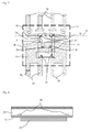
- the Fig. 1 shows in plan view of a current sensor according to the invention.
- the current sensor comprises a semiconductor chip 1 with at least one magnetic field sensor 2 and electronic circuits for the operation of the at least one magnetic field sensor 2 and the processing of the measurement signal supplied by the at least one magnetic field sensor 2.
- the current sensor further comprises a flat conductor 3, whose ends are designed as first electrical connections 4 and second electrical connections 5, and third electrical connections 6.
- the third electrical connections 6 serve to supply the electronic circuits with electrical energy and to output an output signal , Their number is at least three, in the example four.
- the conductor 3 and the semiconductor chip 1 are in one Packed IC housing 7, wherein the electrical connections 4, 5 and 6 either as IC legs protrude from the housing 7 (eg in a SOIC-8 or SOIC-16 housing) or on the bottom and / or side walls of the housing 7 exposed (eg in a QFN housing).
- the conductor 3 and the electrical connections 4, 5 and 6 are parts of a so-called lead frame, which was used for the production.
- the electrical connections 4 and 5 are arranged on a first side of the housing 7, the electrical connections 6 are arranged on a second, the first opposite side of the housing 7.
- the semiconductor chip 1 is mounted as a flip chip, ie its active surface, into which the at least one magnetic field sensor 2 and the electronic circuits are integrated, faces the current conductor 3 and so-called first "bumps" 8 provide the electrical connections between the semiconductor chip 1 and the electrical connections 6 ago.
- second bumps 9 are arranged between the current conductor 3 and the semiconductor chip 1, but do not produce an electrical connection between the semiconductor chip 1 and the current conductor 3, but are separated from the semiconductor chip 1 by an insulating layer, as described in detail in FIG Fig. 2 is shown.
- the insulating layer may consist of a single electrically non-conductive layer, for example a passivation layer, or of two or more superimposed, electrically non-conductive, ie electrically insulating, layers.
- the current conductor 3 is substantially U-shaped, the U being formed of three sections, namely a first section comprising the first electrical connections 4, a second elongated section with parallel edges 12 and a third section comprising the second electrical connections 5 includes.
- the current conductor 3 has two first electrical connections 4 and two second electrical connections 5 which protrude out of the housing 7 as connection legs.
- the protruding from the housing 7 ends of the terminal pins of the first electrical connections 4 may in turn be connected to each other, ie be designed as so-called fused leads, as well as protruding from the housing 7 ends of the terminal legs of the second electrical connections 5.
- Each magnetic field sensor 2 is preferably a Hall element or a cluster of Hall elements.
- the first bumps 8 and the second bumps 9 are applied to the semiconductor chip 1, wherein the first bumps 8 have electrical connection surfaces 13 (FIG. Fig. 2 ) of the semiconductor chip 1, while the second bumps 9 from the active surface of the semiconductor chip 1 through the insulating layer are galvanically isolated.
- the semiconductor chip 1 is placed as a flip chip on the leadframe.
- the first bumps 8 rest on the electrical connections 6 and establish the electrical connections between the semiconductor chip 1 and the electrical connections 6.
- the second bumps 9 are located on the conductor 3.
- Their task is to support the semiconductor chip 1, so that the active surface of the semiconductor chip 1 is aligned parallel to the surface of the conductor 3 and this remains during packaging in the housing 7, which takes place by casting in a mold.
- the insulation layer has the effect that the second bumps 9 and thus also the current conductor 3 are galvanically separated from the semiconductor chip 1.
- the current sensor according to the invention is designed to achieve, on the one hand, a high dielectric strength and, on the other hand, the highest possible rated current for a given standard IC package.
- the two goals are achieved in that the ends of the third electrical connections 6 situated below the flip chip are arranged essentially along a line 11 which runs parallel to the adjacent edge 12 of the middle section of the current conductor 3, so that all third electrical connections 6 are approximately at the same distance A away from the conductor 3.
- the distance A is dimensioned so large that the required dielectric strength is given.
- the arrangement of the third electrical connections 6 along the line 11 makes it possible for the conductor 3 to fill out the area available within the housing 7 to a large extent, namely except for recesses and / or holes in the conductor 3, which prevent delamination of conductor 3 and housing 7 are necessary.
- the current conductor 3 has a relatively large width everywhere, which reduces its electrical resistance to a minimum possible value and thus ensures on the one hand to minimize the power loss with given housing dimensions and on the other hand efficiently dissipate the resulting heat to the environment.
- the first bumps 8 and the second bumps 9 are at a distance B apart. They are preferably arranged in the vicinity of mutually opposite edges of the semiconductor chip 1, so that the distance B is maximum. The distance B can also be smaller.
- the support function of the second bumps 9 is usually fulfilled when B> A, since the distance A is typically at least one quarter to one third of the side length of the semiconductor chip 1.
- two second bumps 9 are present, but it can also be provided only a single second bump 9, which is then to be arranged approximately on the central axis of the semiconductor chip 1.
- the passivation layer 14 is electrically non-conductive.
- a further electrically non-conductive layer 15 is applied, whose thickness is dimensioned so large that the required between the conductor 3 and the semiconductor chip 1 dielectric strength is achieved.
- a material for the electrically non-conductive layer 15 is suitable in particular an organic material.
- An example of a preferred organic material is polyimide.
- the thickness of the electrically non-conductive layer 15 is typically in a range of 10-20 microns, but it can also reach higher values of 30 or even 40 microns.
- the passivation layer 14 and the electrically non-conductive layer 15 together form a two-layer insulation layer, which in Fig. 2 shown and designated there by the reference numeral 10.
- the current conductor 3 has an electrical resistance, which is why the current flowing through the current conductor 3 generates heat which has to be dissipated to the environment. In order to minimize the heat generated by the maximum allowable current, the conductor 3 is to be made as wide as possible along its entire length. On the other hand, the width of the current conductor 3 in the region of the at least one magnetic field sensor 2 should be made as narrow as possible in order to maximize the magnetic field generated by the current flowing through the current conductor 3.
- the thickness of the conductor 3 is uniform, because it is predetermined by the thickness of the leadframe.
- the geometry of the connection legs, ie here in particular their width W 1 is predetermined by standards.
- the width of the conductor 3 is advantageously wider everywhere than the predetermined width W 1 of the connection legs.
- the current conductor 3 can be formed with additional holes or slots, if necessary, to exclude delamination from the housing 7.
- extensions 16 are originally connected to the frame of the leadframe, but at the end of the production process, together with the electrical terminals 4, 5 and 6 are separated from the frame of the leadframe.
- the extensions 16 are therefore exposed at the edge of the housing 7.
- two extensions 16 are provided, which are arranged in the extension of the central portion of the conductor 3.
- the Fig. 2 shows in a non-scale representation in section the semiconductor chip 1 with a first bump 8 and a second bump 9.
- the bumps 8 and 9 are made in a standard technology, for example comprising a metal layer 17, a copper layer 18 and a solder layer 19.
- the bumps 8 and 9 can also be made of other materials.
- the metal layer 17 may also be a layer sequence of two or more materials, so that the metal layer 17 on the one hand adhere well and on the other hand can serve as a seed layer for the galvanic application of the copper layer 18.
- the bumps 8 and 9 are melted and soldered to the third electrical connections 6 or the current conductor 3.
- the first bumps 8 establish the electrical connections to the electrical connection surfaces 13 on the semiconductor chip 1, while in the case of the second bumps 9, the insulation layer 10 establishes an electrical connection between the current conductor 3 and the semiconductor chip 1 prevented.
- the surface of the bulk material of the semiconductor chip 1 and the second bumps 9 there are no electrically conductive structures made of a metallization layer, such as the metallization layer of the pad 13, for the production of the electrical connections in order to further increase the dielectric strength.
- the Fig. 3 shows a plan view of a second embodiment of a current sensor according to the invention, which is designed for a SOIC-16 housing.
- the current conductor 3 has two integrally formed extensions, above which the second bumps 9 are arranged. These extensions make it possible, on the one hand, to arrange the first bumps 8 and second bumps 9 each near an edge of the semiconductor chip 1 and, on the other hand, to arrange the semiconductor chip 1 approximately symmetrically with respect to the longitudinal axis of the current conductor 3 in its middle section.
- the current conductor 3 is a relatively large-area heat source with respect to the semiconductor chip 1, so that in the area of the magnetic field sensors 2 and the analog electronic circuits necessary for the operation of the magnetic field sensors 2 no temperature gradient arises.
- the Fig. 4 shows in plan view a third embodiment of a current sensor according to the invention, which is designed and optimized for a QFN housing
- the Fig. 5 shows the current sensor from below, ie its bottom.
- the leadframe includes first regions 20 of nominal thickness and second regions 21 of reduced thickness.
- the first regions 20 are exposed at the bottom of the housing 7, the second regions 21 are located inside the housing 7.
- the first regions 20 correspond to the terminals of the current sensor, via which the current sensor is connected to a printed circuit board.
- To increase the mechanical stability of the current conductor 3 is also formed in this embodiment advantageously with the extensions 16, which are originally connected to the frame of the leadframe, but at the end of the production process together with the electrical terminals 4, 5 and 6 from the frame of the leadframe be separated.
- the extensions 16 are exposed at the edge of the housing 7.
- two extensions 16 are provided in the extension of the central portion of the conductor 3 on both sides.
- the Fig. 6 shows a variant of the current sensor of the second embodiment, in which the central portion of the current conductor 3 in the region of the two magnetic field sensors 2 narrowed and the distance between the two magnetic field sensors is reduced 2.
- the Fig. 7 shows a further variant of the current sensor of the second embodiment, in which the middle portion of the current conductor 3 in the region of the two magnetic field sensors 2 by two slots 22 "S-shaped" is formed.
- the slots 22 are arranged so that the current conductor 3 is narrowed in the region of the two magnetic field sensors 2 and the magnetic field sensors 2 encloses a U-shape.
- current sensor increases the sensitivity at the expense of a lower rated current achieved.
- the Fig. 8 shows in cross section, but not to scale, an embodiment of a current sensor according to the invention, in which the current conductor 3 on three sides completely and on the semiconductor chip 1 opposite fourth side is covered only in edge regions with a ferromagnetic layer 23.
- the ferromagnetic layer 23 extends so far that it covers the magnetic field sensors 2.
- the thickness of the ferromagnetic layer 23 is about 50 to 100 ⁇ m, or more. It represents a magnetic yoke that amplifies the magnetic field generated by the current flowing through the current conductor 3 at the location of the magnetic field sensors 2.
- the ferromagnetic layer 23 is applied to the current conductor 3 by electroplating, for example.
- the Fig. 9 shows in cross section, but not to scale, an embodiment of a current sensor according to the invention, in which on the back of the semiconductor chip 1, a ferromagnetic layer 24 is applied.
- the ferromagnetic layer 24 lowers the magnetic resistance for the magnetic field generated by the current conductor 3 and amplifies this. In addition, it acts as a shield for external magnetic fields, which run parallel to the plane spanned by the semiconductor chip 1 level.
- Fig. 8 and Fig. 9 may also be combined so that both ferromagnetic layers 23 and 24 are present.
- the inventive design of the current sensors for example, meets the requirements of the standard UL 60950-1.
Landscapes
- Physics & Mathematics (AREA)
- General Physics & Mathematics (AREA)
- Measuring Instrument Details And Bridges, And Automatic Balancing Devices (AREA)
- Measuring Magnetic Variables (AREA)
- Wire Bonding (AREA)
- Hall/Mr Elements (AREA)
Abstract
Description
- Die Erfindung betrifft einen Stromsensor, insbesondere einen in einem IC Gehäuse (IC = Integrated Circuit) verpackten Stromsensor, bei dem der Stromleiter durch das Gehäuse führt.
- Stromsensoren gibt es in vielen Ausführungen und Varianten. Stromsensoren, die das vom Strom erzeugte Magnetfeld erfassen, in einem herkömmlichen IC Gehäuse verpackt sind und bei denen der Stromleiter, durch den der zu messende Strom fliesst, durch das Gehäuse geführt ist, sind beispielsweise bekannt aus
EP 1443332 ,WO 2005026749 ,WO 2006130393 undDE 102009054892 . Solche Stromsensoren enthalten einen Stromleiter, der als ein Teil des Leadframes ausgebildet ist, das für die Montage und die Herstellung der elektrischen Anschlüsse verwendet wird, und einen auf dem Leadframe montierten Halbleiterchip, der mindestens einen Magnetfeldsensor und die für dessen Betrieb und die Verarbeitung seines Ausgangssignals nötige Elektronik aufweist. - Weil der durch das Gehäuse geführte Stromleiter einen relativ kleinen Querschnitt hat und im Bereich der Magnetfeldsensoren einen nochmals reduzierten Querschnitt aufweist, um dort die Stromdichte und damit das Magnetfeld lokal zu erhöhen, führt die durch die Verlustleistung im Stromleiter entstehende Wärme zu einer Erwärmung des Stromsensors, die unerwünschte Driftschwankungen der Magnetfeldsensoren bewirkt. Der Stromleiter und die im Halbleiterchip integrierte Elektronik müssen elektrisch voneinander isoliert sein, wobei von der Isolation eine vorbestimmte Spannungsfestigkeit verlangt wird, die typischerweise 2 bis 4 kV beträgt.
- Der Erfindung liegt die Aufgabe zugrunde, einen Stromsensor für relativ hohen Nennstrom und hohe Spannungsfestigkeit zu entwickeln, der wenig Platz beansprucht und kostengünstig herstellbar ist.
- Die genannte Aufgabe wird erfindungsgemäss gelöst durch die Merkmale des Anspruchs 1. Vorteilhafte Ausgestaltungen ergeben sich aus den abhängigen Ansprüchen.
- Ein erfindungsgemässer Stromsensor umfasst ein Gehäuse aus Kunststoff, einen Stromleiter mit angeformten ersten und zweiten elektrischen Anschlüssen, durch die ein zu messender Strom zu- und abgeführt wird, dritte elektrische Anschlüsse, und einen Halbleiterchip mit einer aktiven Oberfläche mit wenigstens einem Magnetfeldsensor, der empfindlich ist auf eine senkrecht zur aktiven Oberfläche des Halbleiterchips verlaufende Komponente des Magnetfeldes, das von dem durch den Stromleiter fliessenden Strom erzeugt wird, wobei die ersten und zweiten elektrischen Anschlüsse an einer ersten Seite des Gehäuses und die dritten elektrischen Anschlüsse an einer der ersten Seite gegenüberliegenden Seite des Gehäuses angeordnet sind, wobei die aktive Oberfläche des Halbleiterchips dem Stromleiter zugewandt und elektrische Anschlussflächen des Halbleiterchips über erste Bumps mit den dritten elektrischen Anschlüssen verbunden sind, und wobei der Halbleiterchip zweite Bumps aufweist, die von der aktiven Oberfläche des Halbleiterchips durch eine Isolationsschicht galvanisch getrennt sind und auf dem Stromleiter oder auf an dem Stromleiter angeformten Fortsätzen aufliegen.
- Bevorzugt sind die über dem Halbleiterchip liegenden Enden der dritten elektrischen Anschlüsse im Wesentlichen entlang einer Linie angeordnet sind und eine benachbarte Kante des Stromleiters verläuft parallel zur Linie, so dass alle dritten elektrischen Anschlüsse annähernd im gleichen Abstand vom Stromleiter entfernt sind.
- Bevorzugt weist der Stromleiter wenigstens zwei Fortsätze auf, die sich bis an den Rand des Gehäuses erstrecken und dort freiliegen.
- Bevorzugt weist die Isolationsschicht eine Schicht aus organischem Material auf. Das organische Material kann Polyimid sein.
- Bevorzugt sind zwischen der Oberfläche des Bulk-Materials des Halbleiterchips und den zweiten Bumps keine elektrisch leitenden Strukturen aus einer für die Herstellung von elektrischen Verbindungen vorhandenen Metallisierungsschicht vorhanden.
- Die Erfindung wird nachfolgend anhand der Zeichnung näher erläutert.
- Fig. 1
- zeigt in Aufsicht ein erstes Ausführungsbeispiel eines erfindungsgemässen Stromsensors, und
- Fig. 2
- zeigt im Schnitt einen Halbleiterchip mit Bumps,
- Fig. 3
- zeigt in Aufsicht ein zweites Ausführungsbeispiel eines erfindungsgemässen Stromsensors,
- Fig. 4, 5
- zeigen in Aufsicht und von unten ein drittes Ausführungsbeispiel eines erfindungsgemässen Stromsensors,
- Fig. 6, 7
- zeigen in Aufsicht weitere Ausführungsbeispiele von erfindungsgemässen Stromsensoren, und
- Fig. 8, 9
- zeigen im Schnitt weitere Ausführungsbeispiele von erfindungsgemässen Stromsensoren.
- Die
Fig. 1 zeigt in Aufsicht einen erfindungsgemässen Stromsensor. Der Stromsensor umfasst einen Halbleiterchip 1 mit wenigstens einem Magnetfeldsensor 2 und elektronischen Schaltkreisen für den Betrieb des wenigstens einen Magnetfeldsensors 2 und die Verarbeitung des von dem mindestens einen Magnetfeldsensor 2 gelieferten Messsignals. Der Stromsensor umfasst weiter einen flachen Stromleiter 3, dessen Enden als erste elektrische Anschlüsse 4 und zweite elektrische Anschlüsse 5 ausgeführt sind, und dritte elektrische Anschlüsse 6. Die dritten elektrischen Anschlüsse 6 dienen zur Versorgung der elektronischen Schaltkreise mit elektrischer Energie und für die Ausgabe eines Ausgangssignals. Ihre Anzahl beträgt mindestens drei, im Beispiel vier. Der Stromleiter 3 und der Halbleiterchip 1 sind in ein IC Gehäuse 7 verpackt, wobei die elektrischen Anschlüsse 4, 5 und 6 entweder als IC Beinchen aus dem Gehäuse 7 herausragen (z.B. bei einem SOIC-8 oder SOIC-16 Gehäuse) oder an der Unterseite und/oder Seitenwänden des Gehäuses 7 freiliegen (z.B. bei einem QFN Gehäuse). Der Stromleiter 3 und die elektrischen Anschlüsse 4, 5 und 6 sind Teile eines so genannten Leadframes, das für die Herstellung verwendet wurde. Die elektrischen Anschlüsse 4 und 5 sind auf einer ersten Seite des Gehäuses 7, die elektrischen Anschlüsse 6 sind auf einer zweiten, der ersten gegenüberliegenden Seite des Gehäuses 7 angeordnet. Der Halbleiterchip 1 ist als Flipchip montiert, d.h. seine aktive Oberfläche, in die der mindestens eine Magnetfeldsensor 2 und die elektronischen Schaltkreise integriert sind, ist dem Stromleiter 3 zugewandt und so genannte erste "Bumps" 8 stellen die elektrischen Verbindungen zwischen dem Halbleiterchip 1 und den elektrischen Anschlüssen 6 her. Zwischen dem Stromleiter 3 und dem Halbleiterchip 1 sind zusätzlich zweite Bumps 9 angeordnet, die jedoch keine elektrische Verbindung zwischen dem Halbleiterchip 1 und dem Stromleiter 3 herstellen, sondern vom Halbleiterchip 1 durch eine Isolationsschicht getrennt sind, wie dies im Detail in derFig. 2 gezeigt ist. Die Isolationsschicht kann aus einer einzigen elektrisch nicht leitenden Schicht, z.B. einer Passivierungsschicht, oder aus zwei oder mehr übereinander liegenden, elektrisch nicht leitenden, d.h. elektrisch isolierenden, Schichten bestehen. - Der Stromleiter 3 ist im wesentlichen U-förmig, wobei das U aus drei Abschnitten gebildet ist, nämlich einem ersten Abschnitt, der die ersten elektrischen Anschlüsse 4 umfasst, einem zweiten länglichen Abschnitt mit parallelen Kanten 12 und einem dritten Abschnitt, der die zweiten elektrischen Anschlüsse 5 umfasst. Bei dem in der
Fig. 1 gezeigten Ausführungsbeispiel des erfindungsgemässen Stromsensors hat der Stromleiter 3 zwei erste elektrische Anschlüsse 4 und zwei zweite elektrische Anschlüsse 5, die als Anschlussbeinchen aus dem Gehäuse 7 herausragen. Die aus dem Gehäuse 7 herausragenden Enden der Anschlussbeinchen der ersten elektrischen Anschlüsse 4 können ihrerseits miteinander verbunden sein, d.h. als so genannte fused leads ausgeführt sein, ebenso die aus dem Gehäuse 7 herausragenden Enden der Anschlussbeinchen der zweiten elektrischen Anschlüsse 5. Bevorzugt sind zwei Magnetfeldsensoren 2 oder Cluster von Magnetfeldsensoren vorgesehen, die beidseitig des mittleren Abschnitts im Bereich der Kanten 12 des Stromleiters 3 angeordnet sind. Da das Magnetfeld, das von dem durch den Stromleiter 3 fliessenden Strom erzeugt wird, am Ort der beiden Magnetfeldsensoren 2 in entgegengesetzte Richtungen zeigt, werden die Ausgangssignale der beiden Magnetfeldsensoren 2 voneinander subtrahiert (Differenzschaltung). Auf diese Weise kann der Einfluss eines homogenen externen Störfeldes eliminiert werden. Jeder Magnetfeldsensor 2 ist bevorzugt ein Hallelement oder ein Cluster von Hallelementen. - Die ersten Bumps 8 und die zweiten Bumps 9 werden auf den Halbleiterchip 1 aufgebracht, wobei die ersten Bumps 8 elektrische Anschlussflächen 13 (
Fig. 2 ) des Halbleiterchips 1 kontaktieren, während die zweiten Bumps 9 von der aktiven Oberfläche des Halbleiterchips 1 durch die Isolationsschicht galvanisch getrennt sind. Bei der Herstellung des Stromsensors wird der Halbleiterchip 1 als Flipchip auf dem Leadframe platziert. Die ersten Bumps 8 liegen auf den elektrischen Anschlüssen 6 auf und stellen die elektrischen Verbindungen zwischen dem Halbleiterchip 1 und den elektrischen Anschlüssen 6 her. Die zweiten Bumps 9 liegen auf dem Stromleiter 3 auf. Ihre Aufgabe ist, den Halbleiterchip 1 zu stützen, damit die aktive Oberfläche des Halbleiterchips 1 parallel zur Oberfläche des Stromleiters 3 ausgerichtet ist und dies auch während des Verpackens im Gehäuse 7 bleibt, das durch Vergiessen in einer Form erfolgt. Die Isolationsschicht bewirkt, dass die zweiten Bumps 9 und somit auch der Stromleiter 3 galvanisch vom Halbleiterchip 1 getrennt sind. - Der erfindungsgemässe Stromsensor ist dahingehend ausgelegt, bei einem vorgegebenen Standard IC Gehäuse einerseits eine hohe Spannungsfestigkeit und andererseits einen möglichst hohen Nennstrom zu erreichen. Die beiden Ziele werden dadurch erreicht, dass die unter dem Flipchip liegenden Enden der dritten elektrischen Anschlüsse 6 im Wesentlichen entlang einer Linie 11 angeordnet sind, die parallel zu der benachbarten Kante 12 des mittleren Abschnitts des Stromleiters 3 verläuft, so dass alle dritten elektrischen Anschlüsse 6 annähernd im gleichen Abstand A vom Stromleiter 3 entfernt sind. Der Abstand A ist so gross bemessen, dass die geforderte Spannungsfestigkeit gegeben ist. Die Anordnung der dritten elektrischen Anschlüsse 6 entlang der Linie 11 ermöglicht es, dass der Stromleiter 3 die innerhalb des Gehäuses 7 insgesamt zur Verfügung stehende Fläche weit gehend ausfüllen kann, nämlich abgesehen von Ausnehmungen und/oder Löchern im Stromleiter 3, die zur Vermeidung einer Delamination von Stromleiter 3 und Gehäuse 7 nötig sind. Mit anderen Worten, der Stromleiter 3 hat überall eine relativ grosse Breite, was seinen elektrischen Widerstand auf einen minimal möglichen Wert reduziert und damit dafür sorgt, einerseits die Verlustleistung bei vorgegebenen Gehäuseabmessungen zu minimieren und andererseits die entstehende Wärme effizient an die Umgebung abzuführen.
- Die ersten Bumps 8 und die zweiten Bumps 9 liegen in einem Abstand B auseinander. Sie sind bevorzugt in der Nähe von einander entgegengesetzten Kanten des Halbleiterchips 1 angeordnet, so dass der Abstand B maximal ist. Der Abstand B kann auch kleiner sein. Die Stützfunktion der zweiten Bumps 9 ist üblicherweise erfüllt, wenn B > A ist, da der Abstand A typischerweise wenigstens einen Viertel bis einen Drittel der Seitenlänge des Halbleiterchips 1 beträgt. Vorzugsweise sind zwei zweite Bumps 9 vorhanden, es kann aber auch nur ein einziger zweiter Bump 9 vorgesehen sein, der dann etwa auf der Mittelachse des Halbleiterchips 1 anzuordnen ist.
- Die aktive Oberfläche des Halbleiterchips 1 ist, mit Ausnahme der freiliegenden Anschlussflächen 13, mit einer Passivierungsschicht 14 bedeckt, die beispielsweise aus Siliziumdioxid oder Siliziumnitrid besteht. Die Passivierungsschicht 14 ist elektrisch nicht leitend. Auf die relativ dünne Passivierungsschicht 14 ist eine weitere elektrisch nicht leitende Schicht 15 aufgebracht, deren Dicke so gross bemessen ist, dass die zwischen dem Stromleiter 3 und dem Halbleiterchip 1 geforderte Spannungsfestigkeit erreicht wird. Als Material für die elektrisch nicht leitende Schicht 15 eignet sich insbesondere ein organisches Material. Ein Beispiel für ein bevorzugtes organisches Material ist Polyimid. Die Dicke der elektrisch nicht leitenden Schicht 15 liegt typischerweise in einem Bereich von 10-20 µm, sie kann aber auch höhere Werte von 30 oder sogar 40 µm erreichen. Die Passivierungsschicht 14 und die elektrisch nicht leitende Schicht 15 bilden zusammen eine Zweischicht Isolationsschicht, die in
Fig. 2 gezeigt und dort mit dem Bezugszeichen 10 bezeichnet ist. - Der Stromleiter 3 hat einen elektrischen Widerstand, weshalb der durch den Stromleiter 3 fliessende Strom Wärme erzeugt, die an die Umgebung abgeführt werden muss. Um die von dem maximal zugelassenen Strom erzeugte Wärme zu minimieren, ist der Stromleiter 3 auf seiner ganzen Länge so breit als möglich auszuführen. Andererseits ist die Breite des Stromleiters 3 im Bereich des wenigstens einen Magnetfeldsensors 2 möglichst schmal auszuführen, um das von dem durch den Stromleiter 3 fliessenden Strom erzeugte Magnetfeld zu maximieren. Die Dicke des Stromleiters 3 ist einheitlich, weil sie durch die Dicke des Leadframes vorgegeben ist. Die Geometrie der Anschlussbeinchen, d.h. hier insbesondere ihre Breite W1, ist durch Normen vorgegeben. Die Breite des Stromleiters 3 ist mit Vorteil überall breiter als die vorgegebene Breite W1 der Anschlussbeinchen. Der Stromleiter 3 kann bei Bedarf mit zusätzlichen Löchern oder Schlitzen ausgebildet werden, um eine Delamination vom Gehäuse 7 auszuschliessen.
- Zur Erhöhung der mechanischen Stabilität ist der Stromleiter 3 fakultativ mit Fortsätzen 16 ausgebildet, die ursprünglich mit dem Rahmen des Leadframes verbunden sind, am Ende des Produktionsprozesses jedoch zusammen mit den elektrischen Anschlüssen 4, 5 und 6 vom Rahmen des Leadframes abgetrennt werden. Die Fortsätze 16 liegen daher am Rand des Gehäuses 7 frei. Im Beispiel sind zwei Fortsätze 16 vorgesehen, die in der Verlängerung des mittleren Abschnitts des Stromleiters 3 angeordnet sind.
- Die
Fig. 2 zeigt in nicht massstäblicher Darstellung im Schnitt den Halbleiterchip 1 mit einem ersten Bump 8 und einem zweiten Bump 9. Die Passivierungsschicht 14 und die weitere elektrisch nicht-leitende Schicht 15, die zusammen die Isolationsschicht 10 bilden, bedecken die aktive Oberfläche des Halbleiterchips 1 mit Ausnahme derjenigen Stellen, wo die ersten Bumps 8 die elektrischen Anschlussflächen 13 des Halbleiterchips 1 kontaktieren sollen. Die Bumps 8 und 9 sind in einer Standardtechnologie gefertigt, sie umfassen beispielsweise eine Metallschicht 17 (engl. metal via genannt), eine Kupferschicht 18 und eine Lotschicht 19. Die Bumps 8 und 9 können auch aus anderen Materialien hergestellt werden. Die Metallschicht 17 kann auch eine Schichtfolge aus zwei oder mehr Materialien sein, damit die Metallschicht 17 einerseits gut haftet und andererseits als Seedlayer für das galvanische Auftragen der Kupferschicht 18 dienen kann. Bei der Montage des Flipchips auf dem Leadframe werden die Bumps 8 und 9 aufgeschmolzen und mit den dritten elektrischen Anschlüssen 6 bzw. dem Stromleiter 3 verlötet. Die ersten Bumps 8 stellen die elektrischen Verbindungen zu den elektrischen Anschlussflächen 13 auf dem Halbleiterchip 1 her, während bei den zweiten Bumps 9 die Isolationsschicht 10 eine elektrische Verbindung zwischen dem Stromleiter 3 und dem Halbleiterchip 1 verhindert. - Vorteilhafterweise befinden sich zwischen der Oberfläche des Bulk-Materials des Halbleiterchips 1 und den zweiten Bumps 9 keine elektrisch leitenden Strukturen aus einer für die Herstellung der elektrischen Verbindungen vorhandenen Metallisierungsschicht wie zum Beispiel die Metallisierungsschicht der Anschlussfläche 13, um die Spannungsfestigkeit weiter zu erhöhen.
- Die
Fig. 3 zeigt in Aufsicht ein zweites Ausführungsbeispiel eines erfindungsgemässen Stromsensors, der ausgelegt ist für ein SOIC-16 Gehäuse. Bei dem ersten und dem zweiten Ausführungsbeispiel weist der Stromleiter 3 zwei angeformte Fortsätze auf, oberhalb derer die zweiten Bumps 9 angeordnet sind. Diese Fortsätze ermöglichen es, einerseits die ersten Bumps 8 und zweiten Bumps 9 je nahe einer Kante des Halbleiterchips 1 anzuordnen und andererseits den Halbleiterchip 1 in Bezug auf die Längsachse des Stromleiters 3 in seinem mittleren Abschnitt annähernd symmetrisch anzuordnen. Zusammen mit dem relativ breit ausgeführten mittleren Abschnitt des Stromleiters 3 führt dies dazu, dass der Stromleiter 3 in Bezug auf den Halbleiterchip 1 eine relativ grossflächige Wärmequelle ist, so dass im Bereich der Magnetfeldsensoren 2 und der für den Betrieb der Magnetfeldsensoren 2 nötigen analogen elektronischen Schaltkreise kein Temperaturgradient entsteht. - Die
Fig. 4 zeigt in Aufsicht ein drittes Ausführungsbeispiel eines erfindungsgemässen Stromsensors, der ausgelegt und optimiert ist für ein QFN Gehäuse, dieFig. 5 zeigt den Stromsensor von unten, d.h. seine Unterseite. Das Leadframe enthält erste Bereiche 20 mit seiner Nominaldicke und zweite Bereiche 21 mit reduzierter Dicke. Die ersten Bereiche 20 liegen an der Unterseite des Gehäuses 7 frei, die zweiten Bereiche 21 befinden sich im Inneren des Gehäuses 7. Die ersten Bereiche 20 entsprechen den Anschlüssen des Stromsensors, über die der Stromsensor mit einer Leiterplatte verbunden wird. Zur Erhöhung der mechanischen Stabilität ist der Stromleiter 3 auch bei diesem Ausführungsbeispiel mit Vorteil mit den Fortsätzen 16 ausgebildet, die ursprünglich mit dem Rahmen des Leadframes verbunden sind, am Ende des Produktionsprozesses jedoch zusammen mit den elektrischen Anschlüssen 4, 5 und 6 vom Rahmen des Leadframes abgetrennt werden. Die Fortsätze 16 liegen am Rand des Gehäuses 7 frei. Bei diesem Ausführungsbeispiel sind in der Verlängerung des mittleren Abschnitts des Stromleiters 3 auf beiden Seiten je zwei Fortsätze 16 vorgesehen. - Die
Fig. 6 zeigt eine Variante des Stromsensors des zweiten Ausführungsbeispiels, bei dem der mittlere Abschnitt des Stromleiters 3 im Bereich der beiden Magnetfeldsensoren 2 verschmalert und der Abstand zwischen den beiden Magnetfeldsensoren verkleinert 2 ist. DieFig. 7 zeigt eine weitere Variante des Stromsensors des zweiten Ausführungsbeispiels, bei dem der mittlere Abschnitt des Stromleiters 3 im Bereich der beiden Magnetfeldsensoren 2 durch zwei Schlitze 22 "S-förmig" ausgebildet ist. Die Schlitze 22 sind so angeordnet, dass der Stromleiter 3 im Bereich der beiden Magnetfeldsensoren 2 verschmalert ist und die Magnetfeldsensoren 2 U-förmig umschliesst. Bei diesen beiden Varianten wird gegenüber dem in derFig. 4 gezeigten Stromsensor eine Erhöhung der Empfindlichkeit zu Lasten eines tieferen Nennstroms erreicht. - Die
Fig. 8 zeigt im Querschnitt, allerdings nicht massstäblich, eine Ausführung eines erfindungsgemässen Stromsensors, bei der der Stromleiter 3 auf drei Seiten vollständig und auf der dem Halbleiterchip 1 gegenüberliegenden vierten Seite nur in Randbereichen mit einer ferromagnetischen Schicht 23 bedeckt ist. Die ferromagnetische Schicht 23 erstreckt sich so weit, dass sie die Magnetfeldsensoren 2 überdeckt. Die Dicke der ferromagnetischen Schicht 23 beträgt etwa 50 bis 100 µm, oder auch mehr. Sie stellt ein magnetisches Joch dar, das das von dem durch den Stromleiter 3 fliessenden Strom erzeugte Magnetfeld am Ort der Magnetfeldsensoren 2 verstärkt. Die ferromagnetische Schicht 23 wird beispielsweise durch Electroplating auf den Stromleiter 3 aufgebracht. - Die
Fig. 9 zeigt im Querschnitt, allerdings nicht massstäblich, eine Ausführung eines erfindungsgemässen Stromsensors, bei der auf der Rückseite des Halbleiterchips 1 eine ferromagnetische Schicht 24 aufgebracht ist. Die ferromagnetische Schicht 24 senkt einerseits den magnetischen Widerstand für das vom Stromleiter 3 erzeugte Magnetfeld und verstärkt dieses. Zudem wirkt sie als Abschirmung für äussere Magnetfelder, die parallel zu der vom Halbleiterchip 1 aufgespannten Ebene verlaufen. - Die Ausführungsbeispiele der
Fig. 8 undFig. 9 können auch kombiniert werden, so dass beide ferromagnetischen Schichten 23 und 24 vorhanden sind. - Die erfindungsgemässe Ausgestaltung der Stromsensoren erfüllt beispielsweise die Anforderungen der Norm UL 60950-1.
Claims (10)
- Stromsensor, umfassend
ein Gehäuse (7) aus Kunststoff,
einen Stromleiter (3) mit angeformten ersten und zweiten elektrischen Anschlüssen (4, 5), durch die ein zu messender Strom zu- und abgeführt wird,
dritte elektrische Anschlüsse (6),
einen Halbleiterchip (1) mit einer aktiven Oberfläche mit wenigstens einem Magnetfeldsensor (2), der empfindlich ist auf eine senkrecht zur aktiven Oberfläche des Halbleiterchips (1) verlaufende Komponente des Magnetfeldes, das von dem durch den Stromleiter (3) fliessenden Strom erzeugt wird, wobei die ersten und zweiten elektrischen Anschlüsse (4, 5) an einer ersten Seite des Gehäuses (7) und die dritten elektrischen Anschlüsse (6) an einer der ersten Seite gegenüberliegenden Seite des Gehäuses (7) angeordnet sind,
wobei die aktive Oberfläche des Halbleiterchips (1) dem Stromleiter (3) zugewandt und elektrische Anschlussflächen (13) des Halbleiterchips (1) über erste Bumps (8) mit den dritten elektrischen Anschlüssen (6) verbunden sind,
dadurch gekennzeichnet, dass der Halbleiterchip (1) zweite Bumps (9) aufweist, die von der aktiven Oberfläche des Halbleiterchips (1) durch eine Isolationsschicht (10) galvanisch getrennt sind und auf dem Stromleiter (3) oder an dem Stromleiter (3) angeformten Fortsätzen aufliegen. - Stromsensor nach Anspruch 1, dadurch gekennzeichnet, dass die über dem Halbleiterchip (1) liegenden Enden der dritten elektrischen Anschlüsse (6) im Wesentlichen entlang einer Linie (11) angeordnet sind und dass eine benachbarte Kante (12) des Stromleiters (3) parallel zur Linie (11) verläuft, so dass alle dritten elektrischen Anschlüsse (6) annähernd im gleichen Abstand (A) vom Stromleiter (3) entfernt sind.
- Stromsensor nach Anspruch 1 oder 2, dadurch gekennzeichnet, dass der Stromleiter (3) wenigstens zwei Fortsätze (16) aufweist, die sich bis an den Rand des Gehäuses (7) erstrecken und dort freiliegen.
- Stromsensor nach einem der Ansprüche 1 bis 3, dadurch gekennzeichnet, dass die Isolationsschicht (10) eine Schicht aus organischem Material aufweist.
- Stromsensor nach Anspruch 4, dadurch gekennzeichnet, dass das organische Material Polyimid ist.
- Stromsensor nach einem der Ansprüche 1 bis 5, dadurch gekennzeichnet, dass zwischen der Oberfläche des Bulk-Materials des Halbleiterchips (1) und den zweiten Bumps (9) keine elektrisch leitenden Strukturen aus einer für die Herstellung von elektrischen Verbindungen vorhandenen Metallisierungsschicht vorhanden sind.
- Stromsensor nach einem der Ansprüche 1 bis 6, dadurch gekennzeichnet, dass der Stromleiter (3) auf drei Seiten vollständig und auf der dem Halbleiterchip (1) gegenüberliegenden Seite in Randbereichen mit einer ferromagnetischen Schicht (23) bedeckt ist.
- Stromsensor nach einem der Ansprüche 1 bis 7, dadurch gekennzeichnet, dass der Halbleiterchip (1) auf der dem Stromleiter (3) abgewandten Seite mit einer ferromagnetischen Schicht (24) ist.
- Stromsensor nach einem der Ansprüche 1 bis 8, dadurch gekennzeichnet, dass das Gehäuse (7) ein QFN Gehäuse ist und dass an der Unterseite des QFN Gehäuses nur die elektrischen Anschlüsse des Stromsensors freiliegen.
- Stromsensor nach einem der Ansprüche 1 bis 9, dadurch gekennzeichnet, dass der wenigstens eine Magnetfeldsensor (2) zwei Magnetfeldsensoren oder Cluster von Magnetfeldsensoren umfasst, die im Bereich eines mittleren Abschnitts des Stromleiters (3) bei verschiedenen Kanten des Stromleiters (3) angeordnet sind, so dass das Magnetfeld, das von dem durch den Stromleiter (3) fliessenden Strom erzeugt wird, am Ort der beiden Magnetfeldsensoren (2) in entgegengesetzte Richtungen zeigt.
Applications Claiming Priority (1)
| Application Number | Priority Date | Filing Date | Title |
|---|---|---|---|
| CH00562/13A CH707687B1 (de) | 2013-03-08 | 2013-03-08 | Stromsensor. |
Publications (4)
| Publication Number | Publication Date |
|---|---|
| EP2775311A2 true EP2775311A2 (de) | 2014-09-10 |
| EP2775311A3 EP2775311A3 (de) | 2017-05-03 |
| EP2775311B1 EP2775311B1 (de) | 2020-12-09 |
| EP2775311B8 EP2775311B8 (de) | 2021-03-10 |
Family
ID=50112842
Family Applications (1)
| Application Number | Title | Priority Date | Filing Date |
|---|---|---|---|
| EP14155571.4A Active EP2775311B8 (de) | 2013-03-08 | 2014-02-18 | Stromsensor |
Country Status (5)
| Country | Link |
|---|---|
| US (1) | US9529013B2 (de) |
| EP (1) | EP2775311B8 (de) |
| JP (1) | JP5850348B2 (de) |
| CN (1) | CN104034935B (de) |
| CH (1) | CH707687B1 (de) |
Cited By (2)
| Publication number | Priority date | Publication date | Assignee | Title |
|---|---|---|---|---|
| US20140253103A1 (en) * | 2013-03-08 | 2014-09-11 | Melexis Technologies Nv | Current sensor |
| WO2021023874A1 (de) * | 2019-08-08 | 2021-02-11 | Sensitec Gmbh | Magnetfeldbasierter stromsensor zur frequenzkompensierten messung von wechselströmen |
Families Citing this family (45)
| Publication number | Priority date | Publication date | Assignee | Title |
|---|---|---|---|---|
| EP2894489B1 (de) * | 2014-01-13 | 2019-03-13 | TDK-Micronas GmbH | Sensorvorrichtung |
| CH710644B1 (de) * | 2015-01-22 | 2018-10-15 | Melexis Tech Sa | Verfahren zur Herstellung von Stromsensoren. |
| JP6278909B2 (ja) * | 2015-02-03 | 2018-02-14 | アルプス電気株式会社 | 電流センサ |
| US10878997B2 (en) * | 2015-03-13 | 2020-12-29 | Taiwan Semiconductor Manufacturing Company, Ltd. | Integrated circuit having current-sensing coil |
| JP6505505B2 (ja) * | 2015-05-27 | 2019-04-24 | 旭化成エレクトロニクス株式会社 | 電流センサ |
| US10002829B2 (en) * | 2015-11-30 | 2018-06-19 | Taiwan Semiconductor Manufacturing Company Ltd. | Semiconductor device and manufacturing method thereof |
| US9810721B2 (en) * | 2015-12-23 | 2017-11-07 | Melexis Technologies Sa | Method of making a current sensor and current sensor |
| JP6881937B2 (ja) * | 2015-12-28 | 2021-06-02 | アルプスアルパイン株式会社 | 電流センサ |
| US9892997B2 (en) * | 2016-04-19 | 2018-02-13 | Infineon Technologies Americas Corp. | Adaptable molded leadframe package and related method |
| JP6369527B2 (ja) * | 2016-12-13 | 2018-08-08 | Tdk株式会社 | センサユニット |
| US10634734B2 (en) | 2016-07-15 | 2020-04-28 | Tdk Corporation | Sensor unit |
| JP6370412B2 (ja) * | 2016-07-15 | 2018-08-08 | Tdk株式会社 | センサユニット |
| JP6650045B2 (ja) * | 2016-09-14 | 2020-02-19 | 旭化成エレクトロニクス株式会社 | 電流センサ |
| JP7049102B2 (ja) | 2016-12-07 | 2022-04-06 | 旭化成エレクトロニクス株式会社 | 電流センサ |
| US10290554B2 (en) * | 2016-12-12 | 2019-05-14 | Melexis Technologies Sa | Current sensor and method of making a current sensor |
| CN107507780B (zh) * | 2017-08-09 | 2020-05-12 | 杰群电子科技(东莞)有限公司 | 一种半导体封装方法及半导体结构 |
| US11619658B2 (en) * | 2017-12-08 | 2023-04-04 | Texas Instruments Incorporated | Semiconductor integrated fluxgate device shielded by discrete magnetic plate |
| CN108447845B (zh) * | 2018-05-21 | 2024-06-21 | 臻驱科技(上海)有限公司 | 一种功率半导体模块衬底及功率半导体模块 |
| DE102018119677B4 (de) * | 2018-08-14 | 2024-04-25 | Infineon Technologies Ag | Sensorpackage und Verfahren zur Herstellung eines Sensorpackage |
| CN109387681B (zh) * | 2018-12-28 | 2024-08-13 | 杭州思泰微电子有限公司 | 基于磁场检测的双通道电流传感器结构 |
| US11698394B2 (en) * | 2019-03-22 | 2023-07-11 | Melexis Technologies Sa | Housing via for semiconductor current sensor |
| US10914765B1 (en) * | 2019-07-31 | 2021-02-09 | Allegro Microsystems, Llc | Multi-die integrated current sensor |
| DE102019121385A1 (de) * | 2019-08-07 | 2021-02-11 | Infineon Technologies Ag | Vorrichtung und verfahren zum montieren eines magnetfeldsensor-chips an einer stromschiene |
| CN111370572B (zh) * | 2020-02-28 | 2023-11-10 | 浙江东瓷科技有限公司 | 一种气密性电流传感器倒扣焊封装结构 |
| US11519941B2 (en) * | 2020-07-27 | 2022-12-06 | Analog Devices International Unlimited Company | Current sensing device having an integrated electrical shield |
| JP2022039744A (ja) * | 2020-08-28 | 2022-03-10 | 株式会社東芝 | 電流センサ |
| DE102020214311A1 (de) * | 2020-11-13 | 2022-05-19 | Zf Friedrichshafen Ag | Leiterplattenanordnung, Inverter sowie Kraftfahrzeug |
| DE102021115598B4 (de) | 2021-06-16 | 2023-02-09 | Infineon Technologies Ag | Stromsensor |
| US11519946B1 (en) * | 2021-08-23 | 2022-12-06 | Allegro Microsystems, Llc | Packaged current sensor integrated circuit |
| US12163983B2 (en) | 2021-08-23 | 2024-12-10 | Allegro Microsystems, Llc | Packaged current sensor integrated circuit |
| US12487254B2 (en) | 2021-08-23 | 2025-12-02 | Allegro Microsystems, Llc | Packaged current sensor integrated circuit |
| US11768229B2 (en) | 2021-08-23 | 2023-09-26 | Allegro Microsystems, Llc | Packaged current sensor integrated circuit |
| US12352786B2 (en) | 2021-09-07 | 2025-07-08 | Allegro Microsystems, Llc | Current sensor system |
| JP7614992B2 (ja) * | 2021-09-16 | 2025-01-16 | 株式会社東芝 | 電流検出装置 |
| CN113866475B (zh) * | 2021-09-30 | 2025-02-18 | 意瑞半导体(上海)有限公司 | 电流传感器的引线框架及电流传感器 |
| CN119936463A (zh) * | 2021-12-31 | 2025-05-06 | 浙江森尼克半导体有限公司 | 电流传感器及其集成电路装置 |
| EP4460700A1 (de) * | 2022-03-10 | 2024-11-13 | Allegro MicroSystems, LLC | Integrierte schaltung mit verpacktem stromsensor |
| US12112865B2 (en) | 2022-03-15 | 2024-10-08 | Allegro Microsystems, Llc | Multiple branch bus bar for coreless current sensing application |
| US11940470B2 (en) | 2022-05-31 | 2024-03-26 | Allegro Microsystems, Llc | Current sensor system |
| US12265103B2 (en) | 2022-08-05 | 2025-04-01 | Allegro Microsystems, Llc | Leadless current sensor package with high isolation |
| JP7329115B1 (ja) * | 2022-10-04 | 2023-08-17 | 旭化成エレクトロニクス株式会社 | 電流センサ |
| US12306223B2 (en) | 2023-01-03 | 2025-05-20 | Allegro Microsystems, Llc | Sensor architecture for correcting thermally-induced linearity error |
| US12517189B2 (en) | 2023-01-27 | 2026-01-06 | Asahi Kasei Microdevices Corporation | Magnetic sensor |
| US12493057B2 (en) | 2023-11-17 | 2025-12-09 | Allegro Microsystems, Llc | Current sensor integrated circuit |
| US12642009B2 (en) | 2024-03-15 | 2026-05-26 | Allegro Microsystems, Llc | Packaged current sensor integrated circuit with exposed cooling pad |
Citations (4)
| Publication number | Priority date | Publication date | Assignee | Title |
|---|---|---|---|---|
| EP1443332A1 (de) | 2001-11-01 | 2004-08-04 | Asahi Kasei EMD Corporation | Stromsensor und stromsensor herstellungs verfahren |
| WO2005026749A1 (en) | 2003-08-26 | 2005-03-24 | Allegro Microsystems, Inc. | Current sensor |
| WO2006130393A1 (en) | 2005-05-27 | 2006-12-07 | Allegro Microsystems, Inc. | Current sensor |
| DE102009054892A1 (de) | 2008-12-18 | 2010-07-15 | Infineon Technologies Ag | Magnetfeldstromsensoren |
Family Cites Families (20)
| Publication number | Priority date | Publication date | Assignee | Title |
|---|---|---|---|---|
| JPH02212789A (ja) * | 1989-02-13 | 1990-08-23 | Nec Corp | 磁気センサ |
| DE4141386C2 (de) * | 1991-12-16 | 1995-06-29 | Itt Ind Gmbh Deutsche | Hallsensor |
| JPH08125097A (ja) | 1994-10-27 | 1996-05-17 | Nec Corp | リードフレーム |
| EP0772046B1 (de) * | 1995-10-30 | 2002-04-17 | Sentron Ag | Magnetfeldsensor und Strom- oder Energiesensor |
| DE59609089D1 (de) | 1995-10-30 | 2002-05-23 | Sentron Ag Zug | Magnetfeldsensor und Strom- oder Energiesensor |
| JP4622178B2 (ja) | 2001-01-17 | 2011-02-02 | サンケン電気株式会社 | 電流検出装置 |
| JP2005310837A (ja) | 2004-04-16 | 2005-11-04 | Elpida Memory Inc | 半導体装置及びその製造方法 |
| JP5248588B2 (ja) | 2005-05-27 | 2013-07-31 | アレグロ・マイクロシステムズ・インコーポレーテッド | 電流センサ |
| JP2007171156A (ja) | 2005-11-22 | 2007-07-05 | Asahi Kasei Corp | 電流検出素子及びその製造方法 |
| US7768083B2 (en) * | 2006-01-20 | 2010-08-03 | Allegro Microsystems, Inc. | Arrangements for an integrated sensor |
| US7642768B1 (en) | 2008-10-21 | 2010-01-05 | Honeywell International Inc. | Current sensor having field screening arrangement including electrical conductors sandwiching magnetic permeability layer |
| JP2010225892A (ja) | 2009-03-24 | 2010-10-07 | Renesas Electronics Corp | 半導体装置及びその製造方法、並びに電子機器 |
| CH703903B1 (de) * | 2010-10-01 | 2014-04-30 | Melexis Tessenderlo Nv | Stromsensor. |
| US20120146165A1 (en) * | 2010-12-09 | 2012-06-14 | Udo Ausserlechner | Magnetic field current sensors |
| CH705027A1 (de) * | 2011-05-30 | 2012-11-30 | Melexis Technologies Nv | Vorrichtung zur Messung eines durch ein elektrisches Kabel fliessenden Stroms. |
| US8907437B2 (en) * | 2011-07-22 | 2014-12-09 | Allegro Microsystems, Llc | Reinforced isolation for current sensor with magnetic field transducer |
| US8629539B2 (en) * | 2012-01-16 | 2014-01-14 | Allegro Microsystems, Llc | Methods and apparatus for magnetic sensor having non-conductive die paddle |
| CH707687B1 (de) * | 2013-03-08 | 2016-09-15 | Melexis Technologies Nv | Stromsensor. |
| CH708052B1 (de) * | 2013-05-07 | 2016-09-15 | Melexis Technologies Nv | Vorrichtung zur Strommessung. |
| EP2814168A1 (de) * | 2013-06-12 | 2014-12-17 | Siemens Aktiengesellschaft | Verfahren zum Betrieb einer Synchronmaschine |
-
2013
- 2013-03-08 CH CH00562/13A patent/CH707687B1/de unknown
-
2014
- 2014-02-18 EP EP14155571.4A patent/EP2775311B8/de active Active
- 2014-03-05 US US14/197,372 patent/US9529013B2/en active Active
- 2014-03-05 JP JP2014042399A patent/JP5850348B2/ja active Active
- 2014-03-07 CN CN201410082133.8A patent/CN104034935B/zh active Active
Patent Citations (4)
| Publication number | Priority date | Publication date | Assignee | Title |
|---|---|---|---|---|
| EP1443332A1 (de) | 2001-11-01 | 2004-08-04 | Asahi Kasei EMD Corporation | Stromsensor und stromsensor herstellungs verfahren |
| WO2005026749A1 (en) | 2003-08-26 | 2005-03-24 | Allegro Microsystems, Inc. | Current sensor |
| WO2006130393A1 (en) | 2005-05-27 | 2006-12-07 | Allegro Microsystems, Inc. | Current sensor |
| DE102009054892A1 (de) | 2008-12-18 | 2010-07-15 | Infineon Technologies Ag | Magnetfeldstromsensoren |
Cited By (5)
| Publication number | Priority date | Publication date | Assignee | Title |
|---|---|---|---|---|
| US20140253103A1 (en) * | 2013-03-08 | 2014-09-11 | Melexis Technologies Nv | Current sensor |
| US9529013B2 (en) * | 2013-03-08 | 2016-12-27 | Melexis Technologies Nv | Current sensor |
| WO2021023874A1 (de) * | 2019-08-08 | 2021-02-11 | Sensitec Gmbh | Magnetfeldbasierter stromsensor zur frequenzkompensierten messung von wechselströmen |
| CN114144684A (zh) * | 2019-08-08 | 2022-03-04 | 森斯泰克有限责任公司 | 用于交变电流的频率补偿测量的基于磁场的电流传感器 |
| US11493537B2 (en) | 2019-08-08 | 2022-11-08 | Sensitec Gmbh | Magnetic field-based current sensor for frequency-compensated measurement of alternating currents |
Also Published As
| Publication number | Publication date |
|---|---|
| CH707687B1 (de) | 2016-09-15 |
| CN104034935B (zh) | 2017-08-08 |
| EP2775311B8 (de) | 2021-03-10 |
| EP2775311A3 (de) | 2017-05-03 |
| US20140253103A1 (en) | 2014-09-11 |
| CN104034935A (zh) | 2014-09-10 |
| CH707687A1 (de) | 2014-09-15 |
| JP5850348B2 (ja) | 2016-02-03 |
| US9529013B2 (en) | 2016-12-27 |
| JP2014174170A (ja) | 2014-09-22 |
| EP2775311B1 (de) | 2020-12-09 |
Similar Documents
| Publication | Publication Date | Title |
|---|---|---|
| EP2775311B1 (de) | Stromsensor | |
| EP2437072B1 (de) | Stromsensor | |
| DE4301915C2 (de) | Mehrfachchip-Halbleitervorrichtung | |
| EP2801832B1 (de) | Vorrichtung zur Strommessung | |
| CH713241A2 (de) | Stromsensor und Verfahren zur Herstellung eines Stromsensors. | |
| DE102020108851A1 (de) | Die-zu-leiter-verbindung in der verkapselung eines gegossenen halbleitergehäuses | |
| DE112018001784T5 (de) | Stromerfassungswiderstand | |
| DE4027072C2 (de) | Halbleiteranordnung | |
| DE102011006972A1 (de) | Magnetfeldstromsensoren | |
| DE10019839A1 (de) | Mehrschichtkondensator, Verdrahtungssubstrat, Entkopplungsschaltung und Hochfrequenzschaltung | |
| DE69216452T2 (de) | Halbleiteranordnung mit elektromagnetischer Abschirmung | |
| DE69126115T2 (de) | Direkte Entkupplung einer Mikroschaltung | |
| DE69737320T2 (de) | Halbleitervorrichtung | |
| DE102018103979B4 (de) | Baugruppe mit einer Trägereinrichtung mit einem Chip und einer Komponente, die durch eine Öffnung montiert ist, und Verfahren zur Herstellung und zur Verwendung | |
| DE102015104996B4 (de) | Halbleitervorrichtungen mit Steuer- und Lastleitungen von entgegengesetzter Richtung | |
| DE102017218138B4 (de) | Vorrichtung mit Substrat mit leitfähigen Säulen und Verfahren zur Herstellung der Vorrichtung | |
| DE69418037T2 (de) | Leistungshalbleitervorrichtung aus MOS-Technology-Chips und Gehäuseaufbau | |
| DE69907624T2 (de) | Elektromechanische Schaltvorrichtung mit kontrollierter Impedanzumgebung | |
| DE69716081T2 (de) | Rf leistungsbauteil mit einem doppelten erdschluss | |
| DE102018207308B4 (de) | Halbleiterbauteil mit integriertem shunt-widerstand und verfahren zu dessen herstellung | |
| DE102006003137A1 (de) | Elektronikpackung und Packungsverfahren | |
| DE4234700B4 (de) | Gehäuste Halbleiteranordnung | |
| DE102019009222A1 (de) | Sensorvorrichtungen mit Sensorchip und Stromschiene | |
| DE102020108880B4 (de) | Sensorvorrichtungen mit Bypassstrompfad und zugehörige Herstellungsverfahren | |
| DE102019218478B4 (de) | Halbleitervorrichtung und Herstellungsverfahren für eine Halbleitervorrichtung |
Legal Events
| Date | Code | Title | Description |
|---|---|---|---|
| PUAI | Public reference made under article 153(3) epc to a published international application that has entered the european phase |
Free format text: ORIGINAL CODE: 0009012 |
|
| 17P | Request for examination filed |
Effective date: 20140218 |
|
| AK | Designated contracting states |
Kind code of ref document: A2 Designated state(s): AL AT BE BG CH CY CZ DE DK EE ES FI FR GB GR HR HU IE IS IT LI LT LU LV MC MK MT NL NO PL PT RO RS SE SI SK SM TR |
|
| AX | Request for extension of the european patent |
Extension state: BA ME |
|
| PUAL | Search report despatched |
Free format text: ORIGINAL CODE: 0009013 |
|
| AK | Designated contracting states |
Kind code of ref document: A3 Designated state(s): AL AT BE BG CH CY CZ DE DK EE ES FI FR GB GR HR HU IE IS IT LI LT LU LV MC MK MT NL NO PL PT RO RS SE SI SK SM TR |
|
| AX | Request for extension of the european patent |
Extension state: BA ME |
|
| RIC1 | Information provided on ipc code assigned before grant |
Ipc: G01R 1/04 20060101ALI20170325BHEP Ipc: G01R 15/20 20060101AFI20170325BHEP |
|
| STAA | Information on the status of an ep patent application or granted ep patent |
Free format text: STATUS: REQUEST FOR EXAMINATION WAS MADE |
|
| R17P | Request for examination filed (corrected) |
Effective date: 20170906 |
|
| RBV | Designated contracting states (corrected) |
Designated state(s): AL AT BE BG CH CY CZ DE DK EE ES FI FR GB GR HR HU IE IS IT LI LT LU LV MC MK MT NL NO PL PT RO RS SE SI SK SM TR |
|
| STAA | Information on the status of an ep patent application or granted ep patent |
Free format text: STATUS: EXAMINATION IS IN PROGRESS |
|
| 17Q | First examination report despatched |
Effective date: 20200511 |
|
| GRAP | Despatch of communication of intention to grant a patent |
Free format text: ORIGINAL CODE: EPIDOSNIGR1 |
|
| STAA | Information on the status of an ep patent application or granted ep patent |
Free format text: STATUS: GRANT OF PATENT IS INTENDED |
|
| INTG | Intention to grant announced |
Effective date: 20200909 |
|
| GRAS | Grant fee paid |
Free format text: ORIGINAL CODE: EPIDOSNIGR3 |
|
| GRAA | (expected) grant |
Free format text: ORIGINAL CODE: 0009210 |
|
| STAA | Information on the status of an ep patent application or granted ep patent |
Free format text: STATUS: THE PATENT HAS BEEN GRANTED |
|
| AK | Designated contracting states |
Kind code of ref document: B1 Designated state(s): AL AT BE BG CH CY CZ DE DK EE ES FI FR GB GR HR HU IE IS IT LI LT LU LV MC MK MT NL NO PL PT RO RS SE SI SK SM TR |
|
| REG | Reference to a national code |
Ref country code: GB Ref legal event code: FG4D Free format text: NOT ENGLISH |
|
| REG | Reference to a national code |
Ref country code: AT Ref legal event code: REF Ref document number: 1343964 Country of ref document: AT Kind code of ref document: T Effective date: 20201215 Ref country code: CH Ref legal event code: EP |
|
| REG | Reference to a national code |
Ref country code: DE Ref legal event code: R096 Ref document number: 502014015083 Country of ref document: DE |
|
| REG | Reference to a national code |
Ref country code: IE Ref legal event code: FG4D Free format text: LANGUAGE OF EP DOCUMENT: GERMAN |
|
| REG | Reference to a national code |
Ref country code: CH Ref legal event code: PK Free format text: BERICHTIGUNG B8 |
|
| PG25 | Lapsed in a contracting state [announced via postgrant information from national office to epo] |
Ref country code: GR Free format text: LAPSE BECAUSE OF FAILURE TO SUBMIT A TRANSLATION OF THE DESCRIPTION OR TO PAY THE FEE WITHIN THE PRESCRIBED TIME-LIMIT Effective date: 20210310 Ref country code: RS Free format text: LAPSE BECAUSE OF FAILURE TO SUBMIT A TRANSLATION OF THE DESCRIPTION OR TO PAY THE FEE WITHIN THE PRESCRIBED TIME-LIMIT Effective date: 20201209 Ref country code: FI Free format text: LAPSE BECAUSE OF FAILURE TO SUBMIT A TRANSLATION OF THE DESCRIPTION OR TO PAY THE FEE WITHIN THE PRESCRIBED TIME-LIMIT Effective date: 20201209 Ref country code: NO Free format text: LAPSE BECAUSE OF FAILURE TO SUBMIT A TRANSLATION OF THE DESCRIPTION OR TO PAY THE FEE WITHIN THE PRESCRIBED TIME-LIMIT Effective date: 20210309 |
|
| PG25 | Lapsed in a contracting state [announced via postgrant information from national office to epo] |
Ref country code: BG Free format text: LAPSE BECAUSE OF FAILURE TO SUBMIT A TRANSLATION OF THE DESCRIPTION OR TO PAY THE FEE WITHIN THE PRESCRIBED TIME-LIMIT Effective date: 20210309 Ref country code: LV Free format text: LAPSE BECAUSE OF FAILURE TO SUBMIT A TRANSLATION OF THE DESCRIPTION OR TO PAY THE FEE WITHIN THE PRESCRIBED TIME-LIMIT Effective date: 20201209 Ref country code: SE Free format text: LAPSE BECAUSE OF FAILURE TO SUBMIT A TRANSLATION OF THE DESCRIPTION OR TO PAY THE FEE WITHIN THE PRESCRIBED TIME-LIMIT Effective date: 20201209 |
|
| REG | Reference to a national code |
Ref country code: NL Ref legal event code: MP Effective date: 20201209 |
|
| PG25 | Lapsed in a contracting state [announced via postgrant information from national office to epo] |
Ref country code: NL Free format text: LAPSE BECAUSE OF FAILURE TO SUBMIT A TRANSLATION OF THE DESCRIPTION OR TO PAY THE FEE WITHIN THE PRESCRIBED TIME-LIMIT Effective date: 20201209 Ref country code: HR Free format text: LAPSE BECAUSE OF FAILURE TO SUBMIT A TRANSLATION OF THE DESCRIPTION OR TO PAY THE FEE WITHIN THE PRESCRIBED TIME-LIMIT Effective date: 20201209 |
|
| REG | Reference to a national code |
Ref country code: LT Ref legal event code: MG9D |
|
| PG25 | Lapsed in a contracting state [announced via postgrant information from national office to epo] |
Ref country code: LT Free format text: LAPSE BECAUSE OF FAILURE TO SUBMIT A TRANSLATION OF THE DESCRIPTION OR TO PAY THE FEE WITHIN THE PRESCRIBED TIME-LIMIT Effective date: 20201209 Ref country code: RO Free format text: LAPSE BECAUSE OF FAILURE TO SUBMIT A TRANSLATION OF THE DESCRIPTION OR TO PAY THE FEE WITHIN THE PRESCRIBED TIME-LIMIT Effective date: 20201209 Ref country code: SK Free format text: LAPSE BECAUSE OF FAILURE TO SUBMIT A TRANSLATION OF THE DESCRIPTION OR TO PAY THE FEE WITHIN THE PRESCRIBED TIME-LIMIT Effective date: 20201209 Ref country code: PT Free format text: LAPSE BECAUSE OF FAILURE TO SUBMIT A TRANSLATION OF THE DESCRIPTION OR TO PAY THE FEE WITHIN THE PRESCRIBED TIME-LIMIT Effective date: 20210409 Ref country code: EE Free format text: LAPSE BECAUSE OF FAILURE TO SUBMIT A TRANSLATION OF THE DESCRIPTION OR TO PAY THE FEE WITHIN THE PRESCRIBED TIME-LIMIT Effective date: 20201209 Ref country code: CZ Free format text: LAPSE BECAUSE OF FAILURE TO SUBMIT A TRANSLATION OF THE DESCRIPTION OR TO PAY THE FEE WITHIN THE PRESCRIBED TIME-LIMIT Effective date: 20201209 Ref country code: SM Free format text: LAPSE BECAUSE OF FAILURE TO SUBMIT A TRANSLATION OF THE DESCRIPTION OR TO PAY THE FEE WITHIN THE PRESCRIBED TIME-LIMIT Effective date: 20201209 |
|
| PG25 | Lapsed in a contracting state [announced via postgrant information from national office to epo] |
Ref country code: PL Free format text: LAPSE BECAUSE OF FAILURE TO SUBMIT A TRANSLATION OF THE DESCRIPTION OR TO PAY THE FEE WITHIN THE PRESCRIBED TIME-LIMIT Effective date: 20201209 |
|
| REG | Reference to a national code |
Ref country code: DE Ref legal event code: R097 Ref document number: 502014015083 Country of ref document: DE |
|
| PG25 | Lapsed in a contracting state [announced via postgrant information from national office to epo] |
Ref country code: IS Free format text: LAPSE BECAUSE OF FAILURE TO SUBMIT A TRANSLATION OF THE DESCRIPTION OR TO PAY THE FEE WITHIN THE PRESCRIBED TIME-LIMIT Effective date: 20210409 Ref country code: MC Free format text: LAPSE BECAUSE OF FAILURE TO SUBMIT A TRANSLATION OF THE DESCRIPTION OR TO PAY THE FEE WITHIN THE PRESCRIBED TIME-LIMIT Effective date: 20201209 |
|
| PLBE | No opposition filed within time limit |
Free format text: ORIGINAL CODE: 0009261 |
|
| STAA | Information on the status of an ep patent application or granted ep patent |
Free format text: STATUS: NO OPPOSITION FILED WITHIN TIME LIMIT |
|
| REG | Reference to a national code |
Ref country code: BE Ref legal event code: MM Effective date: 20210228 |
|
| PG25 | Lapsed in a contracting state [announced via postgrant information from national office to epo] |
Ref country code: IT Free format text: LAPSE BECAUSE OF FAILURE TO SUBMIT A TRANSLATION OF THE DESCRIPTION OR TO PAY THE FEE WITHIN THE PRESCRIBED TIME-LIMIT Effective date: 20201209 Ref country code: LU Free format text: LAPSE BECAUSE OF NON-PAYMENT OF DUE FEES Effective date: 20210218 Ref country code: LI Free format text: LAPSE BECAUSE OF NON-PAYMENT OF DUE FEES Effective date: 20210228 Ref country code: AL Free format text: LAPSE BECAUSE OF FAILURE TO SUBMIT A TRANSLATION OF THE DESCRIPTION OR TO PAY THE FEE WITHIN THE PRESCRIBED TIME-LIMIT Effective date: 20201209 Ref country code: CH Free format text: LAPSE BECAUSE OF NON-PAYMENT OF DUE FEES Effective date: 20210228 |
|
| 26N | No opposition filed |
Effective date: 20210910 |
|
| GBPC | Gb: european patent ceased through non-payment of renewal fee |
Effective date: 20210309 |
|
| PG25 | Lapsed in a contracting state [announced via postgrant information from national office to epo] |
Ref country code: SI Free format text: LAPSE BECAUSE OF FAILURE TO SUBMIT A TRANSLATION OF THE DESCRIPTION OR TO PAY THE FEE WITHIN THE PRESCRIBED TIME-LIMIT Effective date: 20201209 Ref country code: ES Free format text: LAPSE BECAUSE OF FAILURE TO SUBMIT A TRANSLATION OF THE DESCRIPTION OR TO PAY THE FEE WITHIN THE PRESCRIBED TIME-LIMIT Effective date: 20201209 Ref country code: DK Free format text: LAPSE BECAUSE OF FAILURE TO SUBMIT A TRANSLATION OF THE DESCRIPTION OR TO PAY THE FEE WITHIN THE PRESCRIBED TIME-LIMIT Effective date: 20201209 |
|
| PG25 | Lapsed in a contracting state [announced via postgrant information from national office to epo] |
Ref country code: GB Free format text: LAPSE BECAUSE OF NON-PAYMENT OF DUE FEES Effective date: 20210309 Ref country code: IE Free format text: LAPSE BECAUSE OF NON-PAYMENT OF DUE FEES Effective date: 20210218 |
|
| REG | Reference to a national code |
Ref country code: AT Ref legal event code: MM01 Ref document number: 1343964 Country of ref document: AT Kind code of ref document: T Effective date: 20210218 |
|
| PG25 | Lapsed in a contracting state [announced via postgrant information from national office to epo] |
Ref country code: AT Free format text: LAPSE BECAUSE OF NON-PAYMENT OF DUE FEES Effective date: 20210218 |
|
| PG25 | Lapsed in a contracting state [announced via postgrant information from national office to epo] |
Ref country code: IS Free format text: LAPSE BECAUSE OF FAILURE TO SUBMIT A TRANSLATION OF THE DESCRIPTION OR TO PAY THE FEE WITHIN THE PRESCRIBED TIME-LIMIT Effective date: 20210409 |
|
| PG25 | Lapsed in a contracting state [announced via postgrant information from national office to epo] |
Ref country code: BE Free format text: LAPSE BECAUSE OF NON-PAYMENT OF DUE FEES Effective date: 20210228 |
|
| PG25 | Lapsed in a contracting state [announced via postgrant information from national office to epo] |
Ref country code: HU Free format text: LAPSE BECAUSE OF FAILURE TO SUBMIT A TRANSLATION OF THE DESCRIPTION OR TO PAY THE FEE WITHIN THE PRESCRIBED TIME-LIMIT; INVALID AB INITIO Effective date: 20140218 |
|
| P01 | Opt-out of the competence of the unified patent court (upc) registered |
Effective date: 20230517 |
|
| PG25 | Lapsed in a contracting state [announced via postgrant information from national office to epo] |
Ref country code: CY Free format text: LAPSE BECAUSE OF FAILURE TO SUBMIT A TRANSLATION OF THE DESCRIPTION OR TO PAY THE FEE WITHIN THE PRESCRIBED TIME-LIMIT Effective date: 20201209 |
|
| PG25 | Lapsed in a contracting state [announced via postgrant information from national office to epo] |
Ref country code: MK Free format text: LAPSE BECAUSE OF FAILURE TO SUBMIT A TRANSLATION OF THE DESCRIPTION OR TO PAY THE FEE WITHIN THE PRESCRIBED TIME-LIMIT Effective date: 20201209 |
|
| PG25 | Lapsed in a contracting state [announced via postgrant information from national office to epo] |
Ref country code: TR Free format text: LAPSE BECAUSE OF FAILURE TO SUBMIT A TRANSLATION OF THE DESCRIPTION OR TO PAY THE FEE WITHIN THE PRESCRIBED TIME-LIMIT Effective date: 20201209 |
|
| PG25 | Lapsed in a contracting state [announced via postgrant information from national office to epo] |
Ref country code: MT Free format text: LAPSE BECAUSE OF FAILURE TO SUBMIT A TRANSLATION OF THE DESCRIPTION OR TO PAY THE FEE WITHIN THE PRESCRIBED TIME-LIMIT Effective date: 20201209 |
|
| PGFP | Annual fee paid to national office [announced via postgrant information from national office to epo] |
Ref country code: DE Payment date: 20260121 Year of fee payment: 13 |
|
| PGFP | Annual fee paid to national office [announced via postgrant information from national office to epo] |
Ref country code: FR Payment date: 20260121 Year of fee payment: 13 |