EP2766930B1 - Switching element unit - Google Patents
Switching element unit Download PDFInfo
- Publication number
- EP2766930B1 EP2766930B1 EP13706754.2A EP13706754A EP2766930B1 EP 2766930 B1 EP2766930 B1 EP 2766930B1 EP 13706754 A EP13706754 A EP 13706754A EP 2766930 B1 EP2766930 B1 EP 2766930B1
- Authority
- EP
- European Patent Office
- Prior art keywords
- switching element
- mounting surface
- terminal
- capacitor
- connection electrode
- Prior art date
- Legal status (The legal status is an assumption and is not a legal conclusion. Google has not performed a legal analysis and makes no representation as to the accuracy of the status listed.)
- Not-in-force
Links
Images


Classifications
-
- H—ELECTRICITY
- H01—ELECTRIC ELEMENTS
- H01L—SEMICONDUCTOR DEVICES NOT COVERED BY CLASS H10
- H01L23/00—Details of semiconductor or other solid state devices
- H01L23/58—Structural electrical arrangements for semiconductor devices not otherwise provided for, e.g. in combination with batteries
- H01L23/64—Impedance arrangements
- H01L23/642—Capacitive arrangements
-
- H—ELECTRICITY
- H01—ELECTRIC ELEMENTS
- H01L—SEMICONDUCTOR DEVICES NOT COVERED BY CLASS H10
- H01L24/00—Arrangements for connecting or disconnecting semiconductor or solid-state bodies; Methods or apparatus related thereto
- H01L24/01—Means for bonding being attached to, or being formed on, the surface to be connected, e.g. chip-to-package, die-attach, "first-level" interconnects; Manufacturing methods related thereto
- H01L24/34—Strap connectors, e.g. copper straps for grounding power devices; Manufacturing methods related thereto
- H01L24/39—Structure, shape, material or disposition of the strap connectors after the connecting process
- H01L24/40—Structure, shape, material or disposition of the strap connectors after the connecting process of an individual strap connector
-
- H—ELECTRICITY
- H01—ELECTRIC ELEMENTS
- H01L—SEMICONDUCTOR DEVICES NOT COVERED BY CLASS H10
- H01L25/00—Assemblies consisting of a plurality of semiconductor or other solid state devices
- H01L25/16—Assemblies consisting of a plurality of semiconductor or other solid state devices the devices being of types provided for in two or more different subclasses of H10B, H10D, H10F, H10H, H10K or H10N, e.g. forming hybrid circuits
-
- H—ELECTRICITY
- H01—ELECTRIC ELEMENTS
- H01L—SEMICONDUCTOR DEVICES NOT COVERED BY CLASS H10
- H01L25/00—Assemblies consisting of a plurality of semiconductor or other solid state devices
- H01L25/18—Assemblies consisting of a plurality of semiconductor or other solid state devices the devices being of the types provided for in two or more different main groups of the same subclass of H10B, H10D, H10F, H10H, H10K or H10N
-
- H—ELECTRICITY
- H02—GENERATION; CONVERSION OR DISTRIBUTION OF ELECTRIC POWER
- H02M—APPARATUS FOR CONVERSION BETWEEN AC AND AC, BETWEEN AC AND DC, OR BETWEEN DC AND DC, AND FOR USE WITH MAINS OR SIMILAR POWER SUPPLY SYSTEMS; CONVERSION OF DC OR AC INPUT POWER INTO SURGE OUTPUT POWER; CONTROL OR REGULATION THEREOF
- H02M1/00—Details of apparatus for conversion
- H02M1/12—Arrangements for reducing harmonics from AC input or output
- H02M1/126—Arrangements for reducing harmonics from AC input or output using passive filters
-
- H—ELECTRICITY
- H02—GENERATION; CONVERSION OR DISTRIBUTION OF ELECTRIC POWER
- H02M—APPARATUS FOR CONVERSION BETWEEN AC AND AC, BETWEEN AC AND DC, OR BETWEEN DC AND DC, AND FOR USE WITH MAINS OR SIMILAR POWER SUPPLY SYSTEMS; CONVERSION OF DC OR AC INPUT POWER INTO SURGE OUTPUT POWER; CONTROL OR REGULATION THEREOF
- H02M7/00—Conversion of AC power input into DC power output; Conversion of DC power input into AC power output
- H02M7/003—Constructional details, e.g. physical layout, assembly, wiring or busbar connections
-
- H—ELECTRICITY
- H10—SEMICONDUCTOR DEVICES; ELECTRIC SOLID-STATE DEVICES NOT OTHERWISE PROVIDED FOR
- H10D—INORGANIC ELECTRIC SEMICONDUCTOR DEVICES
- H10D84/00—Integrated devices formed in or on semiconductor substrates that comprise only semiconducting layers, e.g. on Si wafers or on GaAs-on-Si wafers
- H10D84/80—Integrated devices formed in or on semiconductor substrates that comprise only semiconducting layers, e.g. on Si wafers or on GaAs-on-Si wafers characterised by the integration of at least one component covered by groups H10D12/00 or H10D30/00, e.g. integration of IGFETs
- H10D84/811—Combinations of field-effect devices and one or more diodes, capacitors or resistors
-
- H—ELECTRICITY
- H10—SEMICONDUCTOR DEVICES; ELECTRIC SOLID-STATE DEVICES NOT OTHERWISE PROVIDED FOR
- H10D—INORGANIC ELECTRIC SEMICONDUCTOR DEVICES
- H10D89/00—Aspects of integrated devices not covered by groups H10D84/00 - H10D88/00
- H10D89/10—Integrated device layouts
-
- H—ELECTRICITY
- H01—ELECTRIC ELEMENTS
- H01L—SEMICONDUCTOR DEVICES NOT COVERED BY CLASS H10
- H01L2224/00—Indexing scheme for arrangements for connecting or disconnecting semiconductor or solid-state bodies and methods related thereto as covered by H01L24/00
- H01L2224/01—Means for bonding being attached to, or being formed on, the surface to be connected, e.g. chip-to-package, die-attach, "first-level" interconnects; Manufacturing methods related thereto
- H01L2224/26—Layer connectors, e.g. plate connectors, solder or adhesive layers; Manufacturing methods related thereto
- H01L2224/31—Structure, shape, material or disposition of the layer connectors after the connecting process
- H01L2224/32—Structure, shape, material or disposition of the layer connectors after the connecting process of an individual layer connector
- H01L2224/321—Disposition
- H01L2224/32151—Disposition the layer connector connecting between a semiconductor or solid-state body and an item not being a semiconductor or solid-state body, e.g. chip-to-substrate, chip-to-passive
- H01L2224/32221—Disposition the layer connector connecting between a semiconductor or solid-state body and an item not being a semiconductor or solid-state body, e.g. chip-to-substrate, chip-to-passive the body and the item being stacked
- H01L2224/32225—Disposition the layer connector connecting between a semiconductor or solid-state body and an item not being a semiconductor or solid-state body, e.g. chip-to-substrate, chip-to-passive the body and the item being stacked the item being non-metallic, e.g. insulating substrate with or without metallisation
-
- H—ELECTRICITY
- H01—ELECTRIC ELEMENTS
- H01L—SEMICONDUCTOR DEVICES NOT COVERED BY CLASS H10
- H01L2224/00—Indexing scheme for arrangements for connecting or disconnecting semiconductor or solid-state bodies and methods related thereto as covered by H01L24/00
- H01L2224/01—Means for bonding being attached to, or being formed on, the surface to be connected, e.g. chip-to-package, die-attach, "first-level" interconnects; Manufacturing methods related thereto
- H01L2224/34—Strap connectors, e.g. copper straps for grounding power devices; Manufacturing methods related thereto
- H01L2224/39—Structure, shape, material or disposition of the strap connectors after the connecting process
- H01L2224/40—Structure, shape, material or disposition of the strap connectors after the connecting process of an individual strap connector
- H01L2224/4005—Shape
- H01L2224/4009—Loop shape
- H01L2224/40095—Kinked
-
- H—ELECTRICITY
- H01—ELECTRIC ELEMENTS
- H01L—SEMICONDUCTOR DEVICES NOT COVERED BY CLASS H10
- H01L2224/00—Indexing scheme for arrangements for connecting or disconnecting semiconductor or solid-state bodies and methods related thereto as covered by H01L24/00
- H01L2224/01—Means for bonding being attached to, or being formed on, the surface to be connected, e.g. chip-to-package, die-attach, "first-level" interconnects; Manufacturing methods related thereto
- H01L2224/34—Strap connectors, e.g. copper straps for grounding power devices; Manufacturing methods related thereto
- H01L2224/39—Structure, shape, material or disposition of the strap connectors after the connecting process
- H01L2224/40—Structure, shape, material or disposition of the strap connectors after the connecting process of an individual strap connector
- H01L2224/401—Disposition
- H01L2224/40135—Connecting between different semiconductor or solid-state bodies, i.e. chip-to-chip
- H01L2224/40137—Connecting between different semiconductor or solid-state bodies, i.e. chip-to-chip the bodies being arranged next to each other, e.g. on a common substrate
-
- H—ELECTRICITY
- H01—ELECTRIC ELEMENTS
- H01L—SEMICONDUCTOR DEVICES NOT COVERED BY CLASS H10
- H01L2224/00—Indexing scheme for arrangements for connecting or disconnecting semiconductor or solid-state bodies and methods related thereto as covered by H01L24/00
- H01L2224/01—Means for bonding being attached to, or being formed on, the surface to be connected, e.g. chip-to-package, die-attach, "first-level" interconnects; Manufacturing methods related thereto
- H01L2224/34—Strap connectors, e.g. copper straps for grounding power devices; Manufacturing methods related thereto
- H01L2224/39—Structure, shape, material or disposition of the strap connectors after the connecting process
- H01L2224/40—Structure, shape, material or disposition of the strap connectors after the connecting process of an individual strap connector
- H01L2224/401—Disposition
- H01L2224/40151—Connecting between a semiconductor or solid-state body and an item not being a semiconductor or solid-state body, e.g. chip-to-substrate, chip-to-passive
- H01L2224/40221—Connecting between a semiconductor or solid-state body and an item not being a semiconductor or solid-state body, e.g. chip-to-substrate, chip-to-passive the body and the item being stacked
- H01L2224/40225—Connecting between a semiconductor or solid-state body and an item not being a semiconductor or solid-state body, e.g. chip-to-substrate, chip-to-passive the body and the item being stacked the item being non-metallic, e.g. insulating substrate with or without metallisation
-
- H—ELECTRICITY
- H01—ELECTRIC ELEMENTS
- H01L—SEMICONDUCTOR DEVICES NOT COVERED BY CLASS H10
- H01L2224/00—Indexing scheme for arrangements for connecting or disconnecting semiconductor or solid-state bodies and methods related thereto as covered by H01L24/00
- H01L2224/73—Means for bonding being of different types provided for in two or more of groups H01L2224/10, H01L2224/18, H01L2224/26, H01L2224/34, H01L2224/42, H01L2224/50, H01L2224/63, H01L2224/71
- H01L2224/732—Location after the connecting process
- H01L2224/73251—Location after the connecting process on different surfaces
- H01L2224/73263—Layer and strap connectors
-
- H—ELECTRICITY
- H01—ELECTRIC ELEMENTS
- H01L—SEMICONDUCTOR DEVICES NOT COVERED BY CLASS H10
- H01L2224/00—Indexing scheme for arrangements for connecting or disconnecting semiconductor or solid-state bodies and methods related thereto as covered by H01L24/00
- H01L2224/80—Methods for connecting semiconductor or other solid state bodies using means for bonding being attached to, or being formed on, the surface to be connected
- H01L2224/83—Methods for connecting semiconductor or other solid state bodies using means for bonding being attached to, or being formed on, the surface to be connected using a layer connector
- H01L2224/838—Bonding techniques
- H01L2224/83801—Soldering or alloying
-
- H—ELECTRICITY
- H01—ELECTRIC ELEMENTS
- H01L—SEMICONDUCTOR DEVICES NOT COVERED BY CLASS H10
- H01L2224/00—Indexing scheme for arrangements for connecting or disconnecting semiconductor or solid-state bodies and methods related thereto as covered by H01L24/00
- H01L2224/80—Methods for connecting semiconductor or other solid state bodies using means for bonding being attached to, or being formed on, the surface to be connected
- H01L2224/84—Methods for connecting semiconductor or other solid state bodies using means for bonding being attached to, or being formed on, the surface to be connected using a strap connector
- H01L2224/848—Bonding techniques
- H01L2224/84801—Soldering or alloying
-
- H—ELECTRICITY
- H01—ELECTRIC ELEMENTS
- H01L—SEMICONDUCTOR DEVICES NOT COVERED BY CLASS H10
- H01L24/00—Arrangements for connecting or disconnecting semiconductor or solid-state bodies; Methods or apparatus related thereto
- H01L24/01—Means for bonding being attached to, or being formed on, the surface to be connected, e.g. chip-to-package, die-attach, "first-level" interconnects; Manufacturing methods related thereto
- H01L24/26—Layer connectors, e.g. plate connectors, solder or adhesive layers; Manufacturing methods related thereto
- H01L24/31—Structure, shape, material or disposition of the layer connectors after the connecting process
- H01L24/32—Structure, shape, material or disposition of the layer connectors after the connecting process of an individual layer connector
-
- H—ELECTRICITY
- H01—ELECTRIC ELEMENTS
- H01L—SEMICONDUCTOR DEVICES NOT COVERED BY CLASS H10
- H01L25/00—Assemblies consisting of a plurality of semiconductor or other solid state devices
- H01L25/03—Assemblies consisting of a plurality of semiconductor or other solid state devices all the devices being of a type provided for in a single subclass of subclasses H10B, H10D, H10F, H10H, H10K or H10N, e.g. assemblies of rectifier diodes
- H01L25/04—Assemblies consisting of a plurality of semiconductor or other solid state devices all the devices being of a type provided for in a single subclass of subclasses H10B, H10D, H10F, H10H, H10K or H10N, e.g. assemblies of rectifier diodes the devices not having separate containers
- H01L25/07—Assemblies consisting of a plurality of semiconductor or other solid state devices all the devices being of a type provided for in a single subclass of subclasses H10B, H10D, H10F, H10H, H10K or H10N, e.g. assemblies of rectifier diodes the devices not having separate containers the devices being of a type provided for in group subclass H10D
- H01L25/072—Assemblies consisting of a plurality of semiconductor or other solid state devices all the devices being of a type provided for in a single subclass of subclasses H10B, H10D, H10F, H10H, H10K or H10N, e.g. assemblies of rectifier diodes the devices not having separate containers the devices being of a type provided for in group subclass H10D the devices being arranged next to each other
-
- H—ELECTRICITY
- H01—ELECTRIC ELEMENTS
- H01L—SEMICONDUCTOR DEVICES NOT COVERED BY CLASS H10
- H01L2924/00—Indexing scheme for arrangements or methods for connecting or disconnecting semiconductor or solid-state bodies as covered by H01L24/00
- H01L2924/10—Details of semiconductor or other solid state devices to be connected
- H01L2924/11—Device type
- H01L2924/13—Discrete devices, e.g. 3 terminal devices
- H01L2924/1304—Transistor
- H01L2924/1305—Bipolar Junction Transistor [BJT]
- H01L2924/13055—Insulated gate bipolar transistor [IGBT]
-
- H—ELECTRICITY
- H01—ELECTRIC ELEMENTS
- H01L—SEMICONDUCTOR DEVICES NOT COVERED BY CLASS H10
- H01L2924/00—Indexing scheme for arrangements or methods for connecting or disconnecting semiconductor or solid-state bodies as covered by H01L24/00
- H01L2924/10—Details of semiconductor or other solid state devices to be connected
- H01L2924/11—Device type
- H01L2924/13—Discrete devices, e.g. 3 terminal devices
- H01L2924/1304—Transistor
- H01L2924/1306—Field-effect transistor [FET]
- H01L2924/13091—Metal-Oxide-Semiconductor Field-Effect Transistor [MOSFET]
Definitions
- the present invention relates to switching element units including a switching element.
- JP H08-181445 A Japanese Patent Application Publication No. H08-181445 ( JP H08-181445 A ) (paragraphs 0016 to 0017, FIG. 1 , etc.).
- JP H08-181445 A shows a configuration in which an LSI chip [11] is placed on a printed wiring board [14] with a ceramic multilayer substrate [20] interposed therebetween, and a capacitor portion [23] is contained in the ceramic multilayer substrate [20].
- switching noise is filtered by the capacitor portion [23], and malfunction of the LSI chip [11] can be prevented.
- Some switching element units having a switching element include a smoothing capacitor that suppresses variation in direct current (DC) voltage to be supplied to the switching element.
- the capacitor portion [23] described in JP H08-181445 A is provided in order to prevent malfunction of the LSI chip [11], and JP H08-181445 A does not mention a smoothing capacitor.
- WO2006/101150 A2 discloses a power semiconductor module wherein a power semiconductor element and a capacitor have their electrodes joined to each other in a module.
- the power semiconductor element is formed on a semiconductor substrate having first and second main surfaces.
- a power semiconductor module includes an electrode through which a main current flows, joined to the first main surface, an electrode through which the main current flows, joined to the second main surface, and a resin portion sealing the semiconductor substrate, the capacitor and the electrodes.
- the capacitor includes electrodes.
- the electrode of the capacitor and the electrode of the semiconductor element are joined to each other by solder such that surfaces exposed through the resin portion are arranged on one continuous surface on which a cooler can be attached. Therefore, a power semiconductor module can be provided in which the capacitor and the power semiconductor element can effectively be cooled and the surge voltage can be reduced.
- US 2004/0230847 A1 and US 2004/0228094 A1 disclose further power converter architectures.
- switching element units capable of including a smoothing capacitor while reducing the overall size of the unit.
- a switching element unit is characterized by including: a switching element; and a smoothing capacitor that suppresses variation in DC voltage to be supplied to the switching element.
- an element mounting surface formed in an outer surface of the smoothing capacitor is formed integrally with a dielectric portion interposed between electrodes of the smoothing capacitor, a capacitor connection electrode as an electrode that is electrically connected to a terminal of the smoothing capacitor is formed on the element mounting surface, the switching element is placed on the element mounting surface such that a terminal of the switching element is electrically connected to the capacitor connection electrode, the switching element has an opposing mounting surface facing the element mounting surface, the switching element is placed on the element mounting surface so that the opposing mounting surface contacts the element mounting surface directly or via a bonding member, the switching element includes on the opposing mounting surface a main terminal that is electrically connected to a supply source of the DC voltage, and the main terminal is electrically connected to the capacitor connection electrode.
- the length of an electric connection path that electrically connects the switching element and the smoothing capacitor can be reduced as compared to the case where the switching element is placed to be separated from the smoothing capacitor.
- This can reduce inductance of the electric connection path, and can reduce a surge voltage (a temporary voltage increase) associated with a switching operation of the switching element.
- a surge voltage a temporary voltage increase
- the amount of heat that is generated by the switching element can be reduced according to the reduction in surge voltage, and a cooling mechanism required for heat dissipation can be simplified, whereby the overall size of the unit can be reduced.
- the element mounting surface is formed integrally with the dielectric portion of the smoothing capacitor, the element mounting surface can be formed simultaneously with the dielectric portion, whereby the manufacturing process of the switching element unit can be simplified.
- the switching element have an opposing mounting surface facing the element mounting surface, and the switching element be placed on the element mounting surface so that the opposing mounting surface contacts the element mounting surface directly or via a bonding member.
- the length of the electric connection path that electrically connects the switching element and the smoothing capacitor can be easily reduced. Since the switching element can be made to be in surface contact with the element mounting surface, stable placement of the switching element can be achieved.
- the switching element include on the opposing mounting surface a main terminal that is electrically connected to a supply source of the DC voltage, and the main terminal be electrically connected to the capacitor connection electrode.
- the electric connection structure between the main terminal of the switching element and the capacitor connection electrode can be simplified.
- the switching element have an opposing mounting surface facing the element mounting surface, a control terminal that controls the switching element be formed on the opposing mounting surface, and a control electrode that is electrically connected to the control terminal be formed on the element mounting surface.
- control electrode is formed on the element mounting surface, a control signal path between the control terminal and a control unit that controls the switching element can be formed by effectively using the element mounting surface on which the switching element is placed. This can reduce the space required to form this path. Moreover, since the control terminal is formed on the opposing mounting surface, the electric connection structure between the control terminal and the control electrode can be simplified. In the case where a control resistor is placed on the element mounting surface, the length of an electric connection path between the control terminal and the control resistor can be reduced, and the surge voltage can be reduced.
- the switching element unit further include a diode element that is electrically connected in parallel to the switching element, and the diode element be placed on the element mounting surface.
- the electric connection structure that electrically connects the switching element and the diode electrode in parallel can be simplified as compared to the case where the diode element is placed on a surface different from the element mounting surface or in a member different from the smoothing capacitor. This facilitates reduction in overall size of the unit.
- the opposing mounting surface facing the element mounting surface of the switching element be a first opposing mounting surface
- the diode element include on a second opposing mounting surface facing the element mounting surface a terminal that is electrically connected to the capacitor connection electrode, and the diode element be placed on the element mounting surface so that the second opposing mounting surface contacts the element mounting surface directly or via a bonding member.
- the electric connection structure that electrically connects the diode element and the smoothing capacitor can be simplified. Since the diode element can be made to be in surface contact with the element mounting surface, stable placement of the diode element can be achieved.
- the switching element unit of each of the above configurations it is preferable that two of the switching elements that are electrically connected in series to each other to form a switching element series circuit be placed on the element mounting surface, and a first capacitor connection electrode that electrically connects a first end of the switching element series circuit and a first terminal of the smoothing capacitor, a second capacitor connection electrode that electrically connects a second end of the switching element series circuit and a second terminal of the smoothing capacitor, and an inter-element connection electrode that electrically connects the two switching elements be formed on the element mounting surface.
- the two switching elements in the case where switching elements having the same configuration are used as the two switching elements forming the switching element series circuit, the two switching elements can be placed in the same direction on the element mounting surface. This can simplify the manufacturing process as compared to the case where the two switching elements need be placed in different directions from each other on the element mounting surface.
- the inter-element connection electrode be placed between the first capacitor connection electrode and the second capacitor connection electrode in an extending direction of the element mounting surface.
- the order in which the first capacitor connection electrode, the second capacitor connection electrode, and the inter-element connection electrodes are arranged in the extending direction of the element mounting surface is the same as the order in which the electrodes are arranged in the electric path between the first end and the second end of the switching element series circuit. This can reduce a required insulation distance between the electrodes, and can simplify an interconnect structure provided in addition to the electrodes.
- the switching element unit further include: a first connection member that electrically connects the first capacitor connection electrode and the first switching element; and a second connection member that electrically connects the inter-element connection electrode and the second switching element, the first connection member have a first portion that contacts the first capacitor connection electrode directly or via a bonding member, and a second portion that contacts the first switching element directly or via a bonding member, and the second connection member have a first portion that contacts the inter-element connection electrode directly or via a bonding member, and a second portion that contacts the second switching element directly or via a bonding member.
- the configuration of the first connection member and the second connection member can be simplified, and the length of an electric connection path that electrically connects the first capacitor connection electrode and the first switching element and the length of an electric connection path that electrically connects the inter-element connection electrode and the second switching element can be easily reduced.
- the switching element unit of each of the above configurations it is preferable that six of the switching elements forming a DC-AC conversion circuit that converts a DC voltage to an AC voltage be placed on the element mounting surface.
- the dielectric portion be made of a ceramic material.
- a switching element unit according to the present invention is applied to an inverter circuit 91 (see FIG. 7 ) that controls a rotating electrical machine 2. That is, in the present embodiment, a switching element 10 that forms a switching element unit 1 is an electronic element that carries out power conversion between direct current (DC) power to alternating current (AC) power.
- DC direct current
- AC alternating current
- the Z direction is the direction from an element mounting surface S1 toward the switching element 10 placed thereon along a direction perpendicular to the element mounting surface S1 (that is, the direction of a normal vector outward from the element mounting surface S1).
- the X direction is the direction from a first terminal 51 toward a second terminal 52 of a first smoothing capacitor 50 in a plane parallel to the element mounting surface S1.
- the Y direction is defined so that the X direction, the Y direction, and the Z direction form a right-handed orthogonal coordinate system. That is, the X and Y directions perpendicular to each other are the directions parallel to the element mounting surface S1.
- the inverter circuit 91 corresponds to the "DC-AC conversion circuit" in the present invention.
- the switching element unit 1 includes the switching element 10 and the first smoothing capacitor 50, and in the present embodiment, further includes a diode element 20 electrically connected in parallel to the switching element 10.
- the first smoothing capacitor 50 is a circuit component that suppresses variation in DC voltage to be supplied to the switching element 10 (i.e., smooths the DC voltage).
- a rotating electrical machine drive circuit that drives the rotating electrical machine 2 includes a booster circuit 92 in addition to the inverter circuit 91, and also includes as a smoothing capacitor a second smoothing capacitor 60 in addition to the first smoothing capacitor 50.
- the booster circuit 92 is a circuit that boosts the DC voltage of a DC power source 3, and includes two switching elements 10, a total of two diode elements 20 electrically connected in parallel to the two switching elements 10, respectively, and a reactor 82.
- the reactor 82 intermittently stores energy according to switching of the switching elements 10.
- the DC power source 3 is formed by a battery, a capacitor, etc.
- the first smoothing capacitor 50 is electrically connected in parallel to the DC side of the inverter circuit 91, and suppresses variation in DC voltage to be supplied to the switching elements 10 of the inverter circuit 91.
- a discharge resistor 81 that discharges an electric charge stored in the first smoothing capacitor 50 when the power is off, etc. is electrically connected in parallel to the first smoothing capacitor 50.
- the second smoothing capacitor 60 is electrically connected in parallel to the DC power source 3, and suppresses variation in DC voltage to be supplied to the switching elements 10 of the booster circuit 92.
- the first smoothing capacitor 50 is a post-boost smoothing capacitor that smooths the voltage that has been boosted by the booster circuit 92
- the second smoothing capacitor 60 is a pre-boost smoothing capacitor that smooths the voltage that has not been boosted by the booster circuit 92.
- the switching elements 10 of the inverter circuit 91 correspond to the "switching elements" in the present invention
- the first smoothing capacitor 50 corresponds to the "smoothing capacitor" in the present invention.
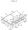
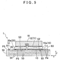
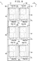
- the element mounting surface S1 is formed in the outer surface of the first smoothing capacitor 50.
- the first smoothing capacitor 50 has an outer shape of a cuboid, and the planar element mounting surface S1 is formed in the upper surface as the upper outer surface of the first smoothing capacitor 50 (the surface facing in the Z direction).
- the element mounting surface S1 is formed to have a rectangular shape as viewed in plan.
- capacitor connection electrodes P1, P2 as electrodes that are electrically connected to terminals of the first smoothing capacitor 50 are formed on the element mounting surface S1.
- the switching elements 10 are arranged (in other words, mounted) on the element mounting surface S1 such that terminals of the switching elements 10 are electrically connected to the capacitor connection electrodes P1, P2.
- the diode elements 20 electrically connected in parallel to the switching elements 10 are also arranged (in other words, mounted) on the element mounting surface S1 such that terminals of the diode elements 20 are electrically connected to the capacitor connection electrodes P1, P2.
- These switching elements 10 and diode elements 20 are arranged (i.e., placed) on the element mounting surface S1 or the electrodes formed on the element mounting surface S1 from above.
- the capacitor connection electrodes P1, P2 that are formed on the element mounting surface S1, and an inter-element connection electrode P3, a control electrode P4, and a discharge resistor electrode P5 which will be described below may be, e.g., electrodes made of conductive foil (copper foil etc.). Such electrodes can be formed on the element mounting surface S1 by using, e.g., a printing technique.
- the first smoothing capacitor 50 includes the first terminal 51 as a positive electrode-side terminal, and the second terminal 52 as a negative electrode-side terminal. These terminals 51, 52 function as input/output terminals of DC power between the DC power source 3 and the booster circuit 92, and also function as input/output terminals of DC power between the DC power source 3 and the inverter circuit 91.
- the first terminal 51 is placed at the end on the -X direction side of the first smoothing capacitor 50
- the second terminal 52 is placed at the end on the X direction side of the first smoothing capacitor 50. Both the first terminal 51 and the second terminal 52 are formed to be exposed on the upper surface of the first smoothing capacitor 50.
- the upper surface of the first smoothing capacitor 50 includes a portion that is formed by the upper end of the first terminal 51 and a portion that is formed by the upper end of the second terminal 52.
- the first terminal 51 is formed so as to be exposed on the side surface on the -X direction side of the first smoothing capacitor 50 (the outer surface on the lateral side; the same applies to the following description) and to be exposed on the side surfaces on both Y and -Y direction sides of the first smoothing capacitor 50.
- the second terminal 52 is formed to be exposed on the side surface on the X direction side of the first smoothing capacitor 50 and to be exposed on the side surfaces on both Y and -Y direction sides of the first smoothing capacitor 50.
- each dielectric portion 53 interposed between electrodes of the first smoothing capacitor 50 serves as a ceramic capacitor made of a ceramic material.
- This ceramic material is, e.g., barium titanate, strontium titanate, alumina.
- the first smoothing capacitor 50 is a stacked ceramic capacitor, and has a structure in which the dielectric portions 53 are stacked in the stacking direction (in this example, the vertical direction) with an internal electrode 54 interposed therebetween.
- the internal electrode 54 positive electrode-side internal electrodes 54 electrically connected to the first terminal 51 and negative electrode-side internal electrodes 54 electrically connected to the second terminal 52 are alternately arranged in the stacking direction.
- the positive electrode-side internal electrodes 54 are formed to extend in the first smoothing capacitor 50 from the first terminal 51 in the X direction.
- the negative electrode-side internal electrodes 54 are formed to extend in the first smoothing capacitor 50 from the second terminal 52 toward in -X direction.
- the internal electrodes 54 are formed to extend parallel to the element mounting surface S1.
- Both the first terminal 51 and the second terminal 52 function as external electrodes, and are formed to extend along the entire length in the stacking direction of the first smoothing capacitor 50.
- the number of stacks of the dielectric portions 53 is "5" in FIGS. 4 and 5
- an actual number of stacks of the dielectric portions 53 may be any value.
- a capacitor in which the number of stacks of the dielectric portions 53 is 100 or more may be used as the first smoothing capacitor 50.
- the element mounting surface S1 formed in the outer surface of the first smoothing capacitor 50 is formed integrally with the dielectric portion 53.
- the upper surface of the first smoothing capacitor 50 (specifically, the portion excluding the terminals 51, 52) is formed by the dielectric portion 53 located at the upper end
- the lower surface as the lower outer surface of the first smoothing capacitor 50 (specifically, the portion excluding the terminals 51, 52) is formed by the dielectric portion 53 located at the lower end.
- the upper surface of the first smoothing capacitor 50 in which the element mounting surface S1 is formed (specifically, the upper surface excluding the terminals 51, 52) and the lower surface of the first smoothing capacitor 50 (specifically, the lower surface excluding the terminals 51, 52) are integrally formed by using the same material as the dielectric portions 53.
- Capacitors manufactured by using various known techniques can be used as such a first smoothing capacitor 50.
- a capacitor manufactured by low temperature co-firing by using a low temperature co-fired ceramics (LTCC) technique can be used as the first smoothing capacitor 50.
- the material of the electrodes that are formed on the element mounting surface S1 e.g., the capacitor connection electrodes P1, P2
- a capacitor manufactured by using a technique of forming a film by injecting an aerosol of fine particles may be used as the first smoothing capacitor 50.
- a capacitor manufactured by alternately forming the dielectric portions 53 and the inner electrodes 54 in the stacking direction by using the aerosol deposition technique can be used as the first smoothing capacitor 50.
- the electrodes that are formed on the element mounting surface S1 e.g., the capacitor connection electrodes P1, P2
- the electrodes that are formed on the element mounting surface S1 e.g., the capacitor connection electrodes P1, P2
- fine particles of one or more of Al 2 O 3 , AlN, Si 3 N 4 , BN, MgO, and BaTiO 3 may be used as the fine particles forming the dielectric portions 53.
- the dielectric portions 53 may be formed by using alumina fine particles (an example of ceramic fine particles).
- fine particles of a material such as Cu or Ag may be used as the fine particles forming the internal electrodes 54.
- a switching element series circuit 70 that is formed by the switching elements 10 included in the switching element unit 1 will be described. As shown in FIGS. 2 and 3 , in the present embodiment, two switching elements 10 are placed on the element mounting surface S1. As described below, the switching element series circuit 70 shown in FIG. 7 is formed by electrically connecting these two switching elements 10 in series with each other. In other words, the two switching elements 10 forming the switching element series circuit 70 are placed on the same element mounting surface S1.
- the switching element series circuit 70 includes a first end 71 that is connected to the positive electrode side of the DC power source 3, and a second end 72 that is connected to the negative electrode side of the DC power source 3 (e.g., the ground side).
- the first end 71 of the switching element series circuit 70 is electrically connected to the positive electrode of the DC power source 3 via the switching elements 10 and the reactor 82 of the booster circuit 92, so that the DC voltage boosted by the booster circuit 92 is supplied to the first end 71 of the switching element series circuit 70.
- the switching element series circuit 70 forms one leg (a set of upper and lower arms) of the inverter circuit 91 that converts a DC voltage to an AC voltage.
- the rotating electrical machine 2 to which the AC voltage is to be supplied is an AC electric motor that is driven by a three-phase alternating current
- the inverter circuit 91 is formed by electrically connecting in parallel a total of three legs (arm sets) respectively corresponding to the three phases (U phase, V phase, and W phase).
- U phase, V phase, and W phase three phases
- W phase three phases
- one first smoothing capacitor 50 is electrically connected in parallel to each leg (each switching element series circuit 70).
- FIG. 7 shows an example in which one first smoothing capacitor 50 is connected to the three legs.
- the rotating electrical machine 2 to be controlled by the inverter circuit 91 may be, e.g., a rotating electrical machine that is provided as a driving force source of wheels in electric vehicles, hybrid vehicles.
- the term "rotating electrical machine” is used as a concept including a motor (electric motor), a generator (electric generator), and a motor generator that functions both as a motor and a generator as necessary.
- the first end 71 of the switching element series circuit 70 is electrically connected to the first terminal 51 as a positive electrode-side terminal of the first smoothing capacitor 50
- the second end 72 of the switching element series circuit 70 is electrically connected to the second terminal 52 as a negative electrode-side terminal of the first smoothing capacitor 50.
- the diode elements 20 are electrically connected in parallel to the two switching elements 10 of the switching element series circuit 70, respectively.
- the configuration of the switching element unit 1, which implements such an electric connection configuration, will be described below.
- the capacitor connection electrodes P1, P2 electrically connected to the terminals 51, 52 of the first smoothing capacitor 50 are formed on the element mounting surface S1.
- the first capacitor connection electrode P1 electrically connected to the first terminal 51 and the second capacitor connection electrode P2 electrically connected to the second terminal 52 are formed on the element mounting surface S1.
- the discharge resistor electrode P5 having both a portion electrically connected to the first terminal 51 and a portion electrically connected to the second terminal 52 is also formed on the element mounting surface S1.
- Each of the first capacitor connection electrode P1 and the portion of the discharge resistor electrode P5 which is electrically connected to the first terminal 51 is formed so as to cover a part of the upper surface of the first terminal 51, and thus is electrically connected to the first terminal 51.
- Each of the second capacitor connection electrode P2 and the portion of the discharge resistor electrode P5 which is electrically connected to the second terminal 52 is formed so as to cover a part of the upper surface of the second terminal 52, and thus is electrically connected to the second terminal 52.
- the first capacitor connection electrode P1 and the second capacitor connection electrode P2 are electrodes that electrically connect the switching element 10 and the first smoothing capacitor 50.
- the connection portions to an inverter circuit 91 side in the external electrodes of the first smoothing capacitor 50 are formed by the upper surfaces of the first terminal 51 and the second terminal 52.
- the connection portions to a DC power source 3 side in the external electrodes of the first smoothing capacitor 50 can also be formed by the upper surfaces of the first terminal 51 and the second terminal 52.
- the connection portions to the DC power source 3 side in the external electrodes of the first smoothing capacitor 50 may be formed by the side surfaces or the lower surfaces of the first terminal 51 and the second terminal 52.
- the inter-element connection electrode P3 and the control electrode P4 in addition to the three electrodes P1, P2, P5 are formed on the element mounting surface S1.
- These electrodes P3, P4 are electrodes that are electrically isolated from the terminals 51, 52 of the first smoothing capacitor 50.
- the expression "electrically isolated” means that the electrodes are electrically isolated on the element mounting surface S1, and is used as a conception including the case where the electrodes are electrically connected to the terminals of the first smoothing capacitor 50 via a circuit element, an interconnect member, etc. that is placed on the element mounting surface S1.
- the inter-element connection electrode P3 is placed between the first capacitor connection electrode P1 and the second capacitor connection electrode P2 in the extending direction of the element mounting surface S1 (in this example, the X direction).
- the first capacitor connection electrode P1, the second capacitor connection electrode P2, and the inter-element connection electrode P3 are formed to have an overlapping portion as viewed in the X direction. That is, there is a region in the Y direction, which is included in all of the following three regions. A region in the Y direction where the first capacitor connection electrode P1 is formed, a region in the Y direction where the second capacitor connection electrode P2 is formed, and a region in the Y direction where the inter-element connection electrode P3 is formed.
- the inter-element connection electrode P3 is formed to be interposed between the first capacitor connection electrode P1 and the second capacitor connection electrode P2 from both sides in the X direction.
- Each of these three electrodes P1 to P3 is formed in a rectangular shape.
- the inter-element connection electrode P3 in a part on the X-direction side of the inter-element connection electrode P3 where a second connection member 62 (described below) is placed, the inter-element connection electrode P3 has a portion that protrudes in the -Y direction from the rectangular portion.
- a connection member (not shown) connected to a coil of the rotating electrical machine 2 is connected to this protruding portion.
- the two switching elements 10 forming the switching element series circuit 70 are arranged next to each other in the X direction on the element mounting surface S1.
- the element mounting surface S1 is formed in a rectangular shape having longer and shorter sides such that the X direction is parallel to the extending direction of the longer sides and the Y direction is parallel to the extending direction of the shorter sides.
- the diode element 20 electrically connected in parallel to the switching element 10 is placed next to this switching element 10 in the Y direction on the element mounting surface S1. Specifically, the diode element 20 is placed on the Y direction side of the switching element 10 to be connected to this diode element 20, so as to adjoin this switching element 10.
- the expression "placed so as to adjoin” means that no other circuit element is located between the switching element 10 and the diode element 20 in the extending direction of the element mounting surface S1 (in this example, the Y direction), and is used as a concept including both the state where the separation distance between the switching element 10 and the diode element 20 is zero (that is, the state where the respective outer surfaces are in contact with each other) and the state where the separation distance is larger than zero.
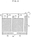
- the switching element 10 includes a pair of main terminals 12, 13 and a control terminal 11.
- the main terminals 12, 13 are terminals that are electrically connected to a DC voltage supply source (in this example, the DC power source 3).
- the positive electrode-side main terminal 12 is the terminal on the high potential side
- the negative electrode-side main terminal 13 is the terminal on the low potential side.
- the diode element 20 is electrically connected to the switching element 10 in an antiparallel relation so that a cathode terminal is electrically connected to the positive electrode-side main terminal 12 and an anode terminal is electrically connected to the negative electrode-side main terminal 13. That is, the diode element 20 functions as a free wheel diode (FWD).
- FWD free wheel diode
- the control terminal 11 is a control terminal that controls switching of the switching element 10.
- the switching element 10 When the switching element 10 is on, electric connection is obtained between the positive electrode-side main terminal 12 and the negative electrode-side main terminal 13.
- the switching element 10 When the switching element 10 is off, the electric connection between the positive electrode-side main terminal 12 and the negative electrode-side main terminal 13 is cut off.
- the positive electrode-side main terminal 12 of the upper stage switching element 10a that is located on the high potential side in the two switching elements 10 is electrically connected to the first end 71 of the switching element series circuit 70. That is, the upper stage switching element 10a is one of the two switching elements 10 of the switching element series circuit 70, which is located on a first end 71 side.
- the negative electrode-side main terminal 13 of the lower stage switching element 10b that is located on the low potential side in the two switching elements 10 is electrically connected to the second end 72 of the switching element series circuit 70. That is, the lower stage switching element 10b is one of the two switching elements 10 of the switching element series circuit 70, which is located on a second end 72 side.
- connection point between the negative electrode-side main terminal 13 of the upper stage switching element 10a and the positive electrode-side main terminal 12 of the lower stage switching element 10b (the series connection point of the switching element series circuit 70) is electrically connected to the coil of the rotating electrical machine 2.
- the upper stage switching element 10a corresponds to the "first switching element” in the present invention
- the lower stage switching element 10b corresponds to the "second switching element” in the present invention.
- the switching element 10 is an insulated gate bipolar transistor (IGBT), in which the positive electrode-side main terminal 12 is formed by a collector terminal, the negative electrode-side main terminal 13 is formed by an emitter terminal, and the control terminal 11 is formed by a gate terminal.
- the control terminal 11 is electrically connected to a control unit, not shown, via a gate resistor 83 (see FIGS. 3 and 5 ), and switching of each switching element 10 is individually controlled according to the gate voltage that is applied to the control terminal 11.
- MOSFETs Metal oxide semiconductor field effect transistors
- the positive electrode-side main terminal 12 and the negative electrode-side main terminal 13 are separately formed on the outer surfaces of the switching element 10 which face opposite sides to each other.
- the switching element 10 has an outer surface having the positive electrode-side main terminal 12 formed thereon, and an outer surface having the negative electrode-side main terminal 13 formed thereon, and these two outer surfaces face in the opposite directions to each other and are parallel to each other.
- the switching element 10 is placed on the element mounting surface S1 so that the outer surface having the negative electrode-side main terminal 13 formed thereon serves as a first opposing mounting surface S2 facing the element mounting surface S1.
- the control terminal 11 is located at an insulation distance from the negative electrode-side main terminal 13 on the outer surface of the switching element 10 having the negative electrode-side main terminal 13 formed thereon. That is, in the present embodiment, the main terminal 12, 13 (specifically, the negative electrode-side main terminal 13) is formed on the first opposing mounting surface S2 of the switching element 10. In the present embodiment, the control terminal 11 is also formed on the first opposing mounting surface S2.
- the switching element 10 is placed on the element mounting surface S1 so that the first opposing mounting surface S2 contacts the element mounting surface S1 directly or via a bonding member.
- the element mounting surface S1 in the expression "contacts the element mounting surface S1 directly or via a bonding member” includes the electrodes formed on the element mounting surface S1.
- the upper stage switching element 10a is placed from above on the inter-element connection electrode P3 via a bonding material 93, and an upper stage diode element 20a as the diode element 20 electrically connected in parallel to the upper stage switching element 10a is also placed from above on the inter-element connection electrode P3 via the bonding material 93.
- the anode terminal is formed on the lower surface of the diode element 20, and the cathode terminal is formed on the upper surface of the diode element 20. That is, the lower surface of the diode element 20 serves as a second opposing mounting surface S3 facing the element mounting surface S1, and the diode element 20 is placed over the element mounting surface S1 so that the second opposing mounting surface S3 contacts the element mounting surface S1 directly or via the bonding member.
- the anode terminal is formed on the second opposing mounting surface S3.
- the bonding material 93 is comprised of a conductive material such as, e.g., solder or conductive paste.
- the negative electrode-side main terminal 13 formed on the lower surface of the upper stage switching element 10a and the anode terminal formed on the lower surface of the upper stage diode element 20a are electrically connected to the inter-element connection electrode P3.
- the bonding material 93 corresponds to the "bonding member" in the present invention.
- the lower stage switching element 10b is placed from above on the second capacitor connection electrode P2 via the bonding material 93.
- a lower stage diode element 20b as the diode element 20 electrically connected in parallel to the lower stage switching element 10b is also placed from above on the second capacitor connection electrode P2 via the bonding material 93.
- the negative electrode-side main terminal 13 formed on the lower surface of the lower stage switching element 10b and the anode terminal formed on the lower surface of the lower stage diode element 20b are electrically connected to the second capacitor connection electrode P2.
- the second capacitor connection electrode P2 is electrically connected to the second terminal 52, and the negative electrode-side main terminal 13 of the lower stage switching element 10b and the anode terminal of the lower stage diode element 20b are electrically connected to the second terminal 52 via the second capacitor connection electrode P2.
- the second capacitor connection electrode P2 is an electrode that electrically connects the second end 72 of the switching element series circuit 70 formed by the negative electrode-side main terminal 13 of the lower stage switching element 10b to the second terminal 52 of the first smoothing capacitor 50.
- a conductive first connection member 61 is placed so as to electrically connect the positive electrode-side main terminal 12 (see FIGS. 4 and 5 ) formed on the upper surface of the upper stage switching element 10a and the cathode terminal formed on the upper surface of the upper stage diode element 20a to the first capacitor connection electrode P1. That is, the first connection member 61 electrically connects the first capacitor connection electrode P1 and the upper stage switching element 10a. Specifically, as shown in FIG.
- the first connection member 61 has a first portion 61a placed from above on the first capacitor connection electrode P1 via the bonding material 93, and a second portion 61b placed from above on the upper stage switching element 10a and the upper stage diode element 20a via the bonding material 93. That is, the first portion 61a is a portion of the first connection member 61 which contacts the first capacitor connection electrode P1 directly or via the bonding member.
- the second portion 61b is a portion of the first connection member 61 which contacts the upper stage switching element 10a directly or via the bonding member. In the present embodiment, the second portion 61b is also a portion that contacts the upper stage diode element 20a directly or via the bonding member.
- the positive electrode-side main terminal 12 of the upper stage switching element 10a and the cathode terminal of the upper stage diode element 20a are electrically connected to the first capacitor connection electrode P1.
- the first capacitor connection electrode P1 is electrically connected to the first terminal 51, and the positive electrode-side main terminal 12 of the upper stage switching element 10a and the cathode terminal of the upper stage diode element 20a are electrically connected to the first terminal 51 via the first capacitor connection electrode P1.
- the first capacitor connection electrode P1 is an electrode that electrically connects the first end 71 of the switching element series circuit 70, which is formed by the positive electrode-side main terminal 12 of the upper stage switching element 10a, to the first terminal 51 of the first smoothing capacitor 50.
- the conductive second connection member 62 is placed so as to electrically connect the positive electrode-side main terminal 12 (see FIG. 4 ) formed on the upper surface of the lower stage switching element 10b and the cathode terminal formed on the upper surface of the lower stage diode element 20b to the inter-element connection electrode P3. That is, the second connection member 62 electrically connects the inter-element connection electrode P3 and the lower stage switching element 10b. Specifically, as shown in FIG.
- the second connection member 62 has a first portion 62a placed from above on the inter-element connection electrode P3 via the bonding material 93, and a second portion 62b placed from above on the lower stage switching element 10b and the lower stage diode element 20b via the bonding material 93. That is, the first portion 62a is a portion of the second connection member 62 which contacts the inter-element connection electrode P3 directly or via the bonding member.
- the second portion 62b is a portion of the second connection member 62 which contacts the lower stage switching element 10b directly or via the bonding member. In the present embodiment, the second portion 62b is also a portion that contacts the lower stage diode element 20b directly or via the bonding member.
- the positive electrode-side main terminal 12 of the lower stage switching element 10b and the cathode terminal of the lower stage diode element 20b are electrically connected to the inter-element connection electrode P3.
- the negative electrode-side main terminal 13 of the upper stage switching element 10a and the anode terminal of the upper stage diode element 20a are electrically connected to the positive electrode-side main terminal 12 of the lower stage switching element 10b and the cathode terminal of the lower stage diode element 20b via the inter-element connection electrode P3.
- the inter-element connection electrode P3 is an electrode that electrically connects the two switching terminals 10 (specifically, the upper stage switching element 10a and the lower stage switching element 10b).
- each of the first connection member 61 and the second connection member 62 has a flat portion in its upper surface.
- a heat sink is placed on the upper side of the flat portion with an insulating member interposed therebetween.
- This insulating member has both an electrical insulation property and a heat conductive property. This allows the heat of the switching element 10 to be efficiently transmitted to the heat sink via the connection members 61, 62 while ensuring electrical insulation between the switching element 10 and the heat sink.
- the connection members 61, 62 have a function as a heat spreader in addition to the function as a connection member (bus bar).
- the control electrode P4 is a control electrode that is electrically connected to the control terminal 11. As shown in FIG. 5 , the control electrode P4 has a portion that is located below the control terminal 11 and electrically connected to the control terminal 11, and a portion separated from this portion in the -Y direction (a separated portion). The gate resistor 83 is placed from above on the control electrode P4 so as to electrically connect these two portions. Although not shown in the figures, a connection terminal of a flexible printed board is formed in the separated portion, and the control terminal 11 is electrically connected to a control unit (not shown) that generates a switching control signal (in this example, a gate drive signal) via the flexible printed board.
- the flexible printed board is a printed board that is flexible and is deformable to a large extent.
- the discharge resistor electrode P5 is an electrode on which the discharge resistor 81 (see FIG. 7 ) electrically connected in parallel to the first smoothing capacitor 50 is placed. Specifically, as shown in FIG. 6 , the discharge resistor electrode P5 has two portions that are separated from each other in the X direction, namely, a portion electrically connected to the first terminal 51 and a portion electrically connected to the second terminal 52. As shown in FIG. 1 , the discharge resistor 81 is placed from above on the discharge resistor electrode P5 so as to electrically connect these two portions.
- the present invention can be preferably used in switching element units having switching elements.
Landscapes
- Engineering & Computer Science (AREA)
- Power Engineering (AREA)
- Microelectronics & Electronic Packaging (AREA)
- Computer Hardware Design (AREA)
- Physics & Mathematics (AREA)
- Condensed Matter Physics & Semiconductors (AREA)
- General Physics & Mathematics (AREA)
- Inverter Devices (AREA)
- General Engineering & Computer Science (AREA)
Applications Claiming Priority (3)
| Application Number | Priority Date | Filing Date | Title |
|---|---|---|---|
| JP2012019132 | 2012-01-31 | ||
| JP2012263052A JP5935672B2 (ja) | 2012-01-31 | 2012-11-30 | スイッチング素子ユニット |
| PCT/JP2013/052429 WO2013115395A1 (en) | 2012-01-31 | 2013-01-29 | Switching element unit |
Publications (2)
| Publication Number | Publication Date |
|---|---|
| EP2766930A1 EP2766930A1 (en) | 2014-08-20 |
| EP2766930B1 true EP2766930B1 (en) | 2018-04-04 |
Family
ID=47754926
Family Applications (1)
| Application Number | Title | Priority Date | Filing Date |
|---|---|---|---|
| EP13706754.2A Not-in-force EP2766930B1 (en) | 2012-01-31 | 2013-01-29 | Switching element unit |
Country Status (6)
| Country | Link |
|---|---|
| US (1) | US9177948B2 (enExample) |
| EP (1) | EP2766930B1 (enExample) |
| JP (1) | JP5935672B2 (enExample) |
| KR (1) | KR101691707B1 (enExample) |
| CN (1) | CN104160501B (enExample) |
| WO (1) | WO2013115395A1 (enExample) |
Families Citing this family (10)
| Publication number | Priority date | Publication date | Assignee | Title |
|---|---|---|---|---|
| JP2014029944A (ja) * | 2012-07-31 | 2014-02-13 | Aisin Aw Co Ltd | スイッチング素子ユニット |
| JP2015060991A (ja) * | 2013-09-19 | 2015-03-30 | パナソニックIpマネジメント株式会社 | 半導体装置及びそれを用いた半導体リレー |
| JP2015191902A (ja) * | 2014-03-27 | 2015-11-02 | トヨタ自動車株式会社 | 半導体モジュール |
| DE102014111421A1 (de) * | 2014-08-11 | 2016-02-11 | Woodward Kempen Gmbh | Niederinduktive Schaltungsanordnung eines Umrichters |
| JP6361447B2 (ja) * | 2014-10-15 | 2018-07-25 | 住友電気工業株式会社 | 半導体モジュール |
| CN107078126B (zh) * | 2014-11-06 | 2020-10-02 | 三菱电机株式会社 | 半导体模块以及半导体模块用的导电构件 |
| US9681568B1 (en) * | 2015-12-02 | 2017-06-13 | Ge Energy Power Conversion Technology Ltd | Compact stacked power modules for minimizing commutating inductance and methods for making the same |
| DE102018124695A1 (de) * | 2017-11-15 | 2019-05-16 | Taiwan Semiconductor Manufacturing Co., Ltd. | Integrieren von Passivvorrichtungen in Package-Strukturen |
| WO2022097533A1 (ja) * | 2020-11-09 | 2022-05-12 | ローム株式会社 | 放電回路モジュール |
| DE102022208266A1 (de) * | 2022-08-09 | 2024-02-15 | Magna powertrain gmbh & co kg | Leistungsmodul mit flexibler Leiterplatte |
Family Cites Families (16)
| Publication number | Priority date | Publication date | Assignee | Title |
|---|---|---|---|---|
| JPS5961917A (ja) * | 1982-10-01 | 1984-04-09 | 松下電器産業株式会社 | 複合電子部品 |
| US5095402A (en) * | 1990-10-02 | 1992-03-10 | Rogers Corporation | Internally decoupled integrated circuit package |
| JPH05152161A (ja) * | 1992-02-10 | 1993-06-18 | Tdk Corp | 複合部品 |
| JPH08181445A (ja) | 1994-12-22 | 1996-07-12 | Sumitomo Metal Ind Ltd | セラミックス多層基板 |
| JPH11178353A (ja) | 1997-12-11 | 1999-07-02 | Hitachi Ltd | 共振形インバータ及びそれを用いた電気車 |
| US6373127B1 (en) * | 1998-09-29 | 2002-04-16 | Texas Instruments Incorporated | Integrated capacitor on the back of a chip |
| US6940164B1 (en) * | 2000-08-18 | 2005-09-06 | Mitsubishi Denki Kabushiki Kaisha | Power module |
| JP2002176128A (ja) * | 2000-12-06 | 2002-06-21 | Toyota Motor Corp | マルチチップモジュールの冷却構造 |
| JP3847676B2 (ja) * | 2002-07-15 | 2006-11-22 | 三菱電機株式会社 | パワー半導体装置 |
| US6987670B2 (en) * | 2003-05-16 | 2006-01-17 | Ballard Power Systems Corporation | Dual power module power system architecture |
| US7443692B2 (en) * | 2003-05-16 | 2008-10-28 | Continental Automotive Systems Us, Inc. | Power converter architecture employing at least one capacitor across a DC bus |
| JP4038455B2 (ja) * | 2003-08-21 | 2008-01-23 | 三菱電機株式会社 | 半導体装置 |
| JP2006190972A (ja) | 2004-12-08 | 2006-07-20 | Mitsubishi Electric Corp | 電力用半導体装置 |
| JP4661645B2 (ja) * | 2005-03-23 | 2011-03-30 | トヨタ自動車株式会社 | パワー半導体モジュール |
| JP4651653B2 (ja) * | 2007-10-15 | 2011-03-16 | 三菱電機株式会社 | 電力変換装置 |
| US8253241B2 (en) * | 2008-05-20 | 2012-08-28 | Infineon Technologies Ag | Electronic module |
-
2012
- 2012-11-30 JP JP2012263052A patent/JP5935672B2/ja not_active Expired - Fee Related
-
2013
- 2013-01-29 CN CN201380004115.1A patent/CN104160501B/zh not_active Expired - Fee Related
- 2013-01-29 EP EP13706754.2A patent/EP2766930B1/en not_active Not-in-force
- 2013-01-29 US US14/359,486 patent/US9177948B2/en not_active Expired - Fee Related
- 2013-01-29 WO PCT/JP2013/052429 patent/WO2013115395A1/en not_active Ceased
- 2013-01-29 KR KR1020147014786A patent/KR101691707B1/ko not_active Expired - Fee Related
Also Published As
| Publication number | Publication date |
|---|---|
| JP2013179261A (ja) | 2013-09-09 |
| KR101691707B1 (ko) | 2016-12-30 |
| US20140264519A1 (en) | 2014-09-18 |
| WO2013115395A1 (en) | 2013-08-08 |
| JP5935672B2 (ja) | 2016-06-15 |
| EP2766930A1 (en) | 2014-08-20 |
| KR20140090228A (ko) | 2014-07-16 |
| CN104160501B (zh) | 2016-11-09 |
| CN104160501A (zh) | 2014-11-19 |
| US9177948B2 (en) | 2015-11-03 |
Similar Documents
| Publication | Publication Date | Title |
|---|---|---|
| EP2766930B1 (en) | Switching element unit | |
| US11532538B2 (en) | Component structure, power module and power module assembly structure | |
| JP6160780B2 (ja) | 3レベル電力変換装置 | |
| US11538794B2 (en) | Power converter with an upper arm and a lower arm and at least first and second semiconductor devices connected by a bridging member | |
| US20150326221A1 (en) | Switching element unit | |
| CN102754327B (zh) | 电力变换装置 | |
| EP2264894A1 (en) | Power module with additional transient current path and power module system | |
| US8526189B2 (en) | Power module | |
| US20150195957A1 (en) | Electric power convertor | |
| JP3622782B2 (ja) | 半導体装置 | |
| CN110178304B (zh) | 半导体装置 | |
| US10027094B2 (en) | Power module, power converter and drive arrangement with a power module | |
| JP6053668B2 (ja) | 半導体モジュールおよび電力変換装置 | |
| CN111211114A (zh) | 一种快速功率模块及功率模组 | |
| JP2015053410A (ja) | 半導体モジュール | |
| CN1917203B (zh) | 具有线路元件的功率半导体模块 | |
| JP2014072344A (ja) | 平滑コンデンサ | |
| JP2005191233A (ja) | パワーモジュール | |
| JP2024015805A (ja) | スイッチングデバイスおよびスイッチングモジュール | |
| US12388375B2 (en) | Switching module including heat radiation member and inverter including the same | |
| CN116941035A (zh) | 功率半导体装置以及电力转换装置 |
Legal Events
| Date | Code | Title | Description |
|---|---|---|---|
| PUAI | Public reference made under article 153(3) epc to a published international application that has entered the european phase |
Free format text: ORIGINAL CODE: 0009012 |
|
| 17P | Request for examination filed |
Effective date: 20140513 |
|
| AK | Designated contracting states |
Kind code of ref document: A1 Designated state(s): AL AT BE BG CH CY CZ DE DK EE ES FI FR GB GR HR HU IE IS IT LI LT LU LV MC MK MT NL NO PL PT RO RS SE SI SK SM TR |
|
| DAX | Request for extension of the european patent (deleted) | ||
| REG | Reference to a national code |
Ref country code: DE Ref legal event code: R079 Ref document number: 602013035347 Country of ref document: DE Free format text: PREVIOUS MAIN CLASS: H01L0025000000 Ipc: H01L0023000000 |
|
| RIC1 | Information provided on ipc code assigned before grant |
Ipc: H02M 1/12 20060101ALI20170120BHEP Ipc: H01L 23/00 20060101AFI20170120BHEP Ipc: H02M 7/00 20060101ALI20170120BHEP |
|
| GRAP | Despatch of communication of intention to grant a patent |
Free format text: ORIGINAL CODE: EPIDOSNIGR1 |
|
| STAA | Information on the status of an ep patent application or granted ep patent |
Free format text: STATUS: GRANT OF PATENT IS INTENDED |
|
| INTG | Intention to grant announced |
Effective date: 20171206 |
|
| GRAS | Grant fee paid |
Free format text: ORIGINAL CODE: EPIDOSNIGR3 |
|
| GRAA | (expected) grant |
Free format text: ORIGINAL CODE: 0009210 |
|
| STAA | Information on the status of an ep patent application or granted ep patent |
Free format text: STATUS: THE PATENT HAS BEEN GRANTED |
|
| AK | Designated contracting states |
Kind code of ref document: B1 Designated state(s): AL AT BE BG CH CY CZ DE DK EE ES FI FR GB GR HR HU IE IS IT LI LT LU LV MC MK MT NL NO PL PT RO RS SE SI SK SM TR |
|
| REG | Reference to a national code |
Ref country code: GB Ref legal event code: FG4D |
|
| REG | Reference to a national code |
Ref country code: CH Ref legal event code: EP |
|
| REG | Reference to a national code |
Ref country code: AT Ref legal event code: REF Ref document number: 986463 Country of ref document: AT Kind code of ref document: T Effective date: 20180415 |
|
| REG | Reference to a national code |
Ref country code: IE Ref legal event code: FG4D |
|
| REG | Reference to a national code |
Ref country code: DE Ref legal event code: R096 Ref document number: 602013035347 Country of ref document: DE |
|
| REG | Reference to a national code |
Ref country code: NL Ref legal event code: MP Effective date: 20180404 |
|
| REG | Reference to a national code |
Ref country code: LT Ref legal event code: MG4D |
|
| PG25 | Lapsed in a contracting state [announced via postgrant information from national office to epo] |
Ref country code: NL Free format text: LAPSE BECAUSE OF FAILURE TO SUBMIT A TRANSLATION OF THE DESCRIPTION OR TO PAY THE FEE WITHIN THE PRESCRIBED TIME-LIMIT Effective date: 20180404 |
|
| PG25 | Lapsed in a contracting state [announced via postgrant information from national office to epo] |
Ref country code: LT Free format text: LAPSE BECAUSE OF FAILURE TO SUBMIT A TRANSLATION OF THE DESCRIPTION OR TO PAY THE FEE WITHIN THE PRESCRIBED TIME-LIMIT Effective date: 20180404 Ref country code: NO Free format text: LAPSE BECAUSE OF FAILURE TO SUBMIT A TRANSLATION OF THE DESCRIPTION OR TO PAY THE FEE WITHIN THE PRESCRIBED TIME-LIMIT Effective date: 20180704 Ref country code: BG Free format text: LAPSE BECAUSE OF FAILURE TO SUBMIT A TRANSLATION OF THE DESCRIPTION OR TO PAY THE FEE WITHIN THE PRESCRIBED TIME-LIMIT Effective date: 20180704 Ref country code: FI Free format text: LAPSE BECAUSE OF FAILURE TO SUBMIT A TRANSLATION OF THE DESCRIPTION OR TO PAY THE FEE WITHIN THE PRESCRIBED TIME-LIMIT Effective date: 20180404 Ref country code: SE Free format text: LAPSE BECAUSE OF FAILURE TO SUBMIT A TRANSLATION OF THE DESCRIPTION OR TO PAY THE FEE WITHIN THE PRESCRIBED TIME-LIMIT Effective date: 20180404 Ref country code: PL Free format text: LAPSE BECAUSE OF FAILURE TO SUBMIT A TRANSLATION OF THE DESCRIPTION OR TO PAY THE FEE WITHIN THE PRESCRIBED TIME-LIMIT Effective date: 20180404 Ref country code: ES Free format text: LAPSE BECAUSE OF FAILURE TO SUBMIT A TRANSLATION OF THE DESCRIPTION OR TO PAY THE FEE WITHIN THE PRESCRIBED TIME-LIMIT Effective date: 20180404 Ref country code: AL Free format text: LAPSE BECAUSE OF FAILURE TO SUBMIT A TRANSLATION OF THE DESCRIPTION OR TO PAY THE FEE WITHIN THE PRESCRIBED TIME-LIMIT Effective date: 20180404 |
|
| PG25 | Lapsed in a contracting state [announced via postgrant information from national office to epo] |
Ref country code: LV Free format text: LAPSE BECAUSE OF FAILURE TO SUBMIT A TRANSLATION OF THE DESCRIPTION OR TO PAY THE FEE WITHIN THE PRESCRIBED TIME-LIMIT Effective date: 20180404 Ref country code: GR Free format text: LAPSE BECAUSE OF FAILURE TO SUBMIT A TRANSLATION OF THE DESCRIPTION OR TO PAY THE FEE WITHIN THE PRESCRIBED TIME-LIMIT Effective date: 20180705 Ref country code: HR Free format text: LAPSE BECAUSE OF FAILURE TO SUBMIT A TRANSLATION OF THE DESCRIPTION OR TO PAY THE FEE WITHIN THE PRESCRIBED TIME-LIMIT Effective date: 20180404 Ref country code: RS Free format text: LAPSE BECAUSE OF FAILURE TO SUBMIT A TRANSLATION OF THE DESCRIPTION OR TO PAY THE FEE WITHIN THE PRESCRIBED TIME-LIMIT Effective date: 20180404 |
|
| REG | Reference to a national code |
Ref country code: AT Ref legal event code: MK05 Ref document number: 986463 Country of ref document: AT Kind code of ref document: T Effective date: 20180404 |
|
| PG25 | Lapsed in a contracting state [announced via postgrant information from national office to epo] |
Ref country code: PT Free format text: LAPSE BECAUSE OF FAILURE TO SUBMIT A TRANSLATION OF THE DESCRIPTION OR TO PAY THE FEE WITHIN THE PRESCRIBED TIME-LIMIT Effective date: 20180806 |
|
| REG | Reference to a national code |
Ref country code: DE Ref legal event code: R097 Ref document number: 602013035347 Country of ref document: DE |
|
| PG25 | Lapsed in a contracting state [announced via postgrant information from national office to epo] |
Ref country code: AT Free format text: LAPSE BECAUSE OF FAILURE TO SUBMIT A TRANSLATION OF THE DESCRIPTION OR TO PAY THE FEE WITHIN THE PRESCRIBED TIME-LIMIT Effective date: 20180404 Ref country code: EE Free format text: LAPSE BECAUSE OF FAILURE TO SUBMIT A TRANSLATION OF THE DESCRIPTION OR TO PAY THE FEE WITHIN THE PRESCRIBED TIME-LIMIT Effective date: 20180404 Ref country code: DK Free format text: LAPSE BECAUSE OF FAILURE TO SUBMIT A TRANSLATION OF THE DESCRIPTION OR TO PAY THE FEE WITHIN THE PRESCRIBED TIME-LIMIT Effective date: 20180404 Ref country code: SK Free format text: LAPSE BECAUSE OF FAILURE TO SUBMIT A TRANSLATION OF THE DESCRIPTION OR TO PAY THE FEE WITHIN THE PRESCRIBED TIME-LIMIT Effective date: 20180404 Ref country code: RO Free format text: LAPSE BECAUSE OF FAILURE TO SUBMIT A TRANSLATION OF THE DESCRIPTION OR TO PAY THE FEE WITHIN THE PRESCRIBED TIME-LIMIT Effective date: 20180404 Ref country code: CZ Free format text: LAPSE BECAUSE OF FAILURE TO SUBMIT A TRANSLATION OF THE DESCRIPTION OR TO PAY THE FEE WITHIN THE PRESCRIBED TIME-LIMIT Effective date: 20180404 |
|
| PLBE | No opposition filed within time limit |
Free format text: ORIGINAL CODE: 0009261 |
|
| STAA | Information on the status of an ep patent application or granted ep patent |
Free format text: STATUS: NO OPPOSITION FILED WITHIN TIME LIMIT |
|
| PG25 | Lapsed in a contracting state [announced via postgrant information from national office to epo] |
Ref country code: SM Free format text: LAPSE BECAUSE OF FAILURE TO SUBMIT A TRANSLATION OF THE DESCRIPTION OR TO PAY THE FEE WITHIN THE PRESCRIBED TIME-LIMIT Effective date: 20180404 Ref country code: IT Free format text: LAPSE BECAUSE OF FAILURE TO SUBMIT A TRANSLATION OF THE DESCRIPTION OR TO PAY THE FEE WITHIN THE PRESCRIBED TIME-LIMIT Effective date: 20180404 |
|
| 26N | No opposition filed |
Effective date: 20190107 |
|
| PG25 | Lapsed in a contracting state [announced via postgrant information from national office to epo] |
Ref country code: SI Free format text: LAPSE BECAUSE OF FAILURE TO SUBMIT A TRANSLATION OF THE DESCRIPTION OR TO PAY THE FEE WITHIN THE PRESCRIBED TIME-LIMIT Effective date: 20180404 |
|
| PG25 | Lapsed in a contracting state [announced via postgrant information from national office to epo] |
Ref country code: MC Free format text: LAPSE BECAUSE OF FAILURE TO SUBMIT A TRANSLATION OF THE DESCRIPTION OR TO PAY THE FEE WITHIN THE PRESCRIBED TIME-LIMIT Effective date: 20180404 |
|
| REG | Reference to a national code |
Ref country code: CH Ref legal event code: PL |
|
| PG25 | Lapsed in a contracting state [announced via postgrant information from national office to epo] |
Ref country code: LU Free format text: LAPSE BECAUSE OF NON-PAYMENT OF DUE FEES Effective date: 20190129 |
|
| REG | Reference to a national code |
Ref country code: BE Ref legal event code: MM Effective date: 20190131 |
|
| REG | Reference to a national code |
Ref country code: IE Ref legal event code: MM4A |
|
| PG25 | Lapsed in a contracting state [announced via postgrant information from national office to epo] |
Ref country code: BE Free format text: LAPSE BECAUSE OF NON-PAYMENT OF DUE FEES Effective date: 20190131 |
|
| PG25 | Lapsed in a contracting state [announced via postgrant information from national office to epo] |
Ref country code: CH Free format text: LAPSE BECAUSE OF NON-PAYMENT OF DUE FEES Effective date: 20190131 Ref country code: LI Free format text: LAPSE BECAUSE OF NON-PAYMENT OF DUE FEES Effective date: 20190131 |
|
| PG25 | Lapsed in a contracting state [announced via postgrant information from national office to epo] |
Ref country code: IE Free format text: LAPSE BECAUSE OF NON-PAYMENT OF DUE FEES Effective date: 20190129 |
|
| PGFP | Annual fee paid to national office [announced via postgrant information from national office to epo] |
Ref country code: FR Payment date: 20191216 Year of fee payment: 8 |
|
| PG25 | Lapsed in a contracting state [announced via postgrant information from national office to epo] |
Ref country code: TR Free format text: LAPSE BECAUSE OF FAILURE TO SUBMIT A TRANSLATION OF THE DESCRIPTION OR TO PAY THE FEE WITHIN THE PRESCRIBED TIME-LIMIT Effective date: 20180404 |
|
| PGFP | Annual fee paid to national office [announced via postgrant information from national office to epo] |
Ref country code: DE Payment date: 20200114 Year of fee payment: 8 Ref country code: GB Payment date: 20200122 Year of fee payment: 8 |
|
| PG25 | Lapsed in a contracting state [announced via postgrant information from national office to epo] |
Ref country code: MT Free format text: LAPSE BECAUSE OF NON-PAYMENT OF DUE FEES Effective date: 20190129 |
|
| PG25 | Lapsed in a contracting state [announced via postgrant information from national office to epo] |
Ref country code: CY Free format text: LAPSE BECAUSE OF FAILURE TO SUBMIT A TRANSLATION OF THE DESCRIPTION OR TO PAY THE FEE WITHIN THE PRESCRIBED TIME-LIMIT Effective date: 20180404 |
|
| PG25 | Lapsed in a contracting state [announced via postgrant information from national office to epo] |
Ref country code: IS Free format text: LAPSE BECAUSE OF FAILURE TO SUBMIT A TRANSLATION OF THE DESCRIPTION OR TO PAY THE FEE WITHIN THE PRESCRIBED TIME-LIMIT Effective date: 20180804 |
|
| PG25 | Lapsed in a contracting state [announced via postgrant information from national office to epo] |
Ref country code: HU Free format text: LAPSE BECAUSE OF FAILURE TO SUBMIT A TRANSLATION OF THE DESCRIPTION OR TO PAY THE FEE WITHIN THE PRESCRIBED TIME-LIMIT; INVALID AB INITIO Effective date: 20130129 |
|
| REG | Reference to a national code |
Ref country code: DE Ref legal event code: R119 Ref document number: 602013035347 Country of ref document: DE |
|
| GBPC | Gb: european patent ceased through non-payment of renewal fee |
Effective date: 20210129 |
|
| PG25 | Lapsed in a contracting state [announced via postgrant information from national office to epo] |
Ref country code: FR Free format text: LAPSE BECAUSE OF NON-PAYMENT OF DUE FEES Effective date: 20210131 |
|
| PG25 | Lapsed in a contracting state [announced via postgrant information from national office to epo] |
Ref country code: DE Free format text: LAPSE BECAUSE OF NON-PAYMENT OF DUE FEES Effective date: 20210803 Ref country code: GB Free format text: LAPSE BECAUSE OF NON-PAYMENT OF DUE FEES Effective date: 20210129 |
|
| PG25 | Lapsed in a contracting state [announced via postgrant information from national office to epo] |
Ref country code: MK Free format text: LAPSE BECAUSE OF FAILURE TO SUBMIT A TRANSLATION OF THE DESCRIPTION OR TO PAY THE FEE WITHIN THE PRESCRIBED TIME-LIMIT Effective date: 20180404 |