EP2709177B1 - Light emitting device - Google Patents
Light emitting device Download PDFInfo
- Publication number
- EP2709177B1 EP2709177B1 EP13178622.0A EP13178622A EP2709177B1 EP 2709177 B1 EP2709177 B1 EP 2709177B1 EP 13178622 A EP13178622 A EP 13178622A EP 2709177 B1 EP2709177 B1 EP 2709177B1
- Authority
- EP
- European Patent Office
- Prior art keywords
- light emitting
- layer
- disposed
- emitting chip
- electrode
- Prior art date
- Legal status (The legal status is an assumption and is not a legal conclusion. Google has not performed a legal analysis and makes no representation as to the accuracy of the status listed.)
- Active
Links
- 239000011347 resin Substances 0.000 claims description 100
- 229920005989 resin Polymers 0.000 claims description 100
- 239000004065 semiconductor Substances 0.000 claims description 69
- OAICVXFJPJFONN-UHFFFAOYSA-N Phosphorus Chemical compound [P] OAICVXFJPJFONN-UHFFFAOYSA-N 0.000 claims description 41
- 230000001681 protective effect Effects 0.000 claims description 35
- 229910044991 metal oxide Inorganic materials 0.000 claims description 25
- 150000004706 metal oxides Chemical class 0.000 claims description 25
- 239000010410 layer Substances 0.000 description 308
- 239000000758 substrate Substances 0.000 description 30
- 239000000463 material Substances 0.000 description 23
- 230000004888 barrier function Effects 0.000 description 11
- 229910052751 metal Inorganic materials 0.000 description 11
- 230000003287 optical effect Effects 0.000 description 11
- XLOMVQKBTHCTTD-UHFFFAOYSA-N Zinc monoxide Chemical compound [Zn]=O XLOMVQKBTHCTTD-UHFFFAOYSA-N 0.000 description 10
- 150000001875 compounds Chemical class 0.000 description 10
- 239000002019 doping agent Substances 0.000 description 10
- 239000002184 metal Substances 0.000 description 10
- -1 SiO2 Chemical class 0.000 description 9
- GWEVSGVZZGPLCZ-UHFFFAOYSA-N Titan oxide Chemical compound O=[Ti]=O GWEVSGVZZGPLCZ-UHFFFAOYSA-N 0.000 description 9
- 230000005855 radiation Effects 0.000 description 9
- VYPSYNLAJGMNEJ-UHFFFAOYSA-N Silicium dioxide Chemical compound O=[Si]=O VYPSYNLAJGMNEJ-UHFFFAOYSA-N 0.000 description 8
- 230000001070 adhesive effect Effects 0.000 description 8
- 229910052710 silicon Inorganic materials 0.000 description 8
- 229910052782 aluminium Inorganic materials 0.000 description 6
- 239000003822 epoxy resin Substances 0.000 description 6
- 239000004417 polycarbonate Substances 0.000 description 6
- 229920000647 polyepoxide Polymers 0.000 description 6
- 229910002704 AlGaN Inorganic materials 0.000 description 5
- XUIMIQQOPSSXEZ-UHFFFAOYSA-N Silicon Chemical compound [Si] XUIMIQQOPSSXEZ-UHFFFAOYSA-N 0.000 description 5
- 239000012790 adhesive layer Substances 0.000 description 5
- 239000003513 alkali Substances 0.000 description 5
- 238000009792 diffusion process Methods 0.000 description 5
- 239000011810 insulating material Substances 0.000 description 5
- 150000004767 nitrides Chemical class 0.000 description 5
- 239000010703 silicon Substances 0.000 description 5
- 239000002210 silicon-based material Substances 0.000 description 5
- 229910052719 titanium Inorganic materials 0.000 description 5
- 239000010936 titanium Substances 0.000 description 5
- 230000001052 transient effect Effects 0.000 description 5
- 239000011787 zinc oxide Substances 0.000 description 5
- PNEYBMLMFCGWSK-UHFFFAOYSA-N aluminium oxide Inorganic materials [O-2].[O-2].[O-2].[Al+3].[Al+3] PNEYBMLMFCGWSK-UHFFFAOYSA-N 0.000 description 4
- 239000002585 base Substances 0.000 description 4
- 239000003795 chemical substances by application Substances 0.000 description 4
- 239000011247 coating layer Substances 0.000 description 4
- 229910052681 coesite Inorganic materials 0.000 description 4
- 229910052593 corundum Inorganic materials 0.000 description 4
- 229910052906 cristobalite Inorganic materials 0.000 description 4
- 229910052747 lanthanoid Inorganic materials 0.000 description 4
- 150000002602 lanthanoids Chemical class 0.000 description 4
- 238000000465 moulding Methods 0.000 description 4
- 229910052759 nickel Inorganic materials 0.000 description 4
- 229910052763 palladium Inorganic materials 0.000 description 4
- 229920003229 poly(methyl methacrylate) Polymers 0.000 description 4
- 239000004926 polymethyl methacrylate Substances 0.000 description 4
- 239000000377 silicon dioxide Substances 0.000 description 4
- 229910052709 silver Inorganic materials 0.000 description 4
- 229910052682 stishovite Inorganic materials 0.000 description 4
- 229910052905 tridymite Inorganic materials 0.000 description 4
- 229910001845 yogo sapphire Inorganic materials 0.000 description 4
- LYCAIKOWRPUZTN-UHFFFAOYSA-N Ethylene glycol Chemical compound OCCO LYCAIKOWRPUZTN-UHFFFAOYSA-N 0.000 description 3
- 229910052581 Si3N4 Inorganic materials 0.000 description 3
- 239000000853 adhesive Substances 0.000 description 3
- 239000000956 alloy Substances 0.000 description 3
- 229910045601 alloy Inorganic materials 0.000 description 3
- 238000005229 chemical vapour deposition Methods 0.000 description 3
- 229910052804 chromium Inorganic materials 0.000 description 3
- 239000004020 conductor Substances 0.000 description 3
- 238000000605 extraction Methods 0.000 description 3
- 229910052733 gallium Inorganic materials 0.000 description 3
- 229910052737 gold Inorganic materials 0.000 description 3
- 229910052738 indium Inorganic materials 0.000 description 3
- 229910052749 magnesium Inorganic materials 0.000 description 3
- 150000002736 metal compounds Chemical class 0.000 description 3
- 238000000034 method Methods 0.000 description 3
- 239000012994 photoredox catalyst Substances 0.000 description 3
- 239000000049 pigment Substances 0.000 description 3
- 229920000139 polyethylene terephthalate Polymers 0.000 description 3
- 239000005020 polyethylene terephthalate Substances 0.000 description 3
- 230000008569 process Effects 0.000 description 3
- 229910052703 rhodium Inorganic materials 0.000 description 3
- 239000002356 single layer Substances 0.000 description 3
- 229910052721 tungsten Inorganic materials 0.000 description 3
- 229910052725 zinc Inorganic materials 0.000 description 3
- 239000011701 zinc Substances 0.000 description 3
- KLZUFWVZNOTSEM-UHFFFAOYSA-K Aluminium flouride Chemical compound F[Al](F)F KLZUFWVZNOTSEM-UHFFFAOYSA-K 0.000 description 2
- 229920000089 Cyclic olefin copolymer Polymers 0.000 description 2
- 239000004713 Cyclic olefin copolymer Substances 0.000 description 2
- 239000004593 Epoxy Substances 0.000 description 2
- KRHYYFGTRYWZRS-UHFFFAOYSA-M Fluoride anion Chemical compound [F-] KRHYYFGTRYWZRS-UHFFFAOYSA-M 0.000 description 2
- GYHNNYVSQQEPJS-UHFFFAOYSA-N Gallium Chemical compound [Ga] GYHNNYVSQQEPJS-UHFFFAOYSA-N 0.000 description 2
- 239000004954 Polyphthalamide Substances 0.000 description 2
- UCKMPCXJQFINFW-UHFFFAOYSA-N Sulphide Chemical compound [S-2] UCKMPCXJQFINFW-UHFFFAOYSA-N 0.000 description 2
- 150000008065 acid anhydrides Chemical class 0.000 description 2
- 229910052784 alkaline earth metal Inorganic materials 0.000 description 2
- 239000000919 ceramic Substances 0.000 description 2
- 229910010293 ceramic material Inorganic materials 0.000 description 2
- 239000012141 concentrate Substances 0.000 description 2
- JAONJTDQXUSBGG-UHFFFAOYSA-N dialuminum;dizinc;oxygen(2-) Chemical compound [O-2].[O-2].[O-2].[O-2].[O-2].[Al+3].[Al+3].[Zn+2].[Zn+2] JAONJTDQXUSBGG-UHFFFAOYSA-N 0.000 description 2
- 230000000694 effects Effects 0.000 description 2
- 229910052736 halogen Inorganic materials 0.000 description 2
- 150000002367 halogens Chemical class 0.000 description 2
- 230000017525 heat dissipation Effects 0.000 description 2
- APFVFJFRJDLVQX-UHFFFAOYSA-N indium atom Chemical compound [In] APFVFJFRJDLVQX-UHFFFAOYSA-N 0.000 description 2
- 239000004973 liquid crystal related substance Substances 0.000 description 2
- 239000007769 metal material Substances 0.000 description 2
- 150000002739 metals Chemical class 0.000 description 2
- 239000000203 mixture Substances 0.000 description 2
- 230000002093 peripheral effect Effects 0.000 description 2
- 238000005240 physical vapour deposition Methods 0.000 description 2
- 239000004033 plastic Substances 0.000 description 2
- 229920003023 plastic Polymers 0.000 description 2
- 229910052697 platinum Inorganic materials 0.000 description 2
- 229920003207 poly(ethylene-2,6-naphthalate) Polymers 0.000 description 2
- 239000011112 polyethylene naphthalate Substances 0.000 description 2
- 229920006375 polyphtalamide Polymers 0.000 description 2
- 229910052761 rare earth metal Inorganic materials 0.000 description 2
- 238000002310 reflectometry Methods 0.000 description 2
- 229910052707 ruthenium Inorganic materials 0.000 description 2
- SKRWFPLZQAAQSU-UHFFFAOYSA-N stibanylidynetin;hydrate Chemical compound O.[Sn].[Sb] SKRWFPLZQAAQSU-UHFFFAOYSA-N 0.000 description 2
- 229910052718 tin Inorganic materials 0.000 description 2
- MUTGBJKUEZFXGO-OLQVQODUSA-N (3as,7ar)-3a,4,5,6,7,7a-hexahydro-2-benzofuran-1,3-dione Chemical compound C1CCC[C@@H]2C(=O)OC(=O)[C@@H]21 MUTGBJKUEZFXGO-OLQVQODUSA-N 0.000 description 1
- OUPZKGBUJRBPGC-UHFFFAOYSA-N 1,3,5-tris(oxiran-2-ylmethyl)-1,3,5-triazinane-2,4,6-trione Chemical compound O=C1N(CC2OC2)C(=O)N(CC2OC2)C(=O)N1CC1CO1 OUPZKGBUJRBPGC-UHFFFAOYSA-N 0.000 description 1
- QXBYUPMEYVDXIQ-UHFFFAOYSA-N 4-methyl-3a,4,5,6,7,7a-hexahydro-2-benzofuran-1,3-dione Chemical compound CC1CCCC2C(=O)OC(=O)C12 QXBYUPMEYVDXIQ-UHFFFAOYSA-N 0.000 description 1
- FKBMTBAXDISZGN-UHFFFAOYSA-N 5-methyl-3a,4,5,6,7,7a-hexahydro-2-benzofuran-1,3-dione Chemical compound C1C(C)CCC2C(=O)OC(=O)C12 FKBMTBAXDISZGN-UHFFFAOYSA-N 0.000 description 1
- 229910017083 AlN Inorganic materials 0.000 description 1
- IISBACLAFKSPIT-UHFFFAOYSA-N Bisphenol A Natural products C=1C=C(O)C=CC=1C(C)(C)C1=CC=C(O)C=C1 IISBACLAFKSPIT-UHFFFAOYSA-N 0.000 description 1
- 229910052684 Cerium Inorganic materials 0.000 description 1
- 229910052693 Europium Inorganic materials 0.000 description 1
- 229910005270 GaF3 Inorganic materials 0.000 description 1
- 229910002601 GaN Inorganic materials 0.000 description 1
- 229910001218 Gallium arsenide Inorganic materials 0.000 description 1
- 229910000943 NiAl Inorganic materials 0.000 description 1
- BPQQTUXANYXVAA-UHFFFAOYSA-N Orthosilicate Chemical compound [O-][Si]([O-])([O-])[O-] BPQQTUXANYXVAA-UHFFFAOYSA-N 0.000 description 1
- 239000004698 Polyethylene Substances 0.000 description 1
- 239000004743 Polypropylene Substances 0.000 description 1
- NPXOKRUENSOPAO-UHFFFAOYSA-N Raney nickel Chemical compound [Al].[Ni] NPXOKRUENSOPAO-UHFFFAOYSA-N 0.000 description 1
- 229910019897 RuOx Inorganic materials 0.000 description 1
- 229910020286 SiOxNy Inorganic materials 0.000 description 1
- 229910020776 SixNy Inorganic materials 0.000 description 1
- 229910020781 SixOy Inorganic materials 0.000 description 1
- DZLPZFLXRVRDAE-UHFFFAOYSA-N [O--].[O--].[O--].[O--].[Al+3].[Zn++].[In+3] Chemical compound [O--].[O--].[O--].[O--].[Al+3].[Zn++].[In+3] DZLPZFLXRVRDAE-UHFFFAOYSA-N 0.000 description 1
- 239000000654 additive Substances 0.000 description 1
- 150000004645 aluminates Chemical class 0.000 description 1
- 239000003963 antioxidant agent Substances 0.000 description 1
- 230000003078 antioxidant effect Effects 0.000 description 1
- 229910052586 apatite Inorganic materials 0.000 description 1
- 229910052788 barium Inorganic materials 0.000 description 1
- 238000000071 blow moulding Methods 0.000 description 1
- KGBXLFKZBHKPEV-UHFFFAOYSA-N boric acid Chemical compound OB(O)O KGBXLFKZBHKPEV-UHFFFAOYSA-N 0.000 description 1
- 239000004327 boric acid Substances 0.000 description 1
- 229910052791 calcium Inorganic materials 0.000 description 1
- 239000000969 carrier Substances 0.000 description 1
- 230000015556 catabolic process Effects 0.000 description 1
- 239000003054 catalyst Substances 0.000 description 1
- 239000002738 chelating agent Substances 0.000 description 1
- 238000006243 chemical reaction Methods 0.000 description 1
- 229910052802 copper Inorganic materials 0.000 description 1
- 230000007797 corrosion Effects 0.000 description 1
- 238000005260 corrosion Methods 0.000 description 1
- 238000005520 cutting process Methods 0.000 description 1
- 230000007547 defect Effects 0.000 description 1
- 238000006731 degradation reaction Methods 0.000 description 1
- 238000000151 deposition Methods 0.000 description 1
- 230000008021 deposition Effects 0.000 description 1
- 230000003292 diminished effect Effects 0.000 description 1
- 238000009826 distribution Methods 0.000 description 1
- 238000005530 etching Methods 0.000 description 1
- 238000001125 extrusion Methods 0.000 description 1
- YZZNJYQZJKSEER-UHFFFAOYSA-N gallium tin Chemical compound [Ga].[Sn] YZZNJYQZJKSEER-UHFFFAOYSA-N 0.000 description 1
- QZQVBEXLDFYHSR-UHFFFAOYSA-N gallium(III) oxide Inorganic materials O=[Ga]O[Ga]=O QZQVBEXLDFYHSR-UHFFFAOYSA-N 0.000 description 1
- 229910052732 germanium Inorganic materials 0.000 description 1
- 239000011521 glass Substances 0.000 description 1
- 239000003365 glass fiber Substances 0.000 description 1
- 229910052735 hafnium Inorganic materials 0.000 description 1
- 238000010438 heat treatment Methods 0.000 description 1
- 239000012535 impurity Substances 0.000 description 1
- AMGQUBHHOARCQH-UHFFFAOYSA-N indium;oxotin Chemical compound [In].[Sn]=O AMGQUBHHOARCQH-UHFFFAOYSA-N 0.000 description 1
- HRHKULZDDYWVBE-UHFFFAOYSA-N indium;oxozinc;tin Chemical compound [In].[Sn].[Zn]=O HRHKULZDDYWVBE-UHFFFAOYSA-N 0.000 description 1
- 239000011256 inorganic filler Substances 0.000 description 1
- 229910003475 inorganic filler Inorganic materials 0.000 description 1
- 229910052741 iridium Inorganic materials 0.000 description 1
- VRIVJOXICYMTAG-IYEMJOQQSA-L iron(ii) gluconate Chemical compound [Fe+2].OC[C@@H](O)[C@@H](O)[C@H](O)[C@@H](O)C([O-])=O.OC[C@@H](O)[C@@H](O)[C@H](O)[C@@H](O)C([O-])=O VRIVJOXICYMTAG-IYEMJOQQSA-L 0.000 description 1
- 239000004611 light stabiliser Substances 0.000 description 1
- 239000007788 liquid Substances 0.000 description 1
- 239000000314 lubricant Substances 0.000 description 1
- 229910001635 magnesium fluoride Inorganic materials 0.000 description 1
- 238000002156 mixing Methods 0.000 description 1
- 230000004048 modification Effects 0.000 description 1
- 238000012986 modification Methods 0.000 description 1
- 239000012778 molding material Substances 0.000 description 1
- 229910052750 molybdenum Inorganic materials 0.000 description 1
- 230000035515 penetration Effects 0.000 description 1
- VSIIXMUUUJUKCM-UHFFFAOYSA-D pentacalcium;fluoride;triphosphate Chemical compound [F-].[Ca+2].[Ca+2].[Ca+2].[Ca+2].[Ca+2].[O-]P([O-])([O-])=O.[O-]P([O-])([O-])=O.[O-]P([O-])([O-])=O VSIIXMUUUJUKCM-UHFFFAOYSA-D 0.000 description 1
- 229910052698 phosphorus Inorganic materials 0.000 description 1
- 229920000515 polycarbonate Polymers 0.000 description 1
- 239000004800 polyvinyl chloride Substances 0.000 description 1
- 239000002096 quantum dot Substances 0.000 description 1
- 230000004044 response Effects 0.000 description 1
- 229910052711 selenium Inorganic materials 0.000 description 1
- 150000003376 silicon Chemical class 0.000 description 1
- HQVNEWCFYHHQES-UHFFFAOYSA-N silicon nitride Chemical compound N12[Si]34N5[Si]62N3[Si]51N64 HQVNEWCFYHHQES-UHFFFAOYSA-N 0.000 description 1
- 229910000679 solder Inorganic materials 0.000 description 1
- 239000007787 solid Substances 0.000 description 1
- 230000007480 spreading Effects 0.000 description 1
- 238000003892 spreading Methods 0.000 description 1
- 238000004544 sputter deposition Methods 0.000 description 1
- 229910052712 strontium Inorganic materials 0.000 description 1
- 239000000126 substance Substances 0.000 description 1
- 230000001629 suppression Effects 0.000 description 1
- 229910052714 tellurium Inorganic materials 0.000 description 1
- 229920002803 thermoplastic polyurethane Polymers 0.000 description 1
- 229920001187 thermosetting polymer Polymers 0.000 description 1
- 229910001887 tin oxide Inorganic materials 0.000 description 1
- 239000004408 titanium dioxide Substances 0.000 description 1
- OGIDPMRJRNCKJF-UHFFFAOYSA-N titanium oxide Inorganic materials [Ti]=O OGIDPMRJRNCKJF-UHFFFAOYSA-N 0.000 description 1
- MAKDTFFYCIMFQP-UHFFFAOYSA-N titanium tungsten Chemical compound [Ti].[W] MAKDTFFYCIMFQP-UHFFFAOYSA-N 0.000 description 1
- 238000002834 transmittance Methods 0.000 description 1
- 239000012780 transparent material Substances 0.000 description 1
- WFKWXMTUELFFGS-UHFFFAOYSA-N tungsten Chemical compound [W] WFKWXMTUELFFGS-UHFFFAOYSA-N 0.000 description 1
- 239000010937 tungsten Substances 0.000 description 1
- 229910052720 vanadium Inorganic materials 0.000 description 1
- YVTHLONGBIQYBO-UHFFFAOYSA-N zinc indium(3+) oxygen(2-) Chemical compound [O--].[Zn++].[In+3] YVTHLONGBIQYBO-UHFFFAOYSA-N 0.000 description 1
- 229910052726 zirconium Inorganic materials 0.000 description 1
Images


Classifications
-
- H—ELECTRICITY
- H01—ELECTRIC ELEMENTS
- H01L—SEMICONDUCTOR DEVICES NOT COVERED BY CLASS H10
- H01L33/00—Semiconductor devices with at least one potential-jump barrier or surface barrier specially adapted for light emission; Processes or apparatus specially adapted for the manufacture or treatment thereof or of parts thereof; Details thereof
- H01L33/36—Semiconductor devices with at least one potential-jump barrier or surface barrier specially adapted for light emission; Processes or apparatus specially adapted for the manufacture or treatment thereof or of parts thereof; Details thereof characterised by the electrodes
-
- H—ELECTRICITY
- H01—ELECTRIC ELEMENTS
- H01L—SEMICONDUCTOR DEVICES NOT COVERED BY CLASS H10
- H01L33/00—Semiconductor devices with at least one potential-jump barrier or surface barrier specially adapted for light emission; Processes or apparatus specially adapted for the manufacture or treatment thereof or of parts thereof; Details thereof
- H01L33/48—Semiconductor devices with at least one potential-jump barrier or surface barrier specially adapted for light emission; Processes or apparatus specially adapted for the manufacture or treatment thereof or of parts thereof; Details thereof characterised by the semiconductor body packages
- H01L33/62—Arrangements for conducting electric current to or from the semiconductor body, e.g. lead-frames, wire-bonds or solder balls
-
- H—ELECTRICITY
- H01—ELECTRIC ELEMENTS
- H01L—SEMICONDUCTOR DEVICES NOT COVERED BY CLASS H10
- H01L33/00—Semiconductor devices with at least one potential-jump barrier or surface barrier specially adapted for light emission; Processes or apparatus specially adapted for the manufacture or treatment thereof or of parts thereof; Details thereof
- H01L33/48—Semiconductor devices with at least one potential-jump barrier or surface barrier specially adapted for light emission; Processes or apparatus specially adapted for the manufacture or treatment thereof or of parts thereof; Details thereof characterised by the semiconductor body packages
- H01L33/52—Encapsulations
- H01L33/54—Encapsulations having a particular shape
-
- H—ELECTRICITY
- H01—ELECTRIC ELEMENTS
- H01L—SEMICONDUCTOR DEVICES NOT COVERED BY CLASS H10
- H01L2224/00—Indexing scheme for arrangements for connecting or disconnecting semiconductor or solid-state bodies and methods related thereto as covered by H01L24/00
- H01L2224/01—Means for bonding being attached to, or being formed on, the surface to be connected, e.g. chip-to-package, die-attach, "first-level" interconnects; Manufacturing methods related thereto
- H01L2224/10—Bump connectors; Manufacturing methods related thereto
- H01L2224/15—Structure, shape, material or disposition of the bump connectors after the connecting process
- H01L2224/16—Structure, shape, material or disposition of the bump connectors after the connecting process of an individual bump connector
-
- H—ELECTRICITY
- H01—ELECTRIC ELEMENTS
- H01L—SEMICONDUCTOR DEVICES NOT COVERED BY CLASS H10
- H01L25/00—Assemblies consisting of a plurality of individual semiconductor or other solid state devices ; Multistep manufacturing processes thereof
- H01L25/16—Assemblies consisting of a plurality of individual semiconductor or other solid state devices ; Multistep manufacturing processes thereof the devices being of types provided for in two or more different main groups of groups H01L27/00 - H01L33/00, or in a single subclass of H10K, H10N, e.g. forming hybrid circuits
- H01L25/167—Assemblies consisting of a plurality of individual semiconductor or other solid state devices ; Multistep manufacturing processes thereof the devices being of types provided for in two or more different main groups of groups H01L27/00 - H01L33/00, or in a single subclass of H10K, H10N, e.g. forming hybrid circuits comprising optoelectronic devices, e.g. LED, photodiodes
-
- H—ELECTRICITY
- H01—ELECTRIC ELEMENTS
- H01L—SEMICONDUCTOR DEVICES NOT COVERED BY CLASS H10
- H01L2924/00—Indexing scheme for arrangements or methods for connecting or disconnecting semiconductor or solid-state bodies as covered by H01L24/00
- H01L2924/10—Details of semiconductor or other solid state devices to be connected
- H01L2924/11—Device type
- H01L2924/13—Discrete devices, e.g. 3 terminal devices
- H01L2924/1301—Thyristor
Definitions
- the embodiment relates to a light emitting device and a lighting system including the same.
- LEDs light emitting diodes
- LEDs are semiconductor devices that convert electric energy into light and extensively used as next-generation light sources in place of conventional fluorescent lamps and glow lamps.
- the LED Since the LED generates the light by using the semiconductor device, the LED may represent low power consumption as compared with the glow lamp that generates the light by heating tungsten or the fluorescent lamp that generates the light by urging ultraviolet ray, which is generated through the high-voltage discharge, to collide with a fluorescent substance.
- the LED generates the light by using the potential gap of the semiconductor device, so the LED is advantageous as compared with conventional light sources in terms of life span, response characteristics and environmental-friendly requirement.
- LEDs are increasingly used as light sources for lighting devices, such as various lamps used indoors and outdoors, liquid crystal displays, electric signboards, and street lamps. Further examples of light emitting devices according to the prior art are known from US 2012/193661 and US 2007/096130 .
- the embodiment provides a light emitting device having a novel structure.
- the embodiment provides a light emitting device having a light emitting chip formed with an align mark.
- the embodiment provides a light emitting device having a reflective resin layer disposed around a light emitting chip to cover a protective chip.
- the embodiment provides a light emitting device including a first resin layer around a light emitting chip and a fluorescent layer on the light emitting chip.
- a light emitting device including a body; a first lead electrode having a first bonding part on a top surface of the body and a second bonding part extending from the first bonding part; a second lead electrode having a third bonding part inside the first bonding part and a fourth bonding part corresponding to the second bonding part; a gap part between the first and second lead electrodes; a third lead electrode on a bottom surface of the body; a fourth lead electrode on the bottom surface of the body; a first connection electrode to connect the first lead electrode to the third lead electrode in the body; a second connection electrode to connect the second lead electrode to the third lead electrode in the body; a light emitting chip on the first bonding part of the first lead electrode and the third bonding part of the second lead electrode; and a first bonding member disposed among the light emitting chip, the first bonding part of the first lead electrode and the third bonding part of the second electrode, wherein the gap part includes a first gap part disposed between the first and third bond
- a predetermined part when a predetermined part “includes” a predetermined component, the predetermined part does not exclude other components, but may further include other components unless otherwise indicated.
- a layer, a film, a region, or a plate when referred to as being "on” another layer, another film, another region, or another plate, it can be "directly” or “indirectly” on the other layer, other film, other region, other plate, or one or more intervening layers may also be present. In contrast, when a part is referred to as being "directly on” another part, the intervening layer is not present.
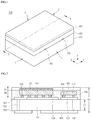
- FIG. 1 is a perspective view showing a light emitting device according to the first example
- FIG. 2 is a side sectional view taken along line A-A of a light emitting device shown in FIG. 1
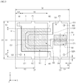
- FIG. 3 is a plan view showing a light emitting chip and a protective chip mounted on a body shown in FIG. 1
- FIG. 4 a plan view showing a body according to the first example
- FIG. 5 is a bottom view of a light emitting device show in FIG. 1
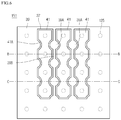
- FIG. 6 is a plan view showing a light emitting chip of FIG. 3
- FIG. 7 is a sectional view taken along line B-B of a light emitting chip shown in FIG. 6
- FIG. 8 is a sectional view taken along line C-C of a light emitting chip shown in FIG. 6 .
- the light emitting device 100 includes a body 101; first and second lead electrodes 121 ad 131 disposed on a top surface of the body 101;, third and fourth electrodes 123 and 133 disposed on the bottom surface of the body 101; at least one first connection electrode 122 and 122A connecting the first and third lead electrodes 121 and 123 to each other through the body 101; a second connection electrode 132 connecting the second and fourth lead electrodes 131 and 133 to each other through the body 101; a light emitting chip 151 disposed on the first and second lead electrodes 121 ad 131; a protective chip 171 formed on the first and second lead electrodes 121 ad 131; a first resin layer 155 disposed around the light emitting chip 151 and the protective chip 151; a second resin layer disposed on the first resin layer 155; and a phosphor layer 153 between the light emitting chip 151 and the second resin layer.
- the body 101 includes an insulating material, for example, a ceramic material.
- the ceramic material may include LTCC (low temperature co-fired ceramic) or HTCC (high temperature co-fired ceramic).
- the body 101 may include metal oxide, such as SiO 2 , Si x O y , Si 3 N 4 , Si x N y , SiO x N y , Al 2 O 3 , or A1N.
- the body 101 may include AlN or Al 2 O 3 , or metal oxide having thermal conductivity of 140W/mK.
- the body 101 may be disposed by using a resin-based insulating material, such as PPA (polyphthalamide).
- the body 101 may be disposed by using silicon, epoxy resin, thermosetting resin including a plastic material, a high heat-resistance material or a high light-resistance material.
- the silicon includes white resin.
- an acid anhydride, an antioxidant, a release agent, a light reflective material, inorganic filler, a hardening catalyst, a light stabilizer, a lubricant, or titanium dioxide may be selectively added to the body 101.
- the body 101 may be disposed by using at least one selected from the group consisting of epoxy resin, modified epoxy resin, silicon resin, modified silicon resin, acryl resin and urethane resin.
- the body 101 can be disposed by using B-stage solid epoxy resin composition, which can be obtained by mixing the epoxy resin, such as triglycidylisocyanurate or hydride bisphenol A diglycidylether, with the acid anhydride promoter, such as hexahydro phthalic anhydride, 3-methyl hexahydro phthalic anhydride or 4-methyl hexahydro phthalic anhydride, and then partially hardening the mixture after adding DBU(1.8-Diazabicyclo(5,4,0)undecene-7) serving as a hardening accelerator and ethylene glycol, titanium oxide pigment or glass fiber serving as a promoter to the epoxy resin, but the example is not limited thereto.
- the epoxy resin such as triglycidylisocyanurate or hydride bisphenol A diglycidylether
- the acid anhydride promoter such as hexahydro phthalic anhydride, 3-methyl hexahydro phthalic anhydride or 4-methyl
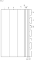
- the body 101 includes first and second sides 1 and 2, which are opposite to each other, and third and fourth sides 3 and 4, which are adjacent to the first and second sides 1 and 2 and opposite to each other.
- the length D1 of the first and second sides 1 and 2 may be longer than the length D2 of the third and fourth sides 3 and 4.
- the length D1 may be in the range of 1.6mm ⁇ 0.5mm
- the length D2 may be in the range of 2.2mm ⁇ 0.5mm, which is at least twice longer than a width A2 of the light emitting chip 151.
- a line C1 extending through the center of the first and second sides 1 and 2 may be aligned with the center of the light emitting chip 151 and the protective chip 171.
- the lengths D1 and D2 may vary depending on the alignment direction of the light emitting chip 151 and the protective chip 171, and the example does not limit the lengths D1 and D2.
- the light emitting chip 151 is disposed adjacent to the first side 1 of the body 101 and the protective chip 171 is disposed adjacent to the second side 2 of the body 101.
- a distance D3 between a center line C2 of the light emitting chip 151 and the first side 1 of the body 101 is in the range of 0.7mm ⁇ 0.1 mm
- a distance D4 between a center line C3 of the protective chip 171 and the second side 2 of the body 101 is in the range of 0.36mm ⁇ 0.05mm.
- the distance D3 may be longer than the distance D4.
- the distance D3 is about twice longer than the distance D4 to allow the light emitting chip 151 to be disposed closer to the center position of the body 101 and to protect the light emitting chip 151.
- the width A1 of the light emitting chip 151 in the first direction may be the same as the width A2 of the light emitting chip 151 in the second direction, but the example is not limited thereto.
- the widths A1 and A2 are in the range of 1mm ⁇ 0.5mm.
- the protective chip 171 may have a width corresponding to 1/2 of the widths A1 and A2 of the light emitting chip 151 in at least one of the first and second directions.
- a thickness T1 of the body 101 is in the range of 380 ⁇ m ⁇ 5 ⁇ m to support the light emitting device.
- first to fourth lead electrodes 121, 131, 123 and 133 are disposed in the body 101.
- the first and second lead electrodes 121 and 131 are disposed on the top surface of the body 101 and the third and fourth lead electrodes 123 and 133 are disposed on the bottom surface of the body 101.
- the first lead electrode 121 includes first and second bonding parts B1 and B2 and the first bonding part B1 is disposed with an open receiving region therein.
- the second bonding part B2 extends from the first bonding part B1.
- the second lead electrode 131 includes third and fourth bonding parts B3 and B4, in which the third bonding part B3 has a protrusion structure and is corresponded to the receiving region of the first bonding part B1 of the first lead electrode 121.
- a gap part 124 is disposed between the first and third bonding parts B1 and B3. At least three sides, for instance, three to seven sides of the first and third bonding parts B1 and B3 may correspond to each other in the gap part 124.
- the first bonding part B1 is disposed around the third bonding part B3 to spread the current through an electrode of the light emitting chip 151.
- the fourth bonding part B4 extends from the third bonding part B3 and is disposed corresponding to the second bonding part B2 of the first lead electrode 121.
- the third bonding part B3 having a width wider than a width of the first bonding part B1 is disposed in the first bonding part B1, so that the bonding area with respect to the electrode can be increased at the center of the light emitting chip 151.
- the current can be effectively spread in the light emitting chip 151.
- the first lead electrode 121 has a plurality of recess parts M1, M2 and M3 around the first bonding part B1.
- the recess parts M1, M2 and M3 are disposed corresponding to at least three edges of the light emitting chip 151.
- the recess parts M1, M2 and M3 are align marks for mounting the light emitting chip 151 and disposed inward than the outer peripheral surface of the first lead electrode 121.
- the recess parts M1, M2 and M3 are disposed in a region where the first lead electrode 121 is partially removed.
- a distance between the first and second recess parts M1 and M2 is the same as the width A2 of the light emitting chip 151 in the second direction. That is, the first and second recess parts M1 and M2 are spaced apart from each other corresponding to the length of one side of the light emitting chip 151.
- a distance between the second and third recess parts M2 and M3 is the same as the width A1 of the light emitting chip 151 in the first direction. That is, the second and third recess parts M2 and M3 are spaced apart from each other corresponding to the length of another one side of the light emitting chip 151. Further, the first and third recess parts M1 and M3 are spaced apart from each other corresponding to the diagonal length of the light emitting chip 151.
- connection electrode 122 having the via structure is disposed at a region adjacent to an edge of the light emitting chip 151 where the recess parts M1, M2 and M3 are not disposed. That is, the connection electrode 122 is spaced apart from the first and third recess parts M1 and M3. For instance, the connection electrode 122 is spaced apart from the first and third recess parts M1 and M3 by the width A2 of the light emitting chip 151, that is, by a distance longer than the length of one side of the light emitting chip 151.
- Depths E1, E2 and E3 of the first to third recess parts M1, M2 and M3 may correspond to the distances between the light emitting chip 151 and sides 1, 3 and 4 of the body 101.
- the depths E2 and E3 of the second and third recess parts M2 and M3 are equal to each other and different from the depth E1 of the first recess part M1.
- the light emitting chip 151 is aligned on the first to third recess parts M1, M2 and M3 and then mounted on the first and third bonding parts B1 and B3 of the first and second lead electrodes 121 and 131.
- First and second support protrusions P1 and P2 are disposed on the first lead electrode 121, in which the first support protrusion P1 is exposed to the third side 3 of the body 101 and the second support protrusion P2 is exposed to the fourth side 4 of the body 101.
- Third and fourth support protrusions P3 and P4 are disposed on the second lead electrode 131, in which the third support protrusion P3 is exposed to the third side 3 of the body 101 and the fourth support protrusion P4 is exposed to the fourth side 4 of the body 101.
- the first and second support protrusions P1 and P2 are disposed adjacent to the line C2 extending through the center of the light emitting chip and first and third bonding parts B1 and B3 are disposed on the line C1.
- the third and fourth support protrusions P3 and P4 can be disposed on the center aligned with the center of the line C3 extending through the center of the protective chip 171.
- Outer surfaces of the first and second lead electrodes 121 and 131 are spaced apart from the sides 1, 2, 3 and 4 of the body 101 by predetermined distances G1 and G2 so that the first and second lead electrodes 121 and 131 can be prevented from being delaminated.
- the distances G1 and G2 have the size of 50 ⁇ m or above, for instance, in the range of 150 ⁇ m to 200 ⁇ m such that a lower portion of the first resin layer can sufficiently make contact with the top surface of the body 101.
- exposure of the first and second lead electrodes 121 and 131 to the outside is diminished to improve the electric reliability.
- the first and third bonding parts B1 and B3 are disposed between the first and second support protrusions P1 and P2 and a segment of a line connecting the first and second support protrusions P1 and P2 to each other may extend through the center of the light emitting chip 151.
- the first and second support protrusions P1 and P2 are disposed in opposition to each other about the first and third bonding parts B1 and B3 to support the region of the first and third bonding parts B1 and B3.
- the second and fourth bonding parts B2 and B4 are disposed between the third and fourth support protrusions P3 and P4 and a segment of a line connecting the third and fourth support protrusions P3 and P4 to each other may extend through the center of the protective chip 171.
- the third and fourth support protrusions P3 and P4 are disposed in opposition to each other about the second and fourth bonding parts B2 and B4 to support the region of the second and fourth bonding parts B2 and B4.
- a virtual line connecting the first and second support protrusions P1 and P2 to each other may be aligned with the center of the light emitting chip 151 and a virtual line connecting the third and fourth support protrusions P3 and P4 to each other may be aligned with the center of the protective chip 171.
- the first to fourth support protrusions P1 to P4 make contact with the lower portion of the first resin layer 155 so that the first to fourth support protrusions P1 to P4 can be prevented from being delaminated from the top surface of the body 101.
- the gap part 124 is disposed between the first and second lead electrodes 121 and 131.
- the gap part 124 may include first gap parts R1 to R5 disposed between the first and third bonding parts B1 and B3, and a second gap part R6 disposed between the second and fourth bonding parts M2 and M4.
- the first gap parts R1 to R5 may include first and second regions R1 and R2, which are spaced apart from each other by a width D8 of the third bonding part B3 in parallel to each other, and a third region R3 connected to the first and second regions R1 and R2 perpendicularly to the first and second regions R1 and R2.
- the first gap parts R1 to R5 may include fourth and fifth regions R4 and R5 which are bent between the third region R3 and the first and second regions R1 and R2.
- the fourth and fifth regions R4 and R5 may be curved or bent at an obtuse angle between the third region R3 and the first and second regions R1 and R2.
- at least one of the fourth and fifth regions R4 and R5 may be omitted and the example is not limited thereto.
- the second gap part R6 includes a sixth region R6 which is parallel to the first and second regions R1 and R2 and vertical to the third region R3.
- the sixth region R6 is spaced apart from the second region R2 by a predetermined distance and connected to the second region R2.
- the center of the sixth region R6 is aligned with the center between the first and second regions R1 and R2.
- the third and fourth lead electrodes 123 and 133 are disposed on a bottom surface 102 of the body 101.
- the third lead electrode 123 is connected to the first lead electrode 121 through the first connection electrodes 122 and 122A and the fourth lead electrode 133 is connected to the second lead electrode 131 through the second connection electrode 132.
- At least one of the first connection electrodes 122 and 122A is disposed in the body 101 and connected to the first and third lead electrodes 121 and 123.
- At least one second connection electrode 132 is disposed in the body 101 and connected to the second and fourth electrodes 131 and 133.
- An area of the bottom surface of the third lead electrode 123 is different from an area of the bottom surface of the fourth lead electrode 133.
- the area of the bottom surface of the third lead electrode 123 is larger than the area of the bottom surface of the fourth lead electrode 133.
- the first to fourth lead electrodes 121, 131, 123 and 133 may include a plurality of metals selected from the group consisting of Ti, Cu, Ni, Au, Cr, Ta, Pt, Pd, Sn, Ag, and P and may be prepared as a multi-layer structure.
- the first to fourth lead electrodes 121, 131, 123 and 133 may have a stack structure of Cu/Ni/Pd/Au. Since an Au-coating layer is disposed on the surface of the first to fourth lead electrodes 121, 131, 123 and 133, corrosion caused by penetration of moisture can be suppressed and the electric reliability can be improved.
- the first to fourth lead electrodes 121, 131, 123 and 133 may have a thickness in the range of 80 ⁇ 2 ⁇ m.
- Cu has a thickness in the range of 7.5 ⁇ 1.5 ⁇ m
- Ni has a thickness in the range of 5 ⁇ 1.5 ⁇ m
- Pd or Au has as a thickness in the range of 0.1 ⁇ 0.3 ⁇ m. Since Cu has the thick thickness, the heat conductive efficiency can be improved.
- the coating layer is disposed except for outer surfaces of the first to fourth support protrusions P1 to P4. Since the first to fourth support protrusions P1 to P4 are present in the cutting surface, the coating layer is removed from the outer surfaces of the first to fourth support protrusions P1 to P4.
- the coating layer is disposed on the surfaces of the third and fourth lead electrodes 123 and 133.
- the light emitting chip 151 is disposed on the first and second lead electrodes 121 and 131 disposed on the center region of the body 101, and the protective chip 171 is disposed on the first and second lead electrodes 121 and 131 disposed on the side region of the body 101.
- the light emitting chip 151 is a light source capable of selectively emitting lights having the wavelength bands ranging from the ultraviolet ray band to the visible ray band.
- the light emitting chip 151 may include a UV (ultraviolet) LED (light emitting diode) chip, a green LED chip, a blue LED chip, and a red LED chip.
- a phosphor may be coated on a light emission region of the light emitting chip 151, but the example is not limited thereto.
- the light emitting chip 151 is bonded to the first and second lead electrodes 121 and 131 by a plurality of first bonding members 125, and the protective chip 171 is bonded onto the first and second lead electrodes 121 and 131 by a plurality of second bonding members 127.
- the first and second bonding members 125 and 126 may be disposed by using conductive materials, such as solder materials.
- the light emitting chip 151 may have a thickness of 100 ⁇ m or above and the protective chip 171 may have a thickness in the range of 90 ⁇ m to 105 ⁇ m.
- the protective chip 171 may be implemented in the form of a thyristor, a zener diode or TVS (transient voltage suppression) and the protective chip 171 protects the light emitting chip 151 from ESD (electrostatic discharge).
- the phosphor layer 153 has a thickness D7 in the range of 0.15 ⁇ m to 60 ⁇ m.
- the light emitting device has a thickness D5 in the range of 0.75mm ⁇ 0.05mm. The above thicknesses are determined by taking the support for the light emitting chip 151 and the thermal conductive efficiency into consideration.
- the first resin layer 155 is disposed around the light emitting chip 151 without covering the top surface of the light emitting chip 151.
- the first resin layer 155 is positioned higher than the periphery and the top surface of the protective chip 171 to cover the top surface of the protective chip 171.
- a part of the first resin layer 155 is disposed among the top surfaces of the first and second lead electrodes 121 and 131, the light emitting chip 151 and the protective chip 171.
- Metal oxide is added to a resin material of the first resin layer 155.
- the resin material includes silicon or epoxy and the metal oxide has a refractive index higher than that of the resin material.
- the metal oxide may include TiO 2 or SiO 2 .
- At least 5wt% or more of the metal oxide is added to the first resin layer 155.
- 5wt% to 15wt% of the metal oxide is added to the first resin layer 155.
- the first resin layer 155 having the metal oxide may serve as a reflective member around the light emitting chip 151.
- the reflective member represents reflectivity of at least 50% or more, for instance, 78% with respect to the light emitted from the light emitting chip 151.
- the metal oxide contained in the first resin layer 155 exceeds 15wt%, viscosity of the first resin layer 155 may be remarkably lowered, so the moisture may penetrate into the first resin layer 155 and bonding strength of the first resin layer 155 with respect to other materials may be lowered.
- the content of the metal oxide in the first resin layer 155 is lowered, the reflective efficiency may be lowered, causing degradation of the light extraction efficiency.
- the phosphor layer 153 is disposed on the light emitting chip 151.
- the phosphor layer 153 absorbs a part of the light emitted from the light emitting chip 151 to convert the wavelength of the light.
- the phosphor layer 153 may be disposed by adding a phosphor to a transmissive resin material, such as silicon or epoxy.
- the phosphor may include at least one of a yellow phosphor, a green phosphor, a blue phosphor and a red phosphor.
- the phosphor may include at least one selected from the group consisting of a nitride based phosphor, an oxy-nitride based phosphor and a sialon based phosphor, which are mainly activated by lanthanoid based elements, such as Eu or Ce; an alkali earth halogen apatite phosphor, which is mainly activated by a lanthanoid based element, such as Eu, or a transient metallic element, such as Mn; an alkali earth metal boric acid halogen phosphor; an alkali earth metal aluminate phosphor; an alkali earth silicate; an alkali earth sulfide; an alkali earth thio-gallate; an alkali earth silicon nitride; a germinate; a rare-earth aluminate mainly activated by a lanthanoid based element, such as Ce; a rare-earth silicate; and an organic chel
- a second resin layer 161 is disposed on the first resin layer 155 and the phosphor layer 153.
- the second resin layer 161 is a clean molding material to which additives, such as a phosphor, a diffusing agent or a scattering agent, may not be added, that is, impurities having the refractive index higher than that of the resin material may not be added.
- the second resin layer 161 may serve as a light exit surface and a top surface of the second resin layer 161 may be concave or convex.
- the second resin layer 161 may have a thickness thicker than that of the phosphor layer 153, but the example is not limited thereto.
- FIG. 6 is a plan view showing the light emitting chip of FIG. 2
- FIG. 7 is a sectional view taken along line B-B of the light emitting chip shown in FIG. 6
- FIG. 8 is a sectional view taken along line C-C of the light emitting chip shown in FIG. 6 .
- the light emitting chip 151 includes a plurality of second electrodes 41 provided inside the light emitting chip 151 without being exposed to the lateral side of the light emitting chip 151, and a first electrode 39 disposed around the second electrodes 41.
- the second electrodes 41 are disposed inside the first electrode 39 and mounted on the third bonding part B3 of the second lead electrode 123.
- the second electrodes 41 may be regularly aligned.
- Each of the second electrodes 41 includes a plurality of concave parts 41A having the structure corresponding to convex parts of the first electrode 39.
- a part of the first electrode 39 may be disposed among the second electrodes 41.
- the first electrode 39 may have a connection structure through the regions among the second electrodes 41.
- the first electrode 39 is disposed over the entire area of the light emitting chip 151 and includes bridge electrodes 39B disposed among the second electrodes 41 and contact parts 39A connected to the bridge electrodes 39B and disposed on the concave parts 41A of the second electrodes 41.
- the concave part 41A of the second electrode 41 may have a hemispherical shape, but the example is not limited thereto.
- the first electrode 39 is connected to the first lead electrode 121 and the second electrodes 41 are connected to the second lead electrode 131 by the first bonding member 125.
- the bridge electrode 39B may have a top surface lower than top surfaces of the first and second electrodes 39 and 41, but the example is not limited thereto.
- the light emitting chip 151 may include a substrate 11, a buffer layer 13, a low-conductive layer 15, a first conductive semiconductor layer 21, an active layer 23, a second conductive semiconductor layer 25, a first electrode layer 31, a reflective layer 33, an insulating layer 37, the first electrode 39 and the second electrodes 41.
- the substrate 11 may include a transmissive substrate, an insulating substrate or a conductive substrate.
- the substrate 11 may include at least one of Al 2 O 3 , SiC, Si, GaAs, GaN, ZnO, Si, GaP, InP, Ge, Ga 2 O 3 and LiGaO 3 .
- a plurality of protrusions may be disposed on at least one of a top surface and a bottom surface of the substrate 11.
- the protrusions can be disposed in a shape of a stripe, a hemisphere or a dome by etching the substrate 11 or can be disposed as a separate light extracting structure, such as a roughness.
- the substrate 11 may have a thickness in the range of 30 ⁇ m to 300 ⁇ m.
- the substrate 11 can be removed from the light emitting chip 151. In this case, the phosphor layer directly makes contact with the first conductive semiconductor layer.
- a plurality of compound semiconductor layers may be grown on the substrate 11.
- the compound semiconductor layers may be disposed through an E-beam evaporator, PVD (physical vapor deposition), CVD (chemical vapor deposition), PLD (plasma laser deposition), a dual-type thermal evaporator, sputtering, or MOCVD (metal organic chemical vapor deposition), but the example is not limited thereto.
- the buffer layer 13 may be disposed on the substrate 11.
- the buffer layer 13 may be prepared as at least one layer by using a group II-VI or a group III to V compound semiconductor.
- the buffer layer 13 may include a semiconductor layer disposed by using the group III-V compound semiconductor.
- the buffer layer 13 may include at least one of compound semiconductors having the compositional formula of In x Al y Ga 1-x-y N (0 ⁇ x ⁇ 1, 0 ⁇ y ⁇ 1, 0 ⁇ x+y ⁇ 1), such as GaN, InN, A1N, InGaN, AlGaN, InAlGaN, and AlInN.
- the buffer layer 13 may have the superlattice structure by alternately stacking heterogeneous semiconductor layers.
- the buffer layer 13 may attenuate the lattice mismatch between the substrate 11 and the nitride semiconductor layer and may be defined as a defect control layer.
- the buffer layer 13 may have a lattice constant between a lattice constant of the substrate 11 and a lattice constant of the nitride semiconductor layer.
- the buffer layer 13 may be disposed by using oxide, such as ZnO, but the example is not limited thereto.
- the buffer layer 13 may have a thickness in the range of 30nm to 500nm, but the example is not limited thereto.
- the low-conductive layer 15 is disposed on the buffer layer 13.
- the low-conductive layer 15 includes an undoped semiconductor layer having conductivity lower than that of the first conductive semiconductor layer 21.
- the low-conductive layer 15 can be disposed by using the group III-V compound semiconductor, for instance, a GaN-based semiconductor.
- the undoped semiconductor layer has a low conductive property even if a conductive dopant is not intentionally doped thereto.
- At least one or all of the buffer layer 13 and the low-conductive layer 15 may be omitted from the light emitting chip 151, and the example is not limited thereto.
- the first conductive semiconductor layer 21 is disposed on the low-conductive layer 15.
- the first conductive semiconductor layer 21 can be disposed by using the group III-V compound semiconductor doped with a first conductive dopant.
- the first conductive semiconductor layer 21 can be disposed by using a semiconductor material having the compositional formula of In x Al y Ga 1-x-y N (0 ⁇ x ⁇ 1, 0 ⁇ y ⁇ 1, 0 ⁇ x+y ⁇ 1).
- the first conductive semiconductor layer 21 may be an n type semiconductor layer. If the first conductive semiconductor layer 21 is the n type semiconductor layer, the first conductive dopant includes the n type dopant, such as Si, Ge, Sn, Se or Te.
- At least one of the low-conductive layer 15 and the first conductive semiconductor layer 21 may have the superlattice structure, in which heterogeneous first and second semiconductor layers are alternately stacked.
- Each of the first and second layers may have a thickness of about several ⁇ or above.
- a first clad layer (not shown) may be disposed between the first conductive semiconductor layer 21 and the active layer 23.
- the first clad layer may include a GaN-based semiconductor and may confine the carriers.
- the first clad layer may have the superlattice structure of InGaN or InGaN/GaN, but the example is not limited thereto.
- the first clad layer may include n type and/or p type dopant.
- the first clad layer may be prepared as a first conductive semiconductor layer or a low-conductive semiconductor layer.
- the active layer 23 is disposed on the first conductive semiconductor layer 21 or the first clad layer.
- the active layer 23 may include at least one of a single quantum well structure, a multiple quantum well (MQW) structure, a quantum dot structure, and a quantum wire structure.
- the active layer 23 may have a stack structure of well/barrier layers.
- the well layer may have a continuous energy level.
- the well layer may be a quantum well layer having the quantum energy level.
- the well layer may be defined as a quantum well layer and the barrier layer may be defined as a quantum barrier layer.
- the well/barrier layers may repeat with the periodicity of 2 to 30.
- the well layer can be disposed by using a semiconductor material having the compositional formula of In x Al y Ga 1-x-y N (0 ⁇ x ⁇ 1, 0 ⁇ y ⁇ 1, 0 ⁇ x+y ⁇ 1).
- the barrier layer may be prepared as a semiconductor layer having a bandgap wider than that of the well layer.
- the barrier layer can be disposed by using a semiconductor material having the compositional formula of In x AlyGa 1-x-y N (0 ⁇ x ⁇ 1, 0 ⁇ y ⁇ 1, 0 ⁇ x+y ⁇ 1).
- the stack structure of the well/barrier layers may include at least one of InGaN/GaN, AlGaN/GaN, InGaN/AlGaN, and InGaN/InGaN.
- the well layer may have the thickness in the range of 1.5nm to 5nm, for instance, 2nm to 4nm.
- the barrier layer has the thickness in the range of 5nm to 30nm, for instance, 5nm to 7nm, which is thicker than that of the well layer.
- the n type dopant may be doped into the barrier layer, but the example is not limited thereto.
- the active layer 23 may selectively emit the light having the wavelength bands ranging from the ultraviolet ray band to the visible ray band. For instance, the active layer 23 may emit the light having the peak wavelength in the range of 420nm to 450nm.
- a second clad layer (not shown) may be disposed on the active layer 23.
- the bandgap of the second clad layer is wider than the bandgap of the barrier layer of the active layer 23.
- the second conductive clad layer may include the group III-V compound semiconductor, such as a GaN-based semiconductor.
- the second clad layer may have the superlattice structure of GaN, AlGaN or InAlGaN.
- the second clad layer may include the n type and/or p type dopants and may be prepared as a second conductive semiconductor layer or a low-conductive semiconductor layer.
- the second conductive semiconductor layer 25 is disposed on the second clad layer (not shown) or the active layer 23.
- the second conductive semiconductor layer 25 may include a second conductive dopant.
- the second conductive semiconductor layer 25 may include at least one of compound semiconductors, such as GaN, InN, A1N, InGaN, AlGaN, InAlGaN, and AlInN. If the second conductive semiconductor layer 25 is a p type semiconductor layer, the second conductive dopant is a p type dopant, such as Mg, Zn, Ca, Sr or Ba.
- the first conductive semiconductor layer 21, the active layer 23 and the second conductive semiconductor layer 25 may constitute a light emitting structure layer 20.
- the conductive types of the first and second conductive semiconductor layers 21 and 25 may be changed inversely to the above.
- the second conductive semiconductor layer 25 may be prepared as the n type semiconductor layer and the first conductive semiconductor layer 21 may be prepared as the p type semiconductor layer.
- an n type semiconductor layer which is a third conductive semiconductor layer having polarity opposite to that of the second conductive semiconductor layer 25, can be disposed on the second conductive semiconductor layer 25.
- the light emitting structure layer 20 may have one of an n-p junction structure, a p-n junction structure, an n-p-n junction structure, and a p-n-p junction structure.
- the active layer 23 is disposed between two layers.
- at least one active layer 23 is disposed among three layers.
- the first electrode layer 31, the reflective layer 33, the second electrode layer 35, the insulating layer 37 and the second electrodes 41 are disposed on the light emitting structure layer 20 and the first electrode 39 is disposed on a part of the light emitting structure layer 20.
- the first electrode layer 31 is a current spreading layer and includes transmissive and electric conductive materials.
- the first electrode layer 31 may be prepared as a transparent electrode layer having a refractive index lower than that of the compound semiconductor layer.
- the first electrode layer 31 is disposed on the top surface of the second conductive semiconductor layer 25 and includes at least one of metal oxide and metal nitride.
- the first electrode layer 31 may include one selected from the group consisting of ITO (indium tin oxide), IZO (indium zinc oxide), IZTO (indium zinc tin oxide), IAZO (indium aluminum zinc oxide), IGZO (indium gallium zinc oxide), IGTO (indium gallium tin oxide), AZO (aluminum zinc oxide), ATO (antimony tin oxide), GZO (gallium zinc oxide), ZnO, IrOx, RuOx and NiO.
- the first electrode layer 31 may be prepared as at least one layer.
- the first electrode layer 31 can be shallowly disposed by using at least one selected from the group consisting of Al, Ag, Pd, Rh, Pt Ir and an alloy thereof in such a manner that the light can pass through the first electrode layer 31.
- the first electrode layer 31 may have a thickness of 5.0 nm or less, for example, 1.0 nm.
- the reflective layer 33 is disposed on the first electrode layer 31.
- the reflective layer 33 may include Ag or Al.
- A1 is used for the reflective layer 33 because A1 represents reflectivity higher than that of Ag.
- An adhesive layer (not shown) may be partially disposed on a region between the first electrode layer 31 and the reflective layer 33.
- the adhesive layer may include a fluoric transient metal compound representing the transmittance of 80% or more with respect to the light having the wavelength of 450nm. Since the adhesive layer represents higher adhesive force with respect to the A1 reflective layer, rather than the Ag reflective layer, the adhesive property of the reflective layer 33 can be improved. Since the adhesive property of the reflective layer 33 is improved, the reflective efficiency can also be improved.
- the adhesive layer may have a thickness in the range of 10nm to 1 ⁇ m by taking the adhesive strength with respect to the reflective layer 33 into consideration.
- the second electrode layer 35 is disposed on the reflective layer 33.
- the second electrode layer 35 may be disposed by using a metal layer, such as a barrier metal layer.
- the second electrode layer 35 may include at least one of Ti, W, Ru, Rh, Ir, Mg, Zn, Al, In, Ta, Pd, Co, Ni, Si, Ge, Ag and Au and can be prepared as a single layer or a multi-layer.
- the second electrode layer 35 may be disposed by using an alloy, such as TiW (Titanium Tungsten), but the example is not limited thereto.
- the first electrode layer 31, the reflective layer 33 and the second electrode layer 35 may have the stack structure of ITO/Ag/TiW.
- the first electrode layer 31 may be omitted.
- At least one recess 19 is disposed in the light emitting structure layer 20 and the at least one recess 19 may have a depth sufficient for exposing the light emitting structure layer 20 from the second conductive semiconductor layer 25 to a part of the first conductive semiconductor layer 21.
- a plurality of recesses 19 can be provided while being spaced apart from each other, but the example is not limited thereto.
- the insulating layer 37 is disposed on the second electrode layer 35 and extends around the recess 19.
- a hole is disposed in the insulating layer 37 disposed in the recess 19 and a part 39A of the first electrode 39 is disposed in the hole.
- the part 39A of the first electrode 39 has the via structure and physical makes contact with the first conductive semiconductor layer 21.
- the insulating layer 37 may also be disposed at the sidewall between the first electrode 39 and the light emitting structure layer 20.
- the insulating layer 37 may include an insulating material or an insulating resin, such as oxide, nitride, fluoride or sulfide of Al, Cr, Si, Ti, Zn or Zr.
- the insulating layer 37 may include one elected from the group consisting of SiO 2 , Si 3 N 4 , Al 2 O 3 , and TiO 2 .
- the insulating layer 37 can be prepared as a single layer or a multi-layer, and the example is not limited thereto.
- the insulating layer 37 may include a non-conductive metal compound, such as a fluoride metal compound.
- a fluoride metal compound such as a fluoride metal compound.
- the insulating layer 37 may be prepared as MxFy, in which M includes at least one of metals, such as Ga, Mg and Al, and a transient metal, x is in the range of 1 to 3, and y is 2 or 3.
- the fluoride transient metal compound includes MgF 2 , AlF 3 , or GaF 3 .
- the first electrode layer 31 is disposed on the light emitting structure layer 20, the reflective layer 33 is disposed on the first electrode layer 31, and the second electrode layer 35 is disposed on the reflective layer 33.
- the reflective layer 33 can cover about 80% or more of the top portion of the light emitting structure 20 and the adhesive strength of the reflective layer 33 can be improved by the adhesive layer.
- the second electrode layer 35 can make contact with the lateral sides of the first electrode layer 31 and the reflective layer 33, and the example is not limited thereto.
- the second electrodes 41 are disposed on the second electrode layer 35.
- the second electrodes 41 may branch in the form of an arm pattern and are connected with each other.
- a part of the insulating layer 37 may be further disposed between the second electrode 41 and the second electrode layer 35, but the example is not limited thereto.
- the first electrode 39 may have an upper width wider than a lower width thereof and the second electrode 41 may have an upper width wider than a lower width thereof
- the first and second electrodes 39 and 41 can be mounted on the substrate or in the package in a flip scheme.
- the first and second electrodes 39 and 41 may include Cr, Ti, Co, Ni, V, Hf, Ag, Al, Ru, Rh, Pt, Pd, Ni, Mo, W, La, Ta, Ti or an alloy thereof and can be prepared as a single layer or a multi-layer.
- the first and second electrodes 39 and 41 may have the same metal stack structure.
- the first and second electrodes 39 and 41 may have the stack structure of Cr/NiAl/Au, but the example is not limited thereto.
- the light emitting chip 151 a part of the light emitted from the active layer 23 is reflected from the reflective layer 33 and extracted toward the substrate 11 and the sidewall.
- the light emitting chip 151 can be bonded onto the substrate or in the package in a flip scheme.
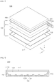
- FIG. 9 is a side sectional view showing a light emitting device according to the second example.
- the description about the first example will be incorporated by reference.
- the light emitting device includes a body 101, a plurality of lead electrodes 121, 131, 123 and 133, a plurality of connection electrodes 122 and 132, a light emitting chip 151, a protective chip 171, a first resin layer 155, a second resin layer 151 and a phosphor layer 154.
- the phosphor layer 154 extends from the top surface to the lateral side of the light emitting chip 151. Since the phosphor layer 154 is disposed on the top surface and the lateral side of the light emitting chip 151, a part of the light emitted from the active layer of the light emitting chip 151 is converted to have a long wavelength by a phosphor of the phosphor layer 154.
- the phosphor layer 154 disposed on the lateral side of the light emitting chip 151 makes contact with the first resin layer 155 so that the adhesive property of the phosphor layer 154 can be improved and the light loss caused by the light reflection at the first resin layer 155 can be prevented.
- the second resin layer 155 is disposed around the light emitting chip 151 and makes contact with all lateral sides of the light emitting chip 151.
- the first resin layer 155 can be disposed by adding first metal oxide to a silicon material.
- the first metal oxide includes a material having a high refractive index, such as TiO 2 having a refractive index of 2.0 or more.
- the content of the first metal oxide added to the first resin layer 155 is in the range of 5 wt% to 15wt%, for instance, 10 wt% to 15 wt%.
- the silicon material of the first resin layer 155 has the refractive index in the range of 1.51 to 1.55. Such a silicon material has the superior adhesive property with respect to other materials.
- the first resin layer 155 including the first metal oxide may serve as a reflective layer capable of reflecting about 70% or more of the light emitted from the light emitting chip 151. Since the first resin layer 155 serves as the reflective layer, the light emitted in the lateral direction of the light emitting chip 151 can be effectively reflected.
- a first molding member 155 is bonded to the lateral side of the light emitting chip 151 so the beam distribution of the light emitted from the light emitting chip 151 can be improved.
- the second resin layer 161 may be disposed by using a material having superior adhesive property with respect to the first resin layer 155.
- the second resin layer 161 may include a material the same as a material of the first resin layer 155.
- the second resin layer 161 makes contact with the top surfaces of the first resin layer 155 and the light emitting chip 151.
- the second resin layer 161 can be disposed by adding second metal oxide to a silicon material.
- the second metal oxide includes a material having a high refractive index and is different from the first metal oxide added to the first resin layer 155.
- the second metal oxide may include SiO 2 having a refractive index of 2 or less.
- the second resin layer 161, which is disposed by adding the second metal oxide to the silicon material may serve as a diffusion layer. If the first and second resin layers 155 and 161 are disposed by using the same material, a bubble and an interfacial de-adhesion can be prevented at the interfacial surface between the first and second resin layers 155 and 161.
- FIG. 10 is a side sectional view showing a light emitting device according to an embodiment In the following description of the embodiment, the description about the first example will be incorporated by reference.
- the light emitting device includes a body 101, a plurality of lead electrodes 121, 131, 123 and 133, a plurality of connection electrodes 122 and 132, a light emitting chip 151, a protective chip 171, a first resin layer 155, a second resin layer 161 and a phosphor layer 153.
- the first resin layer 155 has a recess 155A having a bottom surface higher than a bottom surface of the light emitting chip 51.
- the bottom surface of the recess 155A may have the height similar to or equal to a top surface line L1 of a reflective layer in the light emitting chip 151.
- an inner wall of the recess 155A is inclined with respect to the lateral side of the light emitting chip 151 or the bottom surface of the recess 155A to reflect the incident light toward the light exit surface.
- a part 161A of the second resin layer 161 which is in contact with an outer peripheral portion of the light emitting chip 151, makes contact with the recess 155A.
- the part 161A of the second resin layer 161 may guide the light emitted from the light emitting chip 151 in the lateral direction.
- the phosphor layer 153 is disposed on the light emitting chip 151 and the top surface of the phosphor layer 153 may be aligned on the same plane with the top surface of the second resin layer 161.
- the phosphor layer 153 may extend to the lateral side of the light emitting chip 151, and the embodiment is not limited thereto. Since the light emitting chip 151 is mounted in a flip scheme, most of the light emitted from the light emitting chip 151 is directed upward and about 20% or less of the light is directed in the lateral direction. Thus, even if the phosphor layer 153 is disposed at the lateral side of the light emitting chip 151, the wavelength conversion rate of the light at the lateral side of the light emitting chip 151 may be low.
- FIG. 11 is a side sectional view showing a light emitting device according to the third example.
- the description about the first example will be incorporated by reference.
- the light emitting device includes a body 101, a plurality of lead electrodes 121, 131, 123 and 133, a plurality of connection electrodes 122 and 132, a light emitting chip 151, a protective chip 171, a first resin layer 156, a second resin layer 162, a third resin layer 157 and a phosphor layer 163.
- the top surface of the first resin layer 156 is aligned corresponding to the line L2 disposed between the bottom surface of the active layer of the light emitting chip 151 and the bottom surface of the second conductive semiconductor layer.
- the top surface of the first resin layer 156 may be lower than the top surface of the protective chip 171 and the light absorbing loss may occur when the protective chip 171 is exposed.
- the third resin layer 157 is disposed on the protective chip 171.
- the third resin layer 157 is disposed on the protective chip 171 and the first resin layer 156 and the metal oxide added to the first resin layer 156 is added to the third resin layer 157 so that the third resin layer 157 may serve as a reflective member.
- About 5wt% or more of the metal oxide may be added to the third resin layer 157.
- the content of the metal oxide added to the third resin layer 157 may be higher than the content of the metal oxide added to the first resin layer 156 in a predetermined ratio (for instance, 5wt% or more).
- the third resin layer 157 is spaced apart from the lateral side of the light emitting chip 151, so the third resin layer 157 may serve as a reflective sidewall.
- the second resin layer 162 is disposed on the light emitting chip 151, the first resin layer 156 and the third resin layer 157. A part of the second resin layer 162 is disposed between the light emitting chip 151 and the third resin layer 157 to induce the light extraction in the lateral direction.
- the phosphor layer 163 is disposed on the second resin layer 162 and on the entire top surface of the light emitting device.
- the phosphor layer 163 can be prepared in the form of a film or a resin layer, but the example is not limited thereto.
- the light emitting device is applicable to a lighting system.
- the lighting system includes a structure in which a plurality of light emitting devices are arrayed.
- the lighting system includes a display apparatus shown in FIGS. 12 and 13 , a lighting apparatus shown in FIG. 14 , a lighting lamp, a camera flash, a signal lamp, a headlamp for a vehicle, and an electronic display.
- FIG. 12 is an exploded perspective view showing a display apparatus having the light emitting device according to the embodiment.
- a display apparatus 1000 includes a light guide plate 1041, a light source module 1031 to supply light to the light guide plate 1041, a reflective member 1022 under the light guide plate 1041, an optical sheet 1051 on the light guide plate 1041, a display panel 1061 on the optical sheet 1051, and a bottom cover 1011 to receive the light guide plate 1041, the light source module 1031, and the reflective member 1022, but the embodiment is not limited thereto.
- the bottom cover 1011, the reflective sheet 1022, the light guide plate 1041, the optical sheet 1051, and the light unit 1050 may be defined as a light unit 1050.
- the light guide plate 1041 diffuses the light supplied from the light source module 1031 to provide surface light.
- the light guide plate 1041 may include a transparent material.
- the light guide plate 1041 may include one of acryl-based resin, such as PMMA (polymethyl methacrylate, PET (polyethylene terephthalate), PC (polycarbonate), COC (cyclic olefin copolymer) and PEN (polyethylene naphtha late) resin.
- PMMA polymethyl methacrylate
- PET polyethylene terephthalate
- PC polycarbonate
- COC cyclic olefin copolymer
- PEN polyethylene naphtha late
- the light source module 1031 is disposed on at least one side of the light guide plate 1041 to supply the light to at least one side of the light guide plate 1041.
- the light source module 1031 serves as the light source of the display device.
- At least one light source module 1031 is disposed to directly or indirectly supply the light from one side of the light guide plate 1041.
- the light source module 1031 may include a substrate 1033 and the light emitting device according to the embodiments or the light emitting device 1035.
- the light emitting device or the light emitting device 1035 are arranged on the substrate 1033 while being spaced apart from each other at the predetermined interval.
- the substrate 1033 may include a printed circuit board (PCB) including a circuit pattern (not shown).
- the substrate 1033 may also include a metal core PCB (MCPCB) or a flexible PCB (FPCB) as well as a typical PCB, but the embodiment is not limited thereto. If the light emitting device 1035 is installed on the side of the bottom cover 1011 or on a heat dissipation plate, the substrate 1033 may be omitted. The heat dissipation plate partially makes contact with the top surface of the bottom cover 1011.
- the light emitting device 1035 are arranged such that light exit surfaces to discharge light of the light emitting device 1035 are spaced apart from the light guide plate 1041 by a predetermined distance on the substrate 1033, but the embodiment is not limited thereto.
- the light emitting device 1035 may directly or indirectly supply the light to a light incident surface, which is one side of the light guide plate 1041, but the embodiment is not limited thereto.
- the reflective member 1022 is disposed under the light guide plate 1041.
- the reflective member 1022 reflects the light, which is traveled downward through the bottom surface of the light guide plate 1041, toward the display panel 1061, thereby improving the brightness of the light unit 1050.
- the reflective member 1022 may include PET, PC or PVC resin, but the embodiment is not limited thereto.
- the reflective member 1022 may serve as the top surface of the bottom cover 1011, but the embodiment is not limited thereto.
- the bottom cover 1011 may receive the light guide plate 1041, the light source module 1031, and the reflective member 1022 therein. To this end, the bottom cover 1011 has a receiving section 1012 having a box shape with an opened top surface, but the embodiment is not limited thereto. The bottom cover 1011 can be coupled with the top cover (not shown), but the embodiment is not limited thereto.
- the bottom cover 1011 can be manufactured through a press process or an extrusion process by using metallic material or resin material.
- the bottom cover 1011 may include metal or non-metallic material having superior thermal conductivity, but the embodiment is not limited thereto.
- the display panel 1061 for example, is an LCD panel including first and second transparent substrates, which are opposite to each other, and a liquid crystal layer interposed between the first and second substrates.
- a polarizing plate can be attached to at least one surface of the display panel 1061, but the embodiment is not limited thereto.
- the display panel 1061 displays information by allowing the light to pass therethrough.
- the display device 1000 can be applied to various portable terminals, monitors of notebook computers, monitors or laptop computers, and televisions.
- the optical sheet 1051 is disposed between the display panel 1061 and the light guide plate 1041 and includes at least one transmissive sheet.
- the optical sheet 1051 includes at least one selected from the group consisting of a diffusion sheet, a horizontal and vertical prism sheet, and a brightness enhanced sheet.
- the diffusion sheet diffuses the incident light
- the horizontal and vertical prism sheet concentrates the incident light onto the display panel 1061
- the brightness enhanced sheet improves the brightness by reusing the lost light.
- a protective sheet can be disposed on the display panel 1061, but the embodiment is not limited thereto.
- the light guide plate 1041 and the optical sheet 1051 can be disposed in the light path of the light source module 1031 as optical members, but the embodiment is not limited thereto.
- FIG. 13 is a sectional view showing a display apparatus according to the embodiment.
- the display apparatus 1100 includes a bottom cover 1152, a substrate 1120 on which the light emitting device 1124 are arrayed, an optical member 1154, and a display panel 1155.
- the substrate 1120 and the light emitting device 1124 may constitute the light source module 1160.
- the bottom cover 1152, at least one light source module 1160, and the optical member 1154 may constitute the light unit.
- the bottom cover 1151 can be disposed with a receiving section 1153, but the embodiment is not limited thereto.
- the light source module 1160 includes a substrate 1120, and a plurality of light emitting devices arranged on the substrate 1120 or a light emitting device 1124.
- the optical member 1154 may include at least one selected from the group consisting of a lens, a light guide plate, a diffusion sheet, a horizontal and vertical prism sheet, and a brightness enhanced sheet.
- the light guide plate may include PC or PMMA (Poly methyl methacrylate). The light guide plate can be omitted.
- the diffusion sheet diffuses the incident light
- the horizontal and vertical prism sheet concentrates the incident light onto a display region
- the brightness enhanced sheet improves the brightness by reusing the lost light.
- the optical member 1154 is disposed above the light source module 1160 in order to convert the light emitted from the light source module 1160 into the surface light.
- FIG. 14 is an exploded perspective view showing a lighting device having the light emitting device according to the embodiment.
- the lighting device may include a cover 2100, a light source module 2200, a heat radiation member 2400, a power supply part 2600, an inner case 2700, and a socket 2800.
- the light emitting device may further include at least one of a member 2300 and a holder 2500.
- the light source module 2200 may include the light emitting device according to the embodiment.
- the cover 2100 has the shape of a bulb, or a hemispherical shape.
- the cover 2100 may have a hollow structure, and a portion of the cover 2100 may be open.
- the cover 2100 may be optically connected to the light source module 2200, and may be coupled with the heat radiation member 2400.
- the cover 2100 may have a recess part coupled with the heat radiation member 2400.
- the inner surface of the cover 2100 may be coated with ivory white pigments serving as a diffusing agent.
- the light emitted from the light source module 2200 may be scattered or diffused by using the ivory white material, so that the light can be discharged to the outside.
- the cover 2100 may include glass, plastic, PP, PE, or PC.
- the PC represents superior light resistance, superior heat resistance, and superior strength.
- the cover 2100 may be transparent so that the light source module 2200 may be recognized at the outside.
- the cover 2100 may be opaque.
- the cover 2100 may be disposed through a blow molding scheme.
- the light source module 2200 may be disposed at one surface of the heat radiation member 2400. Accordingly, the heat emitted from the light source module 2200 is conducted to the heat radiation member 2400.
- the light source module 2200 may include a light emitting device 2210, a connection plate 2230, and a connector 2250.
- the member 2300 is disposed on the top surface of the heat radiation member 2400, and has a guide groove 2310 having a plurality of light emitting devices 2210 and a connector 2250 inserted into the guide groove 2310.
- the guide groove 2310 corresponds to the substrate of the light emitting device 2210 and the connector 2250.
- White pigments may be applied to or coated on the surface of the member 2300.
- the member 2300 reflects light, which reflected by the inner surface of the cover 2100 to return to the light source module 2200, toward the cover 2100. Accordingly, the light efficiency of the lighting apparatus according to the embodiment can be improved.
- the member 2300 may include an insulating material.
- the connection plate 2230 of the light source module 2200 may include an electric-conductive material. Accordingly, the heat radiation member 2400 may be electrically connected to the connection plate 2230.
- the member 2300 includes an insulating material to prevent the electrical short between the connection plate 2230 and the heat radiation member 2400.
- the heat radiation member 2400 receives heat from the light source module 2200 and the heat from the power supply part 2600 and radiates the heats.
- the holder 2500 blocks a receiving groove 2719 of an insulating part 2710 disposed in an internal case 2700. Accordingly, the power supply part 2600 received in the insulating part 2710 of the internal case 2700 is sealed.
- the holder 2500 has a guide protrusion part 2510.
- the guide protrusion part 2510 may include a hole allowing a protrusion part 2610 of the power supply part 2600 to pass therethrough.
- the power supply part 2600 processes and transforms an electrical signal received from the outside and supplies the electrical signal to the light source module 2200.
- the power supply part 2600 is received in the receiving groove 2719 of the internal case 2700, and sealed in the internal case 2700 by the holder 2500.
- the power supply part 2600 may include a protrusion part 2610, a guide part 2630, a base 2650, and an extension part 2670.
- the guide part 2630 protrudes outward from one side of the base 2650.
- the guide part 2630 may be inserted into the holder 2500.
- a plurality of parts may be disposed on one surface of the base 250.
- the parts include a DC converter, a driving chip to drive the light source module 220, and an ESD (electrostatic discharge) protective device to protect the light source module 2200, but the embodiment is not limited thereto.
- the extension part 2670 protrudes outward from another side of the base 2650.
- the extension part 2670 is inserted into the connection part 2750 of the internal case 2700, and receives an electrical signal from the outside.
- the extension part 2670 may be equal to or less than the width of the connection part 2750 of the internal case 2700.
- the extension part 2670 may be electrically connected to the socket 2800 through a wire.
- the internal case 2700 may be disposed therein with a molding part together with the power supply part 2600.
- the molding part is disposed by hardening a molding liquid, so that the power supply part 2600 may be fixed into the internal case 2700.
- the embodiment has the following effects.
- the light emitting device can effectively dissipate heat of the light emitting chip.
- the embodiment can provide the light emitting device having the align mark to readily mount the light emitting chip.
- the light emitting device can improve the light extraction efficiency.
- the embodiment can improve the reliability of the light emitting device and the lighting system including the same.
- any reference in this specification to "one embodiment,” “an embodiment,” “example embodiment,” etc. means that a particular feature, structure, or characteristic described in connection with the embodiment is included in at least one embodiment of the invention.
- the appearances of such phrases in various places in the specification are not necessarily all referring to the same embodiment.
Applications Claiming Priority (1)
| Application Number | Priority Date | Filing Date | Title |
|---|---|---|---|
| KR1020120101819A KR101973613B1 (ko) | 2012-09-13 | 2012-09-13 | 발광 소자 및 이를 구비한 조명 시스템 |
Publications (3)
| Publication Number | Publication Date |
|---|---|
| EP2709177A2 EP2709177A2 (en) | 2014-03-19 |
| EP2709177A3 EP2709177A3 (en) | 2015-11-04 |
| EP2709177B1 true EP2709177B1 (en) | 2017-08-30 |
Family
ID=48874963
Family Applications (1)
| Application Number | Title | Priority Date | Filing Date |
|---|---|---|---|
| EP13178622.0A Active EP2709177B1 (en) | 2012-09-13 | 2013-07-30 | Light emitting device |
Country Status (5)
| Country | Link |
|---|---|
| US (1) | US9219208B2 (ja) |
| EP (1) | EP2709177B1 (ja) |
| JP (1) | JP6306842B2 (ja) |
| KR (1) | KR101973613B1 (ja) |
| CN (1) | CN103682071B (ja) |
Families Citing this family (25)
| Publication number | Priority date | Publication date | Assignee | Title |
|---|---|---|---|---|
| USD847102S1 (en) * | 2013-02-08 | 2019-04-30 | Epistar Corporation | Light emitting diode |
| DE102013202904A1 (de) * | 2013-02-22 | 2014-08-28 | Osram Opto Semiconductors Gmbh | Optoelektronisches Halbleiterbauteil und Verfahren zu seiner Herstellung |
| CN105874618A (zh) | 2014-01-08 | 2016-08-17 | 皇家飞利浦有限公司 | 经波长转换的半导体发光器件 |
| DE102014108295A1 (de) * | 2014-06-12 | 2015-12-17 | Osram Opto Semiconductors Gmbh | Licht emittierendes Halbleiterbauelement |
| JP6476703B2 (ja) * | 2014-09-30 | 2019-03-06 | 日亜化学工業株式会社 | セラミックスパッケージ、発光装置及びそれらの製造方法 |
| USD778847S1 (en) * | 2014-12-15 | 2017-02-14 | Kingbright Electronics Co. Ltd. | LED component |
| USD778846S1 (en) * | 2014-12-15 | 2017-02-14 | Kingbright Electronics Co. Ltd. | LED component |
| US10217904B2 (en) * | 2015-02-03 | 2019-02-26 | Epistar Corporation | Light-emitting device with metallized mounting support structure |
| DE112015006115T5 (de) * | 2015-02-06 | 2017-12-14 | Osram Opto Semiconductors Gmbh | Leadframe und Chipgehäuse mit Leadframe |
| KR102346798B1 (ko) * | 2015-02-13 | 2022-01-05 | 삼성전자주식회사 | 반도체 발광장치 |
| KR101700306B1 (ko) * | 2015-06-19 | 2017-01-31 | 주식회사 세미콘라이트 | 반도체 발광소자 |
| KR102378761B1 (ko) * | 2015-07-21 | 2022-03-25 | 엘지이노텍 주식회사 | 일체형 발광 패키지 및 이를 이용한 차량용 램프 |
| JP6245239B2 (ja) * | 2015-09-11 | 2017-12-13 | 日亜化学工業株式会社 | 半導体レーザ素子の製造方法 |
| KR102487685B1 (ko) | 2015-11-10 | 2023-01-16 | 쑤저우 레킨 세미컨덕터 컴퍼니 리미티드 | 발광 소자 및 이를 구비한 조명 장치 |
| KR102562091B1 (ko) * | 2016-02-12 | 2023-08-02 | 쑤저우 레킨 세미컨덕터 컴퍼니 리미티드 | 발광 소자 패키지 |
| KR20180046274A (ko) * | 2016-10-27 | 2018-05-08 | 엘지이노텍 주식회사 | 반도체 소자 패키지 |
| KR20180070149A (ko) | 2016-12-16 | 2018-06-26 | 삼성전자주식회사 | 반도체 발광장치 |
| CN108269899B (zh) * | 2016-12-30 | 2020-06-05 | 光宝光电(常州)有限公司 | 发光二极管封装结构及其制造方法 |
| KR102360856B1 (ko) * | 2017-06-08 | 2022-02-10 | 주식회사 아모센스 | 세라믹 기판 및 이를 포함하는 엘이디 패키지 |
| CN107420856B (zh) * | 2017-07-11 | 2020-01-03 | 深圳市华星光电技术有限公司 | 一种反射片及其制作方法、背光模组 |
| KR102385940B1 (ko) * | 2017-09-01 | 2022-04-13 | 쑤저우 레킨 세미컨덕터 컴퍼니 리미티드 | 발광소자 패키지 및 광원 장치 |
| KR102593571B1 (ko) * | 2018-10-26 | 2023-10-24 | 주식회사 아모텍 | 다이오드 복합소자 |
| CN112310056A (zh) | 2019-08-02 | 2021-02-02 | 日亚化学工业株式会社 | 发光装置和面发光光源 |
| JP7277791B2 (ja) | 2020-08-31 | 2023-05-19 | 日亜化学工業株式会社 | 発光装置および面状光源 |
| CN113036024B (zh) * | 2021-05-24 | 2021-08-10 | 至芯半导体(杭州)有限公司 | 紫外发光二极管封装结构 |
Citations (1)
| Publication number | Priority date | Publication date | Assignee | Title |
|---|---|---|---|---|
| DE102010024864A1 (de) * | 2010-06-24 | 2011-12-29 | Osram Opto Semiconductors Gmbh | Optoelektronisches Halbleiterbauteil |
Family Cites Families (15)
| Publication number | Priority date | Publication date | Assignee | Title |
|---|---|---|---|---|
| US7180099B2 (en) | 2002-11-11 | 2007-02-20 | Oki Data Corporation | Semiconductor apparatus with thin semiconductor film |
| JP4539235B2 (ja) | 2004-08-27 | 2010-09-08 | 日亜化学工業株式会社 | 半導体装置およびその製造方法 |
| US7736945B2 (en) * | 2005-06-09 | 2010-06-15 | Philips Lumileds Lighting Company, Llc | LED assembly having maximum metal support for laser lift-off of growth substrate |
| US9754926B2 (en) * | 2011-01-31 | 2017-09-05 | Cree, Inc. | Light emitting diode (LED) arrays including direct die attach and related assemblies |
| US9660153B2 (en) * | 2007-11-14 | 2017-05-23 | Cree, Inc. | Gap engineering for flip-chip mounted horizontal LEDs |
| JP2009158656A (ja) | 2007-12-26 | 2009-07-16 | Panasonic Corp | 発光装置 |
| KR101645009B1 (ko) * | 2010-01-06 | 2016-08-03 | 서울반도체 주식회사 | 방열기판을 갖는 led 패키지 |
| JP2012015437A (ja) * | 2010-07-05 | 2012-01-19 | Citizen Holdings Co Ltd | 半導体発光装置 |
| JP2012080026A (ja) * | 2010-10-06 | 2012-04-19 | Toshiba Corp | Ledパッケージ |
| JP2012099544A (ja) * | 2010-10-29 | 2012-05-24 | Nichia Chem Ind Ltd | 発光装置の製造方法 |
| KR101711644B1 (ko) * | 2010-11-15 | 2017-03-03 | 서울반도체 주식회사 | 발광다이오드 패키지 |
| US8987022B2 (en) * | 2011-01-17 | 2015-03-24 | Samsung Electronics Co., Ltd. | Light-emitting device package and method of manufacturing the same |
| US20120261689A1 (en) * | 2011-04-13 | 2012-10-18 | Bernd Karl Appelt | Semiconductor device packages and related methods |
| KR102042150B1 (ko) * | 2012-09-13 | 2019-11-07 | 엘지이노텍 주식회사 | 발광 소자 및 조명 시스템 |
| KR101997243B1 (ko) * | 2012-09-13 | 2019-07-08 | 엘지이노텍 주식회사 | 발광 소자 및 조명 시스템 |
-
2012
- 2012-09-13 KR KR1020120101819A patent/KR101973613B1/ko active IP Right Grant
-
2013
- 2013-03-15 US US13/835,555 patent/US9219208B2/en active Active
- 2013-07-30 EP EP13178622.0A patent/EP2709177B1/en active Active
- 2013-09-05 JP JP2013183880A patent/JP6306842B2/ja active Active
- 2013-09-13 CN CN201310418515.9A patent/CN103682071B/zh active Active
Patent Citations (1)
| Publication number | Priority date | Publication date | Assignee | Title |
|---|---|---|---|---|
| DE102010024864A1 (de) * | 2010-06-24 | 2011-12-29 | Osram Opto Semiconductors Gmbh | Optoelektronisches Halbleiterbauteil |
Also Published As
| Publication number | Publication date |
|---|---|
| CN103682071B (zh) | 2018-10-02 |
| JP6306842B2 (ja) | 2018-04-04 |
| JP2014057062A (ja) | 2014-03-27 |
| EP2709177A3 (en) | 2015-11-04 |
| US9219208B2 (en) | 2015-12-22 |
| US20140070249A1 (en) | 2014-03-13 |
| EP2709177A2 (en) | 2014-03-19 |
| KR20140035211A (ko) | 2014-03-21 |
| CN103682071A (zh) | 2014-03-26 |
| KR101973613B1 (ko) | 2019-04-29 |
Similar Documents
| Publication | Publication Date | Title |
|---|---|---|
| EP2709177B1 (en) | Light emitting device | |
| US10128423B2 (en) | Light emitting device and lighting apparatus having the same | |
| US9625118B2 (en) | Optical lens, light emitting device, and lighting device having the same | |
| US9564564B2 (en) | Light emitting device and lighting apparatus having the same | |
| EP2709175B1 (en) | Light emitting diode device | |
| US9620693B2 (en) | Light emitting device and lighting system having the same | |
| KR101997247B1 (ko) | 발광 소자 및 이를 구비한 조명 장치 | |
| US10305006B2 (en) | Light-emitting device and lighting device having same | |
| US9249957B2 (en) | Light emitting device and lighting system including the same | |
| KR102085888B1 (ko) | 발광 소자 | |
| KR101997257B1 (ko) | 발광 소자 및 이를 구비한 조명 장치 | |
| KR20140095722A (ko) | 발광 소자 및 이를 구비한 조명 장치 | |
| CN107017324B (zh) | 发光器件封装 | |
| KR101926531B1 (ko) | 발광 소자, 발광 소자 제조방법 및 조명 시스템 | |
| KR102063508B1 (ko) | 발광 소자 및 이를 구비한 조명 시스템 | |
| KR101866568B1 (ko) | 발광소자 및 이를 구비한 라이트 유닛 |
Legal Events
| Date | Code | Title | Description |
|---|---|---|---|
| PUAI | Public reference made under article 153(3) epc to a published international application that has entered the european phase |
Free format text: ORIGINAL CODE: 0009012 |
|
| 17P | Request for examination filed |
Effective date: 20140207 |
|
| AK | Designated contracting states |
Kind code of ref document: A2 Designated state(s): AL AT BE BG CH CY CZ DE DK EE ES FI FR GB GR HR HU IE IS IT LI LT LU LV MC MK MT NL NO PL PT RO RS SE SI SK SM TR |
|
| AX | Request for extension of the european patent |
Extension state: BA ME |
|
| RBV | Designated contracting states (corrected) |
Designated state(s): AL AT BE BG CH CY CZ DE DK EE ES FI FR GB GR HR HU IE IS IT LI LT LU LV MC MK MT NL NO PL PT RO RS SE SI SK SM TR |
|
| PUAL | Search report despatched |
Free format text: ORIGINAL CODE: 0009013 |
|
| AK | Designated contracting states |
Kind code of ref document: A3 Designated state(s): AL AT BE BG CH CY CZ DE DK EE ES FI FR GB GR HR HU IE IS IT LI LT LU LV MC MK MT NL NO PL PT RO RS SE SI SK SM TR |
|
| AX | Request for extension of the european patent |
Extension state: BA ME |
|
| RIC1 | Information provided on ipc code assigned before grant |
Ipc: H01L 33/62 20100101AFI20150929BHEP Ipc: H01L 25/16 20060101ALN20150929BHEP |
|
| 17Q | First examination report despatched |
Effective date: 20160623 |
|
| GRAP | Despatch of communication of intention to grant a patent |
Free format text: ORIGINAL CODE: EPIDOSNIGR1 |
|
| RIC1 | Information provided on ipc code assigned before grant |
Ipc: H01L 33/54 20100101ALI20170201BHEP Ipc: H01L 33/62 20100101AFI20170201BHEP Ipc: H01L 25/16 20060101ALN20170201BHEP |
|
| RIC1 | Information provided on ipc code assigned before grant |
Ipc: H01L 25/16 20060101ALN20170207BHEP Ipc: H01L 33/62 20100101AFI20170207BHEP Ipc: H01L 33/54 20100101ALI20170207BHEP |
|
| INTG | Intention to grant announced |
Effective date: 20170222 |
|
| RAP1 | Party data changed (applicant data changed or rights of an application transferred) |
Owner name: LG INNOTEK CO., LTD. |
|
| GRAS | Grant fee paid |
Free format text: ORIGINAL CODE: EPIDOSNIGR3 |
|
| GRAA | (expected) grant |
Free format text: ORIGINAL CODE: 0009210 |
|
| AK | Designated contracting states |
Kind code of ref document: B1 Designated state(s): AL AT BE BG CH CY CZ DE DK EE ES FI FR GB GR HR HU IE IS IT LI LT LU LV MC MK MT NL NO PL PT RO RS SE SI SK SM TR |
|
| REG | Reference to a national code |
Ref country code: GB Ref legal event code: FG4D |
|
| REG | Reference to a national code |
Ref country code: CH Ref legal event code: EP |
|
| REG | Reference to a national code |
Ref country code: AT Ref legal event code: REF Ref document number: 924405 Country of ref document: AT Kind code of ref document: T Effective date: 20170915 |
|
| REG | Reference to a national code |
Ref country code: IE Ref legal event code: FG4D |
|
| REG | Reference to a national code |
Ref country code: DE Ref legal event code: R096 Ref document number: 602013025711 Country of ref document: DE |
|
| REG | Reference to a national code |
Ref country code: NL Ref legal event code: MP Effective date: 20170830 |
|
| REG | Reference to a national code |
Ref country code: LT Ref legal event code: MG4D |
|
| REG | Reference to a national code |
Ref country code: AT Ref legal event code: MK05 Ref document number: 924405 Country of ref document: AT Kind code of ref document: T Effective date: 20170830 |
|
| PG25 | Lapsed in a contracting state [announced via postgrant information from national office to epo] |
Ref country code: FI Free format text: LAPSE BECAUSE OF FAILURE TO SUBMIT A TRANSLATION OF THE DESCRIPTION OR TO PAY THE FEE WITHIN THE PRESCRIBED TIME-LIMIT Effective date: 20170830 Ref country code: SE Free format text: LAPSE BECAUSE OF FAILURE TO SUBMIT A TRANSLATION OF THE DESCRIPTION OR TO PAY THE FEE WITHIN THE PRESCRIBED TIME-LIMIT Effective date: 20170830 Ref country code: LT Free format text: LAPSE BECAUSE OF FAILURE TO SUBMIT A TRANSLATION OF THE DESCRIPTION OR TO PAY THE FEE WITHIN THE PRESCRIBED TIME-LIMIT Effective date: 20170830 Ref country code: NO Free format text: LAPSE BECAUSE OF FAILURE TO SUBMIT A TRANSLATION OF THE DESCRIPTION OR TO PAY THE FEE WITHIN THE PRESCRIBED TIME-LIMIT Effective date: 20171130 Ref country code: HR Free format text: LAPSE BECAUSE OF FAILURE TO SUBMIT A TRANSLATION OF THE DESCRIPTION OR TO PAY THE FEE WITHIN THE PRESCRIBED TIME-LIMIT Effective date: 20170830 Ref country code: AT Free format text: LAPSE BECAUSE OF FAILURE TO SUBMIT A TRANSLATION OF THE DESCRIPTION OR TO PAY THE FEE WITHIN THE PRESCRIBED TIME-LIMIT Effective date: 20170830 |
|
| PG25 | Lapsed in a contracting state [announced via postgrant information from national office to epo] |
Ref country code: IS Free format text: LAPSE BECAUSE OF FAILURE TO SUBMIT A TRANSLATION OF THE DESCRIPTION OR TO PAY THE FEE WITHIN THE PRESCRIBED TIME-LIMIT Effective date: 20171230 Ref country code: LV Free format text: LAPSE BECAUSE OF FAILURE TO SUBMIT A TRANSLATION OF THE DESCRIPTION OR TO PAY THE FEE WITHIN THE PRESCRIBED TIME-LIMIT Effective date: 20170830 Ref country code: RS Free format text: LAPSE BECAUSE OF FAILURE TO SUBMIT A TRANSLATION OF THE DESCRIPTION OR TO PAY THE FEE WITHIN THE PRESCRIBED TIME-LIMIT Effective date: 20170830 Ref country code: GR Free format text: LAPSE BECAUSE OF FAILURE TO SUBMIT A TRANSLATION OF THE DESCRIPTION OR TO PAY THE FEE WITHIN THE PRESCRIBED TIME-LIMIT Effective date: 20171201 Ref country code: BG Free format text: LAPSE BECAUSE OF FAILURE TO SUBMIT A TRANSLATION OF THE DESCRIPTION OR TO PAY THE FEE WITHIN THE PRESCRIBED TIME-LIMIT Effective date: 20171130 Ref country code: ES Free format text: LAPSE BECAUSE OF FAILURE TO SUBMIT A TRANSLATION OF THE DESCRIPTION OR TO PAY THE FEE WITHIN THE PRESCRIBED TIME-LIMIT Effective date: 20170830 |
|
| PG25 | Lapsed in a contracting state [announced via postgrant information from national office to epo] |
Ref country code: NL Free format text: LAPSE BECAUSE OF FAILURE TO SUBMIT A TRANSLATION OF THE DESCRIPTION OR TO PAY THE FEE WITHIN THE PRESCRIBED TIME-LIMIT Effective date: 20170830 |
|
| PG25 | Lapsed in a contracting state [announced via postgrant information from national office to epo] |
Ref country code: DK Free format text: LAPSE BECAUSE OF FAILURE TO SUBMIT A TRANSLATION OF THE DESCRIPTION OR TO PAY THE FEE WITHIN THE PRESCRIBED TIME-LIMIT Effective date: 20170830 Ref country code: PL Free format text: LAPSE BECAUSE OF FAILURE TO SUBMIT A TRANSLATION OF THE DESCRIPTION OR TO PAY THE FEE WITHIN THE PRESCRIBED TIME-LIMIT Effective date: 20170830 Ref country code: CZ Free format text: LAPSE BECAUSE OF FAILURE TO SUBMIT A TRANSLATION OF THE DESCRIPTION OR TO PAY THE FEE WITHIN THE PRESCRIBED TIME-LIMIT Effective date: 20170830 Ref country code: RO Free format text: LAPSE BECAUSE OF FAILURE TO SUBMIT A TRANSLATION OF THE DESCRIPTION OR TO PAY THE FEE WITHIN THE PRESCRIBED TIME-LIMIT Effective date: 20170830 |
|
| PG25 | Lapsed in a contracting state [announced via postgrant information from national office to epo] |
Ref country code: EE Free format text: LAPSE BECAUSE OF FAILURE TO SUBMIT A TRANSLATION OF THE DESCRIPTION OR TO PAY THE FEE WITHIN THE PRESCRIBED TIME-LIMIT Effective date: 20170830 Ref country code: IT Free format text: LAPSE BECAUSE OF FAILURE TO SUBMIT A TRANSLATION OF THE DESCRIPTION OR TO PAY THE FEE WITHIN THE PRESCRIBED TIME-LIMIT Effective date: 20170830 Ref country code: SM Free format text: LAPSE BECAUSE OF FAILURE TO SUBMIT A TRANSLATION OF THE DESCRIPTION OR TO PAY THE FEE WITHIN THE PRESCRIBED TIME-LIMIT Effective date: 20170830 Ref country code: SK Free format text: LAPSE BECAUSE OF FAILURE TO SUBMIT A TRANSLATION OF THE DESCRIPTION OR TO PAY THE FEE WITHIN THE PRESCRIBED TIME-LIMIT Effective date: 20170830 |
|
| REG | Reference to a national code |
Ref country code: DE Ref legal event code: R097 Ref document number: 602013025711 Country of ref document: DE |
|
| PLBE | No opposition filed within time limit |
Free format text: ORIGINAL CODE: 0009261 |
|
| STAA | Information on the status of an ep patent application or granted ep patent |
Free format text: STATUS: NO OPPOSITION FILED WITHIN TIME LIMIT |
|
| 26N | No opposition filed |
Effective date: 20180531 |
|
| PG25 | Lapsed in a contracting state [announced via postgrant information from national office to epo] |
Ref country code: SI Free format text: LAPSE BECAUSE OF FAILURE TO SUBMIT A TRANSLATION OF THE DESCRIPTION OR TO PAY THE FEE WITHIN THE PRESCRIBED TIME-LIMIT Effective date: 20170830 |
|
| REG | Reference to a national code |
Ref country code: CH Ref legal event code: PL |
|
| GBPC | Gb: european patent ceased through non-payment of renewal fee |
Effective date: 20180730 |
|
| PG25 | Lapsed in a contracting state [announced via postgrant information from national office to epo] |
Ref country code: LU Free format text: LAPSE BECAUSE OF NON-PAYMENT OF DUE FEES Effective date: 20180730 Ref country code: MC Free format text: LAPSE BECAUSE OF FAILURE TO SUBMIT A TRANSLATION OF THE DESCRIPTION OR TO PAY THE FEE WITHIN THE PRESCRIBED TIME-LIMIT Effective date: 20170830 |
|
| REG | Reference to a national code |
Ref country code: BE Ref legal event code: MM Effective date: 20180731 |
|
| PG25 | Lapsed in a contracting state [announced via postgrant information from national office to epo] |
Ref country code: FR Free format text: LAPSE BECAUSE OF NON-PAYMENT OF DUE FEES Effective date: 20180731 Ref country code: GB Free format text: LAPSE BECAUSE OF NON-PAYMENT OF DUE FEES Effective date: 20180730 Ref country code: LI Free format text: LAPSE BECAUSE OF NON-PAYMENT OF DUE FEES Effective date: 20180731 Ref country code: CH Free format text: LAPSE BECAUSE OF NON-PAYMENT OF DUE FEES Effective date: 20180731 |
|
| REG | Reference to a national code |
Ref country code: IE Ref legal event code: MM4A |
|
| PG25 | Lapsed in a contracting state [announced via postgrant information from national office to epo] |
Ref country code: BE Free format text: LAPSE BECAUSE OF NON-PAYMENT OF DUE FEES Effective date: 20180731 |
|
| PG25 | Lapsed in a contracting state [announced via postgrant information from national office to epo] |
Ref country code: IE Free format text: LAPSE BECAUSE OF NON-PAYMENT OF DUE FEES Effective date: 20180730 |
|
| PG25 | Lapsed in a contracting state [announced via postgrant information from national office to epo] |
Ref country code: MT Free format text: LAPSE BECAUSE OF NON-PAYMENT OF DUE FEES Effective date: 20180730 |
|
| PG25 | Lapsed in a contracting state [announced via postgrant information from national office to epo] |
Ref country code: TR Free format text: LAPSE BECAUSE OF FAILURE TO SUBMIT A TRANSLATION OF THE DESCRIPTION OR TO PAY THE FEE WITHIN THE PRESCRIBED TIME-LIMIT Effective date: 20170830 |
|
| PG25 | Lapsed in a contracting state [announced via postgrant information from national office to epo] |
Ref country code: PT Free format text: LAPSE BECAUSE OF FAILURE TO SUBMIT A TRANSLATION OF THE DESCRIPTION OR TO PAY THE FEE WITHIN THE PRESCRIBED TIME-LIMIT Effective date: 20170830 Ref country code: HU Free format text: LAPSE BECAUSE OF FAILURE TO SUBMIT A TRANSLATION OF THE DESCRIPTION OR TO PAY THE FEE WITHIN THE PRESCRIBED TIME-LIMIT; INVALID AB INITIO Effective date: 20130730 |
|
| PG25 | Lapsed in a contracting state [announced via postgrant information from national office to epo] |
Ref country code: CY Free format text: LAPSE BECAUSE OF FAILURE TO SUBMIT A TRANSLATION OF THE DESCRIPTION OR TO PAY THE FEE WITHIN THE PRESCRIBED TIME-LIMIT Effective date: 20170830 Ref country code: MK Free format text: LAPSE BECAUSE OF NON-PAYMENT OF DUE FEES Effective date: 20170830 |
|
| PG25 | Lapsed in a contracting state [announced via postgrant information from national office to epo] |
Ref country code: AL Free format text: LAPSE BECAUSE OF FAILURE TO SUBMIT A TRANSLATION OF THE DESCRIPTION OR TO PAY THE FEE WITHIN THE PRESCRIBED TIME-LIMIT Effective date: 20170830 |
|
| REG | Reference to a national code |
Ref country code: DE Ref legal event code: R081 Ref document number: 602013025711 Country of ref document: DE Owner name: SUZHOU LEKIN SEMICONDUCTOR CO. LTD., TAICANG, CN Free format text: FORMER OWNER: LG INNOTEK CO., LTD., SEOUL, KR |
|
| PGFP | Annual fee paid to national office [announced via postgrant information from national office to epo] |
Ref country code: DE Payment date: 20230607 Year of fee payment: 11 |