EP2673787B1 - Elektrisches keramikbauelement mit elektrischer abschirmung - Google Patents
Elektrisches keramikbauelement mit elektrischer abschirmung Download PDFInfo
- Publication number
- EP2673787B1 EP2673787B1 EP12701912.3A EP12701912A EP2673787B1 EP 2673787 B1 EP2673787 B1 EP 2673787B1 EP 12701912 A EP12701912 A EP 12701912A EP 2673787 B1 EP2673787 B1 EP 2673787B1
- Authority
- EP
- European Patent Office
- Prior art keywords
- central
- base body
- outer contact
- supply region
- region
- Prior art date
- Legal status (The legal status is an assumption and is not a legal conclusion. Google has not performed a legal analysis and makes no representation as to the accuracy of the status listed.)
- Active
Links
- 239000000919 ceramic Substances 0.000 title claims description 24
- 239000003989 dielectric material Substances 0.000 claims description 3
- 239000000463 material Substances 0.000 description 6
- 239000003990 capacitor Substances 0.000 description 4
- 239000004020 conductor Substances 0.000 description 3
- 229910010293 ceramic material Inorganic materials 0.000 description 2
- 230000001419 dependent effect Effects 0.000 description 2
- 238000009792 diffusion process Methods 0.000 description 2
- 239000002184 metal Substances 0.000 description 2
- 239000000126 substance Substances 0.000 description 2
- ZAMOUSCENKQFHK-UHFFFAOYSA-N Chlorine atom Chemical compound [Cl] ZAMOUSCENKQFHK-UHFFFAOYSA-N 0.000 description 1
- 230000002411 adverse Effects 0.000 description 1
- 239000002800 charge carrier Substances 0.000 description 1
- 229910052801 chlorine Inorganic materials 0.000 description 1
- 239000000460 chlorine Substances 0.000 description 1
- 150000001875 compounds Chemical class 0.000 description 1
- 230000007423 decrease Effects 0.000 description 1
- 230000005672 electromagnetic field Effects 0.000 description 1
- 230000004907 flux Effects 0.000 description 1
- 230000012447 hatching Effects 0.000 description 1
- 238000004519 manufacturing process Methods 0.000 description 1
- 229920000642 polymer Polymers 0.000 description 1
- 239000004065 semiconductor Substances 0.000 description 1
- 238000005476 soldering Methods 0.000 description 1
- 229910000859 α-Fe Inorganic materials 0.000 description 1
Images


Classifications
-
- H—ELECTRICITY
- H05—ELECTRIC TECHNIQUES NOT OTHERWISE PROVIDED FOR
- H05K—PRINTED CIRCUITS; CASINGS OR CONSTRUCTIONAL DETAILS OF ELECTRIC APPARATUS; MANUFACTURE OF ASSEMBLAGES OF ELECTRICAL COMPONENTS
- H05K7/00—Constructional details common to different types of electric apparatus
-
- H—ELECTRICITY
- H01—ELECTRIC ELEMENTS
- H01C—RESISTORS
- H01C7/00—Non-adjustable resistors formed as one or more layers or coatings; Non-adjustable resistors made from powdered conducting material or powdered semi-conducting material with or without insulating material
- H01C7/18—Non-adjustable resistors formed as one or more layers or coatings; Non-adjustable resistors made from powdered conducting material or powdered semi-conducting material with or without insulating material comprising a plurality of layers stacked between terminals
-
- H—ELECTRICITY
- H01—ELECTRIC ELEMENTS
- H01G—CAPACITORS; CAPACITORS, RECTIFIERS, DETECTORS, SWITCHING DEVICES, LIGHT-SENSITIVE OR TEMPERATURE-SENSITIVE DEVICES OF THE ELECTROLYTIC TYPE
- H01G4/00—Fixed capacitors; Processes of their manufacture
- H01G4/002—Details
- H01G4/005—Electrodes
- H01G4/012—Form of non-self-supporting electrodes
-
- H—ELECTRICITY
- H01—ELECTRIC ELEMENTS
- H01G—CAPACITORS; CAPACITORS, RECTIFIERS, DETECTORS, SWITCHING DEVICES, LIGHT-SENSITIVE OR TEMPERATURE-SENSITIVE DEVICES OF THE ELECTROLYTIC TYPE
- H01G4/00—Fixed capacitors; Processes of their manufacture
- H01G4/30—Stacked capacitors
Definitions
- the invention relates to an electrical ceramic component, in particular a surface-mountable multilayer component, which is provided with external electrical connections and an electrical shield.
- an electrical multilayer component which has a base body with a stack of alternately arranged dielectric layers and electrode layers.
- An electrically uncontacted metallic shielding structure is surrounded by dielectric material and has the function of protecting areas of the multilayer component from being influenced by external electromagnetic fields, which can occur, for example, due to stray capacitances.
- US 2007/0025054 A1 describes a multilayer component with dummy electrodes which are arranged above and below lead areas of internal electrodes with alternating polarity and are each connected to an external electrode. This is to prevent the occurrence of cracks in the base body.
- US 2010/0271752 A1 describes a multilayer component with dummy electrodes which are arranged above and below lead areas of internal electrodes and are each connected to an external electrode. This is to increase the strength of the ceramic body.
- US 2009/0059469 A1 describes a multilayer component with three capacitor areas. Inner electrodes of the central capacitor region are connected to terminal outer electrodes, while inner electrodes of the capacitor regions arranged above and below are connected to further outer electrodes, which are arranged laterally in a central region of the base body.
- DE 103 54 026 A1 describes a piezoelectric electroacoustic transducer in which an inner electrode is surrounded in frame form on three sides by a dummy electrode arranged at a distance from it.
- JP2000133545 A describes a ceramic multilayer capacitor.
- the object of the present invention is to provide an electrical ceramic component in which an undesired change in the electrical properties is prevented or at least greatly reduced.
- the invention is based on the knowledge that undesired changes in the electrical properties of ceramic components can be caused by a diffusion of charge carriers from the external contacts into the active area.
- additional electrodes are provided which are always at the same electrical potential as the external contacts and electrically shield the electrical connections which lead from the external contacts to the inner active region.
- the electrical ceramic component has a base body made of dielectric material, in which an active region is arranged. At least one external contact is arranged on the base body. A supply area connects the external contact with the active area. An electrode is arranged adjacent to the lead area in the base body and is electrically conductively connected to the external contact, but not to the active area.
- the electrode is designed as a plate and is arranged at a distance from the feed area.
- a further electrode is preferably arranged adjacent to the lead area in the base body and electrically conductively connected to the external contact, but also not to the active area.
- a plurality of further electrodes is preferably arranged adjacent to the lead area in the base body and electrically conductively connected to the external contact, but not to the active area.
- the electrode and the further electrodes are designed as plates and are arranged in mutually parallel planes at a distance from one another, which is referred to below as "coplanar", and surround the lead area where the lead area does not adjoin the external contact or the active area.
- a further external contact is arranged on the base body on a side of the base body opposite the external contact and a further supply area is present which connects the further external contact to the active area.
- a further electrode is arranged adjacent to the further lead area in the base body and is electrically conductively connected to the further external contact, but not to the active area.
- a plurality of further electrodes are arranged adjacent to the further lead area in the base body and are electrically conductively connected to the external contact, but not to the active area.
- the electrodes arranged adjacent to the lead area and to the further lead area form an arrangement which is symmetrical with respect to the active area.
- a middle external contact is arranged on the base body between the external contact and the further external contact.
- the term "middle external contact” is used here and in the claims to differentiate from the aforementioned external contacts, which can be arranged in particular at the ends of the base body.
- the middle external contact need not be arranged in the geometric center of the ceramic component. In this sense, there is a central supply area that connects the central external contact with the active area.
- An electrode which is also central in this sense, is arranged adjacent to the central supply area in the base body and is electrically conductively connected to the central external contact, but not to the active area.
- the middle electrode is designed as a plate and is arranged at a distance from the middle lead area.
- a further middle electrode is arranged adjacent to the middle lead area in the base body and electrically conductively connected to the middle external contact, but not to the active area.
- the components designated 1 ′′ ′′, 2 ′′ ′′, 7 ′′ ′′, 8 ′′ ′′ in the exemplary embodiment are the medium external contact, the medium supply area and the medium electrodes Figures 3 and 4 exist and are within the drawing level of the Figure 3 ,
- the Figures 2 . 4 . 6 and 8 are the positions of the in the Figures 1 . 3 . 5 or 7 cross sections shown.
- the lead areas 2 and 2 'and the active area 3 are also to illustrate the arrangement in the Figures 1 . 3 . 5 and 7 are shown, but are behind the drawing plane and are covered by the material of the base body 9.
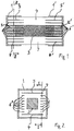
- the Figure 1 shows a cross section of an embodiment of the ceramic component.
- the main body 9 consists mainly of a ceramic material.
- an electrically active area 3 which essentially determines the function provided for the ceramic component and is constructed accordingly, and in particular can have internal electrodes.
- the active region 3 can be, for example, a stack of layers that are alternately made of metal and dielectric ceramic material.
- Other materials that can be used in the active region 3 are, for example, PTC material whose electrical resistance increases as the temperature increases, NTC material whose electrical resistance decreases as the temperature increases, varistor ceramic whose electrical resistance is voltage-dependent, Ferrite, semiconductor material, polymer or the like.
- the inner electrodes can be arranged, for example, overlapping one another or interdigitated in a comb-like manner. Such materials and arrangements are known per se from multilayer components.
- the base body 9 can in principle be of any shape, for example cuboid and in particular elongated.
- the active region 3 preferably extends in the longitudinal direction of the base body 9, which in the example of FIG Figure 1 runs horizontally.
- on the end faces of the base body 9 lying opposite one another in the longitudinal direction there are separate external contacts 1, 1 ', which are arranged on each of the end faces of the base body 9 and in particular can also cover the edges of the base body 9 there, as in FIG Figure 1 is shown.
- a respective lead area 2, 2' in which an electrically conductive connection between an electrical connection or internal electrodes of the active area 3 and the relevant external contact 1, 1 'runs.
- This electrically conductive connection can be formed by a simple electrical conductor, for example by a conductor strip which is structured in a metal layer, or also have a structure comprising a plurality of conductors, with which, for example, the lead resistance can be reduced.
- the hatching of the lead areas 2, 2 'and the active area 3 indicates in the figures that these areas have an internal structure corresponding to the intended function of the ceramic component.
- the feed areas 2, 2 'and the active area 3 are only shown schematically and do not have to assume the dimensions and limits shown in the figures.
- the Figure 2 shows the in the Figure 1 marked cross section.
- the external contact 1 is located on an end face of the base body 9 and, as in the example shown, can cover the edges of the base body 9 that border this end face on all sides, so that the external contact 1 in the region of the cross section according to FIG Figure 2 encloses the base body 9.
- the supply area 2 is located in the interior of the base body 9 at a distance from the outer sides of the base body 9 which are lateral with respect to the longitudinal direction and which adjoin the end face.
- the electrodes 4, 5, 6, 6 ′′ are arranged between these lateral outer sides and the lead area 2, which shield the lead area 2 and are electrically conductively connected to the external contact 1.
- the electrodes 4, 5, 6, 6 electrically conductively connected to the external contact 1 on the end face of the base body 9. It is also possible, instead or in addition, to have an electrically conductive connection between the electrodes 4, 5, 6, 6 "and the lateral one in the cross section of the Figure 2 Provide recognizable portion of the external contact 1.
- the electrodes 4, 5, 6, 6 " can be arranged at a distance from the lead area 2, as in FIG Figure 2 is recognizable.
- the electrodes 4, 5, 6, 6 " are designed as plates and are arranged coplanarly at a distance from one another and at least surround the lead area 2 in the lateral directions with respect to the longitudinal direction, that is to say where the lead area 2 does not contact the external contact 1 still adjoins the active area 3.
- the electrodes 4, 5, 6, 6 " can extend so far into the interior of the base body 9 that they also shield part of the active area 3.
- the in the Figure 2 lower electrode 4 and in the Figure 2 Upper electrode 5 are arranged in such a way that the planar expansion of these electrodes 4, 5 causes the supply area 2 to be shielded.
- the laterally arranged electrodes 6, 6 ′′ are arranged coplanar with the electrodes 4, 5 at the top and bottom at a sufficiently small distance from one another in accordance with a layer structure of the base body 9, so that they act as a Faraday cage and thus provide adequate shielding for the intended purpose ,
- the Figure 3 shows a cross section of a further exemplary embodiment, the further external contacts 1 ′′ (in Figure 4 shown) and 1 '''.
- the further external contacts 1 ′′, 1 ′ ′′ are arranged between the mutually opposite end faces of the base body 9 in an area that is central with respect to the longitudinal direction of the base body 9 and are separated from the already described external contacts 1, 1 ′ and are used in the following to distinguish them from those shown in FIGS End faces of the base body 9 arranged external contacts 1, 1 'referred to as the middle external contacts 1'',1'''.
- the Figure 4 shows the in the Figure 3 marked cross section. It can be seen that between the middle external contacts 1 ′′, 1 ′′ ′′ and the active area 3 there are further lead areas 2 ′′, 2 ′′ ′′, which connect the active area 3 with the relevant middle external contact 1 ′′, 1 '". Additional electrodes 7'',8'',7''', 8 '''provided for electrical shielding are adjacent to These middle supply areas 2 ′′, 2 ′′ ′′ are arranged and electrically conductively connected to the relevant middle external contact 1 ′′, 1 ′′.
- these middle electrodes 7 ′′, 8 ′′, 7 ′′ ′′, 8 “" in each case plates which are arranged above and below a layer position of the base body 9 which is taken up by the active region 3 and the central supply regions 2 "", 2 "".
- the central electrodes 7 ", 8", provided for shielding 7 ′′ ′′, 8 ′′ ′′ can be arranged within the base body 9 at a distance from the central feed regions 2 ′′, 2 ′′ ′′.
- the Figure 5 shows a cross section of a further embodiment, in which the arrangement of the shielding electrodes 4, 4 ', 5, 5' compared to the embodiment of FIG Figure 1 is simplified.
- the laterally arranged electrodes 6, 6 are omitted.
- the Figure 6 shows the in the Figure 5 marked cross section. This shows that, in this exemplary embodiment, shielding of the lead region 2 in two directions opposite to one another by means of that in FIG Figure 6 lower electrode 4 and in the Figure 6 upper electrode 5 is provided.
- the Figure 7 shows a cross section of another embodiment in which the arrangement of the shielding electrodes 4 ', 5, compared to the embodiment according to the Figure 5 is again simplified.
- the embodiment according to the Figure 7 there is only one upper shielding electrode 5 at one end of the base body 9 and only a lower one at the opposite end of the base body 9 shielding electrode 4 '.
- the laterally arranged electrodes 6, 6 are also omitted here.
- the Figure 8 shows the in the Figure 7 marked cross section. This shows that in this exemplary embodiment a shielding of the in the Figure 7 Supply area 2 shown on the left only by means of the in the Figure 8 upper electrode 5 is provided. A shield of the in the Figure 7 Correspondingly, the supply area 2 'shown on the right is only by means of the in the Figure 7 drawn lower electrode 4 'provided.
- a symmetry of the arrangement of the shielding electrodes 4, 4 ', 5, 5', 6, 6 ', 6'',7'',7''', 8 '', 8 ''' is related on the active area 3 and the lead areas 2, 2 ', 2'',2'"leading to the active area 3.
- This symmetry is present in the exemplary embodiments of FIGS Figures 1 to 6 a mirror symmetry and in the embodiment of the Figures 7 and 8 an axis symmetry with respect to a rotation through 180 °.
- the axis of symmetry is perpendicular to the plane of the drawing Figure 7 and runs through the center of the ceramic component.
Landscapes
- Engineering & Computer Science (AREA)
- Power Engineering (AREA)
- Microelectronics & Electronic Packaging (AREA)
- Manufacturing & Machinery (AREA)
- Physics & Mathematics (AREA)
- Electromagnetism (AREA)
- Thermistors And Varistors (AREA)
- Fixed Capacitors And Capacitor Manufacturing Machines (AREA)
- Ceramic Capacitors (AREA)
Applications Claiming Priority (2)
| Application Number | Priority Date | Filing Date | Title |
|---|---|---|---|
| DE102011010611A DE102011010611A1 (de) | 2011-02-08 | 2011-02-08 | Elektrisches Keramikbauelement mit elektrischer Abschirmung |
| PCT/EP2012/051786 WO2012107349A1 (de) | 2011-02-08 | 2012-02-02 | Elektrisches keramikbauelement mit elektrischer abschirmung |
Publications (2)
| Publication Number | Publication Date |
|---|---|
| EP2673787A1 EP2673787A1 (de) | 2013-12-18 |
| EP2673787B1 true EP2673787B1 (de) | 2020-01-01 |
Family
ID=45558740
Family Applications (1)
| Application Number | Title | Priority Date | Filing Date |
|---|---|---|---|
| EP12701912.3A Active EP2673787B1 (de) | 2011-02-08 | 2012-02-02 | Elektrisches keramikbauelement mit elektrischer abschirmung |
Country Status (7)
Families Citing this family (9)
| Publication number | Priority date | Publication date | Assignee | Title |
|---|---|---|---|---|
| JP3327474B2 (ja) | 1992-03-26 | 2002-09-24 | 株式会社サトー | 自動ラベル貼付け装置 |
| US10269493B2 (en) * | 2009-04-05 | 2019-04-23 | David Frank | Modular dense energy ultra cell and process for fabrication |
| JP2014027255A (ja) * | 2012-06-22 | 2014-02-06 | Murata Mfg Co Ltd | セラミック電子部品及びセラミック電子装置 |
| DE102013102686A1 (de) | 2013-03-15 | 2014-09-18 | Epcos Ag | Elektronisches Bauelement |
| DE102013012733A1 (de) * | 2013-07-31 | 2015-02-05 | Forschungszentrum Jülich GmbH | Widerstand mit verminderter parasitärer Kapazität |
| JP6694235B2 (ja) * | 2015-01-29 | 2020-05-13 | Tdk株式会社 | 電子部品 |
| WO2019053954A1 (ja) * | 2017-09-12 | 2019-03-21 | 株式会社村田製作所 | 積層コンデンサおよび回路モジュール |
| DE102019100316A1 (de) * | 2019-01-08 | 2020-07-09 | Tdk Electronics Ag | Thermistor und Verfahren zur Herstellung des Thermistors |
| CN113330527B (zh) * | 2019-01-28 | 2022-07-05 | 京瓷Avx元器件公司 | 具有超宽带性能的多层陶瓷电容器 |
Citations (2)
| Publication number | Priority date | Publication date | Assignee | Title |
|---|---|---|---|---|
| JP2000133545A (ja) * | 1998-10-26 | 2000-05-12 | Tdk Corp | 積層セラミックチップコンデンサ |
| DE10354026A1 (de) * | 2002-12-27 | 2004-07-22 | Murata Mfg. Co., Ltd., Nagaokakyo | Piezoelektrische Membran und diese piezoelektrischer elektroakustischer Wandler unter Verwendung derselben |
Family Cites Families (14)
| Publication number | Priority date | Publication date | Assignee | Title |
|---|---|---|---|---|
| JP3832504B2 (ja) | 2004-12-24 | 2006-10-11 | 株式会社村田製作所 | 積層コンデンサおよびその実装構造 |
| JP4803039B2 (ja) | 2005-01-06 | 2011-10-26 | 株式会社村田製作所 | 圧電アクチュエータの製造方法及び圧電アクチュエータ |
| DE102005033085A1 (de) * | 2005-07-15 | 2007-01-25 | Robert Bosch Gmbh | Piezoaktor |
| JP2007042743A (ja) * | 2005-08-01 | 2007-02-15 | Tdk Corp | 積層電子部品 |
| US7336475B2 (en) | 2006-02-22 | 2008-02-26 | Vishay Vitramon, Inc. | High voltage capacitors |
| DE102007020783A1 (de) | 2007-05-03 | 2008-11-06 | Epcos Ag | Elektrisches Vielschichtbauelement |
| KR100925623B1 (ko) | 2007-08-31 | 2009-11-06 | 삼성전기주식회사 | 적층형 칩 커패시터 및 이를 구비한 회로기판 장치 및회로기판 |
| KR100916476B1 (ko) * | 2007-11-30 | 2009-09-08 | 삼성전기주식회사 | 적층형 칩 커패시터 및 이를 구비한 회로기판 장치 |
| US8125762B2 (en) | 2008-08-11 | 2012-02-28 | Vishay Sprague, Inc. | High voltage capacitors |
| JP4905498B2 (ja) | 2009-04-22 | 2012-03-28 | 株式会社村田製作所 | 積層型セラミック電子部品 |
| JP5533387B2 (ja) * | 2010-07-21 | 2014-06-25 | 株式会社村田製作所 | セラミック電子部品 |
| JP2012156193A (ja) * | 2011-01-24 | 2012-08-16 | Tdk Corp | 積層コンデンサ |
| JP2012156315A (ja) | 2011-01-26 | 2012-08-16 | Murata Mfg Co Ltd | 積層セラミック電子部品 |
| KR101580349B1 (ko) * | 2012-01-31 | 2015-12-24 | 삼성전기주식회사 | 적층 세라믹 전자 부품 및 그 제조 방법 |
-
2011
- 2011-02-08 DE DE102011010611A patent/DE102011010611A1/de not_active Withdrawn
-
2012
- 2012-02-02 US US13/984,274 patent/US9338913B2/en active Active
- 2012-02-02 JP JP2013552909A patent/JP5913377B2/ja active Active
- 2012-02-02 KR KR1020137023857A patent/KR101543140B1/ko active Active
- 2012-02-02 CN CN201280008115.4A patent/CN103348419B/zh active Active
- 2012-02-02 EP EP12701912.3A patent/EP2673787B1/de active Active
- 2012-02-02 WO PCT/EP2012/051786 patent/WO2012107349A1/de active Application Filing
Patent Citations (2)
| Publication number | Priority date | Publication date | Assignee | Title |
|---|---|---|---|---|
| JP2000133545A (ja) * | 1998-10-26 | 2000-05-12 | Tdk Corp | 積層セラミックチップコンデンサ |
| DE10354026A1 (de) * | 2002-12-27 | 2004-07-22 | Murata Mfg. Co., Ltd., Nagaokakyo | Piezoelektrische Membran und diese piezoelektrischer elektroakustischer Wandler unter Verwendung derselben |
Also Published As
| Publication number | Publication date |
|---|---|
| DE102011010611A8 (de) | 2012-10-18 |
| US9338913B2 (en) | 2016-05-10 |
| CN103348419B (zh) | 2016-05-25 |
| KR101543140B1 (ko) | 2015-08-07 |
| EP2673787A1 (de) | 2013-12-18 |
| CN103348419A (zh) | 2013-10-09 |
| JP5913377B2 (ja) | 2016-04-27 |
| US20140041931A1 (en) | 2014-02-13 |
| JP2014508410A (ja) | 2014-04-03 |
| DE102011010611A1 (de) | 2012-08-09 |
| KR20130128456A (ko) | 2013-11-26 |
| WO2012107349A1 (de) | 2012-08-16 |
Similar Documents
| Publication | Publication Date | Title |
|---|---|---|
| EP2673787B1 (de) | Elektrisches keramikbauelement mit elektrischer abschirmung | |
| EP2143117B1 (de) | Elektrisches vielschichtbauelement mit elektrisch nicht kontaktierter abschirmstruktur | |
| EP2174328B1 (de) | elektrisches Vielschichtbauelement mit einem Widerstand und einer Entkopplungsschicht | |
| EP2614508B1 (de) | Widerstandsbauelement und verfahren zur herstellung eines widerstandsbauelements | |
| DE102009010212B4 (de) | Elektrisches Vielschichtbauelement | |
| DE102007044604A1 (de) | Elektrisches Vielschichtbauelement | |
| WO2014139696A1 (de) | Elektronisches bauelement | |
| EP2612333B1 (de) | Keramisches bauelement und verfahren zur herstellung eines keramischen bauelements | |
| EP2636047A2 (de) | Keramisches vielschichtbauelement und verfahren zur herstellung eines keramischen vielschichtbauelements | |
| DE112011105495T5 (de) | Sensorvorrichtung | |
| DE102005028498A1 (de) | Elektrisches Vielschichtbauelement | |
| WO2020007864A1 (de) | Vielschichtvaristor mit feldoptimiertem mikrogefüge | |
| EP2976773A1 (de) | Gekapselter überspannungsableiter | |
| DE112020005494T5 (de) | Varistor | |
| DE102007044453A1 (de) | Elektrisches Vielschichtbauelement | |
| EP2392057B1 (de) | Überspannungsableiter | |
| DE3702780A1 (de) | Integrierte Varistor-Schutzvorrichtung zum Schutz eines Elektronikbauteils gegen die Wirkungen von elektromagnetischen Feldern oder statischen Ladungen | |
| EP3364181B1 (de) | Feuchtesensoranordnung mit esd-schutz | |
| DE10134751C1 (de) | Elektrokeramisches Bauelement | |
| EP2465123B1 (de) | Elektrisches vielschichtbauelement | |
| EP1911052B1 (de) | Elektrisches bauelement | |
| DE112022003846T5 (de) | Folienkondensator | |
| DE102025106368A1 (de) | Elektronisches bauteil | |
| DE102021103424A1 (de) | Mikroelektronische Vorrichtungen | |
| DE102012105517A1 (de) | Vielschichtbauelement mit einer Außenkontaktierung und Verfahren zur Herstellung eines Vielschichtbauelements mit einer Außenkontaktierung |
Legal Events
| Date | Code | Title | Description |
|---|---|---|---|
| PUAI | Public reference made under article 153(3) epc to a published international application that has entered the european phase |
Free format text: ORIGINAL CODE: 0009012 |
|
| 17P | Request for examination filed |
Effective date: 20130702 |
|
| AK | Designated contracting states |
Kind code of ref document: A1 Designated state(s): AL AT BE BG CH CY CZ DE DK EE ES FI FR GB GR HR HU IE IS IT LI LT LU LV MC MK MT NL NO PL PT RO RS SE SI SK SM TR |
|
| DAX | Request for extension of the european patent (deleted) | ||
| 17Q | First examination report despatched |
Effective date: 20140623 |
|
| STAA | Information on the status of an ep patent application or granted ep patent |
Free format text: STATUS: EXAMINATION IS IN PROGRESS |
|
| RAP1 | Party data changed (applicant data changed or rights of an application transferred) |
Owner name: EPCOS AG |
|
| RAP1 | Party data changed (applicant data changed or rights of an application transferred) |
Owner name: TDK ELECTRONICS AG |
|
| GRAP | Despatch of communication of intention to grant a patent |
Free format text: ORIGINAL CODE: EPIDOSNIGR1 |
|
| STAA | Information on the status of an ep patent application or granted ep patent |
Free format text: STATUS: GRANT OF PATENT IS INTENDED |
|
| INTG | Intention to grant announced |
Effective date: 20191011 |
|
| GRAS | Grant fee paid |
Free format text: ORIGINAL CODE: EPIDOSNIGR3 |
|
| GRAA | (expected) grant |
Free format text: ORIGINAL CODE: 0009210 |
|
| STAA | Information on the status of an ep patent application or granted ep patent |
Free format text: STATUS: THE PATENT HAS BEEN GRANTED |
|
| AK | Designated contracting states |
Kind code of ref document: B1 Designated state(s): AL AT BE BG CH CY CZ DE DK EE ES FI FR GB GR HR HU IE IS IT LI LT LU LV MC MK MT NL NO PL PT RO RS SE SI SK SM TR |
|
| REG | Reference to a national code |
Ref country code: GB Ref legal event code: FG4D Free format text: NOT ENGLISH |
|
| REG | Reference to a national code |
Ref country code: CH Ref legal event code: EP Ref country code: AT Ref legal event code: REF Ref document number: 1220825 Country of ref document: AT Kind code of ref document: T Effective date: 20200115 |
|
| REG | Reference to a national code |
Ref country code: DE Ref legal event code: R096 Ref document number: 502012015658 Country of ref document: DE |
|
| REG | Reference to a national code |
Ref country code: IE Ref legal event code: FG4D Free format text: LANGUAGE OF EP DOCUMENT: GERMAN |
|
| REG | Reference to a national code |
Ref country code: NL Ref legal event code: MP Effective date: 20200101 |
|
| REG | Reference to a national code |
Ref country code: LT Ref legal event code: MG4D |
|
| PG25 | Lapsed in a contracting state [announced via postgrant information from national office to epo] |
Ref country code: FI Free format text: LAPSE BECAUSE OF FAILURE TO SUBMIT A TRANSLATION OF THE DESCRIPTION OR TO PAY THE FEE WITHIN THE PRESCRIBED TIME-LIMIT Effective date: 20200101 Ref country code: PT Free format text: LAPSE BECAUSE OF FAILURE TO SUBMIT A TRANSLATION OF THE DESCRIPTION OR TO PAY THE FEE WITHIN THE PRESCRIBED TIME-LIMIT Effective date: 20200527 Ref country code: CZ Free format text: LAPSE BECAUSE OF FAILURE TO SUBMIT A TRANSLATION OF THE DESCRIPTION OR TO PAY THE FEE WITHIN THE PRESCRIBED TIME-LIMIT Effective date: 20200101 Ref country code: NO Free format text: LAPSE BECAUSE OF FAILURE TO SUBMIT A TRANSLATION OF THE DESCRIPTION OR TO PAY THE FEE WITHIN THE PRESCRIBED TIME-LIMIT Effective date: 20200401 Ref country code: LT Free format text: LAPSE BECAUSE OF FAILURE TO SUBMIT A TRANSLATION OF THE DESCRIPTION OR TO PAY THE FEE WITHIN THE PRESCRIBED TIME-LIMIT Effective date: 20200101 Ref country code: NL Free format text: LAPSE BECAUSE OF FAILURE TO SUBMIT A TRANSLATION OF THE DESCRIPTION OR TO PAY THE FEE WITHIN THE PRESCRIBED TIME-LIMIT Effective date: 20200101 Ref country code: RS Free format text: LAPSE BECAUSE OF FAILURE TO SUBMIT A TRANSLATION OF THE DESCRIPTION OR TO PAY THE FEE WITHIN THE PRESCRIBED TIME-LIMIT Effective date: 20200101 |
|
| PG25 | Lapsed in a contracting state [announced via postgrant information from national office to epo] |
Ref country code: GR Free format text: LAPSE BECAUSE OF FAILURE TO SUBMIT A TRANSLATION OF THE DESCRIPTION OR TO PAY THE FEE WITHIN THE PRESCRIBED TIME-LIMIT Effective date: 20200402 Ref country code: IS Free format text: LAPSE BECAUSE OF FAILURE TO SUBMIT A TRANSLATION OF THE DESCRIPTION OR TO PAY THE FEE WITHIN THE PRESCRIBED TIME-LIMIT Effective date: 20200501 Ref country code: HR Free format text: LAPSE BECAUSE OF FAILURE TO SUBMIT A TRANSLATION OF THE DESCRIPTION OR TO PAY THE FEE WITHIN THE PRESCRIBED TIME-LIMIT Effective date: 20200101 Ref country code: LV Free format text: LAPSE BECAUSE OF FAILURE TO SUBMIT A TRANSLATION OF THE DESCRIPTION OR TO PAY THE FEE WITHIN THE PRESCRIBED TIME-LIMIT Effective date: 20200101 Ref country code: SE Free format text: LAPSE BECAUSE OF FAILURE TO SUBMIT A TRANSLATION OF THE DESCRIPTION OR TO PAY THE FEE WITHIN THE PRESCRIBED TIME-LIMIT Effective date: 20200101 Ref country code: BG Free format text: LAPSE BECAUSE OF FAILURE TO SUBMIT A TRANSLATION OF THE DESCRIPTION OR TO PAY THE FEE WITHIN THE PRESCRIBED TIME-LIMIT Effective date: 20200401 |
|
| REG | Reference to a national code |
Ref country code: CH Ref legal event code: PL |
|
| REG | Reference to a national code |
Ref country code: DE Ref legal event code: R097 Ref document number: 502012015658 Country of ref document: DE |
|
| REG | Reference to a national code |
Ref country code: BE Ref legal event code: MM Effective date: 20200229 |
|
| PG25 | Lapsed in a contracting state [announced via postgrant information from national office to epo] |
Ref country code: MC Free format text: LAPSE BECAUSE OF FAILURE TO SUBMIT A TRANSLATION OF THE DESCRIPTION OR TO PAY THE FEE WITHIN THE PRESCRIBED TIME-LIMIT Effective date: 20200101 Ref country code: ES Free format text: LAPSE BECAUSE OF FAILURE TO SUBMIT A TRANSLATION OF THE DESCRIPTION OR TO PAY THE FEE WITHIN THE PRESCRIBED TIME-LIMIT Effective date: 20200101 Ref country code: RO Free format text: LAPSE BECAUSE OF FAILURE TO SUBMIT A TRANSLATION OF THE DESCRIPTION OR TO PAY THE FEE WITHIN THE PRESCRIBED TIME-LIMIT Effective date: 20200101 Ref country code: LU Free format text: LAPSE BECAUSE OF NON-PAYMENT OF DUE FEES Effective date: 20200202 Ref country code: EE Free format text: LAPSE BECAUSE OF FAILURE TO SUBMIT A TRANSLATION OF THE DESCRIPTION OR TO PAY THE FEE WITHIN THE PRESCRIBED TIME-LIMIT Effective date: 20200101 Ref country code: SM Free format text: LAPSE BECAUSE OF FAILURE TO SUBMIT A TRANSLATION OF THE DESCRIPTION OR TO PAY THE FEE WITHIN THE PRESCRIBED TIME-LIMIT Effective date: 20200101 Ref country code: DK Free format text: LAPSE BECAUSE OF FAILURE TO SUBMIT A TRANSLATION OF THE DESCRIPTION OR TO PAY THE FEE WITHIN THE PRESCRIBED TIME-LIMIT Effective date: 20200101 Ref country code: SK Free format text: LAPSE BECAUSE OF FAILURE TO SUBMIT A TRANSLATION OF THE DESCRIPTION OR TO PAY THE FEE WITHIN THE PRESCRIBED TIME-LIMIT Effective date: 20200101 |
|
| PLBE | No opposition filed within time limit |
Free format text: ORIGINAL CODE: 0009261 |
|
| STAA | Information on the status of an ep patent application or granted ep patent |
Free format text: STATUS: NO OPPOSITION FILED WITHIN TIME LIMIT |
|
| PG25 | Lapsed in a contracting state [announced via postgrant information from national office to epo] |
Ref country code: CH Free format text: LAPSE BECAUSE OF NON-PAYMENT OF DUE FEES Effective date: 20200229 Ref country code: LI Free format text: LAPSE BECAUSE OF NON-PAYMENT OF DUE FEES Effective date: 20200229 |
|
| 26N | No opposition filed |
Effective date: 20201002 |
|
| PG25 | Lapsed in a contracting state [announced via postgrant information from national office to epo] |
Ref country code: FR Free format text: LAPSE BECAUSE OF NON-PAYMENT OF DUE FEES Effective date: 20200301 Ref country code: IE Free format text: LAPSE BECAUSE OF NON-PAYMENT OF DUE FEES Effective date: 20200202 Ref country code: IT Free format text: LAPSE BECAUSE OF FAILURE TO SUBMIT A TRANSLATION OF THE DESCRIPTION OR TO PAY THE FEE WITHIN THE PRESCRIBED TIME-LIMIT Effective date: 20200101 |
|
| PG25 | Lapsed in a contracting state [announced via postgrant information from national office to epo] |
Ref country code: PL Free format text: LAPSE BECAUSE OF FAILURE TO SUBMIT A TRANSLATION OF THE DESCRIPTION OR TO PAY THE FEE WITHIN THE PRESCRIBED TIME-LIMIT Effective date: 20200101 Ref country code: BE Free format text: LAPSE BECAUSE OF NON-PAYMENT OF DUE FEES Effective date: 20200229 Ref country code: SI Free format text: LAPSE BECAUSE OF FAILURE TO SUBMIT A TRANSLATION OF THE DESCRIPTION OR TO PAY THE FEE WITHIN THE PRESCRIBED TIME-LIMIT Effective date: 20200101 |
|
| GBPC | Gb: european patent ceased through non-payment of renewal fee |
Effective date: 20200401 |
|
| REG | Reference to a national code |
Ref country code: AT Ref legal event code: MM01 Ref document number: 1220825 Country of ref document: AT Kind code of ref document: T Effective date: 20200202 |
|
| PG25 | Lapsed in a contracting state [announced via postgrant information from national office to epo] |
Ref country code: GB Free format text: LAPSE BECAUSE OF NON-PAYMENT OF DUE FEES Effective date: 20200401 |
|
| PG25 | Lapsed in a contracting state [announced via postgrant information from national office to epo] |
Ref country code: AT Free format text: LAPSE BECAUSE OF NON-PAYMENT OF DUE FEES Effective date: 20200202 |
|
| PG25 | Lapsed in a contracting state [announced via postgrant information from national office to epo] |
Ref country code: TR Free format text: LAPSE BECAUSE OF FAILURE TO SUBMIT A TRANSLATION OF THE DESCRIPTION OR TO PAY THE FEE WITHIN THE PRESCRIBED TIME-LIMIT Effective date: 20200101 Ref country code: MT Free format text: LAPSE BECAUSE OF FAILURE TO SUBMIT A TRANSLATION OF THE DESCRIPTION OR TO PAY THE FEE WITHIN THE PRESCRIBED TIME-LIMIT Effective date: 20200101 Ref country code: CY Free format text: LAPSE BECAUSE OF FAILURE TO SUBMIT A TRANSLATION OF THE DESCRIPTION OR TO PAY THE FEE WITHIN THE PRESCRIBED TIME-LIMIT Effective date: 20200101 |
|
| PG25 | Lapsed in a contracting state [announced via postgrant information from national office to epo] |
Ref country code: MK Free format text: LAPSE BECAUSE OF FAILURE TO SUBMIT A TRANSLATION OF THE DESCRIPTION OR TO PAY THE FEE WITHIN THE PRESCRIBED TIME-LIMIT Effective date: 20200101 Ref country code: AL Free format text: LAPSE BECAUSE OF FAILURE TO SUBMIT A TRANSLATION OF THE DESCRIPTION OR TO PAY THE FEE WITHIN THE PRESCRIBED TIME-LIMIT Effective date: 20200101 |
|
| P01 | Opt-out of the competence of the unified patent court (upc) registered |
Effective date: 20230521 |
|
| PGFP | Annual fee paid to national office [announced via postgrant information from national office to epo] |
Ref country code: DE Payment date: 20250220 Year of fee payment: 14 |