EP2668683B1 - Batterie améliorée et procédé d'assemblage - Google Patents
Batterie améliorée et procédé d'assemblage Download PDFInfo
- Publication number
- EP2668683B1 EP2668683B1 EP12722634.8A EP12722634A EP2668683B1 EP 2668683 B1 EP2668683 B1 EP 2668683B1 EP 12722634 A EP12722634 A EP 12722634A EP 2668683 B1 EP2668683 B1 EP 2668683B1
- Authority
- EP
- European Patent Office
- Prior art keywords
- battery
- silicon wafer
- active material
- stack
- conductive silicon
- Prior art date
- Legal status (The legal status is an assumption and is not a legal conclusion. Google has not performed a legal analysis and makes no representation as to the accuracy of the status listed.)
- Active
Links
- 238000000034 method Methods 0.000 title claims description 48
- XUIMIQQOPSSXEZ-UHFFFAOYSA-N Silicon Chemical compound [Si] XUIMIQQOPSSXEZ-UHFFFAOYSA-N 0.000 claims description 58
- 229910052710 silicon Inorganic materials 0.000 claims description 58
- 239000010703 silicon Substances 0.000 claims description 58
- 235000012431 wafers Nutrition 0.000 claims description 47
- 239000003792 electrolyte Substances 0.000 claims description 42
- QAOWNCQODCNURD-UHFFFAOYSA-N Sulfuric acid Chemical compound OS(O)(=O)=O QAOWNCQODCNURD-UHFFFAOYSA-N 0.000 claims description 38
- 239000011149 active material Substances 0.000 claims description 33
- 239000000463 material Substances 0.000 claims description 32
- 239000011159 matrix material Substances 0.000 claims description 29
- 239000011248 coating agent Substances 0.000 claims description 28
- 238000000576 coating method Methods 0.000 claims description 28
- PXHVJJICTQNCMI-UHFFFAOYSA-N Nickel Chemical compound [Ni] PXHVJJICTQNCMI-UHFFFAOYSA-N 0.000 claims description 27
- 239000002245 particle Substances 0.000 claims description 23
- FVBUAEGBCNSCDD-UHFFFAOYSA-N silicide(4-) Chemical compound [Si-4] FVBUAEGBCNSCDD-UHFFFAOYSA-N 0.000 claims description 22
- 238000000151 deposition Methods 0.000 claims description 19
- 229910021332 silicide Inorganic materials 0.000 claims description 17
- 239000011148 porous material Substances 0.000 claims description 16
- 238000007747 plating Methods 0.000 claims description 15
- 229910052759 nickel Inorganic materials 0.000 claims description 13
- 230000004888 barrier function Effects 0.000 claims description 12
- YADSGOSSYOOKMP-UHFFFAOYSA-N dioxolead Chemical compound O=[Pb]=O YADSGOSSYOOKMP-UHFFFAOYSA-N 0.000 claims description 10
- ATJFFYVFTNAWJD-UHFFFAOYSA-N Tin Chemical compound [Sn] ATJFFYVFTNAWJD-UHFFFAOYSA-N 0.000 claims description 6
- 238000001704 evaporation Methods 0.000 claims description 5
- 238000010438 heat treatment Methods 0.000 claims description 5
- 238000004544 sputter deposition Methods 0.000 claims description 4
- VYZAMTAEIAYCRO-UHFFFAOYSA-N Chromium Chemical compound [Cr] VYZAMTAEIAYCRO-UHFFFAOYSA-N 0.000 claims description 3
- ZOKXTWBITQBERF-UHFFFAOYSA-N Molybdenum Chemical compound [Mo] ZOKXTWBITQBERF-UHFFFAOYSA-N 0.000 claims description 3
- RTAQQCXQSZGOHL-UHFFFAOYSA-N Titanium Chemical compound [Ti] RTAQQCXQSZGOHL-UHFFFAOYSA-N 0.000 claims description 3
- 229910052750 molybdenum Inorganic materials 0.000 claims description 3
- 239000011733 molybdenum Substances 0.000 claims description 3
- MHWZQNGIEIYAQJ-UHFFFAOYSA-N molybdenum diselenide Chemical compound [Se]=[Mo]=[Se] MHWZQNGIEIYAQJ-UHFFFAOYSA-N 0.000 claims description 3
- 238000007789 sealing Methods 0.000 claims description 3
- 229910052719 titanium Inorganic materials 0.000 claims description 3
- 239000010936 titanium Substances 0.000 claims description 3
- WFKWXMTUELFFGS-UHFFFAOYSA-N tungsten Chemical compound [W] WFKWXMTUELFFGS-UHFFFAOYSA-N 0.000 claims description 3
- 229910052721 tungsten Inorganic materials 0.000 claims description 3
- 239000010937 tungsten Substances 0.000 claims description 3
- 229910052751 metal Inorganic materials 0.000 claims description 2
- 239000002184 metal Substances 0.000 claims description 2
- 239000010410 layer Substances 0.000 description 78
- 125000006850 spacer group Chemical group 0.000 description 52
- 239000000758 substrate Substances 0.000 description 41
- 239000002253 acid Substances 0.000 description 36
- 230000008569 process Effects 0.000 description 18
- 229910000464 lead oxide Inorganic materials 0.000 description 15
- YEXPOXQUZXUXJW-UHFFFAOYSA-N oxolead Chemical compound [Pb]=O YEXPOXQUZXUXJW-UHFFFAOYSA-N 0.000 description 15
- 239000000853 adhesive Substances 0.000 description 14
- 230000001070 adhesive effect Effects 0.000 description 14
- 238000006243 chemical reaction Methods 0.000 description 13
- 239000011152 fibreglass Substances 0.000 description 13
- 239000000203 mixture Substances 0.000 description 11
- 230000008021 deposition Effects 0.000 description 10
- 150000002500 ions Chemical class 0.000 description 10
- 239000004033 plastic Substances 0.000 description 10
- 229920003023 plastic Polymers 0.000 description 10
- OKTJSMMVPCPJKN-UHFFFAOYSA-N Carbon Chemical compound [C] OKTJSMMVPCPJKN-UHFFFAOYSA-N 0.000 description 9
- 238000013459 approach Methods 0.000 description 9
- 229910052799 carbon Inorganic materials 0.000 description 9
- PIJPYDMVFNTHIP-UHFFFAOYSA-L lead sulfate Chemical compound [PbH4+2].[O-]S([O-])(=O)=O PIJPYDMVFNTHIP-UHFFFAOYSA-L 0.000 description 8
- 239000004593 Epoxy Substances 0.000 description 7
- 238000004519 manufacturing process Methods 0.000 description 7
- 150000003839 salts Chemical class 0.000 description 7
- LFQSCWFLJHTTHZ-UHFFFAOYSA-N Ethanol Chemical compound CCO LFQSCWFLJHTTHZ-UHFFFAOYSA-N 0.000 description 6
- KRHYYFGTRYWZRS-UHFFFAOYSA-N Fluorane Chemical compound F KRHYYFGTRYWZRS-UHFFFAOYSA-N 0.000 description 6
- HBBGRARXTFLTSG-UHFFFAOYSA-N Lithium ion Chemical compound [Li+] HBBGRARXTFLTSG-UHFFFAOYSA-N 0.000 description 6
- KWYUFKZDYYNOTN-UHFFFAOYSA-M Potassium hydroxide Chemical compound [OH-].[K+] KWYUFKZDYYNOTN-UHFFFAOYSA-M 0.000 description 6
- 230000008901 benefit Effects 0.000 description 6
- 238000001962 electrophoresis Methods 0.000 description 6
- 229910001416 lithium ion Inorganic materials 0.000 description 6
- 230000015572 biosynthetic process Effects 0.000 description 5
- 239000004020 conductor Substances 0.000 description 5
- 239000013078 crystal Substances 0.000 description 5
- 238000006722 reduction reaction Methods 0.000 description 5
- 239000000243 solution Substances 0.000 description 5
- FAPWRFPIFSIZLT-UHFFFAOYSA-M Sodium chloride Chemical compound [Na+].[Cl-] FAPWRFPIFSIZLT-UHFFFAOYSA-M 0.000 description 4
- 230000001351 cycling effect Effects 0.000 description 4
- 238000013461 design Methods 0.000 description 4
- RUFLMLWJRZAWLJ-UHFFFAOYSA-N nickel silicide Chemical compound [Ni]=[Si]=[Ni] RUFLMLWJRZAWLJ-UHFFFAOYSA-N 0.000 description 4
- 229910021334 nickel silicide Inorganic materials 0.000 description 4
- 239000012188 paraffin wax Substances 0.000 description 4
- 239000000565 sealant Substances 0.000 description 4
- 238000000926 separation method Methods 0.000 description 4
- UFHFLCQGNIYNRP-UHFFFAOYSA-N Hydrogen Chemical compound [H][H] UFHFLCQGNIYNRP-UHFFFAOYSA-N 0.000 description 3
- 239000000654 additive Substances 0.000 description 3
- 230000001143 conditioned effect Effects 0.000 description 3
- 238000005260 corrosion Methods 0.000 description 3
- 230000007797 corrosion Effects 0.000 description 3
- -1 electronic Chemical compound 0.000 description 3
- 238000001652 electrophoretic deposition Methods 0.000 description 3
- 238000005516 engineering process Methods 0.000 description 3
- 230000008020 evaporation Effects 0.000 description 3
- 239000010408 film Substances 0.000 description 3
- 230000006870 function Effects 0.000 description 3
- 229910052739 hydrogen Inorganic materials 0.000 description 3
- 239000001257 hydrogen Substances 0.000 description 3
- 230000015654 memory Effects 0.000 description 3
- 230000000704 physical effect Effects 0.000 description 3
- 230000009467 reduction Effects 0.000 description 3
- MHAJPDPJQMAIIY-UHFFFAOYSA-N Hydrogen peroxide Chemical compound OO MHAJPDPJQMAIIY-UHFFFAOYSA-N 0.000 description 2
- WHXSMMKQMYFTQS-UHFFFAOYSA-N Lithium Chemical compound [Li] WHXSMMKQMYFTQS-UHFFFAOYSA-N 0.000 description 2
- 239000004809 Teflon Substances 0.000 description 2
- 229920006362 Teflon® Polymers 0.000 description 2
- GWEVSGVZZGPLCZ-UHFFFAOYSA-N Titan oxide Chemical compound O=[Ti]=O GWEVSGVZZGPLCZ-UHFFFAOYSA-N 0.000 description 2
- 230000000996 additive effect Effects 0.000 description 2
- 229910045601 alloy Inorganic materials 0.000 description 2
- 239000000956 alloy Substances 0.000 description 2
- 230000009286 beneficial effect Effects 0.000 description 2
- 230000015556 catabolic process Effects 0.000 description 2
- 239000000919 ceramic Substances 0.000 description 2
- 230000003750 conditioning effect Effects 0.000 description 2
- 238000001816 cooling Methods 0.000 description 2
- 230000007423 decrease Effects 0.000 description 2
- 238000006731 degradation reaction Methods 0.000 description 2
- 238000007599 discharging Methods 0.000 description 2
- 238000009826 distribution Methods 0.000 description 2
- 230000000694 effects Effects 0.000 description 2
- 238000004146 energy storage Methods 0.000 description 2
- 239000007789 gas Substances 0.000 description 2
- 238000009830 intercalation Methods 0.000 description 2
- 230000002687 intercalation Effects 0.000 description 2
- KFZMGEQAYNKOFK-UHFFFAOYSA-N isopropyl alcohol Natural products CC(C)O KFZMGEQAYNKOFK-UHFFFAOYSA-N 0.000 description 2
- 229910052744 lithium Inorganic materials 0.000 description 2
- 238000001000 micrograph Methods 0.000 description 2
- 229920000642 polymer Polymers 0.000 description 2
- 229920001296 polysiloxane Polymers 0.000 description 2
- 238000007665 sagging Methods 0.000 description 2
- 238000005488 sandblasting Methods 0.000 description 2
- 239000003566 sealing material Substances 0.000 description 2
- 239000002356 single layer Substances 0.000 description 2
- 239000011780 sodium chloride Substances 0.000 description 2
- 239000007787 solid Substances 0.000 description 2
- 239000000126 substance Substances 0.000 description 2
- 239000000725 suspension Substances 0.000 description 2
- 239000010409 thin film Substances 0.000 description 2
- 239000001993 wax Substances 0.000 description 2
- ZOXJGFHDIHLPTG-UHFFFAOYSA-N Boron Chemical compound [B] ZOXJGFHDIHLPTG-UHFFFAOYSA-N 0.000 description 1
- GRYLNZFGIOXLOG-UHFFFAOYSA-N Nitric acid Chemical compound O[N+]([O-])=O GRYLNZFGIOXLOG-UHFFFAOYSA-N 0.000 description 1
- OAICVXFJPJFONN-UHFFFAOYSA-N Phosphorus Chemical compound [P] OAICVXFJPJFONN-UHFFFAOYSA-N 0.000 description 1
- 239000004743 Polypropylene Substances 0.000 description 1
- 238000010521 absorption reaction Methods 0.000 description 1
- 238000013019 agitation Methods 0.000 description 1
- 229910052782 aluminium Inorganic materials 0.000 description 1
- XAGFODPZIPBFFR-UHFFFAOYSA-N aluminium Chemical compound [Al] XAGFODPZIPBFFR-UHFFFAOYSA-N 0.000 description 1
- 229910052787 antimony Inorganic materials 0.000 description 1
- WATWJIUSRGPENY-UHFFFAOYSA-N antimony atom Chemical compound [Sb] WATWJIUSRGPENY-UHFFFAOYSA-N 0.000 description 1
- 229910052785 arsenic Inorganic materials 0.000 description 1
- RQNWIZPPADIBDY-UHFFFAOYSA-N arsenic atom Chemical compound [As] RQNWIZPPADIBDY-UHFFFAOYSA-N 0.000 description 1
- 239000011230 binding agent Substances 0.000 description 1
- 229910052796 boron Inorganic materials 0.000 description 1
- 239000003990 capacitor Substances 0.000 description 1
- 239000007795 chemical reaction product Substances 0.000 description 1
- 238000004140 cleaning Methods 0.000 description 1
- 238000010960 commercial process Methods 0.000 description 1
- 150000001875 compounds Chemical class 0.000 description 1
- 238000004590 computer program Methods 0.000 description 1
- 239000000470 constituent Substances 0.000 description 1
- 238000011109 contamination Methods 0.000 description 1
- 230000008878 coupling Effects 0.000 description 1
- 238000010168 coupling process Methods 0.000 description 1
- 238000005859 coupling reaction Methods 0.000 description 1
- 238000000354 decomposition reaction Methods 0.000 description 1
- 230000003247 decreasing effect Effects 0.000 description 1
- 230000007547 defect Effects 0.000 description 1
- 230000032798 delamination Effects 0.000 description 1
- 238000005137 deposition process Methods 0.000 description 1
- 238000009792 diffusion process Methods 0.000 description 1
- 238000007598 dipping method Methods 0.000 description 1
- 239000002019 doping agent Substances 0.000 description 1
- 230000005611 electricity Effects 0.000 description 1
- 239000008151 electrolyte solution Substances 0.000 description 1
- 239000000835 fiber Substances 0.000 description 1
- 239000000945 filler Substances 0.000 description 1
- 239000011888 foil Substances 0.000 description 1
- 238000009472 formulation Methods 0.000 description 1
- 239000011521 glass Substances 0.000 description 1
- 239000003292 glue Substances 0.000 description 1
- 125000001449 isopropyl group Chemical group [H]C([H])([H])C([H])(*)C([H])([H])[H] 0.000 description 1
- 238000005304 joining Methods 0.000 description 1
- 150000002611 lead compounds Chemical class 0.000 description 1
- 231100001231 less toxic Toxicity 0.000 description 1
- 230000008018 melting Effects 0.000 description 1
- 238000002844 melting Methods 0.000 description 1
- 229910017604 nitric acid Inorganic materials 0.000 description 1
- 230000003287 optical effect Effects 0.000 description 1
- 238000007254 oxidation reaction Methods 0.000 description 1
- 230000001590 oxidative effect Effects 0.000 description 1
- 229910052760 oxygen Inorganic materials 0.000 description 1
- 239000001301 oxygen Substances 0.000 description 1
- 238000012536 packaging technology Methods 0.000 description 1
- 150000002978 peroxides Chemical class 0.000 description 1
- 229910052698 phosphorus Inorganic materials 0.000 description 1
- 239000011574 phosphorus Substances 0.000 description 1
- 229920001155 polypropylene Polymers 0.000 description 1
- 230000036647 reaction Effects 0.000 description 1
- 238000005546 reactive sputtering Methods 0.000 description 1
- 238000012827 research and development Methods 0.000 description 1
- 239000011347 resin Substances 0.000 description 1
- 229920005989 resin Polymers 0.000 description 1
- 239000004065 semiconductor Substances 0.000 description 1
- 239000002195 soluble material Substances 0.000 description 1
- 239000002904 solvent Substances 0.000 description 1
- 238000003892 spreading Methods 0.000 description 1
- 230000007480 spreading Effects 0.000 description 1
- 238000003860 storage Methods 0.000 description 1
- 230000003746 surface roughness Effects 0.000 description 1
- 231100000331 toxic Toxicity 0.000 description 1
- 230000002588 toxic effect Effects 0.000 description 1
- 239000011800 void material Substances 0.000 description 1
- XLYOFNOQVPJJNP-UHFFFAOYSA-N water Substances O XLYOFNOQVPJJNP-UHFFFAOYSA-N 0.000 description 1
Images


Classifications
-
- H—ELECTRICITY
- H01—ELECTRIC ELEMENTS
- H01M—PROCESSES OR MEANS, e.g. BATTERIES, FOR THE DIRECT CONVERSION OF CHEMICAL ENERGY INTO ELECTRICAL ENERGY
- H01M10/00—Secondary cells; Manufacture thereof
- H01M10/04—Construction or manufacture in general
- H01M10/0413—Large-sized flat cells or batteries for motive or stationary systems with plate-like electrodes
- H01M10/0418—Large-sized flat cells or batteries for motive or stationary systems with plate-like electrodes with bipolar electrodes
-
- H—ELECTRICITY
- H01—ELECTRIC ELEMENTS
- H01M—PROCESSES OR MEANS, e.g. BATTERIES, FOR THE DIRECT CONVERSION OF CHEMICAL ENERGY INTO ELECTRICAL ENERGY
- H01M10/00—Secondary cells; Manufacture thereof
- H01M10/06—Lead-acid accumulators
- H01M10/12—Construction or manufacture
-
- H—ELECTRICITY
- H01—ELECTRIC ELEMENTS
- H01M—PROCESSES OR MEANS, e.g. BATTERIES, FOR THE DIRECT CONVERSION OF CHEMICAL ENERGY INTO ELECTRICAL ENERGY
- H01M10/00—Secondary cells; Manufacture thereof
- H01M10/06—Lead-acid accumulators
- H01M10/12—Construction or manufacture
- H01M10/14—Assembling a group of electrodes or separators
-
- H—ELECTRICITY
- H01—ELECTRIC ELEMENTS
- H01M—PROCESSES OR MEANS, e.g. BATTERIES, FOR THE DIRECT CONVERSION OF CHEMICAL ENERGY INTO ELECTRICAL ENERGY
- H01M10/00—Secondary cells; Manufacture thereof
- H01M10/06—Lead-acid accumulators
- H01M10/18—Lead-acid accumulators with bipolar electrodes
-
- H—ELECTRICITY
- H01—ELECTRIC ELEMENTS
- H01M—PROCESSES OR MEANS, e.g. BATTERIES, FOR THE DIRECT CONVERSION OF CHEMICAL ENERGY INTO ELECTRICAL ENERGY
- H01M4/00—Electrodes
- H01M4/02—Electrodes composed of, or comprising, active material
- H01M4/04—Processes of manufacture in general
- H01M4/0402—Methods of deposition of the material
- H01M4/0404—Methods of deposition of the material by coating on electrode collectors
-
- H—ELECTRICITY
- H01—ELECTRIC ELEMENTS
- H01M—PROCESSES OR MEANS, e.g. BATTERIES, FOR THE DIRECT CONVERSION OF CHEMICAL ENERGY INTO ELECTRICAL ENERGY
- H01M4/00—Electrodes
- H01M4/02—Electrodes composed of, or comprising, active material
- H01M4/04—Processes of manufacture in general
- H01M4/0402—Methods of deposition of the material
- H01M4/0421—Methods of deposition of the material involving vapour deposition
- H01M4/0423—Physical vapour deposition
- H01M4/0426—Sputtering
-
- H—ELECTRICITY
- H01—ELECTRIC ELEMENTS
- H01M—PROCESSES OR MEANS, e.g. BATTERIES, FOR THE DIRECT CONVERSION OF CHEMICAL ENERGY INTO ELECTRICAL ENERGY
- H01M4/00—Electrodes
- H01M4/02—Electrodes composed of, or comprising, active material
- H01M4/04—Processes of manufacture in general
- H01M4/0438—Processes of manufacture in general by electrochemical processing
- H01M4/045—Electrochemical coating; Electrochemical impregnation
- H01M4/0457—Electrochemical coating; Electrochemical impregnation from dispersions or suspensions; Electrophoresis
-
- H—ELECTRICITY
- H01—ELECTRIC ELEMENTS
- H01M—PROCESSES OR MEANS, e.g. BATTERIES, FOR THE DIRECT CONVERSION OF CHEMICAL ENERGY INTO ELECTRICAL ENERGY
- H01M4/00—Electrodes
- H01M4/02—Electrodes composed of, or comprising, active material
- H01M4/04—Processes of manufacture in general
- H01M4/049—Manufacturing of an active layer by chemical means
- H01M4/0492—Chemical attack of the support material
-
- H—ELECTRICITY
- H01—ELECTRIC ELEMENTS
- H01M—PROCESSES OR MEANS, e.g. BATTERIES, FOR THE DIRECT CONVERSION OF CHEMICAL ENERGY INTO ELECTRICAL ENERGY
- H01M4/00—Electrodes
- H01M4/02—Electrodes composed of, or comprising, active material
- H01M4/14—Electrodes for lead-acid accumulators
-
- H—ELECTRICITY
- H01—ELECTRIC ELEMENTS
- H01M—PROCESSES OR MEANS, e.g. BATTERIES, FOR THE DIRECT CONVERSION OF CHEMICAL ENERGY INTO ELECTRICAL ENERGY
- H01M4/00—Electrodes
- H01M4/02—Electrodes composed of, or comprising, active material
- H01M4/14—Electrodes for lead-acid accumulators
- H01M4/16—Processes of manufacture
- H01M4/22—Forming of electrodes
-
- H—ELECTRICITY
- H01—ELECTRIC ELEMENTS
- H01M—PROCESSES OR MEANS, e.g. BATTERIES, FOR THE DIRECT CONVERSION OF CHEMICAL ENERGY INTO ELECTRICAL ENERGY
- H01M4/00—Electrodes
- H01M4/02—Electrodes composed of, or comprising, active material
- H01M4/36—Selection of substances as active materials, active masses, active liquids
- H01M4/362—Composites
- H01M4/366—Composites as layered products
-
- H—ELECTRICITY
- H01—ELECTRIC ELEMENTS
- H01M—PROCESSES OR MEANS, e.g. BATTERIES, FOR THE DIRECT CONVERSION OF CHEMICAL ENERGY INTO ELECTRICAL ENERGY
- H01M4/00—Electrodes
- H01M4/02—Electrodes composed of, or comprising, active material
- H01M4/36—Selection of substances as active materials, active masses, active liquids
- H01M4/38—Selection of substances as active materials, active masses, active liquids of elements or alloys
-
- H—ELECTRICITY
- H01—ELECTRIC ELEMENTS
- H01M—PROCESSES OR MEANS, e.g. BATTERIES, FOR THE DIRECT CONVERSION OF CHEMICAL ENERGY INTO ELECTRICAL ENERGY
- H01M4/00—Electrodes
- H01M4/02—Electrodes composed of, or comprising, active material
- H01M4/36—Selection of substances as active materials, active masses, active liquids
- H01M4/48—Selection of substances as active materials, active masses, active liquids of inorganic oxides or hydroxides
- H01M4/56—Selection of substances as active materials, active masses, active liquids of inorganic oxides or hydroxides of lead
-
- H—ELECTRICITY
- H01—ELECTRIC ELEMENTS
- H01M—PROCESSES OR MEANS, e.g. BATTERIES, FOR THE DIRECT CONVERSION OF CHEMICAL ENERGY INTO ELECTRICAL ENERGY
- H01M4/00—Electrodes
- H01M4/02—Electrodes composed of, or comprising, active material
- H01M4/64—Carriers or collectors
- H01M4/66—Selection of materials
- H01M4/665—Composites
- H01M4/667—Composites in the form of layers, e.g. coatings
-
- H—ELECTRICITY
- H01—ELECTRIC ELEMENTS
- H01M—PROCESSES OR MEANS, e.g. BATTERIES, FOR THE DIRECT CONVERSION OF CHEMICAL ENERGY INTO ELECTRICAL ENERGY
- H01M4/00—Electrodes
- H01M4/02—Electrodes composed of, or comprising, active material
- H01M4/64—Carriers or collectors
- H01M4/66—Selection of materials
- H01M4/68—Selection of materials for use in lead-acid accumulators
-
- H—ELECTRICITY
- H01—ELECTRIC ELEMENTS
- H01M—PROCESSES OR MEANS, e.g. BATTERIES, FOR THE DIRECT CONVERSION OF CHEMICAL ENERGY INTO ELECTRICAL ENERGY
- H01M4/00—Electrodes
- H01M4/02—Electrodes composed of, or comprising, active material
- H01M4/64—Carriers or collectors
- H01M4/82—Multi-step processes for manufacturing carriers for lead-acid accumulators
-
- H—ELECTRICITY
- H01—ELECTRIC ELEMENTS
- H01M—PROCESSES OR MEANS, e.g. BATTERIES, FOR THE DIRECT CONVERSION OF CHEMICAL ENERGY INTO ELECTRICAL ENERGY
- H01M50/00—Constructional details or processes of manufacture of the non-active parts of electrochemical cells other than fuel cells, e.g. hybrid cells
- H01M50/40—Separators; Membranes; Diaphragms; Spacing elements inside cells
- H01M50/409—Separators, membranes or diaphragms characterised by the material
- H01M50/431—Inorganic material
- H01M50/434—Ceramics
- H01M50/437—Glass
-
- H—ELECTRICITY
- H01—ELECTRIC ELEMENTS
- H01M—PROCESSES OR MEANS, e.g. BATTERIES, FOR THE DIRECT CONVERSION OF CHEMICAL ENERGY INTO ELECTRICAL ENERGY
- H01M50/00—Constructional details or processes of manufacture of the non-active parts of electrochemical cells other than fuel cells, e.g. hybrid cells
- H01M50/40—Separators; Membranes; Diaphragms; Spacing elements inside cells
- H01M50/409—Separators, membranes or diaphragms characterised by the material
- H01M50/44—Fibrous material
-
- H—ELECTRICITY
- H01—ELECTRIC ELEMENTS
- H01M—PROCESSES OR MEANS, e.g. BATTERIES, FOR THE DIRECT CONVERSION OF CHEMICAL ENERGY INTO ELECTRICAL ENERGY
- H01M50/00—Constructional details or processes of manufacture of the non-active parts of electrochemical cells other than fuel cells, e.g. hybrid cells
- H01M50/40—Separators; Membranes; Diaphragms; Spacing elements inside cells
- H01M50/471—Spacing elements inside cells other than separators, membranes or diaphragms; Manufacturing processes thereof
- H01M50/474—Spacing elements inside cells other than separators, membranes or diaphragms; Manufacturing processes thereof characterised by their position inside the cells
-
- H—ELECTRICITY
- H01—ELECTRIC ELEMENTS
- H01M—PROCESSES OR MEANS, e.g. BATTERIES, FOR THE DIRECT CONVERSION OF CHEMICAL ENERGY INTO ELECTRICAL ENERGY
- H01M50/00—Constructional details or processes of manufacture of the non-active parts of electrochemical cells other than fuel cells, e.g. hybrid cells
- H01M50/40—Separators; Membranes; Diaphragms; Spacing elements inside cells
- H01M50/471—Spacing elements inside cells other than separators, membranes or diaphragms; Manufacturing processes thereof
- H01M50/48—Spacing elements inside cells other than separators, membranes or diaphragms; Manufacturing processes thereof characterised by the material
- H01M50/483—Inorganic material
-
- H—ELECTRICITY
- H01—ELECTRIC ELEMENTS
- H01M—PROCESSES OR MEANS, e.g. BATTERIES, FOR THE DIRECT CONVERSION OF CHEMICAL ENERGY INTO ELECTRICAL ENERGY
- H01M4/00—Electrodes
- H01M4/02—Electrodes composed of, or comprising, active material
- H01M2004/021—Physical characteristics, e.g. porosity, surface area
-
- H—ELECTRICITY
- H01—ELECTRIC ELEMENTS
- H01M—PROCESSES OR MEANS, e.g. BATTERIES, FOR THE DIRECT CONVERSION OF CHEMICAL ENERGY INTO ELECTRICAL ENERGY
- H01M4/00—Electrodes
- H01M4/02—Electrodes composed of, or comprising, active material
- H01M2004/026—Electrodes composed of, or comprising, active material characterised by the polarity
- H01M2004/029—Bipolar electrodes
-
- Y—GENERAL TAGGING OF NEW TECHNOLOGICAL DEVELOPMENTS; GENERAL TAGGING OF CROSS-SECTIONAL TECHNOLOGIES SPANNING OVER SEVERAL SECTIONS OF THE IPC; TECHNICAL SUBJECTS COVERED BY FORMER USPC CROSS-REFERENCE ART COLLECTIONS [XRACs] AND DIGESTS
- Y02—TECHNOLOGIES OR APPLICATIONS FOR MITIGATION OR ADAPTATION AGAINST CLIMATE CHANGE
- Y02E—REDUCTION OF GREENHOUSE GAS [GHG] EMISSIONS, RELATED TO ENERGY GENERATION, TRANSMISSION OR DISTRIBUTION
- Y02E60/00—Enabling technologies; Technologies with a potential or indirect contribution to GHG emissions mitigation
- Y02E60/10—Energy storage using batteries
-
- Y—GENERAL TAGGING OF NEW TECHNOLOGICAL DEVELOPMENTS; GENERAL TAGGING OF CROSS-SECTIONAL TECHNOLOGIES SPANNING OVER SEVERAL SECTIONS OF THE IPC; TECHNICAL SUBJECTS COVERED BY FORMER USPC CROSS-REFERENCE ART COLLECTIONS [XRACs] AND DIGESTS
- Y02—TECHNOLOGIES OR APPLICATIONS FOR MITIGATION OR ADAPTATION AGAINST CLIMATE CHANGE
- Y02P—CLIMATE CHANGE MITIGATION TECHNOLOGIES IN THE PRODUCTION OR PROCESSING OF GOODS
- Y02P70/00—Climate change mitigation technologies in the production process for final industrial or consumer products
- Y02P70/50—Manufacturing or production processes characterised by the final manufactured product
-
- Y—GENERAL TAGGING OF NEW TECHNOLOGICAL DEVELOPMENTS; GENERAL TAGGING OF CROSS-SECTIONAL TECHNOLOGIES SPANNING OVER SEVERAL SECTIONS OF THE IPC; TECHNICAL SUBJECTS COVERED BY FORMER USPC CROSS-REFERENCE ART COLLECTIONS [XRACs] AND DIGESTS
- Y02—TECHNOLOGIES OR APPLICATIONS FOR MITIGATION OR ADAPTATION AGAINST CLIMATE CHANGE
- Y02T—CLIMATE CHANGE MITIGATION TECHNOLOGIES RELATED TO TRANSPORTATION
- Y02T10/00—Road transport of goods or passengers
- Y02T10/60—Other road transportation technologies with climate change mitigation effect
- Y02T10/70—Energy storage systems for electromobility, e.g. batteries
-
- Y—GENERAL TAGGING OF NEW TECHNOLOGICAL DEVELOPMENTS; GENERAL TAGGING OF CROSS-SECTIONAL TECHNOLOGIES SPANNING OVER SEVERAL SECTIONS OF THE IPC; TECHNICAL SUBJECTS COVERED BY FORMER USPC CROSS-REFERENCE ART COLLECTIONS [XRACs] AND DIGESTS
- Y10—TECHNICAL SUBJECTS COVERED BY FORMER USPC
- Y10T—TECHNICAL SUBJECTS COVERED BY FORMER US CLASSIFICATION
- Y10T29/00—Metal working
- Y10T29/49—Method of mechanical manufacture
- Y10T29/49002—Electrical device making
- Y10T29/49108—Electric battery cell making
- Y10T29/4911—Electric battery cell making including sealing
Definitions
- Battery technology such as for electric vehicles and renewable energy applications, is an area of intense research and development. Work has focused on a number of technologies, with the most mature and successful ones being lithium-ion and lead-acid batteries. Despite this work, cost remains a central concern. Lithium ion, with its energy density, is attractive, but car-makers can pay $1,000/kW•hr or more for a lithium-ion power source. Costs remain high due to complex control and cooling systems in addition to electronics used to improve safety. This cost is at least six times the United States Advanced Battery Consortium (USABC) year 2020 target of $150/kW•hr. Contrast this with contemporary lead-acid batteries (lead-acid batteries), which can have a cost of around $150/kW•hr for renewable energy storage, but their limited energy density, cycle life, and efficiency in many cases discourages their use.
- USABC United States Advanced Battery Consortium
- GB1394694A discloses a lead-acid storage battery in which support parts comprise an aluminum and silicon based alloy, the surface of which is covered with a lead coating.
- Document US 2010/330411 discloses a battery, and more particularly, to a thin film battery and a method of connecting electrode terminals of the thin film battery.
- Document US 2007/139001 discloses batteries are made of current foil material for cathode, separator/electrolyte and anode and are contacted and encapsulated by means deriving from wafer-level packaging technology.
- Examples described below can improve upon contemporary batteries by providing a lead-acid battery formed of one or more very thin planar battery electrodes (e.g., less than 1.0 millimeter) having active mass (e.g., lead or a compound thereof) disposed on a very thin silicon substrate (e.g., less than 0.5 millimeters thick). Examples provide an improved battery that is less expensive and that performs better than other approaches. Because reliability and support infrastructure is important to widespread adoption, examples can employ technologies based on proven batteries chemistries, such as lead-acid.
- a plurality of these electrodes can be stacked together and packaged to provide a lead-acid that performs better than contemporary lead-acid batteries, such as by avoiding unbalanced ion depletion that can lead to nonreactive lead material. Examples of these batteries, and methods of making and using them, are described herein.
- Examples described herein can retain the low cost and market acceptance of lead-acid batteries while improving their performance such as to meet the needs of the electric vehicle and renewable energy markets. These examples can take advantage of the acceptance and maturity of the lead-acid battery and its infrastructure, providing a solution that is familiar to risk-averse markets. Many of the present examples may also be used to simplify manufacture or design of other types of batteries.
- conventional lead-acid batteries have a number of limitations.
- conventional lead-acid batteries should run at low current for high efficiency in charging and discharging. This is because a reaction product, lead sulfate, can build up and block electrolyte diffusion, making active mass material (a.k.a. active material) located deep in the battery structure (referenced in the discussion of FIGS. 2A-B below) inaccessible to chemical reaction. This effect is known as Peukert's Law, which represents how battery capacity decreases as charging or discharging current increases. Due in part to this phenomenon, conventional lead-acid batteries should be charged or discharged over a long time, e.g. tens of hours, to show improved efficiency. Unfortunately, most renewable energy storage and vehicle applications desire much shorter discharge times, e.g., from 2 to 6 hours.
- conventional lead-acid batteries can demonstrate a reduced life when cycled at deep discharge. Active mass can expand 20-60% in volume as it converts from lead or lead oxide to lead sulfate. This expansion creates stress and can cause delamination of a pasted active mass (that is, active mass applied as a paste, which is a conventional commercial process). Because of this, conventional lead-acid batteries should be run in shallow discharge of from 40 to 60%. This can increase the number of batteries needed for some applications, doubling it in some instances.
- Electrode which is resistant to the sulfuric acid electrolyte, is used in conventional batteries as active mass, as well as being used in terminals or top leads and to provide thick internal conductors to interconnect layers.
- Typical specific energies for lead batteries can be from 40 to 45 W•hr/kg, vs. a USABC target of 100 W•hr/kg.
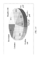
- FIG. 14 shows the weight distribution in a conventional lead-acid batteries used for traction.
- the subject matter described here can eliminate or greatly reduce the negative active mass, positive and negative grid, and top lead components, removing about half the lead found in a conventional lead-acid battery.
- the subject matter described has the potential to eliminate weight (around half in some examples) and can increase (doubling in some examples) the energy density.
- conventional lead-acid batteries can be low voltage, high current devices. These properties are a poor match to higher voltage systems used in vehicles and renewable energy systems.
- Efforts have been made to improve cycle life.
- One approach is to replace the negative active mass ("NAM”) with a carbon electrode. Hydrogen can intercalate in the carbon in a manner similar to lithium intercalation in a lithium-ion battery. This can reduce or eliminate shedding on that layer.
- Another approach can integrate a super-capacitor with a conventional battery to provide extended life for repeated power bursts needed for start-stop cycles.
- Bipolar lead-acid battery such as Blead-acid batteries, or bipolar batteries.
- Examples can include a series-connected stack of cells, operating at high voltage and low current. This configuration can reduce or eliminate heavy internal conductors used in low voltage, high current batteries, and can provide a high voltage output.
- Blead-acid batteries promises advantages such as high energy density by virtue of reduced conductor mass.
- several issues have limited commercialization. These include cell-to-cell leakage, layer degradation in a corrosive environment that includes both the sulfuric acid electrolyte and oxygen radicals formed during charging, active mass shedding, and electrode sagging that presents issues for layer separation.
- Ceramic conducting TiO 2 substrates can use ceramic conducting TiO 2 substrates.
- the active material is a paste as in conventional lead-acid batteries. Ceramic layers can be less susceptible to sagging, but may be hard to manufacture in high volume at low cost.
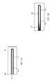
- FIG. 1A shows a schematic representation of a battery layer showing an aggregate of particles on a lead substrate, with arrows 110 indicating the flow of ions, according to an example.
- the pasted active mass layer 102 can include an aggregate of particles 104 disposed on a substrate 108, which can be a few microns in diameter. Electrolyte can flow through channels between the particles. The channel diameter can be a few microns and the length can be substantially similar to the thickness of the active mass, 1-3 millimeters in some examples.
- FIG. 1B shows a schematic representation of a simplified representation of the layer of FIG. 1A , according to an example.
- channels 106 can be theoretically modeled as straight channels.
- the electrolyte ions can diffuse the length of the channel with low, or even without, depletion, and the reaction can proceed along the full length of the channel 106.
- the electrolyte ions can be consumed before they can diffuse the full length of the channel 106.
- the active mass deep in the layer does not react as desired, and the available energy, which is associated with available reactions with the AM, can decrease.
- FIG. 2A shows a pore with low current density, according to an example.
- FIG. 2B shows a pore with high current density, according to an example.
- channel 206 which represent pores 208, have a lead sulfate coating 210.
- the current at onset of ion depletion scales as 1/L 2 , where L is the channel length.
- the narrowing 212 represents that more reactions have taken place than at less narrow portions.
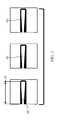
- FIG. 3 shows three layers with thinner active mass replacing a single layer, according to an example.
- One solution to the problem of unbalanced ion depletion is to split the active mass into several thinner layers, as shown in FIG. 3 , in which the length "L" shown in FIG. 2 has been reduced by a factor of 1/X to provide a shorter channel 302.
- more channels 302', 302" can be used. They may total X in number, but other numbers are possible.
- Such a configuration can retain the same amount of active mass, so the battery can retain the same or a similar capacity. Because of the shorter channels, the battery can run at higher current while accessing a greater portion of the active mass. For example, dividing a single 1 millimeters thick active mass layer into three 0.3 millimeters thick active mass layers provides 9 times more current without loss of capacity.
- New systems and methods described herein provide battery layers with thin active mass layers. These layers can be closely spaced, and the amount of active mass can remain constant to retain a desired battery capacity. Additionally, these thin active mass layers have other desirable attributes.
- a lead layer expands about 60% when converted to lead sulfate, and the lead oxide layer expands about 20%. This expansion can cause shedding of the active mass in deep cycling.
- a thinner layer has less mechanical stress at the interface, and is less likely to shed, allowing the battery to operate reliably in deep cycling.
- Examples disclosed herein provide a bipolar lead-acid battery with layers that can be much thinner than conventional plates, which can enable balanced ion depletion.
- Silicon wafers can be used as substrates and provide layers that are light, resistant to reaction with sulfuric acid, and that are inexpensive.
- Active mass layers can be formed using plating or electrophoretic deposition instead of pasting, enabling controlled formation of thin layers.
- the composition can be varied in depth to provide for selected critical properties such as porosity, grain size, and stress.
- Contact and barrier layers can be included.
- a sacrificial template process is described by way of example to provide controlled porosity, employing one or both of deposition of a sacrificial layer and co-deposition using electrophoresis.
- Methods to package the battery are also described, and can include sealing a stack of layers in a molded form, adding electrolyte, and affixing a cover.
- Examples provide a bipolar lead-acid battery design that enables the use of thin layers to provide a battery with an increased layer density over that of conventional batteries. Examples allow spreading the active mass over a large number of thin layers to reduce the effect of Puekert's Law, enabling deep cycling (i.e., balanced ion depletion) with reduced shedding of active mass. Examples provide a high voltage output suitable for electric vehicle and renewable energy systems. Examples use less (half in some examples) of the lead of conventional lead-acid batteries, which can increase (double in some examples) energy and power density.
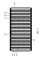
- FIG. 4 shows a stacked or bipolar battery configuration, including alternating plates and separators or spacers soaked with electrolyte, according to an example.
- a electrochemical battery has two terminals: a cathode (positive) and anode (negative). A reduction reaction occurs at the cathode and an oxidation reaction occurs at the anode.
- the battery potential is the sum of the half-reaction voltages. In the case of lead-acid, the positive plate is typically lead oxide, and the half-reaction voltage is about 1.6 volts. The negative plate is typically lead, and the half-reaction voltage is 0.4 volts.
- a battery cell includes, at a minimum of an anode and cathode. Voltages for cells wired in series are additive. Accordingly, 10 lead-acid cells connected in series can provide 20 volts (e.g., 10 cells x 2 volts/cell). In an example series connection, the string can include a series of anodes connected to cathodes, with the intervening electrolytes electrically isolated.
- the example includes a stack 400 of layers such as plates packaged with spacers.
- the stack 400 can include one or more anodes 410 separated from cathodes 412, such as by spacers or separator 408. Gaps between the plates can be filled with sulfuric acid electrolyte. The electrolyte masses or volumes can be electrically isolated so that the plates can be in series.
- the spacer material can be fiberglass, which is porous and can absorb sufficient sulfuric acid.
- the plate spacing can be 0.5 millimeters.
- Separators or spacers 408 can prevent shorting of the plates, and can be thin sheets of fiberglass. In some cases, the plates are stiff, and in some of those examples spacers are not necessarily used. Electrolyte, which can be sulfuric acid, can be disposed in a space between plates. Electrolyte can be soaked into the spacers.
- the stack can form a series-connected arrangement of cells.
- Voltage can be equal to (N-1)V Cell , where N is the number of plates (with one at each end for connection to the positive 404 and negative 402 terminals), and V Cell is the voltage of a single cell.
- N is the number of plates (with one at each end for connection to the positive 404 and negative 402 terminals)
- V Cell is the voltage of a single cell.
- the cell voltage for the lead-acid reaction can be around 2 volts.
- a battery having 101 plates can have a voltage of 200 volts.
- a housing 406 is shown, mechanically maintaining multiple cells in a stack.
- Examples can include electrically conducting substrates with an anode on one side and cathode on the other.
- the substrate can act as the conductor or "wire" to connect the cells together while isolating the electrolytes from one-another.
- Such examples can use bare silicon or carbon coated silicon as the counter electrode to the lead oxide electrode.
- the cathode can provide most of the cell voltage. Some cases omit lead as the material for the half cell reaction at the anode while providing a place for a reduction reaction to occur on that side of the cell.
- One way to accomplish this is to allow protons from the electrolyte solution to react (intercalate), as occurs in other types of batteries such as lithium ion. This reaction operates in both carbon and silicon.
- the cell voltage can be at least 1.6 volts (the cathode half-cell potential), but the mass and weight of the lead on the anode can be reduced or eliminated, resulting in an increase in power and energy density and reductions in cost and toxic material content. Life can also be extended because lead suffers the greatest expansion when it converts to lead sulfate, and therefore undergoes the greatest stress. The loss of voltage can easily be made up by adding more series-connected cells.
- An exposed leftmost electrode 402 can serve as a terminal, such as for coupling electrically and mechanically with electronics.
- the exposed major face of the rightmost terminal 404 can serve as an electrode of the opposite polarity, and can serves as a terminal as well.
- the stack is disposed in a housing or container and is connected to electronics outside the housing via one or more feedthroughs extending through the housing.
- the anode is shown having a plurality of protrusions 416 defining channels 418.
- the present subject matter is not so limited, and examples in which the cathode has protrusions are also contemplated, as are examples in which no protrusions are used.
- Such a battery can in some examples, use silicon wafers with standard solar cell texture.
- Some examples use textured silicon, such as cut wafers.
- As-cut silicon wafers originally used for solar cells, can be used as the substrates for the electrodes. These wafers are light (about a quarter the density of lead), can be resistant to sulfuric acid corrosion, and can be generally available at low cost by virtue of their high volume of use.
- As-cut wafers can have a surface roughness that provides good adhesion, such as for mechanically joining with a coating.
- multi-crystal (MC) wafers can be formed by iso-texturing, such as in a bath of hydrofluoric acid and nitric acid.
- Multi-crystalline wafers can provide a square form factor and lower cost.
- Single crystal wafers can also be used.
- Single crystals can have a pyramidal texture, typically formed with a potassium hydroxide ("KOH") /isopropyl alcohol etch. Because large grain size is not as important, MC wafers can be made more rapidly than they are for solar applications, which can provide for lower cost.
- KOH potassium hydroxide
- a lower cost metallurgical grade silicon can be used, as its purity is compatible with battery applications disclosed herein. Other silicon, such as electronic, solar or semiconductor grade can be used, but are generally more expensive.
- wafers can be doped.
- Doped wafers can have a resistivity typically less than 1 ⁇ -cm. In some examples, the resistivity can be less than 0.001 ⁇ -cm. Lower resistivity can improve efficiency as battery current flows through the wafers. Low resistivity can also improve the quality of contacts to the silicon. Dopants can be used, such as phosphorus, boron, antimony or arsenic. Such wafers can be less than 500 ⁇ m (0.5 millimeters) thick, and can be less than 200 ⁇ m thick.
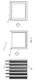
- Wafers can be square, with an edge length of 156 millimeters for standard solar cell wafers, although rectangular wafers, or wafers with other form factors such as clipped corners can also be used.
- Use of a standard edge length can enable the use of wafers manufactured in high volume, which can reduce cost, although other edge lengths can be used.
- Use of standard size wafers can allow for the use of standard manufacturing equipment to handle and process the wafers during battery manufacturing.
- active mass can be formed on one or both sides of a substrate.
- Lead can be plated onto both sides.
- One plated side can be masked and the other can be exposed to a sulfuric acid bath. While exposed, a current can be run through such a bath using a lead negative electrode.
- Such an approach can convert the exposed side to lead oxide using a process termed "forming."
- only one side of the silicon substrate is coated with lead and converted to lead oxide or, alternately, coated with lead oxide.
- the battery can have a lower voltage that an example with active material lead coated on both sides.
- the half-cell potential for lead oxide to lead sulfate reaction can be 1.68 volts.
- a battery with lead coated on only one side can use less (e.g., half) lead, so it can be less toxic and lighter in weight.
- lead can expand more than lead oxide when converted to lead sulfate, so plates without a lead coated side can experience less stress during cycling.
- either one or both sides can be coated with active mass.
- Other materials can be used as active mass and the use of the silicon plates is not exclusive to lead-acid type batteries.
- hydrogen can intercalate into the silicon on the opposite electrode, much as lithium does in a lithium-ion battery.
- a silicon surface can be coated with an inert material such as carbon, and hydrogen can intercalate into the carbon. Such intercalation can be beneficial, as it can help a cell resist bulging due to gas production.
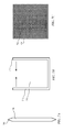
- FIG. 5 shows a method for assembling the stacked battery.
- a side view of battery plates and spacers alternately stacked is shown.
- alternating layers of plates 502 and fiberglass spacers 504 can be stacked, as shown in the left drawing in FIG. 5 .
- the battery stack can be placed in a U-shaped frame 506 that provides three sides.
- An adhesive that is resistant or impervious to sulfuric acid, such as epoxy or any of a number of plastics resistant to sulfuric acid, such as polypropylene, can be injected into the space 508 between the u-shaped frame 506 and the battery stack 500.
- electrolyte can be added and a cover 510 can be put in place.
- fiberglass spacers can resist or prevent adhesive from seeping into the space between the plates any more than a small region near the edges of the faces of the plates. It can be helpful to seal the edges 512 of the stack so that the electrolyte masses (i.e., volumes with electrodes of opposite polarity on opposing sides) can be electrically isolated.
- laser cut grooves can be formed near the periphery of the plates, using laser grooving equipment common in solar cell manufacturing. Such grooves can be 10-20 ⁇ m deep and on the order of 50 ⁇ m wide. This can provide a reentrant structure to improve the quality of the edge seal.
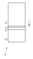
- FIG. 6 shows a method for assembling the stacked battery using removable spacers, according to an example.
- a battery stack can be made with spacers 602 that extend out of the stack on the top side, as shown in the side view on the left.
- the battery stack can be placed in a U-shaped frame 606, shown in front view in the center, that provides three sides.
- An adhesive that is resistant or impervious to sulfuric acid, such as epoxy or any of a number of plastics resistant to sulfuric acid, can be injected into the space between the U-shaped frame 606 and the battery stack 600.
- the spacers can be pulled out, electrolyte can be added, and a cover 610 can be put in place.
- the cover 610 can have a vent to prevent gas pressure build-up if the battery is overcharged, and can be removable to allow recharging of electrolyte.
- FIG. 7A shows a top view of a plate-shaped spacer including tapered edges, according to an example.
- the edges of the spacers can be tapered, as shown in FIG. 7A , which is a top view.
- the tapered edges 706 extending away from a main body 708 can reduce contact area between the spacer an another structure such as a frame, providing for easier removal. They also provide a tapered region that can be filled with the epoxy or plastic to provide an improved seal.
- FIG. 7B shows a front view of a U-shaped spacer, according to an example.
- spacers can be U-shaped, with a spacer portion 710 defining an inner void 712.
- Such a spacer can allow for removal by pinching the ends 714 in the direction of the arrows and lifting the spacer out of a frame, a process that can permit air to enter the frame to ease spacer removal.
- FIG. 7C shows a fiberglass spacer having an edge lining of a fiberglass spacers, according to an example.
- fiberglass separators can wick the glue so that it extends excessively into the space between the plates.
- Forming an edge liner 704 around the fiberglass spacers 702, as shown in FIG. 7C can prevent this.
- the fiberglass can be melted to form a glass frame that does not wick adhesive.
- adhesive or plastic can be applied to the rim of the spacers to form a frame consisting of set adhesive.
- the edge liner can be soft and flexible if an appropriate adhesive such as silicone is used.
- the spacers can be made of a non-stick material such as Teflon, or can have a Teflon coating to ease removal. They can also have holes through the top that can be aligned so that one or more rods can be passed through the set of spacers, simplifying alignment and removal.
- a mold release material can be applied to one or more surfaces to provide for easier removal.
- the edges of the silicon plates may have nicks or defects resulting during their manufacture. These nicks can cause the plates to break when handled.
- the plates can be coated with epoxy or plastic before assembly. This is called pre-coating. It can protect the edges, to reduce the risk of breaking wafers.
- the coating can be by dipping or direct application. In some examples, the coating thickness equals half the plate separation.
- the plates can be stacked and an additional layer of epoxy or plastic applied to form the outer housing of the battery.
- the pre-coating material can be a plastic substantially resistant to sulfuric acid. The sum of the thicknesses of the pre-coating on plate faces can be approximately equal a plate separation between plates.
- FIG. 8 shows a flow chart of a battery assembly process, according to an example. The process can be used to produce the examples discussed in FIGS. 4-6 and other disclosed herein.
- electrodes are placed into a stack.
- the electrode stack is placed in a frame.
- adhesive is added and, respectively, set to adhere the stack to the frame.
- an optional step allows for removal of at least some spacers.
- one or more interior space defined between electrodes adhered to the frame can be filled with electrolyte.
- a cover or top can be added to the frame to seal in the electrolyte.
- FIG. 9 is a cross-sectional view of a battery plate with an active mass coating showing different layers, from left to right showing silicon, nickel silicide, barrier layer, lead oxide, according to an example.
- FIG. 9 shows an example multiple layer stack.
- the figure shows a plate 900 comprising silicon 902, nickel silicide 904, a barrier layer 906 and lead oxide 908. It should be noted that it is often desirable to remove any native oxide from the silicon before applying a layer. This can be done with sandblasting or using a chemical etch such as buffered hydrofluoric acid.
- a silicide layer between the substrate and the active mass.
- Some examples interpose a nickel silicide layer between the substrate and the active mass.
- Such a layer can be formed using an electroless nickel deposition or a vacuum process such as evaporation or sputter deposition. Some examples include a heating cycle such as at 500°C. Some examples heat for around 10 seconds.
- a silicide layer can be formed on the opposite side to improve contact to the inert layer (e.g., carbon) or to the electrolyte.
- other silicides such as molybdenum, titanium, tungsten and their alloys can be used instead of or in addition to nickel.
- Additional layers can be added for protecting the silicon from reaction with the electrolyte and to improve adhesion of the active mass to the substrate.
- Such layers can include TiN, TaN, molybdenum selenide, tin or chrome, and can be formed on one or both sides of the substrate.
- Methods of deposition include, but are not limited to, sputtering, reactive sputtering or evaporation.
- Barrier or adhesion layers can be relatively thin, such as from 20 to 100 nm.
- FIG. 10 is a flow chart of the process for making the battery plate, including formation of a silicide contact and addition of layers to form a barrier to protect the plate from acid corrosion and to promote adhesion of the active mass, according to an example.
- the process can be used on one or both faces of a layer.
- the method starts by providing a silicon substrate.
- the substrate can be cleaned to remove contamination and organic deposits. Cleaning solutions that can be used include a mixture of sulfuric acid and hydrogen peroxide to remove organics.
- the surface can also be etched in hydrofluoric acid to remove any oxide layer that forms after the sulfuric/peroxide clean, or can be sandblasted.
- electroless nickel can be deposited.
- electroless nickel can be can be vacuum deposited as described above.
- the deposit can be baked. Such a deposit can be heated at 300-700°C, such as for 30 seconds to form a silicide contact layer.
- a barrier can be deposited. The barrier can be plated or sputtered, among other methods of forming.
- an adhesion and/or barrier layers can be deposited.
- the active mass can be formed using methods described herein.
- the active mass can be conditioned, for example, to turn it from lead to lead oxide. In some examples, lead can be plated directly to the silicon. The lead can optionally be heated at 200°C for 5 minutes to improve contact and adhesion.
- Examples can form an active mass with controlled porosity and pore size.
- the active mass can be plated.
- the active mass can be less than 1 millimeter thick. Some examples are from 0.2 to 0.3 millimeters thick.
- the active mass can include lead(IV) oxide, PbO 2 .
- the notation lead "(IV)" refers to lead with a valence of +4.
- a plated material can also include lead, which can be electrolytically converted to PbO 2 using forming or conditioning. In some conditioning processes, current can be run through the plate in a 6 molar sulfuric acid bath to convert it to lead sulfate. The current can be reversed to form lead oxide on a positive plate.
- FIGS. 11A-C show a pictorial representation of the process of making a porous active mass, according to an example.
- a deposition can be made porous using various methods.
- additives can be put in the plating solution, such as those used to make a matte finish plating.
- a sacrificial layer 1102 can be used.
- a mix of fine soluble particles 1104 and a matrix material 1106 such as a cured resin such as paraffin wax or a polymer such as etch-resist can be prepared.
- the particles 1104 can have the same size as the active mass grains, which can be around 5 ⁇ m diameter. They can be of a soluble material such as a crystalline salt, sodium chloride being one example.
- the mix can be applied to the substrate 1108, which can be heated to allow the matrix (e.g., paraffin) to flow.
- the mix 1102 can be allowed to solidify, by, for example, cooling or evaporation of organic constituents.
- the wafer can be placed in water so that the soluble particles 1104 dissolve. Such a process can produce a porous organic matrix 1106.
- the wafer can be placed in a plating bath.
- the active mass material can be plated into the pores.
- the matrix 1106 can be thicker than the plating 1110 thickness, which can be determined by the plating time and current.
- the matrix can be dissolved in a solvent to leave the porous active mass layer, which can be conditioned to form lead(IV) oxide if the original plating material was lead.
- electrophoretic deposition can be used to deposit the active mass.
- Electrophoresis is a process in which charged particles can be attracted to an electrode.
- a suspension of active mass particles can be made in an ethanol bath, such as by using ultrasonic agitation.
- ethanol and compositions thereof, is that it is a poor conductor of electricity, so a field can be established across the bath.
- a small amount of sulfuric acid can be added to the suspension, for example 0.5 milliliters per 100 milliliters of bath. Such an addition can provide a source of ions to charge suspended active mass particles.
- the electrode to be coated can be placed in the bath and connected to the negative terminal of a voltage source, such as a 50-200 volt source, with an electrode spacing on the order of 2-5 centimeters.
- a voltage source such as a 50-200 volt source
- the potential urges active mass particles to the surface, where they deposit.
- a coated plate can be baked at a temperature exceeding 100°C. Some examples are baked at 200°C for 30 minutes. Baking can drive ethanol out of the coating.
- Integrity refers to resistance to flaking or decomposition of the active mass layer.
- a soluble species such as salt grains can also be co-deposited, and can be dissolved as described above to control film porosity. This has the advantage of reducing or eliminating the need for sacrificial paraffin and subsequent plating steps.
- FIG. 12 is a flow chart for making a porous active mass, according to an example.
- the flowchart can be used to make the apparatus of FIG. 11 .
- a filled matrix can be applied to a substrate.
- filler in the matrix can be dissolved.
- the matrix can be plated.
- the matrix can be dissolved.
- the remaining material can be conditioned.
- FIG. 13 shows a micrograph 1300 of a paraffin matrix 1302 with holes 1304 left behind after salt crystals have been dissolved.
- the ratio of matrix material to particles can determine the porosity. Particle size and shape can determine the pore size.
- the mixture can contains 50-70% solids. A high solid fraction can encourage the formation of pores that are continuous, which enables thorough plating throughout the matrix. In some cases matrix material wets the top surface, in which can the surface can be lightly scraped to expose salt.
- the consistency of the active mass can be varied in depth. For example, multiple sequential depositions can be layered on top of one another. During a deposition, parameters can be altered, making it possible to vary parameters such as grain size, porosity, composition, or film stress.
- Example 1 can include or use subject matter (such as an apparatus, a method, a means for performing acts, or a device readable medium including instructions that, when performed by the device, can cause the device to perform acts), such as a stack of electrodes, including: a first electrode including a silicon substrate and an active material or active mass disposed on the silicon substrate, a second electrode disposed in the stack in alignment with the first electrode, and a separator disposed between the first electrode and the second electrode.
- subject matter such as an apparatus, a method, a means for performing acts, or a device readable medium including instructions that, when performed by the device, can cause the device to perform acts
- a stack of electrodes including: a first electrode including a silicon substrate and an active material or active mass disposed on the silicon substrate, a second electrode disposed in the stack in alignment with the first electrode, and a separator disposed between the first electrode and the second electrode.
- the example can include a housing, with the stack of electrodes disposed in the housing, electrolyte filling the housing and in contact with the first electrode and the second electrode, a seal coupled between the housing and the stack to define an interior space extending between the first electrode and the second electrode, the seal adapted to resist the flow of electrolyte from the interior space, a cover coupled to the housing, and a cover seal adapted to resist the flow of the electrolyte from inside the interior space.
- Example 2 can optionally can optionally include the subject matter of any of the preceding examples 1, wherein a major face of the first electrode is exposed to an exterior, the second electrode is of a different polarity, and a second major face of the second electrode is exposed to an exterior, opposite the first major face.
- Example 3 can optionally include the subject matter of any of the preceding examples, wherein the active material includes lead (or a lead compound) and the electrolyte includes sulfuric acid.
- Example 4 can optionally include the subject matter of any of the preceding examples in which at least one intervening layer is disposed between the substrate and the active material.
- Example 5 can optionally include the subject matter of any of the preceding examples wherein the intervening layer is formed of at least one of a group including TiN, TaN, molybdenum selenide, tin and chrome.
- Example 6 can optionally include the subject matter of any of the preceding examples wherein the intervening layer includes a silicide.
- Example 7 can optionally include the subject matter of any of the preceding examples wherein the silicide includes tungsten, titanium, nickel or molybdenum.
- Example 8 can optionally include the subject matter of any of the preceding examples, wherein the substrate is less than 0.5 millimeters thick and the active material is less than 0.5 millimeters thick.
- Example 9 can optionally include the subject matter of any of the preceding examples, wherein the substrate has a cut surface onto which the active material is disposed.
- Example 10 can optionally include the subject matter of any of the preceding examples, wherein the active material is porous.
- Example 11 can optionally include the subject matter of any of the preceding examples, wherein a major face of the substrate has a rectangular perimeter, with side lengths of approximately 156 millimeters.
- Example 12 can optionally include the subject matter of any of the preceding examples, including forming a battery electrode by disposing an active material coating onto a silicon substrate, assembling the battery electrode into a stack of battery electrodes, the battery electrode separated from other battery electrodes by a separator, disposing the stack in a housing, filling the interior space with electrolyte, and sealing the housing to resist the flow of electrolyte from the interior space.
- Example 13 can optionally include the subject matter of any of the preceding examples in which the plated coating is lead, and further including oxidizing the coating after application to form lead(IV) oxide.
- Example 14 can optionally include the subject matter of any of the preceding examples, including forming a silicide between the substrate and the active material by disposing a nickel onto the substrate and heating the substrate.
- Example 15 can optionally include the subject matter of any of the preceding examples wherein disposing the nickel includes plating the nickel including applying the nickel using electroless deposition.
- Example 16 can optionally include the subject matter of any of the preceding examples in which the silicide is formed by sputtering or evaporating a metal and heating the substrate.
- Example 17 can optionally include the subject matter of any of the preceding examples, wherein the active material is a porous plated active material formed by: disposing a sacrificial layer of matrix material and particles onto the substrate, dissolving the particles to form a matrix with pores, plating active material into at least some pores, and dissolving the matrix.
- the active material is a porous plated active material formed by: disposing a sacrificial layer of matrix material and particles onto the substrate, dissolving the particles to form a matrix with pores, plating active material into at least some pores, and dissolving the matrix.
- Example 18 can optionally include the subject matter of any of the preceding examples, wherein disposing the active material onto the substrate includes applying the substrate using electrophoresis.
- Example 19 can optionally include the subject matter of any of the preceding examples, including mechanically fixing the stack to the housing to define an interior space, with the separator disposed in the interior space, and removing the separator.
- Example 20 can optionally include the subject matter of any of the preceding examples, wherein disposing the active material includes electrophoretic co-deposition of the active material along with a sacrificial material, and defining a porous active material by dissolving the sacrificial material after electrophoretic co-deposition.
- Example 21 can optionally include the subject matter of any of the preceding examples, in which the silicon substrate is highly doped.
- Example 22 can optionally include the subject matter of any of the preceding examples in which the silicon resistivity is less than 1 ⁇ -cm.
- Example 23 can optionally include the subject matter of any of the preceding examples which the substrate has an as-cut surface.
- Example 24 can optionally include the subject matter of any of the preceding examples which the silicon has a standard solar cell texture.
- Example 25 can optionally include the subject matter of any of the preceding examples which the silicon is metallurgical grade material.
- Example 26 can optionally include the subject matter of any of the preceding examples which the substrate is multi-crystal silicon.
- Example 27 can optionally include the subject matter of any of the preceding examples including a process for applying an active mass coating to a silicon battery plate in which the coating is plated or deposited using electrophoresis.
- Example 28 can optionally include the subject matter of any of the preceding examples in which the plated or electrophoresis deposited coating is less than 1 millimeters thick.
- Example 29 can optionally include the subject matter of any of the preceding examples, including intervening layers between the silicon substrate and active mass to promote adhesion of the active mass to the battery plate.
- Example 30 can optionally include the subject matter of any of the preceding examples in which an additive is included in the plating solution to promote porosity.
- Example 31 can optionally include the subject matter of any of the preceding examples in which a sacrificial layer is applied to the battery plate, said sacrificial layer consisting of a matrix material and particles, said particles being subsequently dissolved to form a matrix with pores, at least a portion of said pores being then filled by plating and said matrix being subsequently dissolved, in which the matrix material is at least one of wax and a polymer.
- Example 32 can optionally include the subject matter of any of the preceding examples in which said particles are a crystalline salt.
- Example 33 can optionally include the subject matter of any of the preceding examples in which the crystalline salt is sodium chloride.
- Example 34 can optionally include the subject matter of any of the preceding examples that also includes porous spacers between plates.
- Example 35 can optionally include the subject matter of any of the preceding examples in which the porous spacer material includes fiberglass.
- Example 36 can optionally include the subject matter of any of the preceding examples in which a stack is formed including alternating battery plates, porous spacers, and removable spacers, said stack is then placed in a containment fixture, sealant is applied to the periphery of said stack, and said removable spacers are removed after said sealant sets.
- Example 37 can optionally include the subject matter of any of the preceding examples in which three sides are sealed, the spacers removed, electrolyte added, and a top cover placed on the battery.
- Example 38 can optionally include the subject matter of any of the preceding examples in which one or more edges of the removable spacers are tapered.
- Example 39 can optionally include the subject matter of any of the preceding examples in which a release coating is applied to the removable spacers.
- Example 40 can optionally include the subject matter of any of the preceding examples in which the removable spacers have a U-shape so that removal includes a step of pinching the ends of the U-shape toward each other.
- Example 41 can optionally include the subject matter of any of the preceding examples in which the removable spacers are reusable.
- Example 42 can optionally include the subject matter of any of the preceding examples in which a stack is formed including alternating battery plates and porous spacers, said stack is then placed in a containment fixture and sealant is applied to the periphery of said stack.
- Example 43 can optionally include the subject matter of any of the preceding examples in which three sides are sealed, electrolyte added, and a top cover placed on the battery.
- Example 44 can optionally include the subject matter of any of the preceding examples in which the porous spacers have edge liners to prevent absorption of the sealant into the spacers.
- Example 45 can optionally include the subject matter of any of the preceding examples in which the edge liner is an adhesive.
- Example 46 can optionally include the subject matter of any of the preceding examples in which the adhesive is silicone.
- Example 47 can optionally include the subject matter of any of the preceding examples in which the edge liner is formed by melting the edge of the fiberglass spacer.
- Example 48 can optionally include the subject matter of any of the preceding examples in which one face of the substrate is inert.
- Example 49 can optionally include the subject matter of any of the preceding examples in which the inert face is silicon
- Example 50 can optionally include the subject matter of any of the preceding examples in which the inert face is coated with carbon.
- Example 51 can optionally include the subject matter of any of the preceding examples in which the inert face is a silicide.
- Example 52 can optionally include the subject matter of any of the preceding examples in which the active mass on at least one side is applied using electrophoresis.
- Example 53 can optionally include the subject matter of any of the preceding examples in which the active mass material includes lead oxide.
- Example 54 can optionally include the subject matter of any of the preceding examples in which active mass is baked at a temperature exceeding 100°C after electrophoretic deposition.
- Example 55 can optionally include the subject matter of any of the preceding examples in which an intervening layer is disposed between the electrophoretic active mass deposition and the plate substrate.
- Example 56 can optionally include the subject matter of any of the preceding examples in which plate material includes silicon.
- Example 57 can optionally include the subject matter of any of the preceding examples, in which an electrode is formed by electrophoretic co-deposition of an active mass material and a sacrificial material, said sacrificial material being dissolved after electrophoretic co-deposition in order to increase the porosity of the active mass layer.
- Example 58 can optionally include the subject matter of any of the preceding examples active mass layer in which the active mass is co-deposited with a second material, a function of said second material being to improve a physical property of the active mass layer.
- Example 59 can optionally include the subject matter of any of the preceding examples in which the physical property is adhesion.
- Example 60 can optionally include the subject matter of any of the preceding examples in which the physical property is integrity of the active mass layer.
- Example 61 can optionally include the subject matter of any of the preceding examples including sand blasting the plate surface.
- Example 62 can optionally include the subject matter of any of the preceding examples in which a battery uses a plurality of plates, with at least two plate shaving edges being pre-coated.
- Example 63 can optionally include the subject matter of any of the preceding examples in which the pre-coating material is epoxy.
- Example 64 can optionally include the subject matter of any of the preceding examples in which the pre-coating material is a plastic substantially resistant to sulfuric acid.
- Example 65 can optionally include the subject matter of any of the preceding examples in which the sum of the thicknesses of the pre-coating on plate faces approximately equals the plate separation.
- Example 66 can optionally include the subject matter of any of the preceding examples in which a stack of plates is sealed after stacking to provide an outer housing for the battery.
- Example 67 can optionally include the subject matter of any of the preceding examples in which the sealing material is plastic.
- Example 68 can optionally include the subject matter of any of the preceding examples in which the sealing material is epoxy.
- Example 69 can optionally include the subject matter of any of the preceding examples in which the active mass consistency is varied with depth through the use of either multiple sequential depositions or varying deposition parameters through the deposition process.
- Example 70 can include, or can optionally be combined with any portion or combination of any portions of any one or more of Examples 1-69 to include subject matter that can include means for performing any one or more of the functions of Examples 1-69, or a machine-readable medium including instructions that, when performed by a machine, cause the machine to perform any one or more of the functions of Examples 1-69.
- Method examples described herein can be machine or computer-implemented at least in part. Some examples can include a computer-readable medium or machine-readable medium encoded with instructions operable to configure an electronic device to perform methods as described in the above examples.
- An implementation of such methods can include code, such as microcode, assembly language code, a higher-level language code, or the like. Such code can include computer readable instructions for performing various methods. The code can form portions of computer program products. Further, in certain examples, the code can be tangibly stored on one or more volatile, non-transitory, or non-volatile tangible computer-readable media, such as during execution or at other times.
- Examples of these tangible computer-readable media can include, but are not limited to, hard disks, removable magnetic disks, removable optical disks (e.g., compact disks and digital video disks), magnetic cassettes, memory cards or sticks, random access memories (RAMs), read only memories (ROMs), and the like.
Landscapes
- Chemical & Material Sciences (AREA)
- General Chemical & Material Sciences (AREA)
- Chemical Kinetics & Catalysis (AREA)
- Electrochemistry (AREA)
- Engineering & Computer Science (AREA)
- Manufacturing & Machinery (AREA)
- Inorganic Chemistry (AREA)
- Composite Materials (AREA)
- Materials Engineering (AREA)
- Health & Medical Sciences (AREA)
- Life Sciences & Earth Sciences (AREA)
- Dispersion Chemistry (AREA)
- Molecular Biology (AREA)
- Ceramic Engineering (AREA)
- Battery Electrode And Active Subsutance (AREA)
- Cell Electrode Carriers And Collectors (AREA)
- Secondary Cells (AREA)
Claims (14)
- Batterie comprenant :un empilement (400) d'électrodes de batterie, comprenant :une tranche de batterie bipolaire (408) comprenant :une tranche conductrice de silicium (108) ;un matériau actif disposé sur au moins une face de la tranche de silicium pour former une première électrode de batterie (410) ; etune deuxième électrode de batterie (412) placée sur une face de la tranche conductrice de silicium à l'opposé de la première électrode ; etune troisième électrode de batterie disposée dans l'empilement avec la deuxième électrode, dont elle est physiquement espacée ;un boîtier (406), l'empilement d'électrodes de batterie étant disposé dans le boîtier ; etun électrolyte disposé dans le boîtier de sorte qu'une partie de l'électrolyte en contact avec la deuxième et la troisième électrodes de batterie est au moins partiellement isolée de la première électrode de batterie par la tranche conductrice de silicium,dans laquelle un empilement d'électrodes de batterie est configuré de manière à établir un chemin de conduction entre les première et deuxième électrodes de batterie à travers la tranche conductrice de silicium,caractérisée en ce qu'elle comprend un siliciure (904) sur au moins une face de la tranche conductrice de silicium entre le matériau actif et la tranche conductrice de silicium.
- Batterie selon la revendication 1, dans laquelle au moins une couche barrière (906) est disposée entre le siliciure (904) et le matériau actif (908).
- Batterie selon la revendication 2, dans laquelle la couche barrière (906) est formée d'au moins un élément du groupe comprenant le TiN, le TaN, le séléniure de molybdène, l'étain et le chrome ; et dans laquelle le siliciure (904) contient du tungstène, du titane, du nickel ou du molybdène.
- Batterie selon l'une quelconque des revendications précédentes, comprenant en outre :un joint couplé entre le boîtier (406) et l'empilement pour définir un espace intérieur s'étendant entre la deuxième électrode de batterie et la troisième électrode de batterie, le joint étant adapté à empêcher un écoulement d'électrolyte en provenance de l'espace intérieur ;un couvercle (510, 610) couplé au boîtier ; etun joint de couvercle entre le couvercle et le boîtier, le joint de couvercle étant adapté pour empêcher l'écoulement d'électrolyte en provenance de l'espace intérieur.
- Batterie selon l'une quelconque des revendications précédentes, dans laquelle le matériau actif contient du plomb, l'électrolyte contient de l'acide sulfurique, la tranche de silicium est formée de tranches de silicium de qualité métallurgique présentant une résistivité inférieure ou égale à 1 Ω-centimètre.
- Batterie selon l'une quelconque des revendications précédentes, dans laquelle la tranche présente une face découpée sur laquelle est disposé le matériau actif et le matériau actif est poreux.
- Procédé consistant à :former (1014) une plaque de batterie bipolaire (408) en disposant un revêtement de matériau actif sur au moins une face d'une tranche conductrice de silicium pour former une première électrode de batterie (410) ;former une deuxième électrode de batterie (412) située sur une face de la tranche conductrice de silicium à l'opposé de la première électrode de batterie ;assembler (802) la plaque de batterie sur un empilement (400) d'électrodes de batterie, la première électrode de batterie étant séparée d'une troisième électrode de batterie par un séparateur pour définir un espace intérieur entre la première électrode de batterie et la troisième électrode de batterie ;disposer (804) l'empilement dans un boîtier (406) ;remplir (812) d'électrolyte l'espace intérieur ; etsceller (806) le boîtier pour empêcher un écoulement d'électrolyte en provenance de l'espace intérieur,dans lequel l'empilement d'électrodes de batterie est configuré de manière à établir un chemin de conduction à travers la tranche conductrice de silicium,caractérisé en ce qu'un siliciure (904) est formé entre la tranche conductrice et le revêtement de matériau actif.
- Procédé selon la revendication 7 dans lequel le revêtement est en outre oxydé après avoir été appliqué, de manière à former de l'oxyde de plomb (IV).
- Procédé selon l'une quelconque des revendications 7 ou 8, consistant à former le siliciure (904) entre la tranche conductrice et le revêtement de matériau actif en disposant du nickel (1006) sur la tranche conductrice de silicium et en chauffant la tranche conductrice de silicium.
- Procédé selon la revendication 9, dans lequel l'étape consistant à disposer le nickel sur la tranche conductrice de silicium comprend le dépôt (1006) de nickel par une technique de dépôt autocatalytique.
- Procédé selon l'une quelconque des revendications 7 ou 8, consistant à former le siliciure (904) entre la tranche conductrice de silicium et le revêtement de matériau actif par pulvérisation ou évaporation d'un métal, puis à chauffer la tranche conductrice de silicium.
- Procédé selon l'une quelconque des revendications 7 à 11, dans lequel le matériau actif est un matériau actif poreux plaqué formé en :disposant (1202) une couche sacrificielle de matériau matriciel et de particules sur la tranche conductrice de silicium,dissolvant (1204) les particules pour former une matrice avec des pores ;plaquant (1206) le matériau actif au moins dans certains pores ; eten dissolvant (1208) la matrice.
- Procédé selon l'une quelconque des revendications 7 à 11, consistant à disposer le revêtement de matériau actif et un matériau sacrificiel sur la tranche conductrice de silicium par co-dépôt par électrophorèse ; et à dissoudre le matériau sacrificiel après le co-dépôt par électrophorèse.
- Procédé selon l'une quelconque des revendications 7 à 13, consistant à fixer mécaniquement l'empilement sur le boîtier pour définir l'espace intérieur, le séparateur étant disposé dans l'espace intérieur, et à supprimer le séparateur.
Priority Applications (4)
| Application Number | Priority Date | Filing Date | Title |
|---|---|---|---|
| EP15198173.5A EP3032610B1 (fr) | 2011-05-11 | 2012-05-11 | Batterie améliorée et procédé d'assemblage |
| DK15198173.5T DK3032610T3 (en) | 2011-05-11 | 2012-05-11 | AN IMPROVED BATTERY AND COLLECTION PROCEDURE |
| PL12722634T PL2668683T3 (pl) | 2011-05-11 | 2012-05-11 | Udoskonalony akumulator i sposób montażu akumulatora |
| SI201230476A SI2668683T1 (sl) | 2011-05-11 | 2012-05-11 | Izboljšan akumulator in metoda za sestavo |
Applications Claiming Priority (3)
| Application Number | Priority Date | Filing Date | Title |
|---|---|---|---|
| US201161484854P | 2011-05-11 | 2011-05-11 | |
| US201161525068P | 2011-08-18 | 2011-08-18 | |
| PCT/US2012/037598 WO2012155082A1 (fr) | 2011-05-11 | 2012-05-11 | Batterie améliorée et procédé d'assemblage |
Related Child Applications (1)
| Application Number | Title | Priority Date | Filing Date |
|---|---|---|---|
| EP15198173.5A Division EP3032610B1 (fr) | 2011-05-11 | 2012-05-11 | Batterie améliorée et procédé d'assemblage |
Publications (2)
| Publication Number | Publication Date |
|---|---|
| EP2668683A1 EP2668683A1 (fr) | 2013-12-04 |
| EP2668683B1 true EP2668683B1 (fr) | 2015-12-09 |
Family
ID=46147081
Family Applications (2)
| Application Number | Title | Priority Date | Filing Date |
|---|---|---|---|
| EP12722634.8A Active EP2668683B1 (fr) | 2011-05-11 | 2012-05-11 | Batterie améliorée et procédé d'assemblage |
| EP15198173.5A Active EP3032610B1 (fr) | 2011-05-11 | 2012-05-11 | Batterie améliorée et procédé d'assemblage |
Family Applications After (1)
| Application Number | Title | Priority Date | Filing Date |
|---|---|---|---|
| EP15198173.5A Active EP3032610B1 (fr) | 2011-05-11 | 2012-05-11 | Batterie améliorée et procédé d'assemblage |
Country Status (11)
| Country | Link |
|---|---|
| US (3) | US8828582B2 (fr) |
| EP (2) | EP2668683B1 (fr) |
| JP (2) | JP5634623B2 (fr) |
| KR (2) | KR101702414B1 (fr) |
| CN (2) | CN105958003B (fr) |
| CA (2) | CA2825921C (fr) |
| DK (2) | DK2668683T3 (fr) |
| ES (1) | ES2564364T3 (fr) |
| PL (1) | PL2668683T3 (fr) |
| SI (2) | SI3032610T1 (fr) |
| WO (1) | WO2012155082A1 (fr) |
Families Citing this family (18)
| Publication number | Priority date | Publication date | Assignee | Title |
|---|---|---|---|---|
| US10008713B2 (en) | 2011-05-11 | 2018-06-26 | Gridtential Energy, Inc. | Current collector for lead acid battery |
| WO2015127081A1 (fr) * | 2014-02-19 | 2015-08-27 | Gridtential Energy, Inc. | Collecteur de courant pour une batterie plomb-acide |
| US10090515B2 (en) | 2011-05-11 | 2018-10-02 | Gridtential Energy, Inc. | Bipolar hybrid energy storage device |
| SI3032610T1 (sl) | 2011-05-11 | 2019-04-30 | Gridtential Energy, Inc. | Izboljšana baterija in metoda za sestavljanje |
| US9812713B2 (en) * | 2013-05-23 | 2017-11-07 | Gridtential Energy, Inc. | Rechargeable battery with wafer current collector and assembly method |
| WO2015103285A1 (fr) * | 2013-12-30 | 2015-07-09 | Gridtential Energy, Inc. | Matériaux actifs architecturaux pour batteries d'accumulateurs au plomb |
| WO2015103295A1 (fr) * | 2013-12-30 | 2015-07-09 | Moomaw Daniel | Ensemble batterie bipolaire étanche |
| WO2015123343A1 (fr) * | 2014-02-11 | 2015-08-20 | Jaime Navarrete | Collecteur de courant au silicium pour batterie plomb-acide |
| JP6410127B2 (ja) * | 2014-03-11 | 2018-10-24 | 住友電気工業株式会社 | 電解液循環型電池、熱交換器、及び配管 |
| WO2015164848A1 (fr) | 2014-04-25 | 2015-10-29 | South Dakota Board Of Regents | Électrodes à haute capacité |
| EP3323169A4 (fr) * | 2015-07-15 | 2019-02-20 | Gridtential Energy, Inc. | Joint d'étanchéité de batterie bipolaire et agencements de nervure thermique |
| US9923189B2 (en) * | 2016-02-02 | 2018-03-20 | GM Global Technology Operations LLC | Electrophoretic deposition of an electrode for a lithium-based battery |
| EP3553871A4 (fr) * | 2016-12-07 | 2020-01-15 | Hitachi Chemical Company, Ltd. | Batterie de stockage au plomb de type liquide et son procédé de production |
| US10468674B2 (en) | 2018-01-09 | 2019-11-05 | South Dakota Board Of Regents | Layered high capacity electrodes |
| CN109818085A (zh) * | 2019-01-28 | 2019-05-28 | 肇庆理士电源技术有限公司 | 一种铅硅复合双极性电池 |
| CN116157545A (zh) * | 2020-08-05 | 2023-05-23 | 古河电气工业株式会社 | 铅合金、铅蓄电池用正极、铅蓄电池以及蓄电系统 |
| CN116034175B (zh) * | 2020-08-05 | 2024-04-12 | 古河电气工业株式会社 | 铅合金、铅蓄电池用正极、铅蓄电池、以及蓄电系统 |
| EP3993101A1 (fr) | 2020-10-28 | 2022-05-04 | Indian Oil Corporation Limited | Batterie plomb-acide à grille d'électrodes unique, son procédé de fabrication et ses performances |
Citations (3)
| Publication number | Priority date | Publication date | Assignee | Title |
|---|---|---|---|---|
| US20070139001A1 (en) * | 2003-10-06 | 2007-06-21 | Robert Hahn | Battery, especially a microbattery, and the production thereof using wafer-level technology |
| JP2007335206A (ja) * | 2006-06-14 | 2007-12-27 | Nissan Motor Co Ltd | 双極型電池 |
| US20100330411A1 (en) * | 2009-06-30 | 2010-12-30 | Sang Cheol Nam | Thin film battery and method of connecting electrode terminal of thin film battery |
Family Cites Families (49)
| Publication number | Priority date | Publication date | Assignee | Title |
|---|---|---|---|---|
| GB1394694A (en) | 1971-10-28 | 1975-05-21 | Montedison Spa | Lead acid accumulator or storage battery with supporting and/or connecting parts made of lihgt alloys |
| US3982960A (en) * | 1973-09-19 | 1976-09-28 | Ppg Industries, Inc. | Secondary electrochemical cell having non-consumable silicon cathode |
| US4324848A (en) * | 1981-01-26 | 1982-04-13 | General Electric Company | Positive electrode for lead acid battery |
| JPS60101867A (ja) * | 1983-11-08 | 1985-06-05 | Matsushita Electric Ind Co Ltd | 鉛蓄電池用極板及びその製造方法 |
| JPS61283173A (ja) | 1985-06-10 | 1986-12-13 | Sharp Corp | 電源素子 |
| US4828939A (en) | 1987-06-01 | 1989-05-09 | Eltech Systems Corporation | Bipolar metal/air battery |
| US5156932A (en) | 1991-05-02 | 1992-10-20 | Globe-Union, Inc. | Simple optimized lead-acid battery |
| JPH05135761A (ja) * | 1991-11-15 | 1993-06-01 | Matsushita Electric Ind Co Ltd | 鉛蓄電池 |
| JP2967635B2 (ja) * | 1991-12-13 | 1999-10-25 | 株式会社明電舎 | 金属ハロゲン電池の運転方法 |
| US5298683A (en) | 1992-01-07 | 1994-03-29 | Pacific Coast Technologies | Dissimilar metal connectors |
| US5279909A (en) | 1992-05-01 | 1994-01-18 | General Atomics | Compact multilayer ceramic-to-metal seal structure |
| US5429643A (en) | 1993-06-02 | 1995-07-04 | Gnb Battery Technologies Inc. | Method of assembling a bipolar lead-acid battery and the resulting bipolar battery |
| JP3254066B2 (ja) * | 1993-11-18 | 2002-02-04 | 科学技術振興事業団 | 非水又は固体電解質二次電池 |
| US5916709A (en) | 1993-12-03 | 1999-06-29 | Bipolar Power Corporation | Bipolar lead-acid battery |
| US5595839A (en) * | 1994-10-13 | 1997-01-21 | Yardney Technical Products, Inc. | Bipolar lithium-ion rechargeable battery |
| JPH08241707A (ja) | 1995-03-06 | 1996-09-17 | Res Dev Corp Of Japan | 酸化物薄膜を負極活性物質として使用した二次電池 |
| JPH09205152A (ja) | 1996-01-25 | 1997-08-05 | Sony Corp | 2層ゲート電極構造を有するcmos半導体装置及びその製造方法 |
| WO1998040920A2 (fr) | 1997-03-12 | 1998-09-17 | Nederlandse Organisatie Voor Toegepast-Natuurwetenschappelijk Onderzoek Tno | Procede pour fabriquer une plaque bipolaire |
| US5948562A (en) | 1997-11-03 | 1999-09-07 | Motorola, Inc. | Energy storage device |
| US6210827B1 (en) | 1998-03-06 | 2001-04-03 | Rayovac Corporation | Elongate air depolarized electrochemical cells |
| GB2387960B (en) | 2002-04-20 | 2004-06-09 | Hawker Batteries Ltd | Improvements in or relating to batteries |
| JP3935067B2 (ja) * | 2002-12-26 | 2007-06-20 | ソニー株式会社 | 二次電池用負極およびそれを用いた二次電池 |
| JP4573594B2 (ja) | 2004-07-27 | 2010-11-04 | 株式会社神戸製鋼所 | 二次電池 |
| JP2008541353A (ja) | 2005-05-03 | 2008-11-20 | ランディー オッグ, | バイポーラ電気化学二次電池 |
| US7829215B2 (en) * | 2005-08-29 | 2010-11-09 | University Of South Florida | Surface micromachined electrolyte-cavities for use in micro-aluminum galvanic cells |
| US20070269718A1 (en) * | 2006-05-22 | 2007-11-22 | 3M Innovative Properties Company | Electrode composition, method of making the same, and lithium ion battery including the same |
| US8097385B2 (en) | 2006-06-12 | 2012-01-17 | University Of Connecticut | Bipolar plate for fuel cell |
| JP2007335198A (ja) * | 2006-06-14 | 2007-12-27 | Matsushita Electric Ind Co Ltd | 非水電解質二次電池用複合活物質とそれを用いた非水電解質二次電池 |
| US7479466B2 (en) | 2006-07-14 | 2009-01-20 | Taiwan Semiconductor Manufacturing Co., Ltd. | Method of heating semiconductor wafer to improve wafer flatness |
| JP5135761B2 (ja) | 2006-10-25 | 2013-02-06 | 株式会社竹屋 | 遊技機 |
| EP2092586A1 (fr) * | 2006-11-15 | 2009-08-26 | Luminous Power Technologies Pvt Ltd | Batterie bipolaire |
| JP2008269972A (ja) | 2007-04-20 | 2008-11-06 | Nissan Motor Co Ltd | 非水溶媒二次電池 |
| KR100878718B1 (ko) * | 2007-08-28 | 2009-01-14 | 한국과학기술연구원 | 리튬이차전지용 실리콘 박막 음극, 이의 제조방법 및 이를포함하는 리튬이차전지 |
| JP5552731B2 (ja) | 2007-10-25 | 2014-07-16 | 日産自動車株式会社 | 双極型電池の製造方法、および双極型電池 |
| KR100972780B1 (ko) * | 2008-02-28 | 2010-07-29 | 주식회사 티지솔라 | 태양전지 및 그 제조방법 |
| US8633373B2 (en) | 2008-05-12 | 2014-01-21 | Mtpv Power Corporation | Sub-micrometer gap thermophotovoltaic structure (MTPV) and fabrication method therefor |
| US20110014520A1 (en) | 2008-07-25 | 2011-01-20 | Tomohiro Ueda | Bipolar battery |
| US8274756B2 (en) | 2009-12-15 | 2012-09-25 | HGST Netherlands B.V. | Use of carbon nanotubes to form conductive gaskets deployed in sensitive environments |
| EP2543098B1 (fr) * | 2010-03-03 | 2019-07-31 | Amprius, Inc. | Modèle de structures d'électrode pour le dépôt de matériaux actifs |
| BR112012022245A2 (pt) | 2010-03-05 | 2016-10-25 | Aic Blab Company | baterias de chumbo ácido reguladas por válvula bipolar leve e métodos para as mesmas |
| US9136544B2 (en) | 2010-03-11 | 2015-09-15 | Harris Corporation | Dual layer solid state batteries |
| US20130026409A1 (en) | 2011-04-08 | 2013-01-31 | Recapping, Inc. | Composite ionic conducting electrolytes |
| US10090515B2 (en) | 2011-05-11 | 2018-10-02 | Gridtential Energy, Inc. | Bipolar hybrid energy storage device |
| WO2015127081A1 (fr) | 2014-02-19 | 2015-08-27 | Gridtential Energy, Inc. | Collecteur de courant pour une batterie plomb-acide |
| SI3032610T1 (sl) | 2011-05-11 | 2019-04-30 | Gridtential Energy, Inc. | Izboljšana baterija in metoda za sestavljanje |
| US10008713B2 (en) | 2011-05-11 | 2018-06-26 | Gridtential Energy, Inc. | Current collector for lead acid battery |
| KR101250230B1 (ko) | 2011-07-21 | 2013-04-03 | 주식회사 모비솔루션 | 자릿값 기반의 투채널 인증 시스템 및 방법 |
| US9634319B2 (en) | 2011-09-09 | 2017-04-25 | East Penn Manufacturing Co., Inc. | Bipolar battery and plate |
| WO2015103295A1 (fr) | 2013-12-30 | 2015-07-09 | Moomaw Daniel | Ensemble batterie bipolaire étanche |
-
2012
- 2012-05-11 SI SI201231521T patent/SI3032610T1/sl unknown
- 2012-05-11 EP EP12722634.8A patent/EP2668683B1/fr active Active
- 2012-05-11 DK DK12722634.8T patent/DK2668683T3/en active
- 2012-05-11 JP JP2013552743A patent/JP5634623B2/ja active Active
- 2012-05-11 ES ES12722634.8T patent/ES2564364T3/es active Active
- 2012-05-11 US US13/994,434 patent/US8828582B2/en active Active
- 2012-05-11 CN CN201610407652.6A patent/CN105958003B/zh active Active
- 2012-05-11 WO PCT/US2012/037598 patent/WO2012155082A1/fr active Application Filing
- 2012-05-11 CN CN201280009851.1A patent/CN103493250B/zh active Active
- 2012-05-11 DK DK15198173.5T patent/DK3032610T3/en active
- 2012-05-11 PL PL12722634T patent/PL2668683T3/pl unknown
- 2012-05-11 KR KR1020167002096A patent/KR101702414B1/ko active IP Right Grant
- 2012-05-11 SI SI201230476A patent/SI2668683T1/sl unknown
- 2012-05-11 CA CA2825921A patent/CA2825921C/fr active Active
- 2012-05-11 CA CA2948737A patent/CA2948737C/fr active Active
- 2012-05-11 EP EP15198173.5A patent/EP3032610B1/fr active Active
- 2012-05-11 KR KR1020137021903A patent/KR101590529B1/ko active Application Filing
-
2014
- 2014-09-04 US US14/477,312 patent/US9570737B2/en active Active
- 2014-10-14 JP JP2014209992A patent/JP6058609B2/ja active Active
-
2017
- 2017-01-24 US US15/413,692 patent/US10290904B2/en active Active
Patent Citations (3)
| Publication number | Priority date | Publication date | Assignee | Title |
|---|---|---|---|---|
| US20070139001A1 (en) * | 2003-10-06 | 2007-06-21 | Robert Hahn | Battery, especially a microbattery, and the production thereof using wafer-level technology |
| JP2007335206A (ja) * | 2006-06-14 | 2007-12-27 | Nissan Motor Co Ltd | 双極型電池 |
| US20100330411A1 (en) * | 2009-06-30 | 2010-12-30 | Sang Cheol Nam | Thin film battery and method of connecting electrode terminal of thin film battery |
Also Published As
| Publication number | Publication date |
|---|---|
| CA2825921C (fr) | 2017-05-02 |
| CN103493250B (zh) | 2016-08-10 |
| CA2948737C (fr) | 2019-04-30 |
| US9570737B2 (en) | 2017-02-14 |
| JP5634623B2 (ja) | 2014-12-03 |
| US10290904B2 (en) | 2019-05-14 |
| US20140370369A1 (en) | 2014-12-18 |
| PL2668683T3 (pl) | 2016-06-30 |
| CA2948737A1 (fr) | 2012-11-15 |
| US20170200980A1 (en) | 2017-07-13 |
| CN103493250A (zh) | 2014-01-01 |
| US20140079985A1 (en) | 2014-03-20 |
| EP3032610B1 (fr) | 2019-01-09 |
| KR101590529B1 (ko) | 2016-02-05 |
| KR20160017108A (ko) | 2016-02-15 |
| EP3032610A1 (fr) | 2016-06-15 |
| JP2015028954A (ja) | 2015-02-12 |
| EP2668683A1 (fr) | 2013-12-04 |
| KR20130114736A (ko) | 2013-10-17 |
| US8828582B2 (en) | 2014-09-09 |
| DK3032610T3 (en) | 2019-03-04 |
| WO2012155082A1 (fr) | 2012-11-15 |
| ES2564364T3 (es) | 2016-03-22 |
| CN105958003B (zh) | 2018-12-04 |
| CA2825921A1 (fr) | 2012-11-15 |
| KR101702414B1 (ko) | 2017-02-03 |
| JP6058609B2 (ja) | 2017-01-11 |
| SI2668683T1 (sl) | 2016-05-31 |
| JP2014507774A (ja) | 2014-03-27 |
| SI3032610T1 (sl) | 2019-04-30 |
| CN105958003A (zh) | 2016-09-21 |
| DK2668683T3 (en) | 2016-03-07 |
Similar Documents
| Publication | Publication Date | Title |
|---|---|---|
| US10290904B2 (en) | Wafer-based bipolar battery plate | |
| US10693141B2 (en) | Bipolar battery seal and thermal rib arrangements | |
| TWI646713B (zh) | 固態電池組之製造 | |
| US20160308243A1 (en) | Electrochemical cell with solid and liquid electrolytes | |
| EP3168914A1 (fr) | Batteries à électrolyte solide et procédés de fabrication correspondants | |
| US10008713B2 (en) | Current collector for lead acid battery | |
| KR102238859B1 (ko) | 신속한 리튬 이온 전도성을 가지는 고 성능의 전체 고체 리튬 황 전지 | |
| US20230006194A1 (en) | Lithium ion battery with thin anode | |
| US6371997B1 (en) | Method for manufacturing lithium polymer secondary battery and lithium polymer secondary battery made by the method | |
| WO2015127081A1 (fr) | Collecteur de courant pour une batterie plomb-acide | |
| CN118040067A (zh) | 一种使用电池测试仪和打孔极片的电化学预锂化的方法 |
Legal Events
| Date | Code | Title | Description |
|---|---|---|---|
| PUAI | Public reference made under article 153(3) epc to a published international application that has entered the european phase |
Free format text: ORIGINAL CODE: 0009012 |
|
| 17P | Request for examination filed |
Effective date: 20130830 |
|
| AK | Designated contracting states |
Kind code of ref document: A1 Designated state(s): AL AT BE BG CH CY CZ DE DK EE ES FI FR GB GR HR HU IE IS IT LI LT LU LV MC MK MT NL NO PL PT RO RS SE SI SK SM TR |
|
| 17Q | First examination report despatched |
Effective date: 20140327 |
|
| DAX | Request for extension of the european patent (deleted) | ||
| GRAP | Despatch of communication of intention to grant a patent |
Free format text: ORIGINAL CODE: EPIDOSNIGR1 |
|
| RIC1 | Information provided on ipc code assigned before grant |
Ipc: H01M 10/04 20060101ALI20150505BHEP Ipc: H01M 4/22 20060101ALI20150505BHEP Ipc: H01M 4/14 20060101ALI20150505BHEP Ipc: H01M 10/12 20060101ALI20150505BHEP Ipc: H01M 10/18 20060101ALI20150505BHEP Ipc: H01M 4/36 20060101ALI20150505BHEP Ipc: H01M 2/14 20060101AFI20150505BHEP Ipc: H01M 4/82 20060101ALI20150505BHEP Ipc: H01M 4/04 20060101ALI20150505BHEP Ipc: H01M 10/14 20060101ALI20150505BHEP Ipc: H01M 4/38 20060101ALI20150505BHEP Ipc: H01M 4/66 20060101ALI20150505BHEP Ipc: H01M 4/68 20060101ALI20150505BHEP Ipc: H01M 4/56 20060101ALI20150505BHEP |
|
| INTG | Intention to grant announced |
Effective date: 20150608 |
|
| GRAS | Grant fee paid |
Free format text: ORIGINAL CODE: EPIDOSNIGR3 |
|
| GRAA | (expected) grant |
Free format text: ORIGINAL CODE: 0009210 |
|
| AK | Designated contracting states |
Kind code of ref document: B1 Designated state(s): AL AT BE BG CH CY CZ DE DK EE ES FI FR GB GR HR HU IE IS IT LI LT LU LV MC MK MT NL NO PL PT RO RS SE SI SK SM TR |
|
| REG | Reference to a national code |
Ref country code: GB Ref legal event code: FG4D |
|
| REG | Reference to a national code |
Ref country code: AT Ref legal event code: REF Ref document number: 764909 Country of ref document: AT Kind code of ref document: T Effective date: 20151215 Ref country code: CH Ref legal event code: EP |
|
| REG | Reference to a national code |
Ref country code: IE Ref legal event code: FG4D |
|
| REG | Reference to a national code |
Ref country code: DE Ref legal event code: R096 Ref document number: 602012012889 Country of ref document: DE |
|
| REG | Reference to a national code |
Ref country code: DK Ref legal event code: T3 Effective date: 20160301 |
|
| REG | Reference to a national code |
Ref country code: CH Ref legal event code: PCOW Free format text: NEW ADDRESS: 809 ALDO AVENUE, SUITE 102, SANTA CLARA, CALIFORNIA 95054 (US) |
|
| REG | Reference to a national code |
Ref country code: SE Ref legal event code: TRGR Ref country code: ES Ref legal event code: FG2A Ref document number: 2564364 Country of ref document: ES Kind code of ref document: T3 Effective date: 20160322 |
|
| REG | Reference to a national code |
Ref country code: NL Ref legal event code: FP |
|
| REG | Reference to a national code |
Ref country code: CH Ref legal event code: NV Representative=s name: CABINET ROLAND NITHARDT CONSEILS EN PROPRIETE , CH |
|
| REG | Reference to a national code |
Ref country code: LT Ref legal event code: MG4D |
|
| RAP2 | Party data changed (patent owner data changed or rights of a patent transferred) |
Owner name: GRIDTENTIAL ENERGY, INC. |
|
| PG25 | Lapsed in a contracting state [announced via postgrant information from national office to epo] |
Ref country code: LT Free format text: LAPSE BECAUSE OF FAILURE TO SUBMIT A TRANSLATION OF THE DESCRIPTION OR TO PAY THE FEE WITHIN THE PRESCRIBED TIME-LIMIT Effective date: 20151209 Ref country code: HR Free format text: LAPSE BECAUSE OF FAILURE TO SUBMIT A TRANSLATION OF THE DESCRIPTION OR TO PAY THE FEE WITHIN THE PRESCRIBED TIME-LIMIT Effective date: 20151209 |
|
| REG | Reference to a national code |
Ref country code: NO Ref legal event code: T2 Effective date: 20151209 |
|
| REG | Reference to a national code |
Ref country code: FR Ref legal event code: CA Effective date: 20160414 |
|
| REG | Reference to a national code |
Ref country code: FR Ref legal event code: PLFP Year of fee payment: 5 |
|
| PG25 | Lapsed in a contracting state [announced via postgrant information from national office to epo] |
Ref country code: GR Free format text: LAPSE BECAUSE OF FAILURE TO SUBMIT A TRANSLATION OF THE DESCRIPTION OR TO PAY THE FEE WITHIN THE PRESCRIBED TIME-LIMIT Effective date: 20160310 Ref country code: LV Free format text: LAPSE BECAUSE OF FAILURE TO SUBMIT A TRANSLATION OF THE DESCRIPTION OR TO PAY THE FEE WITHIN THE PRESCRIBED TIME-LIMIT Effective date: 20151209 Ref country code: RS Free format text: LAPSE BECAUSE OF FAILURE TO SUBMIT A TRANSLATION OF THE DESCRIPTION OR TO PAY THE FEE WITHIN THE PRESCRIBED TIME-LIMIT Effective date: 20151209 Ref country code: FI Free format text: LAPSE BECAUSE OF FAILURE TO SUBMIT A TRANSLATION OF THE DESCRIPTION OR TO PAY THE FEE WITHIN THE PRESCRIBED TIME-LIMIT Effective date: 20151209 |
|
| PG25 | Lapsed in a contracting state [announced via postgrant information from national office to epo] |
Ref country code: IS Free format text: LAPSE BECAUSE OF FAILURE TO SUBMIT A TRANSLATION OF THE DESCRIPTION OR TO PAY THE FEE WITHIN THE PRESCRIBED TIME-LIMIT Effective date: 20151209 |
|
| REG | Reference to a national code |
Ref country code: SK Ref legal event code: T3 Ref document number: E 20800 Country of ref document: SK |
|
| PG25 | Lapsed in a contracting state [announced via postgrant information from national office to epo] |
Ref country code: IS Free format text: LAPSE BECAUSE OF FAILURE TO SUBMIT A TRANSLATION OF THE DESCRIPTION OR TO PAY THE FEE WITHIN THE PRESCRIBED TIME-LIMIT Effective date: 20160409 Ref country code: SM Free format text: LAPSE BECAUSE OF FAILURE TO SUBMIT A TRANSLATION OF THE DESCRIPTION OR TO PAY THE FEE WITHIN THE PRESCRIBED TIME-LIMIT Effective date: 20151209 Ref country code: RO Free format text: LAPSE BECAUSE OF FAILURE TO SUBMIT A TRANSLATION OF THE DESCRIPTION OR TO PAY THE FEE WITHIN THE PRESCRIBED TIME-LIMIT Effective date: 20151209 Ref country code: PT Free format text: LAPSE BECAUSE OF FAILURE TO SUBMIT A TRANSLATION OF THE DESCRIPTION OR TO PAY THE FEE WITHIN THE PRESCRIBED TIME-LIMIT Effective date: 20160411 Ref country code: BE Free format text: LAPSE BECAUSE OF NON-PAYMENT OF DUE FEES Effective date: 20160531 Ref country code: EE Free format text: LAPSE BECAUSE OF FAILURE TO SUBMIT A TRANSLATION OF THE DESCRIPTION OR TO PAY THE FEE WITHIN THE PRESCRIBED TIME-LIMIT Effective date: 20151209 |
|
| REG | Reference to a national code |
Ref country code: DE Ref legal event code: R097 Ref document number: 602012012889 Country of ref document: DE |
|
| PLBE | No opposition filed within time limit |
Free format text: ORIGINAL CODE: 0009261 |
|
| STAA | Information on the status of an ep patent application or granted ep patent |
Free format text: STATUS: NO OPPOSITION FILED WITHIN TIME LIMIT |
|
| 26N | No opposition filed |
Effective date: 20160912 |
|
| PG25 | Lapsed in a contracting state [announced via postgrant information from national office to epo] |
Ref country code: BE Free format text: LAPSE BECAUSE OF FAILURE TO SUBMIT A TRANSLATION OF THE DESCRIPTION OR TO PAY THE FEE WITHIN THE PRESCRIBED TIME-LIMIT Effective date: 20151209 |
|
| REG | Reference to a national code |
Ref country code: IE Ref legal event code: MM4A |
|
| REG | Reference to a national code |
Ref country code: FR Ref legal event code: PLFP Year of fee payment: 6 |
|
| PG25 | Lapsed in a contracting state [announced via postgrant information from national office to epo] |
Ref country code: IE Free format text: LAPSE BECAUSE OF NON-PAYMENT OF DUE FEES Effective date: 20160511 |
|
| REG | Reference to a national code |
Ref country code: FR Ref legal event code: PLFP Year of fee payment: 7 |
|
| PG25 | Lapsed in a contracting state [announced via postgrant information from national office to epo] |
Ref country code: CY Free format text: LAPSE BECAUSE OF FAILURE TO SUBMIT A TRANSLATION OF THE DESCRIPTION OR TO PAY THE FEE WITHIN THE PRESCRIBED TIME-LIMIT Effective date: 20151209 Ref country code: HU Free format text: LAPSE BECAUSE OF FAILURE TO SUBMIT A TRANSLATION OF THE DESCRIPTION OR TO PAY THE FEE WITHIN THE PRESCRIBED TIME-LIMIT; INVALID AB INITIO Effective date: 20120511 |
|
| PG25 | Lapsed in a contracting state [announced via postgrant information from national office to epo] |
Ref country code: MK Free format text: LAPSE BECAUSE OF FAILURE TO SUBMIT A TRANSLATION OF THE DESCRIPTION OR TO PAY THE FEE WITHIN THE PRESCRIBED TIME-LIMIT Effective date: 20151209 Ref country code: MC Free format text: LAPSE BECAUSE OF FAILURE TO SUBMIT A TRANSLATION OF THE DESCRIPTION OR TO PAY THE FEE WITHIN THE PRESCRIBED TIME-LIMIT Effective date: 20151209 Ref country code: MT Free format text: LAPSE BECAUSE OF NON-PAYMENT OF DUE FEES Effective date: 20160531 |
|
| PG25 | Lapsed in a contracting state [announced via postgrant information from national office to epo] |
Ref country code: BG Free format text: LAPSE BECAUSE OF FAILURE TO SUBMIT A TRANSLATION OF THE DESCRIPTION OR TO PAY THE FEE WITHIN THE PRESCRIBED TIME-LIMIT Effective date: 20151209 |
|
| REG | Reference to a national code |
Ref country code: AT Ref legal event code: UEP Ref document number: 764909 Country of ref document: AT Kind code of ref document: T Effective date: 20151209 |
|
| PG25 | Lapsed in a contracting state [announced via postgrant information from national office to epo] |
Ref country code: AL Free format text: LAPSE BECAUSE OF FAILURE TO SUBMIT A TRANSLATION OF THE DESCRIPTION OR TO PAY THE FEE WITHIN THE PRESCRIBED TIME-LIMIT Effective date: 20151209 |
|
| REG | Reference to a national code |
Ref country code: DE Ref legal event code: R079 Ref document number: 602012012889 Country of ref document: DE Free format text: PREVIOUS MAIN CLASS: H01M0002140000 Ipc: H01M0050400000 |
|
| PGFP | Annual fee paid to national office [announced via postgrant information from national office to epo] |
Ref country code: TR Payment date: 20230330 Year of fee payment: 12 |
|
| PGFP | Annual fee paid to national office [announced via postgrant information from national office to epo] |
Ref country code: NO Payment date: 20230511 Year of fee payment: 12 Ref country code: IT Payment date: 20230509 Year of fee payment: 12 Ref country code: ES Payment date: 20230612 Year of fee payment: 12 Ref country code: CZ Payment date: 20230420 Year of fee payment: 12 Ref country code: CH Payment date: 20230602 Year of fee payment: 12 |
|
| PGFP | Annual fee paid to national office [announced via postgrant information from national office to epo] |
Ref country code: SK Payment date: 20230421 Year of fee payment: 12 Ref country code: SI Payment date: 20230418 Year of fee payment: 12 Ref country code: SE Payment date: 20230505 Year of fee payment: 12 Ref country code: PL Payment date: 20230420 Year of fee payment: 12 |
|
| PGFP | Annual fee paid to national office [announced via postgrant information from national office to epo] |
Ref country code: AT Payment date: 20240705 Year of fee payment: 13 |
|
| PGFP | Annual fee paid to national office [announced via postgrant information from national office to epo] |
Ref country code: LU Payment date: 20240705 Year of fee payment: 13 |
|
| PGFP | Annual fee paid to national office [announced via postgrant information from national office to epo] |
Ref country code: NL Payment date: 20240705 Year of fee payment: 13 |
|
| PGFP | Annual fee paid to national office [announced via postgrant information from national office to epo] |
Ref country code: DE Payment date: 20240705 Year of fee payment: 13 |
|
| PGFP | Annual fee paid to national office [announced via postgrant information from national office to epo] |
Ref country code: DK Payment date: 20240704 Year of fee payment: 13 |
|
| PGFP | Annual fee paid to national office [announced via postgrant information from national office to epo] |
Ref country code: GB Payment date: 20240705 Year of fee payment: 13 |
|
| PGFP | Annual fee paid to national office [announced via postgrant information from national office to epo] |
Ref country code: FR Payment date: 20240705 Year of fee payment: 13 |