EP2600394B1 - Epitaxial substrate for semiconductor element and production method thereof - Google Patents
Epitaxial substrate for semiconductor element and production method thereof Download PDFInfo
- Publication number
- EP2600394B1 EP2600394B1 EP11812472.6A EP11812472A EP2600394B1 EP 2600394 B1 EP2600394 B1 EP 2600394B1 EP 11812472 A EP11812472 A EP 11812472A EP 2600394 B1 EP2600394 B1 EP 2600394B1
- Authority
- EP
- European Patent Office
- Prior art keywords
- layer
- group
- iii nitride
- epitaxial substrate
- barrier layer
- Prior art date
- Legal status (The legal status is an assumption and is not a legal conclusion. Google has not performed a legal analysis and makes no representation as to the accuracy of the status listed.)
- Not-in-force
Links
- 239000000758 substrate Substances 0.000 title claims description 125
- 239000004065 semiconductor Substances 0.000 title claims description 18
- 238000004519 manufacturing process Methods 0.000 title claims description 9
- 238000009792 diffusion process Methods 0.000 claims description 104
- 230000004888 barrier function Effects 0.000 claims description 77
- 150000004767 nitrides Chemical class 0.000 claims description 51
- 239000000203 mixture Substances 0.000 claims description 33
- 230000015572 biosynthetic process Effects 0.000 claims description 29
- 238000000034 method Methods 0.000 claims description 27
- 125000006850 spacer group Chemical group 0.000 claims description 23
- 239000013078 crystal Substances 0.000 claims description 10
- 229910002601 GaN Inorganic materials 0.000 description 23
- 229910017083 AlN Inorganic materials 0.000 description 19
- PIGFYZPCRLYGLF-UHFFFAOYSA-N Aluminum nitride Chemical compound [Al]#N PIGFYZPCRLYGLF-UHFFFAOYSA-N 0.000 description 19
- 239000007789 gas Substances 0.000 description 14
- 230000005533 two-dimensional electron gas Effects 0.000 description 14
- 230000000694 effects Effects 0.000 description 11
- 229910052751 metal Inorganic materials 0.000 description 11
- 239000002184 metal Substances 0.000 description 11
- IJGRMHOSHXDMSA-UHFFFAOYSA-N Atomic nitrogen Chemical compound N#N IJGRMHOSHXDMSA-UHFFFAOYSA-N 0.000 description 10
- QGZKDVFQNNGYKY-UHFFFAOYSA-N Ammonia Chemical compound N QGZKDVFQNNGYKY-UHFFFAOYSA-N 0.000 description 8
- 229910001873 dinitrogen Inorganic materials 0.000 description 6
- 238000002488 metal-organic chemical vapour deposition Methods 0.000 description 6
- 229910002704 AlGaN Inorganic materials 0.000 description 5
- 238000010438 heat treatment Methods 0.000 description 5
- 230000010287 polarization Effects 0.000 description 5
- 229910052733 gallium Inorganic materials 0.000 description 4
- 238000002360 preparation method Methods 0.000 description 4
- 230000005355 Hall effect Effects 0.000 description 3
- UFHFLCQGNIYNRP-UHFFFAOYSA-N Hydrogen Chemical compound [H][H] UFHFLCQGNIYNRP-UHFFFAOYSA-N 0.000 description 3
- 230000005587 bubbling Effects 0.000 description 3
- 238000001020 plasma etching Methods 0.000 description 3
- 238000001004 secondary ion mass spectrometry Methods 0.000 description 3
- 229910045601 alloy Inorganic materials 0.000 description 2
- 239000000956 alloy Substances 0.000 description 2
- 150000001875 compounds Chemical class 0.000 description 2
- 239000001257 hydrogen Substances 0.000 description 2
- 229910052739 hydrogen Inorganic materials 0.000 description 2
- 229910052738 indium Inorganic materials 0.000 description 2
- 239000000463 material Substances 0.000 description 2
- 229910052757 nitrogen Inorganic materials 0.000 description 2
- 230000002265 prevention Effects 0.000 description 2
- 238000000682 scanning probe acoustic microscopy Methods 0.000 description 2
- 230000002269 spontaneous effect Effects 0.000 description 2
- 230000001629 suppression Effects 0.000 description 2
- 229910018509 Al—N Inorganic materials 0.000 description 1
- 229910001218 Gallium arsenide Inorganic materials 0.000 description 1
- JMASRVWKEDWRBT-UHFFFAOYSA-N Gallium nitride Chemical compound [Ga]#N JMASRVWKEDWRBT-UHFFFAOYSA-N 0.000 description 1
- 230000003213 activating effect Effects 0.000 description 1
- 229910052782 aluminium Inorganic materials 0.000 description 1
- 238000004458 analytical method Methods 0.000 description 1
- 230000015556 catabolic process Effects 0.000 description 1
- 238000005229 chemical vapour deposition Methods 0.000 description 1
- 238000005137 deposition process Methods 0.000 description 1
- 238000010586 diagram Methods 0.000 description 1
- 238000009826 distribution Methods 0.000 description 1
- 239000002019 doping agent Substances 0.000 description 1
- 230000005684 electric field Effects 0.000 description 1
- 238000005530 etching Methods 0.000 description 1
- 238000011156 evaluation Methods 0.000 description 1
- 230000005669 field effect Effects 0.000 description 1
- 125000005842 heteroatom Chemical group 0.000 description 1
- 238000002248 hydride vapour-phase epitaxy Methods 0.000 description 1
- 239000012535 impurity Substances 0.000 description 1
- 238000003475 lamination Methods 0.000 description 1
- 239000007791 liquid phase Substances 0.000 description 1
- CPLXHLVBOLITMK-UHFFFAOYSA-N magnesium oxide Inorganic materials [Mg]=O CPLXHLVBOLITMK-UHFFFAOYSA-N 0.000 description 1
- 238000005259 measurement Methods 0.000 description 1
- 229910000069 nitrogen hydride Inorganic materials 0.000 description 1
- 230000002093 peripheral effect Effects 0.000 description 1
- 238000011165 process development Methods 0.000 description 1
- 229910052594 sapphire Inorganic materials 0.000 description 1
- 239000010980 sapphire Substances 0.000 description 1
- 229910052710 silicon Inorganic materials 0.000 description 1
- 239000010703 silicon Substances 0.000 description 1
- -1 silicon and SiC Chemical class 0.000 description 1
- 229910052596 spinel Inorganic materials 0.000 description 1
- 239000011029 spinel Substances 0.000 description 1
- 238000005019 vapor deposition process Methods 0.000 description 1
- XLOMVQKBTHCTTD-UHFFFAOYSA-N zinc oxide Inorganic materials [Zn]=O XLOMVQKBTHCTTD-UHFFFAOYSA-N 0.000 description 1
- 229910000859 α-Fe Inorganic materials 0.000 description 1
Images


Classifications
-
- H—ELECTRICITY
- H01—ELECTRIC ELEMENTS
- H01L—SEMICONDUCTOR DEVICES NOT COVERED BY CLASS H10
- H01L29/00—Semiconductor devices specially adapted for rectifying, amplifying, oscillating or switching and having potential barriers; Capacitors or resistors having potential barriers, e.g. a PN-junction depletion layer or carrier concentration layer; Details of semiconductor bodies or of electrodes thereof ; Multistep manufacturing processes therefor
- H01L29/66—Types of semiconductor device ; Multistep manufacturing processes therefor
- H01L29/68—Types of semiconductor device ; Multistep manufacturing processes therefor controllable by only the electric current supplied, or only the electric potential applied, to an electrode which does not carry the current to be rectified, amplified or switched
- H01L29/76—Unipolar devices, e.g. field effect transistors
- H01L29/772—Field effect transistors
- H01L29/778—Field effect transistors with two-dimensional charge carrier gas channel, e.g. HEMT ; with two-dimensional charge-carrier layer formed at a heterojunction interface
-
- C—CHEMISTRY; METALLURGY
- C30—CRYSTAL GROWTH
- C30B—SINGLE-CRYSTAL GROWTH; UNIDIRECTIONAL SOLIDIFICATION OF EUTECTIC MATERIAL OR UNIDIRECTIONAL DEMIXING OF EUTECTOID MATERIAL; REFINING BY ZONE-MELTING OF MATERIAL; PRODUCTION OF A HOMOGENEOUS POLYCRYSTALLINE MATERIAL WITH DEFINED STRUCTURE; SINGLE CRYSTALS OR HOMOGENEOUS POLYCRYSTALLINE MATERIAL WITH DEFINED STRUCTURE; AFTER-TREATMENT OF SINGLE CRYSTALS OR A HOMOGENEOUS POLYCRYSTALLINE MATERIAL WITH DEFINED STRUCTURE; APPARATUS THEREFOR
- C30B23/00—Single-crystal growth by condensing evaporated or sublimed materials
- C30B23/02—Epitaxial-layer growth
- C30B23/025—Epitaxial-layer growth characterised by the substrate
-
- C—CHEMISTRY; METALLURGY
- C30—CRYSTAL GROWTH
- C30B—SINGLE-CRYSTAL GROWTH; UNIDIRECTIONAL SOLIDIFICATION OF EUTECTIC MATERIAL OR UNIDIRECTIONAL DEMIXING OF EUTECTOID MATERIAL; REFINING BY ZONE-MELTING OF MATERIAL; PRODUCTION OF A HOMOGENEOUS POLYCRYSTALLINE MATERIAL WITH DEFINED STRUCTURE; SINGLE CRYSTALS OR HOMOGENEOUS POLYCRYSTALLINE MATERIAL WITH DEFINED STRUCTURE; AFTER-TREATMENT OF SINGLE CRYSTALS OR A HOMOGENEOUS POLYCRYSTALLINE MATERIAL WITH DEFINED STRUCTURE; APPARATUS THEREFOR
- C30B25/00—Single-crystal growth by chemical reaction of reactive gases, e.g. chemical vapour-deposition growth
- C30B25/02—Epitaxial-layer growth
- C30B25/18—Epitaxial-layer growth characterised by the substrate
- C30B25/183—Epitaxial-layer growth characterised by the substrate being provided with a buffer layer, e.g. a lattice matching layer
-
- C—CHEMISTRY; METALLURGY
- C30—CRYSTAL GROWTH
- C30B—SINGLE-CRYSTAL GROWTH; UNIDIRECTIONAL SOLIDIFICATION OF EUTECTIC MATERIAL OR UNIDIRECTIONAL DEMIXING OF EUTECTOID MATERIAL; REFINING BY ZONE-MELTING OF MATERIAL; PRODUCTION OF A HOMOGENEOUS POLYCRYSTALLINE MATERIAL WITH DEFINED STRUCTURE; SINGLE CRYSTALS OR HOMOGENEOUS POLYCRYSTALLINE MATERIAL WITH DEFINED STRUCTURE; AFTER-TREATMENT OF SINGLE CRYSTALS OR A HOMOGENEOUS POLYCRYSTALLINE MATERIAL WITH DEFINED STRUCTURE; APPARATUS THEREFOR
- C30B29/00—Single crystals or homogeneous polycrystalline material with defined structure characterised by the material or by their shape
- C30B29/10—Inorganic compounds or compositions
- C30B29/40—AIIIBV compounds wherein A is B, Al, Ga, In or Tl and B is N, P, As, Sb or Bi
- C30B29/403—AIII-nitrides
-
- H—ELECTRICITY
- H01—ELECTRIC ELEMENTS
- H01L—SEMICONDUCTOR DEVICES NOT COVERED BY CLASS H10
- H01L21/00—Processes or apparatus adapted for the manufacture or treatment of semiconductor or solid state devices or of parts thereof
- H01L21/02—Manufacture or treatment of semiconductor devices or of parts thereof
- H01L21/02104—Forming layers
-
- H—ELECTRICITY
- H01—ELECTRIC ELEMENTS
- H01L—SEMICONDUCTOR DEVICES NOT COVERED BY CLASS H10
- H01L29/00—Semiconductor devices specially adapted for rectifying, amplifying, oscillating or switching and having potential barriers; Capacitors or resistors having potential barriers, e.g. a PN-junction depletion layer or carrier concentration layer; Details of semiconductor bodies or of electrodes thereof ; Multistep manufacturing processes therefor
- H01L29/02—Semiconductor bodies ; Multistep manufacturing processes therefor
- H01L29/12—Semiconductor bodies ; Multistep manufacturing processes therefor characterised by the materials of which they are formed
- H01L29/20—Semiconductor bodies ; Multistep manufacturing processes therefor characterised by the materials of which they are formed including, apart from doping materials or other impurities, only AIIIBV compounds
- H01L29/2003—Nitride compounds
-
- H—ELECTRICITY
- H01—ELECTRIC ELEMENTS
- H01L—SEMICONDUCTOR DEVICES NOT COVERED BY CLASS H10
- H01L29/00—Semiconductor devices specially adapted for rectifying, amplifying, oscillating or switching and having potential barriers; Capacitors or resistors having potential barriers, e.g. a PN-junction depletion layer or carrier concentration layer; Details of semiconductor bodies or of electrodes thereof ; Multistep manufacturing processes therefor
- H01L29/66—Types of semiconductor device ; Multistep manufacturing processes therefor
- H01L29/66007—Multistep manufacturing processes
- H01L29/66075—Multistep manufacturing processes of devices having semiconductor bodies comprising group 14 or group 13/15 materials
- H01L29/66083—Multistep manufacturing processes of devices having semiconductor bodies comprising group 14 or group 13/15 materials the devices being controllable only by variation of the electric current supplied or the electric potential applied, to one or more of the electrodes carrying the current to be rectified, amplified, oscillated or switched, e.g. two-terminal devices
- H01L29/66196—Multistep manufacturing processes of devices having semiconductor bodies comprising group 14 or group 13/15 materials the devices being controllable only by variation of the electric current supplied or the electric potential applied, to one or more of the electrodes carrying the current to be rectified, amplified, oscillated or switched, e.g. two-terminal devices with an active layer made of a group 13/15 material
- H01L29/66204—Diodes
-
- H—ELECTRICITY
- H01—ELECTRIC ELEMENTS
- H01L—SEMICONDUCTOR DEVICES NOT COVERED BY CLASS H10
- H01L29/00—Semiconductor devices specially adapted for rectifying, amplifying, oscillating or switching and having potential barriers; Capacitors or resistors having potential barriers, e.g. a PN-junction depletion layer or carrier concentration layer; Details of semiconductor bodies or of electrodes thereof ; Multistep manufacturing processes therefor
- H01L29/66—Types of semiconductor device ; Multistep manufacturing processes therefor
- H01L29/66007—Multistep manufacturing processes
- H01L29/66075—Multistep manufacturing processes of devices having semiconductor bodies comprising group 14 or group 13/15 materials
- H01L29/66227—Multistep manufacturing processes of devices having semiconductor bodies comprising group 14 or group 13/15 materials the devices being controllable only by the electric current supplied or the electric potential applied, to an electrode which does not carry the current to be rectified, amplified or switched, e.g. three-terminal devices
- H01L29/66409—Unipolar field-effect transistors
- H01L29/66446—Unipolar field-effect transistors with an active layer made of a group 13/15 material, e.g. group 13/15 velocity modulation transistor [VMT], group 13/15 negative resistance FET [NERFET]
- H01L29/66462—Unipolar field-effect transistors with an active layer made of a group 13/15 material, e.g. group 13/15 velocity modulation transistor [VMT], group 13/15 negative resistance FET [NERFET] with a heterojunction interface channel or gate, e.g. HFET, HIGFET, SISFET, HJFET, HEMT
-
- H—ELECTRICITY
- H01—ELECTRIC ELEMENTS
- H01L—SEMICONDUCTOR DEVICES NOT COVERED BY CLASS H10
- H01L29/00—Semiconductor devices specially adapted for rectifying, amplifying, oscillating or switching and having potential barriers; Capacitors or resistors having potential barriers, e.g. a PN-junction depletion layer or carrier concentration layer; Details of semiconductor bodies or of electrodes thereof ; Multistep manufacturing processes therefor
- H01L29/66—Types of semiconductor device ; Multistep manufacturing processes therefor
- H01L29/68—Types of semiconductor device ; Multistep manufacturing processes therefor controllable by only the electric current supplied, or only the electric potential applied, to an electrode which does not carry the current to be rectified, amplified or switched
- H01L29/76—Unipolar devices, e.g. field effect transistors
- H01L29/772—Field effect transistors
- H01L29/778—Field effect transistors with two-dimensional charge carrier gas channel, e.g. HEMT ; with two-dimensional charge-carrier layer formed at a heterojunction interface
- H01L29/7786—Field effect transistors with two-dimensional charge carrier gas channel, e.g. HEMT ; with two-dimensional charge-carrier layer formed at a heterojunction interface with direct single heterostructure, i.e. with wide bandgap layer formed on top of active layer, e.g. direct single heterostructure MIS-like HEMT
-
- H—ELECTRICITY
- H01—ELECTRIC ELEMENTS
- H01L—SEMICONDUCTOR DEVICES NOT COVERED BY CLASS H10
- H01L29/00—Semiconductor devices specially adapted for rectifying, amplifying, oscillating or switching and having potential barriers; Capacitors or resistors having potential barriers, e.g. a PN-junction depletion layer or carrier concentration layer; Details of semiconductor bodies or of electrodes thereof ; Multistep manufacturing processes therefor
- H01L29/66—Types of semiconductor device ; Multistep manufacturing processes therefor
- H01L29/86—Types of semiconductor device ; Multistep manufacturing processes therefor controllable only by variation of the electric current supplied, or only the electric potential applied, to one or more of the electrodes carrying the current to be rectified, amplified, oscillated or switched
- H01L29/861—Diodes
-
- H—ELECTRICITY
- H01—ELECTRIC ELEMENTS
- H01L—SEMICONDUCTOR DEVICES NOT COVERED BY CLASS H10
- H01L21/00—Processes or apparatus adapted for the manufacture or treatment of semiconductor or solid state devices or of parts thereof
- H01L21/02—Manufacture or treatment of semiconductor devices or of parts thereof
- H01L21/02104—Forming layers
- H01L21/02365—Forming inorganic semiconducting materials on a substrate
- H01L21/02367—Substrates
- H01L21/0237—Materials
- H01L21/02373—Group 14 semiconducting materials
- H01L21/02378—Silicon carbide
-
- H—ELECTRICITY
- H01—ELECTRIC ELEMENTS
- H01L—SEMICONDUCTOR DEVICES NOT COVERED BY CLASS H10
- H01L21/00—Processes or apparatus adapted for the manufacture or treatment of semiconductor or solid state devices or of parts thereof
- H01L21/02—Manufacture or treatment of semiconductor devices or of parts thereof
- H01L21/02104—Forming layers
- H01L21/02365—Forming inorganic semiconducting materials on a substrate
- H01L21/02436—Intermediate layers between substrates and deposited layers
- H01L21/02439—Materials
- H01L21/02455—Group 13/15 materials
- H01L21/02458—Nitrides
-
- H—ELECTRICITY
- H01—ELECTRIC ELEMENTS
- H01L—SEMICONDUCTOR DEVICES NOT COVERED BY CLASS H10
- H01L21/00—Processes or apparatus adapted for the manufacture or treatment of semiconductor or solid state devices or of parts thereof
- H01L21/02—Manufacture or treatment of semiconductor devices or of parts thereof
- H01L21/02104—Forming layers
- H01L21/02365—Forming inorganic semiconducting materials on a substrate
- H01L21/02436—Intermediate layers between substrates and deposited layers
- H01L21/02494—Structure
- H01L21/02496—Layer structure
- H01L21/02505—Layer structure consisting of more than two layers
-
- H—ELECTRICITY
- H01—ELECTRIC ELEMENTS
- H01L—SEMICONDUCTOR DEVICES NOT COVERED BY CLASS H10
- H01L21/00—Processes or apparatus adapted for the manufacture or treatment of semiconductor or solid state devices or of parts thereof
- H01L21/02—Manufacture or treatment of semiconductor devices or of parts thereof
- H01L21/02104—Forming layers
- H01L21/02365—Forming inorganic semiconducting materials on a substrate
- H01L21/02518—Deposited layers
- H01L21/02521—Materials
- H01L21/02538—Group 13/15 materials
- H01L21/0254—Nitrides
-
- H—ELECTRICITY
- H01—ELECTRIC ELEMENTS
- H01L—SEMICONDUCTOR DEVICES NOT COVERED BY CLASS H10
- H01L21/00—Processes or apparatus adapted for the manufacture or treatment of semiconductor or solid state devices or of parts thereof
- H01L21/02—Manufacture or treatment of semiconductor devices or of parts thereof
- H01L21/02104—Forming layers
- H01L21/02365—Forming inorganic semiconducting materials on a substrate
- H01L21/02518—Deposited layers
- H01L21/0257—Doping during depositing
- H01L21/02573—Conductivity type
- H01L21/02579—P-type
-
- H—ELECTRICITY
- H01—ELECTRIC ELEMENTS
- H01L—SEMICONDUCTOR DEVICES NOT COVERED BY CLASS H10
- H01L21/00—Processes or apparatus adapted for the manufacture or treatment of semiconductor or solid state devices or of parts thereof
- H01L21/02—Manufacture or treatment of semiconductor devices or of parts thereof
- H01L21/02104—Forming layers
- H01L21/02365—Forming inorganic semiconducting materials on a substrate
- H01L21/02612—Formation types
- H01L21/02617—Deposition types
- H01L21/0262—Reduction or decomposition of gaseous compounds, e.g. CVD
Definitions
- the present invention relates to an epitaxial substrate for a semiconductor element, and particularly to an epitaxial substrate having a multilayer structure made of a group-III nitride semiconductor.
- a nitride semiconductor is attracting attention as a semiconductor material for a next-generation high-frequency/high-power device, because the nitride semiconductor has a high breakdown electric field and a high saturation electron velocity.
- an HEMT (high electron mobility transistor) device in which a barrier layer made of AlGaN and a channel layer made of GaN are laminated takes advantage of the feature that causes a high-concentration two-dimensional electron gas (2DEG) to occur in a lamination interface (hetero interface) due to the large polarization effect (a spontaneous polarization effect and a piezo polarization effect) specific to a nitride material (for example, see Non-Patent Document 1).
- 2DEG high-concentration two-dimensional electron gas
- a single crystal (a different kind single crystal) having a composition different from that of a group-III nitride, such as silicon and SiC is used as a base substrate of an HEMT-device substrate.
- a buffer layer such as a strained-superlattice layer or a low-temperature growth buffer layer is generally formed as an initially-grown layer on the base substrate. Accordingly, a configuration in which a barrier layer, a channel layer, and a buffer layer are epitaxially formed on a base substrate is the most basic configuration of the HEMT-device substrate including a base substrate made of a different kind single crystal.
- a spacer layer having a thickness of about 1 nm may be sometimes provided between the barrier layer and the channel layer, for the purpose of facilitating a spatial confinement of the two-dimensional electron gas.
- the spacer layer is made of, for example, AlN.
- a cap layer made of, for example, an n-type GaN layer or a superlattice layer may be sometimes formed on the barrier layer, for the purpose of controlling the energy level at the most superficial surface of the HEMT-device substrate and improving contact characteristics of contact with an electrode.
- a nitride HEMT device has the most general configuration in which a channel layer is made of GaN and a barrier layer is made of AlGaN
- concentration of a two-dimensional electron gas existing in an HEMT-device substrate increases as the AlN mole fraction in AlGaN of the barrier layer increases (for example, see Non-Patent Document 2). If the concentration of the two-dimensional electron gas can be considerably increased, the controllable current density of the HEMT device, that is, the power density that can be handled, would be considerably improved.
- an HEMT device having a structure with reduced strain such as an HEMT device in which a channel layer is made of GaN and a barrier layer is made of InAlN, in which the dependence on a piezo polarization effect is small and only a spontaneous polarization is used to generate a two-dimensional electron gas with a high concentration (for example, see Non-Patent Document 3).
- a Ga element may diffuse within an InAlN layer that is the barrier layer, which consequently causes an electron state of an epitaxial film to vary so that device characteristics are deteriorated.
- a nitride cap layer containing Mg is sometimes formed on the barrier layer, for the purpose of establishing a PN junction with an InAlN layer, as a gate electrode structure, instead of a Schottky junction.
- the Mg element doped as an acceptor diffuses within the InAlN layer that is the barrier layer, so that the PN junction cannot successfully obtained.
- US2007/0164315 discloses a cap layer including aluminium nitride for nitride-base transistors.
- the present invention has been made in view of the problems described above, and an object of the present invention is to provide an epitaxial substrate for a semiconductor element with excellent characteristics, capable of suitably suppressing diffusion of elements from a cap layer.
- FIG. 1 is a schematic cross-sectional view showing an outline configuration of an epitaxial substrate 10 according to an embodiment of the present invention.
- the epitaxial substrate 10 has a configuration in which a base substrate 1, a buffer layer 2, a channel layer 3, a spacer layer 4, a barrier layer 5, an anti-diffusion layer 6, and a cap layer 7 are laminated.
- the thickness ratio among the layers shown in FIG. 1 does not reflect the actual ratio.
- all of the buffer layer 2, the channel layer 3, the spacer layer 4, the barrier layer 5, the anti-diffusion layer 6, and the cap layer 7 are epitaxially formed through a MOCVD process (Metal Organic Chemical Vapor Deposition) (details will be described later).
- MOCVD process Metal Organic Chemical Vapor Deposition
- MOCVD metal-organic chemical vapor deposition
- LPE liquid phase deposition processes
- the base substrate 1 No particular limitation is put on the base substrate 1, as long as the base substrate 1 allows a nitride semiconductor layer with good crystallinity to be formed thereon.
- a single crystal 6H-SiC substrate is used.
- a substrate made of sapphire, Si, GaAs, spinel, MgO, ZnO, ferrite, or the like, may be adopted.
- the buffer layer 2 is a layer made of AlN with a thickness of about several hundreds nm, for the purpose of obtaining good crystal quality of the channel layer 3, the spacer layer 4, the barrier layer 5, the anti-diffusion layer 6, and the cap layer 7 which will be formed on the buffer layer 2.
- the buffer layer 2 is formed with a thickness of 200 nm.
- the channel layer 3 and the barrier layer 5 are formed so as to satisfy such a composition range that the band gap of a second group-III nitride constituting the latter is larger than the band gap of a first group-III nitride constituting the former.
- the anti-diffusion layer 6 is made of AlN with a thickness of 3 nm or more.
- the anti-diffusion layer 6 is a layer formed with a thickness of about 3 nm to 10 nm.
- the anti-diffusion layer 6 is provided for the purpose of preventing elements such as Ga and Mg existing in the cap layer 7 from diffusing into the barrier layer 5. Details of the functions and effects of the anti-diffusion layer 6 will be described later.
- a specific composition of the cap layer 7 is appropriately set in accordance with an object of forming the epitaxial substrate 10.
- the cap layer 7 is formed by doping Mg as an acceptor element into GaN.
- the spacer layer 4 is provided between the channel layer 3 and the barrier layer 5.
- a two-dimensional electron gas region 3e in which a two-dimensional electron gas exists with a high concentration is formed at an interface between the channel layer 3 and the spacer layer 4 (in more detail, in a portion of the channel layer 3 near the interface).
- the spacer layer 4 and the barrier layer 5 are formed so as to satisfy such a composition range that the band gap of a fourth group-III nitride constituting the former is equal to or larger than the band gap of the second group-III nitride constituting the latter.
- the spacer layer 4 is made of an Al-N binary compound. This further suppresses the alloy scattering effect as compared with a ternary compound containing Ga. Thus, the concentration and the mobility of the two-dimensional electron gas are further improved.
- This discussion about the composition range does not exclude the possibility that the spacer layer 4 contains an impurity.
- the spacer layer 4 is provided in the epitaxial substrate 10. It may be also acceptable that the barrier layer 5 is formed directly on the channel layer 3. In this case, the two-dimensional electron gas region 3e is formed at an interface between the channel layer 3 and the barrier layer 5.
- an electrode pattern and other components are appropriately provided. Thereby, various semiconductor elements such as an HEMT device and a diode element are obtained.
- the preparation of the epitaxial substrate 10 can be performed by using a known MOCVD apparatus. More specifically, an MOCVD apparatus is used that is configured to feed into a reactor, a source gas (TMI, TMA, TMG) of an organic metal (MO) of In, Al, Ga, a source gas (for example, Cp 2 Mg) of an dopant element such as Mg, an ammonia gas, a hydrogen gas, and a nitrogen gas.
- a source gas TMI, TMA, TMG
- MO organic metal
- a source gas for example, Cp 2 Mg
- an ammonia gas for example, an ammonia gas, a hydrogen gas, and a nitrogen gas.
- a (0001)-oriented 6H-SiC substrate having a diameter of two inches is prepared as the base substrate 1, and this base substrate 1 is placed on a susceptor provided in a reactor of the MOCVD apparatus.
- the inside of the reactor is vacuumed, and then, an atmosphere in hydrogen/nitrogen mixed flow state is made while a pressure inside the reactor is kept at a predetermined value in a range of 5 kPa to 50 kPa. In this condition, the susceptor is heated to thereby raise the temperature of the substrate.
- the temperature of the susceptor reaches a predetermined temperature in a range of 950°C to 1250°C (for example, 1050°C), which is a buffer layer formation temperature, an Al source gas and a NH 3 gas are introduced into the reactor, and thereby an AlN layer serving as the buffer layer 2 is formed.
- the channel layer formation temperature T1 is a value determined from a temperature range of 950°C or more and 1250°C or less in accordance with a value of an AlN mole fraction y1 in the channel layer 3.
- a pressure can be appropriately selected from a range of 10 kPa to an atmospheric pressure (100 kPa).
- a nitrogen gas atmosphere is maintained inside the reactor while the temperature of the susceptor is kept.
- the reactor pressure is set to be 10 kPa, and then a metal organic source gas and an ammonia gas are introduced into the reactor, so that an In x4 Al y4 Ga z4 N layer serving as the spacer layer 4 is formed with a predetermined thickness,
- an In x2 Al y2 N serving as the barrier layer 5 is formed.
- the temperature of the susceptor is kept at a predetermined barrier layer formation temperature that is 650°C or higher and 800°C or lower, and the pressure in the reactor is kept at a predetermined value in a range of 1 kPa to 30 kPa.
- an ammonia gas and a metal organic source gas with a flow ratio in accordance with the composition of the barrier layer 5 are introduced into the reactor such that a V/III ratio having a predetermined value of 3000 or more and 20000 or less is obtained.
- the temperature of the susceptor is set to be a predetermined anti-diffusion layer formation temperature. In this condition, the flow ratio of the metal organic source gas is adjusted, and an AlN layer serving as the anti-diffusion layer 6 is formed with a predetermined thickness.
- the temperature of the susceptor is set to be a predetermined cap layer formation temperature.
- the flow ratio of the metal organic source gas is adjusted in accordance with the composition of the cap layer 7, so that an In x3 Al y3 Ga z3 N layer serving as the cap layer 7 is formed with a predetermined thickness.
- an acceptor element such as Mg
- a source gas of this element is also fed with a appropriate flow ratio.
- the anti-diffusion layer 6 is provided for the purpose of preventing elements such as Ga and Mg existing in the cap layer 7 from diffusing into the barrier layer 5.
- the diffusion of these elements progresses during heating of the epitaxial substrate 10 for the formation of the cap layer 7,
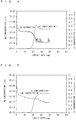
- FIGS, 2 to 5 are diagrams showing the relationship between a distribution of elements and the presence or absence of the anti-diffusion layer 6.
- FIGS. 2 and 3 show depth profiles of Ga element, Al element, and In element measured by means of auger electron spectroscopy with respect to two types of epitaxial substrates 10 that were prepared under the same conditions except for the presence or absence of the anti-diffusion layer 6.
- FIG. 2 shows a depth profile for the epitaxial substrate 10 including the anti-diffusion layer 6.
- FIG. 3 shows a depth profile for the epitaxial substrate 10 not including the anti-diffusion layer 6.
- the barrier layer 5 is made of In 0.18 Al 0.82 N and the cap layer 7 is made of GaN.
- the position indicated by the Sputter time being 0 min. corresponds to a surface of the epitaxial substrate 10 (a surface of the cap layer 7), and a greater value of the Sputter time indicates a position farther from the surface,
- FIGS. 4 and 5 show concentration profiles of Mg element and Al element measured by means of SIMS (secondary ion mass spectrometry) with respect to two types of epitaxial substrates 10 that were prepared under the same conditions except for the presence or absence of the anti-diffusion layer 6.
- FIG. 4 shows a concentration profile for the epitaxial substrate 10 including the anti-diffusion layer 6.
- FIG. 5 shows a concentration profile for the epitaxial substrate 10 not including the anti-diffusion layer 6.
- the barrier layer 5 is made of In 0.18 Al 0.82 N and the cap layer 7 is made of GaN doped with Mg.
- the Mg concentration steeply drops, while around when the surface depth is 20 nm to 25 nm, the Al concentration steeply rises and forms a peak around when the surface depth is 24 nm. It is considered that this peak corresponds to the AlN layer serving as the anti-diffusion layer 6. In a range where the surface depth is greater than 28 nm, the Al concentration is substantially constant.
- the Mg concentration gently drops.
- the Al concentration rises. In the profile of the Al concentration, no peak is observed.
- the epitaxial substrate 10 including the cap layer 7 and the anti-diffusion layer 6 excellent characteristics are achieved, as compared with an epitaxial substrate including only the cap layer 7 and not including the anti-diffusion layer 6.
- the cap layer 7 even when the cap layer 7 is provided, a sheet resistance, a concentration of the two-dimensional electron gas, and a mobility of the two-dimensional electron gas, that are equivalent to those of an epitaxial substrate not including the cap layer 7, are achieved.
- the cap layer 7 is made of GaN doped with Mg as an acceptor element to thereby form a PN junction, a reverse leakage current occurring in the PN junction is reduced to 1 nA or less.
- the thickness of the anti-diffusion layer 6 is 3 nm or more. Even when the thickness is less than 3 nm, a diffusion prevention effect is obtained to a certain degree, but from the viewpoint of reliably ensuring good electrical characteristics, it is preferable that the anti-diffusion layer 6 is formed with a thickness of 3 nm or more.
- the cap layer is provided on the barrier layer, and additionally an AlN layer serving as an anti-diffusion layer is provided between the layers.
- an epitaxial substrate diffusion of elements from the cap layer to the barrier layer is prevented.
- an epitaxial substrate including a cap layer and having excellent characteristics is achieved.
- a semiconductor element or a PN junction diode element including the epitaxial substrate is achieved.
- the composition of the barrier layer 5 three different levels were provided.
- the film thickness of the anti-diffusion layer 6 five different levels were provided, including a case where the anti-diffusion layer 6 was not provided (film thickness was 0 nm).
- the composition of the cap layer 7 four different levels were provided, including a case where the cap layer 7 is not provided.
- the film thickness of the cap layer 7 two different levels were provided, including a case where the cap layer 7 is not provided.
- Each of the obtained epitaxial substrates 10 was evaluated for electrical characteristics by using the Hall effect method.
- a plurality of (0001)-oriented 6H-SiC substrates having a diameter of two inches were prepared as the base substrate 1.
- the thickness thereof was 300 ⁇ m.
- Each of the substrates was placed in a reactor of an MOCVD apparatus, and the inside of the reactor was vacuumed. Then, the pressure in the reactor was set to be 30 kPa, and an atmosphere in a hydrogen/nitrogen mixed flow state was made. Then, the susceptor was heated, to thereby raise the temperature of the base substrate 1.
- a TMA bubbling gas and an ammonia gas were introduced into the reactor, and an AlN layer having a thickness of 200 nm was formed as the buffer layer.
- the temperature of the susceptor was set to be a predetermined temperature
- a TMG bubbling gas serving as the metal organic source gas and an ammonia gas were introduced into the reactor with a predetermined flow ratio.
- a GaN layer serving as the channel layer 3 was formed with a thickness of 2 ⁇ m.
- the pressure in the reactor was set to be 10 kPa, and then a TMA bubbling gas and an ammonia gas were introduced into the reactor.
- a TMA bubbling gas and an ammonia gas were introduced into the reactor.
- an AlN layer having a thickness of 1 nm was formed as the spacer layer 4.
- the barrier layer 5 was then formed.
- an AlN layer serving as the anti-diffusion layer 6 was formed with a thickness of 1.5, 3, 6 or 10 nm.
- the temperature of the susceptor was 800°C.
- the cap layer 7 was formed with a thickness of 10 nm or 50 nm.
- the temperature of the susceptor was 800°C.
- the temperature of the susceptor was dropped to about the room temperature. After the inside of the reactor was returned to the atmospheric pressure, the prepared epitaxial substrate 10 was taken out. Through the above-described procedures, each of the epitaxial substrates 10 was obtained.
- a multilayer metal film made of Ti/Al/Ni/Au (with film thicknesses of 25, 75, 15, and 100 nm, respectively) was vapor-deposited on the surface of each epitaxial substrate 10 (the surface of the cap layer 7), to form an ohmic electrode. Then, to give good contact characteristics to this electrode, a heat treatment was performed for 30 seconds in a nitrogen gas atmosphere at 800°C.
- the epitaxial substrate 10 in which the electrode was formed in this manner was measured for a two-dimensional electron gas concentration (2DEG concentration), a two-dimensional electron gas mobility (2DEG mobility), and a sheet resistance by means of the Hall effect method.
- Preparation conditions unique to each of the epitaxial substrates 10, and results of evaluation of electrical characteristics are listed in Tables 1 to 3. [Table 1] Sample No.
- Tables 1 to 3 reveal that, irrespective of the composition of the barrier layer 5, electrical characteristics obtained in the epitaxial substrates 10 (sample Nos. 1-4 to 1-6, 1-10 to 1-12, 1-16 to 1-18, 1-22 to 1-24, 1-28 to 1-30, 1-34 to 1-36, 1-40 to 1-42, 1-46 to 1-48, and 1-52 to 1-54) in which the cap layer 7 was formed after the formation of the anti-diffusion layer 6 with a thickness of 3 nm or more were equivalent to electrical characteristics of the epitaxial substrates 10 (sample Nos. 1-2, 1-8, 1-14, 1-20, 1-26, 1-32, 1-38, 1-44, and 1-50) in which the anti-diffusion layer 6 and the cap layer 7 were not provided.
- the epitaxial substrate 10 (sample Nos. 1-23) including the anti-diffusion layer 6 and the epitaxial substrate 10 (sample Nos. 1-20) not including the anti-diffusion layer 6, a depth profile of the Ga element, the Al element, and the In element was obtained by means of the auger electron spectroscopy.
- FIG. 2 shows a result for the former
- FIG. 3 shows a result for the latter.
- the diffusion of the Ga element from the cap layer 7 to the barrier layer 5 is observed, while from FIG. 2 , it is observed that the diffusion of the Ga element from the cap layer 7 to the barrier layer 5 is suitably prevented by the anti-diffusion layer 6.
- the electrical characteristics were improved as compared with the epitaxial substrate 10 not including the anti-diffusion layer 6. That is, the diffusion prevention effect of the anti-diffusion layer 6 is, though limited, obtained.
- the composition of the barrier layer 5 three different levels were provided.
- the film thickness of the anti-diffusion layer 6 five different levels were provided, including a case where the anti-diffusion layer 6 was not provided (film thickness was 0 nm).
- a target concentration of the Mg element doped as an acceptor element in the cap layer 7 three different levels were provided.
- Each of the epitaxial substrates 10 was used to prepare a concentric PN diode element, and its leakage current (reverse leakage current) at a time when reverse bias was applied was measured.
- the cap layer 7 was formed in a manner that Mg serving as an acceptor element was doped into the GaN layer, after the formation of the barrier layer 5 or the anti-diffusion layer 6.
- Mg serving as an acceptor element was doped into the GaN layer, after the formation of the barrier layer 5 or the anti-diffusion layer 6.
- the target concentration of the Mg element three different levels, namely, 1.0 ⁇ 10 18 /cm 3 , 1.0 ⁇ 10 19 /cm 3 , and 5.0 ⁇ 10 19 /cm 3 , were adopted.
- the thickness was 50 nm.
- the temperature of the susceptor was 950°C.
- the cap layer 7 was formed, and then the temperature of the susceptor was dropped to about the room temperature. After the inside of the reactor was returned to the atmospheric pressure, the prepared epitaxial substrate 10 was taken out. Then, the sample in which the cap layer 7 was formed was subjected to a heat treatment for 30 minutes in a nitrogen gas atmosphere at 600°C, for activating the Mg acceptor. Through the above-described procedures, the respective epitaxial substrates 10 were obtained.
- a concentric PN diode element including a central circular electrode as a P-type electrode and an outer ring electrode as an n-type electrode.
- RIE reactive ion etching
- a multilayer metal electrode made of Ti/Al/Ni/Au (with film thicknesses of 25, 75, 15, and 100 nm, respectively) was vapor-deposited on the surface of the exposed portion of the barrier layer 5, to form an ohmic n-type electrode. Then, to give good contact characteristics to this n-type electrode, a heat treatment was performed for 30 seconds in a nitrogen gas atmosphere at 800°C.
- a multilayer metal electrode made of Ni/Au (with film thicknesses of 20 nm and 200 nm) was vapor-deposited on a remaining surface portion (central portion of the concentric circle) of the epitaxial substrate 10 that was not removed in the RIE process.
- an ohmic p-type electrode was formed.
- the p-type electrode was formed with a circular shape having a diameter of 1 mm in a plan view. Furthermore, to give good contact characteristics to this p-type electrode, a heat treatment was performed for 30 seconds in a nitrogen gas atmosphere at 500°C. Thereby, a concentric PN diode element was obtained.
- Tables 4 to 6 reveal that, a reverse leakage current in the order of ⁇ A occurred in the epitaxial substrates 10 (sample Nos. 2-1, 2-6, 2-11, 2-16, 2-21, 2-26, 2-31, 2-36, and 2-41) in which the cap layer 7 was formed without forming the anti-diffusion layer 6 and in the epitaxial substrates 10 (sample Nos.
- cap layer 7 was formed after the anti-diffusion layer 6 with a thickness of 1.5 nm was formed, while the reverse leakage current was reduced to 1 nA or less in the epitaxial substrates 10 (sample Nos, 2-3 to 2-5, 2-8 to 2-10, 2-13 to 2-15, 2-18 to 2-20, 2-23 to 2-25, 2-28 to 2-30, 2-33 to 2-35, 2-38 to 2-40, and 2-42 to 2-45) in which the cap layer 7 was formed after the anti-diffusion layer 6 with a thickness of 3 nm or more was formed.
- FIG. 4 shows a result for the former
- FIG. 5 shows a result for the latter.
- the diffusion of the Mg element from the cap layer 7 to the barrier layer 5 is observed, while from FIG. 4 , it is observed that the diffusion of the Mg element from the cap layer 7 to the barrier layer 5 is suitably prevented by the anti-diffusion layer 6.
Landscapes
- Engineering & Computer Science (AREA)
- Power Engineering (AREA)
- Microelectronics & Electronic Packaging (AREA)
- Chemical & Material Sciences (AREA)
- Physics & Mathematics (AREA)
- Computer Hardware Design (AREA)
- General Physics & Mathematics (AREA)
- Condensed Matter Physics & Semiconductors (AREA)
- Ceramic Engineering (AREA)
- Crystallography & Structural Chemistry (AREA)
- Organic Chemistry (AREA)
- Metallurgy (AREA)
- Materials Engineering (AREA)
- Manufacturing & Machinery (AREA)
- General Chemical & Material Sciences (AREA)
- Chemical Kinetics & Catalysis (AREA)
- Inorganic Chemistry (AREA)
- Junction Field-Effect Transistors (AREA)
- Recrystallisation Techniques (AREA)
Applications Claiming Priority (2)
| Application Number | Priority Date | Filing Date | Title |
|---|---|---|---|
| JP2010170320 | 2010-07-29 | ||
| PCT/JP2011/066948 WO2012014883A1 (ja) | 2010-07-29 | 2011-07-26 | 半導体素子用エピタキシャル基板、半導体素子、pn接合ダイオード素子、および半導体素子用エピタキシャル基板の製造方法 |
Publications (3)
| Publication Number | Publication Date |
|---|---|
| EP2600394A1 EP2600394A1 (en) | 2013-06-05 |
| EP2600394A4 EP2600394A4 (en) | 2014-10-01 |
| EP2600394B1 true EP2600394B1 (en) | 2017-12-27 |
Family
ID=45530090
Family Applications (1)
| Application Number | Title | Priority Date | Filing Date |
|---|---|---|---|
| EP11812472.6A Not-in-force EP2600394B1 (en) | 2010-07-29 | 2011-07-26 | Epitaxial substrate for semiconductor element and production method thereof |
Country Status (5)
| Country | Link |
|---|---|
| US (1) | US9024325B2 (zh) |
| EP (1) | EP2600394B1 (zh) |
| JP (1) | JP5782033B2 (zh) |
| CN (1) | CN103003931B (zh) |
| WO (1) | WO2012014883A1 (zh) |
Families Citing this family (15)
| Publication number | Priority date | Publication date | Assignee | Title |
|---|---|---|---|---|
| WO2013185089A1 (en) * | 2012-06-07 | 2013-12-12 | Iqe Kc, Llc | Double aluminum nitride spacers for nitride high electron-mobility transistors |
| WO2014024310A1 (ja) * | 2012-08-10 | 2014-02-13 | 日本碍子株式会社 | 半導体素子、hemt素子、および半導体素子の製造方法 |
| JP6318474B2 (ja) * | 2013-06-07 | 2018-05-09 | 住友電気工業株式会社 | 半導体装置の製造方法 |
| JP6179266B2 (ja) * | 2013-08-12 | 2017-08-16 | 富士通株式会社 | 半導体装置及び半導体装置の製造方法 |
| WO2015068448A1 (ja) * | 2013-11-06 | 2015-05-14 | シャープ株式会社 | 窒化物半導体 |
| JP2015165530A (ja) * | 2014-03-03 | 2015-09-17 | 三菱電機株式会社 | 半導体装置および半導体装置の製造方法 |
| WO2016181441A1 (ja) * | 2015-05-08 | 2016-11-17 | 富士通株式会社 | 半導体装置及び半導体装置の製造方法 |
| JP6792135B2 (ja) * | 2015-10-30 | 2020-11-25 | 富士通株式会社 | 化合物半導体装置及びその製造方法 |
| KR102547562B1 (ko) * | 2015-11-02 | 2023-06-23 | 엔지케이 인슐레이터 엘티디 | 반도체 소자용 에피택셜 기판, 반도체 소자, 및 반도체 소자용 에피택셜 기판의 제조 방법 |
| JP6870304B2 (ja) * | 2016-12-05 | 2021-05-12 | 住友電気工業株式会社 | 半導体装置の製造方法 |
| WO2019106843A1 (ja) * | 2017-12-01 | 2019-06-06 | 三菱電機株式会社 | 半導体装置の製造方法、半導体装置 |
| TWI701836B (zh) * | 2019-07-26 | 2020-08-11 | 新唐科技股份有限公司 | 增強型高電子遷移率電晶體元件及其製造方法 |
| CN111477536A (zh) | 2020-03-31 | 2020-07-31 | 华为技术有限公司 | 一种半导体外延结构及半导体器件 |
| CN111354629B (zh) * | 2020-04-26 | 2023-04-07 | 江西力特康光学有限公司 | 一种用于紫外LED的AlN缓冲层结构及其制作方法 |
| US20240105823A1 (en) * | 2022-09-23 | 2024-03-28 | Wolfspeed, Inc. | Barrier Structure for Dispersion Reduction in Transistor Devices |
Family Cites Families (17)
| Publication number | Priority date | Publication date | Assignee | Title |
|---|---|---|---|---|
| JP3761589B2 (ja) * | 1993-03-26 | 2006-03-29 | 豊田合成株式会社 | 窒化ガリウム系化合物半導体発光素子 |
| CN100375301C (zh) * | 2002-11-06 | 2008-03-12 | 三垦电气株式会社 | 半导体发光元件及其制造方法 |
| SG135924A1 (en) * | 2003-04-02 | 2007-10-29 | Sumitomo Electric Industries | Nitride-based semiconductor epitaxial substrate, method of manufacturing the same, and hemt substrate |
| US7282744B2 (en) * | 2003-05-09 | 2007-10-16 | Cree, Inc. | III-nitride optoelectronic device structure with high Al AlGaN diffusion barrier |
| JP2005268493A (ja) * | 2004-03-18 | 2005-09-29 | National Institute Of Information & Communication Technology | ヘテロ接合電界効果トランジスタ |
| US7709859B2 (en) * | 2004-11-23 | 2010-05-04 | Cree, Inc. | Cap layers including aluminum nitride for nitride-based transistors |
| US7456443B2 (en) * | 2004-11-23 | 2008-11-25 | Cree, Inc. | Transistors having buried n-type and p-type regions beneath the source region |
| US7928462B2 (en) * | 2006-02-16 | 2011-04-19 | Lg Electronics Inc. | Light emitting device having vertical structure, package thereof and method for manufacturing the same |
| JP4932305B2 (ja) * | 2006-03-30 | 2012-05-16 | 株式会社豊田中央研究所 | Iii族窒化物系化合物半導体素子の製造方法 |
| JP5201437B2 (ja) * | 2006-11-30 | 2013-06-05 | 国立大学法人 名古屋工業大学 | 絶縁ゲート電界効果トランジスタ |
| JP2008235613A (ja) * | 2007-03-22 | 2008-10-02 | Eudyna Devices Inc | 半導体装置 |
| JP4920519B2 (ja) * | 2007-07-26 | 2012-04-18 | 株式会社豊田中央研究所 | 窒化物半導体装置とその製造方法 |
| JP2009054623A (ja) * | 2007-08-23 | 2009-03-12 | Toshiba Corp | 半導体装置 |
| US7915643B2 (en) * | 2007-09-17 | 2011-03-29 | Transphorm Inc. | Enhancement mode gallium nitride power devices |
| JP2009231396A (ja) * | 2008-03-19 | 2009-10-08 | Sumitomo Chemical Co Ltd | 半導体装置および半導体装置の製造方法 |
| EP2259287A4 (en) * | 2008-03-24 | 2012-08-15 | Ngk Insulators Ltd | EPITACTICAL SUBSTRATE FOR A SEMICONDUCTOR COMPONENT, SEMICONDUCTOR COMPONENT AND METHOD FOR PRODUCING AN EPITACTICAL SUBSTRATE FOR A SEMICONDUCTOR COMPONENT |
| JP5509544B2 (ja) * | 2008-06-11 | 2014-06-04 | 富士通株式会社 | 半導体装置及びその製造方法 |
-
2011
- 2011-07-26 EP EP11812472.6A patent/EP2600394B1/en not_active Not-in-force
- 2011-07-26 CN CN201180035034.9A patent/CN103003931B/zh not_active Expired - Fee Related
- 2011-07-26 WO PCT/JP2011/066948 patent/WO2012014883A1/ja active Application Filing
- 2011-07-26 JP JP2012526510A patent/JP5782033B2/ja not_active Expired - Fee Related
-
2013
- 2013-01-22 US US13/746,879 patent/US9024325B2/en active Active
Non-Patent Citations (1)
| Title |
|---|
| None * |
Also Published As
| Publication number | Publication date |
|---|---|
| CN103003931B (zh) | 2016-01-13 |
| CN103003931A (zh) | 2013-03-27 |
| JP5782033B2 (ja) | 2015-09-24 |
| WO2012014883A1 (ja) | 2012-02-02 |
| JPWO2012014883A1 (ja) | 2013-09-12 |
| EP2600394A4 (en) | 2014-10-01 |
| EP2600394A1 (en) | 2013-06-05 |
| US9024325B2 (en) | 2015-05-05 |
| US20130134439A1 (en) | 2013-05-30 |
Similar Documents
| Publication | Publication Date | Title |
|---|---|---|
| EP2600394B1 (en) | Epitaxial substrate for semiconductor element and production method thereof | |
| JP5926216B2 (ja) | 埋込み層に低抵抗コンタクトを形成する打込み領域を含んだ半導体デバイスの製作方法および関連したデバイス | |
| US9478650B2 (en) | Semiconductor device, HEMT device, and method of manufacturing semiconductor device | |
| US8410552B2 (en) | Epitaxial substrate for semiconductor device, semiconductor device, and method of manufacturing epitaxial substrate for semiconductor device | |
| US8853735B2 (en) | Epitaxial substrate for semiconductor device and semiconductor device | |
| EP2290696B1 (en) | Epitaxial substrate for semiconductor device, semiconductor device, and method of manufacturing epitaxial substrate for semiconductor device | |
| JP2014022752A (ja) | 窒化物系半導体素子及びその製造方法 | |
| US9382641B2 (en) | Epitaxial substrate for semiconductor device, semiconductor device, and method of manufacturing epitaxial substrate for semiconductor device | |
| US7750351B2 (en) | Epitaxial substrate for field effect transistor | |
| US20120168771A1 (en) | Semiconductor element, hemt element, and method of manufacturing semiconductor element | |
| US8598626B2 (en) | Epitaxial substrate for semiconductor device, schottky junction structure, and leakage current suppression method for schottky junction structure | |
| JP5806545B2 (ja) | 半導体素子、hemt素子、および半導体素子の製造方法 | |
| JP5583610B2 (ja) | 半導体素子用エピタキシャル基板および半導体素子 | |
| JP2011222969A (ja) | 半導体素子用エピタキシャル基板の製造方法、半導体素子用エピタキシャル基板、および半導体素子 | |
| Nomoto et al. | Ion-Implanted GaN/AlGaN/GaN HEMTs with Extremely Low Gate Leakage Current |
Legal Events
| Date | Code | Title | Description |
|---|---|---|---|
| PUAI | Public reference made under article 153(3) epc to a published international application that has entered the european phase |
Free format text: ORIGINAL CODE: 0009012 |
|
| 17P | Request for examination filed |
Effective date: 20130128 |
|
| AK | Designated contracting states |
Kind code of ref document: A1 Designated state(s): AL AT BE BG CH CY CZ DE DK EE ES FI FR GB GR HR HU IE IS IT LI LT LU LV MC MK MT NL NO PL PT RO RS SE SI SK SM TR |
|
| DAX | Request for extension of the european patent (deleted) | ||
| A4 | Supplementary search report drawn up and despatched |
Effective date: 20140828 |
|
| RIC1 | Information provided on ipc code assigned before grant |
Ipc: H01L 29/861 20060101ALI20140822BHEP Ipc: H01L 21/338 20060101AFI20140822BHEP Ipc: H01L 21/205 20060101ALI20140822BHEP Ipc: C23C 16/34 20060101ALI20140822BHEP Ipc: H01L 29/778 20060101ALI20140822BHEP Ipc: H01L 29/812 20060101ALI20140822BHEP |
|
| GRAP | Despatch of communication of intention to grant a patent |
Free format text: ORIGINAL CODE: EPIDOSNIGR1 |
|
| INTG | Intention to grant announced |
Effective date: 20170608 |
|
| GRAS | Grant fee paid |
Free format text: ORIGINAL CODE: EPIDOSNIGR3 |
|
| GRAJ | Information related to disapproval of communication of intention to grant by the applicant or resumption of examination proceedings by the epo deleted |
Free format text: ORIGINAL CODE: EPIDOSDIGR1 |
|
| GRAL | Information related to payment of fee for publishing/printing deleted |
Free format text: ORIGINAL CODE: EPIDOSDIGR3 |
|
| GRAR | Information related to intention to grant a patent recorded |
Free format text: ORIGINAL CODE: EPIDOSNIGR71 |
|
| INTC | Intention to grant announced (deleted) | ||
| INTG | Intention to grant announced |
Effective date: 20171016 |
|
| GRAA | (expected) grant |
Free format text: ORIGINAL CODE: 0009210 |
|
| AK | Designated contracting states |
Kind code of ref document: B1 Designated state(s): AL AT BE BG CH CY CZ DE DK EE ES FI FR GB GR HR HU IE IS IT LI LT LU LV MC MK MT NL NO PL PT RO RS SE SI SK SM TR |
|
| REG | Reference to a national code |
Ref country code: GB Ref legal event code: FG4D |
|
| REG | Reference to a national code |
Ref country code: CH Ref legal event code: EP |
|
| REG | Reference to a national code |
Ref country code: AT Ref legal event code: REF Ref document number: 958986 Country of ref document: AT Kind code of ref document: T Effective date: 20180115 |
|
| REG | Reference to a national code |
Ref country code: IE Ref legal event code: FG4D |
|
| REG | Reference to a national code |
Ref country code: DE Ref legal event code: R096 Ref document number: 602011044596 Country of ref document: DE |
|
| PG25 | Lapsed in a contracting state [announced via postgrant information from national office to epo] |
Ref country code: LT Free format text: LAPSE BECAUSE OF FAILURE TO SUBMIT A TRANSLATION OF THE DESCRIPTION OR TO PAY THE FEE WITHIN THE PRESCRIBED TIME-LIMIT Effective date: 20171227 Ref country code: FI Free format text: LAPSE BECAUSE OF FAILURE TO SUBMIT A TRANSLATION OF THE DESCRIPTION OR TO PAY THE FEE WITHIN THE PRESCRIBED TIME-LIMIT Effective date: 20171227 Ref country code: NO Free format text: LAPSE BECAUSE OF FAILURE TO SUBMIT A TRANSLATION OF THE DESCRIPTION OR TO PAY THE FEE WITHIN THE PRESCRIBED TIME-LIMIT Effective date: 20180327 |
|
| REG | Reference to a national code |
Ref country code: NL Ref legal event code: MP Effective date: 20171227 |
|
| REG | Reference to a national code |
Ref country code: LT Ref legal event code: MG4D |
|
| REG | Reference to a national code |
Ref country code: AT Ref legal event code: MK05 Ref document number: 958986 Country of ref document: AT Kind code of ref document: T Effective date: 20171227 |
|
| PG25 | Lapsed in a contracting state [announced via postgrant information from national office to epo] |
Ref country code: BG Free format text: LAPSE BECAUSE OF FAILURE TO SUBMIT A TRANSLATION OF THE DESCRIPTION OR TO PAY THE FEE WITHIN THE PRESCRIBED TIME-LIMIT Effective date: 20180327 Ref country code: RS Free format text: LAPSE BECAUSE OF FAILURE TO SUBMIT A TRANSLATION OF THE DESCRIPTION OR TO PAY THE FEE WITHIN THE PRESCRIBED TIME-LIMIT Effective date: 20171227 Ref country code: HR Free format text: LAPSE BECAUSE OF FAILURE TO SUBMIT A TRANSLATION OF THE DESCRIPTION OR TO PAY THE FEE WITHIN THE PRESCRIBED TIME-LIMIT Effective date: 20171227 Ref country code: GR Free format text: LAPSE BECAUSE OF FAILURE TO SUBMIT A TRANSLATION OF THE DESCRIPTION OR TO PAY THE FEE WITHIN THE PRESCRIBED TIME-LIMIT Effective date: 20180328 Ref country code: LV Free format text: LAPSE BECAUSE OF FAILURE TO SUBMIT A TRANSLATION OF THE DESCRIPTION OR TO PAY THE FEE WITHIN THE PRESCRIBED TIME-LIMIT Effective date: 20171227 |
|
| PG25 | Lapsed in a contracting state [announced via postgrant information from national office to epo] |
Ref country code: NL Free format text: LAPSE BECAUSE OF FAILURE TO SUBMIT A TRANSLATION OF THE DESCRIPTION OR TO PAY THE FEE WITHIN THE PRESCRIBED TIME-LIMIT Effective date: 20171227 |
|
| PG25 | Lapsed in a contracting state [announced via postgrant information from national office to epo] |
Ref country code: ES Free format text: LAPSE BECAUSE OF FAILURE TO SUBMIT A TRANSLATION OF THE DESCRIPTION OR TO PAY THE FEE WITHIN THE PRESCRIBED TIME-LIMIT Effective date: 20171227 Ref country code: CZ Free format text: LAPSE BECAUSE OF FAILURE TO SUBMIT A TRANSLATION OF THE DESCRIPTION OR TO PAY THE FEE WITHIN THE PRESCRIBED TIME-LIMIT Effective date: 20171227 Ref country code: SK Free format text: LAPSE BECAUSE OF FAILURE TO SUBMIT A TRANSLATION OF THE DESCRIPTION OR TO PAY THE FEE WITHIN THE PRESCRIBED TIME-LIMIT Effective date: 20171227 Ref country code: CY Free format text: LAPSE BECAUSE OF FAILURE TO SUBMIT A TRANSLATION OF THE DESCRIPTION OR TO PAY THE FEE WITHIN THE PRESCRIBED TIME-LIMIT Effective date: 20171227 Ref country code: EE Free format text: LAPSE BECAUSE OF FAILURE TO SUBMIT A TRANSLATION OF THE DESCRIPTION OR TO PAY THE FEE WITHIN THE PRESCRIBED TIME-LIMIT Effective date: 20171227 |
|
| PG25 | Lapsed in a contracting state [announced via postgrant information from national office to epo] |
Ref country code: PL Free format text: LAPSE BECAUSE OF FAILURE TO SUBMIT A TRANSLATION OF THE DESCRIPTION OR TO PAY THE FEE WITHIN THE PRESCRIBED TIME-LIMIT Effective date: 20171227 Ref country code: SM Free format text: LAPSE BECAUSE OF FAILURE TO SUBMIT A TRANSLATION OF THE DESCRIPTION OR TO PAY THE FEE WITHIN THE PRESCRIBED TIME-LIMIT Effective date: 20171227 Ref country code: IS Free format text: LAPSE BECAUSE OF FAILURE TO SUBMIT A TRANSLATION OF THE DESCRIPTION OR TO PAY THE FEE WITHIN THE PRESCRIBED TIME-LIMIT Effective date: 20180427 Ref country code: RO Free format text: LAPSE BECAUSE OF FAILURE TO SUBMIT A TRANSLATION OF THE DESCRIPTION OR TO PAY THE FEE WITHIN THE PRESCRIBED TIME-LIMIT Effective date: 20171227 Ref country code: AT Free format text: LAPSE BECAUSE OF FAILURE TO SUBMIT A TRANSLATION OF THE DESCRIPTION OR TO PAY THE FEE WITHIN THE PRESCRIBED TIME-LIMIT Effective date: 20171227 Ref country code: IT Free format text: LAPSE BECAUSE OF FAILURE TO SUBMIT A TRANSLATION OF THE DESCRIPTION OR TO PAY THE FEE WITHIN THE PRESCRIBED TIME-LIMIT Effective date: 20171227 |
|
| REG | Reference to a national code |
Ref country code: DE Ref legal event code: R097 Ref document number: 602011044596 Country of ref document: DE |
|
| PLBE | No opposition filed within time limit |
Free format text: ORIGINAL CODE: 0009261 |
|
| STAA | Information on the status of an ep patent application or granted ep patent |
Free format text: STATUS: NO OPPOSITION FILED WITHIN TIME LIMIT |
|
| PG25 | Lapsed in a contracting state [announced via postgrant information from national office to epo] |
Ref country code: DK Free format text: LAPSE BECAUSE OF FAILURE TO SUBMIT A TRANSLATION OF THE DESCRIPTION OR TO PAY THE FEE WITHIN THE PRESCRIBED TIME-LIMIT Effective date: 20171227 |
|
| 26N | No opposition filed |
Effective date: 20180928 |
|
| PG25 | Lapsed in a contracting state [announced via postgrant information from national office to epo] |
Ref country code: SI Free format text: LAPSE BECAUSE OF FAILURE TO SUBMIT A TRANSLATION OF THE DESCRIPTION OR TO PAY THE FEE WITHIN THE PRESCRIBED TIME-LIMIT Effective date: 20171227 |
|
| REG | Reference to a national code |
Ref country code: CH Ref legal event code: PL |
|
| GBPC | Gb: european patent ceased through non-payment of renewal fee |
Effective date: 20180726 |
|
| PG25 | Lapsed in a contracting state [announced via postgrant information from national office to epo] |
Ref country code: LU Free format text: LAPSE BECAUSE OF NON-PAYMENT OF DUE FEES Effective date: 20180726 Ref country code: MC Free format text: LAPSE BECAUSE OF FAILURE TO SUBMIT A TRANSLATION OF THE DESCRIPTION OR TO PAY THE FEE WITHIN THE PRESCRIBED TIME-LIMIT Effective date: 20171227 |
|
| REG | Reference to a national code |
Ref country code: BE Ref legal event code: MM Effective date: 20180731 |
|
| REG | Reference to a national code |
Ref country code: IE Ref legal event code: MM4A |
|
| PG25 | Lapsed in a contracting state [announced via postgrant information from national office to epo] |
Ref country code: IE Free format text: LAPSE BECAUSE OF NON-PAYMENT OF DUE FEES Effective date: 20180726 Ref country code: CH Free format text: LAPSE BECAUSE OF NON-PAYMENT OF DUE FEES Effective date: 20180731 Ref country code: GB Free format text: LAPSE BECAUSE OF NON-PAYMENT OF DUE FEES Effective date: 20180726 Ref country code: LI Free format text: LAPSE BECAUSE OF NON-PAYMENT OF DUE FEES Effective date: 20180731 Ref country code: FR Free format text: LAPSE BECAUSE OF NON-PAYMENT OF DUE FEES Effective date: 20180731 |
|
| PG25 | Lapsed in a contracting state [announced via postgrant information from national office to epo] |
Ref country code: BE Free format text: LAPSE BECAUSE OF NON-PAYMENT OF DUE FEES Effective date: 20180731 |
|
| PG25 | Lapsed in a contracting state [announced via postgrant information from national office to epo] |
Ref country code: MT Free format text: LAPSE BECAUSE OF NON-PAYMENT OF DUE FEES Effective date: 20180726 |
|
| PG25 | Lapsed in a contracting state [announced via postgrant information from national office to epo] |
Ref country code: TR Free format text: LAPSE BECAUSE OF FAILURE TO SUBMIT A TRANSLATION OF THE DESCRIPTION OR TO PAY THE FEE WITHIN THE PRESCRIBED TIME-LIMIT Effective date: 20171227 |
|
| PG25 | Lapsed in a contracting state [announced via postgrant information from national office to epo] |
Ref country code: PT Free format text: LAPSE BECAUSE OF FAILURE TO SUBMIT A TRANSLATION OF THE DESCRIPTION OR TO PAY THE FEE WITHIN THE PRESCRIBED TIME-LIMIT Effective date: 20171227 Ref country code: HU Free format text: LAPSE BECAUSE OF FAILURE TO SUBMIT A TRANSLATION OF THE DESCRIPTION OR TO PAY THE FEE WITHIN THE PRESCRIBED TIME-LIMIT; INVALID AB INITIO Effective date: 20110726 |
|
| PG25 | Lapsed in a contracting state [announced via postgrant information from national office to epo] |
Ref country code: MK Free format text: LAPSE BECAUSE OF NON-PAYMENT OF DUE FEES Effective date: 20171227 Ref country code: SE Free format text: LAPSE BECAUSE OF FAILURE TO SUBMIT A TRANSLATION OF THE DESCRIPTION OR TO PAY THE FEE WITHIN THE PRESCRIBED TIME-LIMIT Effective date: 20171227 |
|
| PG25 | Lapsed in a contracting state [announced via postgrant information from national office to epo] |
Ref country code: AL Free format text: LAPSE BECAUSE OF FAILURE TO SUBMIT A TRANSLATION OF THE DESCRIPTION OR TO PAY THE FEE WITHIN THE PRESCRIBED TIME-LIMIT Effective date: 20171227 |
|
| PGFP | Annual fee paid to national office [announced via postgrant information from national office to epo] |
Ref country code: DE Payment date: 20220531 Year of fee payment: 12 |
|
| REG | Reference to a national code |
Ref country code: DE Ref legal event code: R119 Ref document number: 602011044596 Country of ref document: DE |
|
| PG25 | Lapsed in a contracting state [announced via postgrant information from national office to epo] |
Ref country code: DE Free format text: LAPSE BECAUSE OF NON-PAYMENT OF DUE FEES Effective date: 20240201 |