EP2588636B1 - Molybdenum containing targets - Google Patents
Molybdenum containing targets Download PDFInfo
- Publication number
- EP2588636B1 EP2588636B1 EP10730332.3A EP10730332A EP2588636B1 EP 2588636 B1 EP2588636 B1 EP 2588636B1 EP 10730332 A EP10730332 A EP 10730332A EP 2588636 B1 EP2588636 B1 EP 2588636B1
- Authority
- EP
- European Patent Office
- Prior art keywords
- sputter target
- atomic
- molybdenum
- metal element
- phase
- Prior art date
- Legal status (The legal status is an assumption and is not a legal conclusion. Google has not performed a legal analysis and makes no representation as to the accuracy of the status listed.)
- Not-in-force
Links
Images


Classifications
-
- C—CHEMISTRY; METALLURGY
- C23—COATING METALLIC MATERIAL; COATING MATERIAL WITH METALLIC MATERIAL; CHEMICAL SURFACE TREATMENT; DIFFUSION TREATMENT OF METALLIC MATERIAL; COATING BY VACUUM EVAPORATION, BY SPUTTERING, BY ION IMPLANTATION OR BY CHEMICAL VAPOUR DEPOSITION, IN GENERAL; INHIBITING CORROSION OF METALLIC MATERIAL OR INCRUSTATION IN GENERAL
- C23C—COATING METALLIC MATERIAL; COATING MATERIAL WITH METALLIC MATERIAL; SURFACE TREATMENT OF METALLIC MATERIAL BY DIFFUSION INTO THE SURFACE, BY CHEMICAL CONVERSION OR SUBSTITUTION; COATING BY VACUUM EVAPORATION, BY SPUTTERING, BY ION IMPLANTATION OR BY CHEMICAL VAPOUR DEPOSITION, IN GENERAL
- C23C14/00—Coating by vacuum evaporation, by sputtering or by ion implantation of the coating forming material
- C23C14/06—Coating by vacuum evaporation, by sputtering or by ion implantation of the coating forming material characterised by the coating material
- C23C14/14—Metallic material, boron or silicon
- C23C14/18—Metallic material, boron or silicon on other inorganic substrates
- C23C14/185—Metallic material, boron or silicon on other inorganic substrates by cathodic sputtering
-
- C—CHEMISTRY; METALLURGY
- C22—METALLURGY; FERROUS OR NON-FERROUS ALLOYS; TREATMENT OF ALLOYS OR NON-FERROUS METALS
- C22C—ALLOYS
- C22C27/00—Alloys based on rhenium or a refractory metal not mentioned in groups C22C14/00 or C22C16/00
- C22C27/04—Alloys based on tungsten or molybdenum
-
- C—CHEMISTRY; METALLURGY
- C23—COATING METALLIC MATERIAL; COATING MATERIAL WITH METALLIC MATERIAL; CHEMICAL SURFACE TREATMENT; DIFFUSION TREATMENT OF METALLIC MATERIAL; COATING BY VACUUM EVAPORATION, BY SPUTTERING, BY ION IMPLANTATION OR BY CHEMICAL VAPOUR DEPOSITION, IN GENERAL; INHIBITING CORROSION OF METALLIC MATERIAL OR INCRUSTATION IN GENERAL
- C23C—COATING METALLIC MATERIAL; COATING MATERIAL WITH METALLIC MATERIAL; SURFACE TREATMENT OF METALLIC MATERIAL BY DIFFUSION INTO THE SURFACE, BY CHEMICAL CONVERSION OR SUBSTITUTION; COATING BY VACUUM EVAPORATION, BY SPUTTERING, BY ION IMPLANTATION OR BY CHEMICAL VAPOUR DEPOSITION, IN GENERAL
- C23C14/00—Coating by vacuum evaporation, by sputtering or by ion implantation of the coating forming material
- C23C14/22—Coating by vacuum evaporation, by sputtering or by ion implantation of the coating forming material characterised by the process of coating
- C23C14/34—Sputtering
- C23C14/3407—Cathode assembly for sputtering apparatus, e.g. Target
- C23C14/3414—Metallurgical or chemical aspects of target preparation, e.g. casting, powder metallurgy
-
- C—CHEMISTRY; METALLURGY
- C23—COATING METALLIC MATERIAL; COATING MATERIAL WITH METALLIC MATERIAL; CHEMICAL SURFACE TREATMENT; DIFFUSION TREATMENT OF METALLIC MATERIAL; COATING BY VACUUM EVAPORATION, BY SPUTTERING, BY ION IMPLANTATION OR BY CHEMICAL VAPOUR DEPOSITION, IN GENERAL; INHIBITING CORROSION OF METALLIC MATERIAL OR INCRUSTATION IN GENERAL
- C23C—COATING METALLIC MATERIAL; COATING MATERIAL WITH METALLIC MATERIAL; SURFACE TREATMENT OF METALLIC MATERIAL BY DIFFUSION INTO THE SURFACE, BY CHEMICAL CONVERSION OR SUBSTITUTION; COATING BY VACUUM EVAPORATION, BY SPUTTERING, BY ION IMPLANTATION OR BY CHEMICAL VAPOUR DEPOSITION, IN GENERAL
- C23C14/00—Coating by vacuum evaporation, by sputtering or by ion implantation of the coating forming material
- C23C14/58—After-treatment
- C23C14/5873—Removal of material
-
- G—PHYSICS
- G06—COMPUTING OR CALCULATING; COUNTING
- G06F—ELECTRIC DIGITAL DATA PROCESSING
- G06F3/00—Input arrangements for transferring data to be processed into a form capable of being handled by the computer; Output arrangements for transferring data from processing unit to output unit, e.g. interface arrangements
- G06F3/01—Input arrangements or combined input and output arrangements for interaction between user and computer
- G06F3/03—Arrangements for converting the position or the displacement of a member into a coded form
- G06F3/041—Digitisers, e.g. for touch screens or touch pads, characterised by the transducing means
-
- B—PERFORMING OPERATIONS; TRANSPORTING
- B22—CASTING; POWDER METALLURGY
- B22F—WORKING METALLIC POWDER; MANUFACTURE OF ARTICLES FROM METALLIC POWDER; MAKING METALLIC POWDER; APPARATUS OR DEVICES SPECIALLY ADAPTED FOR METALLIC POWDER
- B22F2998/00—Supplementary information concerning processes or compositions relating to powder metallurgy
- B22F2998/10—Processes characterised by the sequence of their steps
-
- G—PHYSICS
- G06—COMPUTING OR CALCULATING; COUNTING
- G06F—ELECTRIC DIGITAL DATA PROCESSING
- G06F2203/00—Indexing scheme relating to G06F3/00 - G06F3/048
- G06F2203/041—Indexing scheme relating to G06F3/041 - G06F3/045
- G06F2203/04103—Manufacturing, i.e. details related to manufacturing processes specially suited for touch sensitive devices
-
- Y—GENERAL TAGGING OF NEW TECHNOLOGICAL DEVELOPMENTS; GENERAL TAGGING OF CROSS-SECTIONAL TECHNOLOGIES SPANNING OVER SEVERAL SECTIONS OF THE IPC; TECHNICAL SUBJECTS COVERED BY FORMER USPC CROSS-REFERENCE ART COLLECTIONS [XRACs] AND DIGESTS
- Y10—TECHNICAL SUBJECTS COVERED BY FORMER USPC
- Y10T—TECHNICAL SUBJECTS COVERED BY FORMER US CLASSIFICATION
- Y10T428/00—Stock material or miscellaneous articles
- Y10T428/12—All metal or with adjacent metals
- Y10T428/12493—Composite; i.e., plural, adjacent, spatially distinct metal components [e.g., layers, joint, etc.]
- Y10T428/12736—Al-base component
- Y10T428/12743—Next to refractory [Group IVB, VB, or VIB] metal-base component
-
- Y—GENERAL TAGGING OF NEW TECHNOLOGICAL DEVELOPMENTS; GENERAL TAGGING OF CROSS-SECTIONAL TECHNOLOGIES SPANNING OVER SEVERAL SECTIONS OF THE IPC; TECHNICAL SUBJECTS COVERED BY FORMER USPC CROSS-REFERENCE ART COLLECTIONS [XRACs] AND DIGESTS
- Y10—TECHNICAL SUBJECTS COVERED BY FORMER USPC
- Y10T—TECHNICAL SUBJECTS COVERED BY FORMER US CLASSIFICATION
- Y10T428/00—Stock material or miscellaneous articles
- Y10T428/12—All metal or with adjacent metals
- Y10T428/12493—Composite; i.e., plural, adjacent, spatially distinct metal components [e.g., layers, joint, etc.]
- Y10T428/12771—Transition metal-base component
- Y10T428/12806—Refractory [Group IVB, VB, or VIB] metal-base component
- Y10T428/12826—Group VIB metal-base component
-
- Y—GENERAL TAGGING OF NEW TECHNOLOGICAL DEVELOPMENTS; GENERAL TAGGING OF CROSS-SECTIONAL TECHNOLOGIES SPANNING OVER SEVERAL SECTIONS OF THE IPC; TECHNICAL SUBJECTS COVERED BY FORMER USPC CROSS-REFERENCE ART COLLECTIONS [XRACs] AND DIGESTS
- Y10—TECHNICAL SUBJECTS COVERED BY FORMER USPC
- Y10T—TECHNICAL SUBJECTS COVERED BY FORMER US CLASSIFICATION
- Y10T428/00—Stock material or miscellaneous articles
- Y10T428/26—Web or sheet containing structurally defined element or component, the element or component having a specified physical dimension
- Y10T428/263—Coating layer not in excess of 5 mils thick or equivalent
- Y10T428/264—Up to 3 mils
- Y10T428/265—1 mil or less
-
- Y—GENERAL TAGGING OF NEW TECHNOLOGICAL DEVELOPMENTS; GENERAL TAGGING OF CROSS-SECTIONAL TECHNOLOGIES SPANNING OVER SEVERAL SECTIONS OF THE IPC; TECHNICAL SUBJECTS COVERED BY FORMER USPC CROSS-REFERENCE ART COLLECTIONS [XRACs] AND DIGESTS
- Y10—TECHNICAL SUBJECTS COVERED BY FORMER USPC
- Y10T—TECHNICAL SUBJECTS COVERED BY FORMER US CLASSIFICATION
- Y10T428/00—Stock material or miscellaneous articles
- Y10T428/31504—Composite [nonstructural laminate]
- Y10T428/31678—Of metal
Definitions
- the present invention relates generally to sputter targets, methods for preparing sputter targets, methods of using the sputter targets in preparing thin molybdenum containing films, such as those used to make flat display panels (e.g., thin film transistor-liquid crystal displays) and photovoltaic cells, thin films made by the targets, and products incorporating the same.
- Sputter deposition is a technique used to produce a metallic layer in various manufacturing processes used in the semiconductor and the photoelectric industries.
- sputter targets that meet one or more electrical requirements, durability requirements, and processability requirements.
- sputter targets that are easier to process, that are less expensive, and that can be used to produce more uniform films.
- the economic benefits of even modest improvements in performance becomes amplified. Slight variations in compositions of a sputter target could possibly lead to significant property changes.
- different manners in which a target is made may lead to varied properties resulting from a target made using the same composition.
- Sputter targets made from a metal such as molybdenum, methods for preparing them, and their use in flat panel displays are described in U.S. Patent No. 7,336,336B2 , and in U.S. Patent Application Publication No. 2005/0189401A1 by Butzer et al, published on September 1, 2005 .
- Sputter targets containing molybdenum and titanium, methods for preparing them, and their use in flat panel displays are described in U.S. Patent No. 7,336,824B2 and in U.S. Patent Application Publication Nos. 2008/0314737A1 by Gaydos et al. published on December 25, 2008 , 2007/0089984A1 by Gaydos et al., published on April 26, 2007 , and 2007/0251820A1 by Nitta et al. published on November 1, 2007 .
- Sputter targets containing molybdenum and a second metal are described in U.S. Patent Application Publication No. 2004/0263055A1 by Chao et al. published on December 30, 2004 , 2007/0122649A1 by Lee et al. published on May 31, 2007 , and 2005/0230244A1 by Inoue et al. published on October 20, 2005 , 2008/0073674A1 by Cho et al. published on March 27, 2008 , and 2005/0191202A1 by Iwasaki et al. published on September 1, 2005 . With respect to sputter targets, reference can further be made to WO 2009/134771 .
- thin film products are often built up layer by layer with one or more material removal steps (e.g., etching) to remove one or more layers.
- material removal steps e.g., etching
- thin film etch rate i.e., the rate of removal of material by etching
- a layer deposited from a sputter target may have an etch rate that is compatible with the etch rate of one or more other layers (e.g., etch rates that are the same or differ by less than 25%) and/or to have an etch rate that is different (e.g., by 25% or more) from the etch rate of one or more other layers.
- sputter targets that produce deposited layers having relatively high etch rates, such as etch rates in ferricyanide solution greater than the etch rate of a layer deposited from a sputter target consisting of 50 atomic % molybdenum and 50 atomic % titanium.
- sputter targets for producing deposited layers having one or any combination of a strong adhesion to substrates, a good barrier properties, an ability to reduce or prevent the formation of copper silicon compounds (such as copper silicide) when placed between Si-containing and Cu-containing layers, or a relatively low electrical resistivity (e.g., 60 ⁇ cm or less).
- sputter targets having one or more of the above properties that is prepared from a heterogeneous material that can be processed into a sputter target using a step of rolling.
- a sputter target including molybdenum (Mo), a second metal element selected from the group consisting of niobium (Nb) and vanadium (V) and a third metal element selected from the group consisting of titanium, vanadium, niobium, chromium, and tantalum, wherein the third metal element is different from the second metal element.
- Mo molybdenum
- Nb niobium
- V vanadium
- a third metal element selected from the group consisting of titanium, vanadium, niobium, chromium, and tantalum
- One aspect of the invention is a process for preparing a sputter target and/or a blank that is used to manufacture a sputter target that includes a step of blending a first powder containing 50 atomic % or more of molybdenum, a second powder containing 50 atomic % or more of a second metal element selected from the group consisting of niobium and vanadium, and a third powder containing 50 atomic % or more of a third metal element selected from the group consisting of titanium, vanadium, niobium, chromium, and tantalum, wherein the third metal element is different from the second metal element.
- Another aspect of the invention is directed at a sputter target and/or a blank that is used to manufacture a sputter target comprising: 40 atomic % or more molybdenum, based on the total number of atoms in the sputter target; 1 atomic % or more of a second metal element, based on the total number of atoms in the sputter target wherein the second metal element is niobium; and 1 atomic % or more of a third metal element, based on the total number of atoms in the sputter target, wherein the third metal element is tantalum, and the third metal element is different from the second metal element; so that the sputter target may be used for preparing a deposited film including an alloy, the alloy comprising molybdenum, the second metal element and the third metal element.
- Another aspect of the invention is directed at a sputter target and/or a blank that is used to manufacture a sputter target including at least 40% by volume, based on the total volume of the sputter target, of a first phase, wherein the first phase includes at least 50 atomic % of a first metal element (and thus may be said to be rich in the first metal element), wherein the first metal element is molybdenum; from 1 to 40 % by volume, based on the total volume of the sputter target, of a second phase, wherein the second phase includes at least 50 atomic % of a second metal element (and thus may be said to be rich in the second metal element), wherein the second metal element is niobium or vanadium, and from 1 to 40 % by volume, based on the total volume of the sputter target, of a third phase, wherein the third phase includes at least 50 atomic % of a third metal element (and thus may be said to be rich in the third metal element), wherein the
- the second metal element may be replaced by a combination of vanadium and niobium.
- the third metal element may be replaced by a combination of two or more metal elements selected from the group consisting of titanium, vanadium, niobium, chromium, and tantalum, with the proviso, that the combination is different from the second metal element.
- the sputter targets of the present invention may advantageously be used to deposit a film having generally high etch rates.
- the etch rate of the deposited film in ferricyanide solution at 25°C may be 100 nm/min or more, preferably 150 nm/min or more, more preferably 200 nm/min or more, even more preferably 225 nm/min or more, even more preferably 300 nm/min or more, and most preferably 400 nm/min or more.
- the sputter target may be used to deposit a film having the following characteristics: a strong adhesion to substrates; good barrier properties; that substantially avoids the formation of copper silicide when placed between a silicon-containing layer and a copper-containing layer; low electrical resistivity; or any combination thereof.
- the sputter target may be formed of a material capable of being deformed, such as by one or more thermomechanical deformation operations.
- the sputter target may be prepared from a material capable of being rolled (e.g., through one or more rolling operations), preferably without cracking, so that large sputter targets can be produced efficiently. It is also possible to make large targets by joining multiple individually preformed structures (e.g., blocks), e.g., by diffusion bonding via a hot isostatic processing operation, with or without powder between adjoining preformed structures.
- the present invention in its various aspects, makes use of a unique combination of materials to derive an attractive sputter target for use in the manufacture of one or more various devices (e.g., flat panel displays) that include a thin film layer, such as a thin film barrier layer, tie layer, or otherwise.
- a thin film layer such as a thin film barrier layer, tie layer, or otherwise.
- the deposited layers prepared from the sputter targets of the present invention have a surprising combination of relatively low electrical resistivity, good adhesion to substrates and/or excellent barrier properties.
- the sputter target may be tailored to provide a relatively high etch rate (e.g., in ferricyanide solution).
- the sputter targets of the present invention employ three or more different elements to achieve the desired performance properties.
- suitable sputter targets include material including or consisting essentially of three metal elements, four metal elements, or five or more metal elements.
- the sputter target may include or consist substantially of molybdenum (i.e. Mo) and two or more additional elements (such as two, three or more elements) selected from the group consisting of titanium (i.e., Ti), vanadium (i.e., V), chromium (i.e., Cr), tantalum (i.e., Ta), and niobium (i.e., Nb), wherein at least one of the additional elements is niobium or vanadium.
- molybdenum i.e. Mo
- additional elements such as two, three or more elements
- Sputter targets include Mo, Ti, V, Cr, Ta, and Nb, present at a total concentration of 95 atomic % or more, preferably 99 atomic % or more, and most preferably 99.5 atomic % or more, based on the total number of atoms in the sputter target.
- deposited layers prepared from the sputter targets of the present invention may include ternary materials and/or quaternary materials.
- the sputter targets may be used to produce (e.g., to deposit) a film having at least one molybdenum containing layer (e.g., a barrier layer) that comprises molybdenum (e.g., at a concentration of at least 50 atomic % based on the total number of atoms in the molybdenum containing layer), a second metal element, and a third metal element.
- the deposited layer may contain fewer phases than the sputter target.
- exemplary deposited layers produced from the sputter target may contain one or two phases, whereas the sputter target from which they are prepared, preferably contain at least three phases (e.g., one or more pure metal phases and/or one or more alloy phases).
- the deposited layer includes or consists essentially of an alloy phase, wherein the alloy includes molybdenum, the second metal element and the third metal element. Even more preferably, the deposited layer includes or consist substantially of an alloy phase, wherein the alloy includes molybdenum, the niobium and the third metal element. Most preferably, the deposited layer includes or consist substantially of an alloy phase, wherein the alloy includes molybdenum, the niobium and tantalum.
- the sputter target may be a heterogeneous material including a plurality of phases.
- the sputter target preferably comprises at least three phases.
- the target may include, including one or more first phases each comprising 50 atomic % or more molybdenum, one or more second phases each comprising 50 atomic % or more of a second metal element different from molybdenum, and one or more third phases each comprising at 50 atomic % or more of a third metal element different from molybdenum and second metal elements.
- the second metal element preferably is selected from the group consisting of niobium and vanadium. Most preferably, the second metal element is niobium.
- the third metal element is preferably selected from the group consisting of titanium, chromium, vanadium, niobium, and tantalum. Most preferably, the third metal element is tantalum.
- a second phase may differ from a first phase in one or any combination of the following: the concentration of one, two or more elements, density, electrical resistivity, the bravais lattice structure, the symmetry group, one or more lattice dimensions, or the crystallographic space group.
- a first phase and a second phase may differ in the concentration of one element by 0.5 wt.% or more, by 1 wt.% or more, by 5 wt.% or more, or by 20 wt.% or more.
- a third phase may differ from a first phase and/or a second phase in one or any combination of the following: the concentration of one, two or more elements, density, electrical resistivity, the bravais lattice structure, the symmetry group, one or more lattice dimensions, or the crystallographic space group.
- the concentration of an element in a third phase may differ from the concentration of the element in a first phase, in a second phase, or both, by 0.5 wt.% or more, by 1 wt.% or more, by 5 wt.% or more, or by 20 wt.% or more.
- the sputter target may include two phases (such as a first phase and a second phase or a third phase), wherein the difference between the densities of the two phases is 0.1 g/cm 3 or more, preferably 0.3 g/cm 3 or more, more preferably 0.6 g/cm 3 , and most preferably 1.2 g/cm 3 or more.
- the first phase, the second phase, and the third phase may each independently include crystals characterized by one or more of the 14 bravais lattice types.
- the bravais lattice of a phase may be triclinic, monoclinic (e.g., simple monoclinic or centered monoclinic), orthorhombic (e.g., simple base centered orthorhombic, body centered orthorhombic, or face-centered orthorhombic), tetragonal (e.g., simple tetragonal or body-centered tetragonal), rhombohedral, hexagonal, or cubic (e.g., simple cubic, body-centered cubic or face-centered cubic).
- the first phase, the second phase, and the third phase may each independently include or consist essentially of crystals having bravais lattices that are hexagonal, simple cubic, body-centered cubic, and face-centered cubic, or any combination thereof.
- the one or more second phases may include crystals having a bravais lattice that is the same or different from the bravais lattice of the one or more first phases.
- the first phase may include a phase having a body-centered cubic bravais lattice
- the second phase may include a phase having a body-centered cubic bravais lattice, a hexagonal bravais lattice, or both.
- the one or more third phases may include crystals having a bravais lattice that is the same as or different from the one or more first phases, that is different from the one or more second phases, or any combination thereof.
- the one or more third phases may include or consist essentially of crystals having a body-centered cubic bravais lattice, a hexagonal bravais lattice, or both.
- the first phase of the sputter target may include one or more first phases each including 50 atomic % or more molybdenum.
- the first phase may include a phase of substantially pure molybdenum, an alloy phase including molybdenum and a minor amount (i.e, less than 50 atomic %) of the second metal element, an alloy phase including molybdenum and a minor amount of the third metal element, or any combination thereof.
- the second phase of the sputter target may include on or more phases each including 50 atomic % or more of the second metal element.
- the second phase may include a phase of substantially pure second metal element, an alloy phase including the second metal element and a minor amount of molybdenum, an alloy phase including the second metal element and a minor amount of the third metal element, or any combination thereof.
- the third phase of the sputter target may include on or more phases each including 50 atomic % or more of the third metal element.
- the third phase may include a phase of substantially pure third metal element, an alloy phase including the third metal element and a minor amount of molybdenum, an alloy phase including the third metal element and a minor amount of the second metal element, or any combination thereof.
- the first phase, second phase, and third phase may each independently be discrete phases, or continuous phases.
- the first phase is a continuous phase.
- a first phase that is continuous may improve the capability of rolling a sputter target in order to increase its length, increase its width, or both.
- the second phase is a discrete phase
- the third phase is a discrete phase.
- continuous phase refers to a phase that is co-continuous (i.e., there are a plurality of continuous phases) or to a continuous phase that is the sole continuous phase.
- FIG. 1 is an illustrative scanning electron micrograph of a sputter target including molybdenum, niobium, and tantalum using secondary electron imaging. According to the teachings herein, other metal elements may be employed in the sputter target.
- the sputter target 10 may include a first phase 16, a second phase 14, and a third phase 12.
- the first phase 16 of the sputter target 10 may be a continuous phase, include 50 atomic % or more molybdenum (e.g., 75 atomic % or more molybdenum) or both. As illustrated in FIG.
- the second phase 14, the third phase 12, or both may be a discrete phase (such as a discrete phase dispersed in the first phase).
- a second phase, a third phase, or both that is a continuous phase (e.g., a co-continuous phase) is also within the scope of the invention.
- the second phase 14 may include 50 atomic % or more of a second element, such as niobium or vanadium, based on the total number of atoms in the second phase.
- the third phase 12 may include 50 atomic % or more of a third element, such as titanium, chromium, niobium, vanadium or tantalum, based on the total number of atoms in the third phase. As illustrated in FIG.
- the volume of the one or more first phases may be 40 volume % or more, or 50 volume % or more, based on the total volume of the sputter target.
- the volume of the one or more second phases, the volume or the one or more third phases, and the total volume of the one or more first and second phases may be 1 volume % or more, or 5 volume % or more, based on the total volume of the sputter target.
- the volume of the one or more second phases, the volume or the one or more third phases, and the total volume of the one or more first phases and second phases may each be 50 volume % or less, or 25 volume % or less, based on the total volume of the sputter target.
- the second phase, the third phase, or both may be generally randomly oriented.
- the second phase, the third phase, or both may be generally elongated.
- the second phase, the third phase, or both have a length to width ratio of 20:1 or less, 10:1 or less, or 5:1 or less.
- the second phase may include particles having an average length of 0.3 ⁇ m or more, having an average length of 200 ⁇ m or less, or both.
- the third phase may include particles having an average length of 0.3 ⁇ m or more, having an average length of 200 ⁇ m or less, or both.
- the length and/or volume of a phase may be measured using scanning electron microscopy. Scanning electron microscopy may be supplemented by additional methods, such as energy dispersive x-ray spectroscopy, for measuring the composition of a phase.
- FIG. 2 is an illustrative scanning electron micrograph of a sputter target including molybdenum, niobium and tantalum using backscattered electron imaging.
- the sputter target 10 may include a first phase 16, a second phase 14, and a third phase 12.
- Each of the individual phases may be a substantially pure metallic phase (e.g., a phase that includes a metal in an amount of 80 atomic % or more, 90 atomic % or more, or 95 atomic % or more).
- the sputter target may also include an alloy phase, such as an alloy phase including molybdenum and tantalum 18, and/or an intermetallic phase.
- the one or more first phases may optionally include both a relatively pure first phase and a highly alloyed first phase containing the molybdenum at a lower concentration than the relatively pure first phase.
- the relatively pure first phase may contain molybdenum at a concentration of 80 atomic % or more, more preferably 90 atomic %, or more, based on the total number of atoms in the relatively pure first phase.
- the concentration of molybdenum in the highly alloyed first phase may be 90 atomic % or less, 80 atomic % or less, or 70 atomic % or less.
- the one or more first phases includes a sufficient volume of material having a generally high molybdenum concentration (e.g., 60 atomic % or more molybdenum, 70 atomic % or more molybdenum, 80 atomic % or more molybdenum, or 90 atomic % or more molybdenum) so that the sputter target can be rolled in a step that increases the width, the length, or both, of the sputter target.
- a generally high molybdenum concentration e.g., 60 atomic % or more molybdenum, 70 atomic % or more molybdenum, 80 atomic % or more molybdenum, or 90 atomic % or more molybdenum
- the one or more second phases may optionally include both a relatively pure second phase (e.g., a phase containing 80 atomic % or more, more preferably 90 or more atomic % of the second metal element based on the total number of atoms in the relatively pure second phase) and a highly alloyed second phase containing the second metal element at a lower concentration (e.g., at a concentration 90 atomic % or less, or 80 atomic % or less) than the relatively pure second phase.
- a relatively pure second phase e.g., a phase containing 80 atomic % or more, more preferably 90 or more atomic % of the second metal element based on the total number of atoms in the relatively pure second phase
- a highly alloyed second phase containing the second metal element at a lower concentration e.g., at a concentration 90 atomic % or less, or 80 atomic % or less
- the one or more third phases may optionally include both a relatively pure third phase (e.g., a phase containing 80 atomic % or more, more preferably 90 atomic % or more of the third metal element based on the total number of atoms in the relatively pure third phase) and a highly alloyed third phase containing the third metal element at a lower concentration (e.g., at a concentration 90 atomic % or less, or 80 atomic % or less) than in the relatively pure third phase.
- a relatively pure third phase e.g., a phase containing 80 atomic % or more, more preferably 90 atomic % or more of the third metal element based on the total number of atoms in the relatively pure third phase
- a highly alloyed third phase containing the third metal element at a lower concentration e.g., at a concentration 90 atomic % or less, or 80 atomic % or less
- the volume of the one or more first phases preferably is sufficiently high so that the first phase is a continuous phase (e.g., a matrix phase in which one or more other phases is dispersed).
- the volume of the one or more first phases may be 40% or more by volume, 50% or more by volume, 60% or more by volume, or 70% or more by volume, based on the total volume of the sputter target.
- the volume of the one or more first phases is greater than the volume of the one or more second phase.
- the volume of the one or more first phases is greater than the volume of the one or more second phases.
- the volume of the one or more first phases may be 99% or less by volume, 95% or less by volume, 92% or less by volume, or 90% or less by volume, based on the total volume of the sputter target.
- the volume of the one or more second phases, the one or more third phases, or the combination of the one or more second phases and the one or more third phases may be 1% or more by volume, 2% or more by volume, 3% or more by volume, or 5% or more by volume, based on the total volume of the sputter target.
- the volume of the one or more second phases, the one or more third phases, or the combination of the one or more second phases and the one or more third phases may be 50% or less by volume, 45% or less by volume, 40% or less by volume, 35% or less by volume, 30% or less by volume, 25% or less by volume, or 20% or less by volume, based on the total volume of the sputter target.
- the one or more first phases, the one or more second phases, and the one or more third phases of the sputter target may each individually be discrete phases, continuous phases, or co-continuous phases.
- the sputter target may include a first phase that is a continuous phase.
- the one or more second phases includes a discrete phases.
- a discrete second phase may be a discrete phase within a first phase, or a discrete phase within the third phase.
- the sputter target includes a second phase including 50 atomic % or more niobium or vanadium that is a discrete phase within a first phase including 50 atomic % or more molybdenum.
- the one or more third phases includes a discrete phase.
- a discrete third phase my be a discrete phase within the first phase, or a discrete phase within the second phase.
- the sputter target includes a third phase including 50 atomic % or more of titanium, chromium, niobium, vanadium, or tantalum that is a discrete phase within a first phase including 50 atomic % or more molybdenum. If the sputter target has at least two second phases, it may have a morphology in which one of the second phases contains 80 atomic % or more of the second metal element and is encapsulated by another of the second phases that contains a lower concentration of the second metal element.
- the sputter target may have a morphology in which one of the third phases contains 80 atomic % or more of the third metal element and is encapsulated by another of the third phases that contains a lower concentration of the third metal element.
- the size of the domains (i.e., a contiguous region that may include one or more grains of a phase) of one or more, or even all of the phases of the sputter target may be relatively large.
- the size of the domains of the one or more, or even all of the phases of the sputter target may be larger (e.g., by 50% or more, by 100% or more, by 200% or more, by 500% or more, or by 1000% or more) than the size of the domains of the phase or phases of a deposited layer prepared from the sputter target.
- the domain size (e.g., the number average length of the domains) of the one or more first phases, the one or more second phases, and/or the one or more third phases may be 0.3 ⁇ m or more, preferably 0.5 ⁇ m or more, more preferably 1 ⁇ m or more, and most preferably greater 3 ⁇ m or more.
- all of the first phases may be considered as one phase
- all of the second phases may be considered as one phase
- all of the third phases may be considered as one phase.
- the domain size (e.g., the number average length of the domains) of the one or more first phases, of the one or more second phases, and/or the one or more third phases may be 200 ⁇ m or less, preferably 100 ⁇ m or less, and more preferably 50 ⁇ m or less. It will be appreciated that larger domain sizes may be employed in the sputter target.
- one or more of the phases may be a continuous phase.
- the shape of the domains of the second phase, the third phase, or both may be generally elongated.
- the second phase, the third phase, or both have a length to width ratio of 20:1 or less, 10:1 or less, or 5:1 or less.
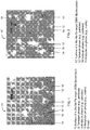
- FIG. 3A is a scanning electron micrograph (backscattered electrons) of a region of a sputter target including molybdenum, niobium and tantalum including a molybdenum phase 16 and a point 32 in the molybdenum phase.
- FIG. 3B is an illustrative energy dispersive x-ray spectrograph taken at the point 32 of FIG. 3A . The spectrograph of FIG. 3B includes only a peak 34 corresponding to molybdenum. As illustrated by FIG.
- the sputter target may include a region that includes a phase of substantially pure molybdenum (i.e., including 80 atomic % or more molybdenum, 90 atomic % or more molybdenum, or 95 atomic % or more molybdenum).
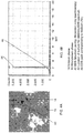
- FIG. 4A is a scanning electron micrograph (backscattered electrons) of a region of a sputter target including molybdenum, niobium and tantalum including a niobium phase 14 and a point 42 in the niobium phase.
- FIG. 4B is an illustrative energy dispersive x-ray spectrograph taken at the point 42 of FIG. 4A . The spectrograph of FIG. 4B includes only a peak 44 corresponding to niobium. As illustrated by FIG.
- the sputter target may include a region that includes a phase of substantially pure second metal element (i.e., including 80 atomic % or more of the second metal element, 90 atomic % or more of the second metal element, or 95 atomic % or more of the second metal element), such as a phase of substantially pure niobium, or a phase of substantially pure vanadium.
- a phase of substantially pure second metal element i.e., including 80 atomic % or more of the second metal element, 90 atomic % or more of the second metal element, or 95 atomic % or more of the second metal element
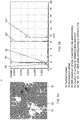
- FIG. 5A is a scanning electron micrograph (backscattered electrons) of a region of a sputter target including molybdenum, niobium and tantalum including a tantalum phase 12, a molybdenum phase 16, and a point 52 in the tantalum phase.
- FIG. 5B is an illustrative energy dispersive x-ray spectrograph taken at the point 52 of FIG. 5A . The spectrograph of FIG. 5B includes only peaks 54, 54', 54", and 54''' corresponding to tantalum. As illustrated by FIG.
- the sputter target may include a region that includes a phase of substantially pure third metal element (i.e., including 80 atomic % or more of the third metal element, 90 atomic % or more of the third metal element, or 95 atomic % or more of the third metal element), such as a phase of substantially pure tantalum, a phase of substantially pure titanium, or a phase of substantially pure chromium.
- a phase of substantially pure third metal element i.e., including 80 atomic % or more of the third metal element, 90 atomic % or more of the third metal element, or 95 atomic % or more of the third metal element
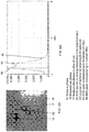
- FIG. 6A is a scanning electron micrograph (backscattered electrons) of a region of a sputter target including molybdenum, niobium and tantalum.
- the micrograph illustrates that the sputter target includes a niobium phase 14, a molybdenum phase 16, a molybdenum/niobium alloy phase 17, and a point 62 in the alloy phase 17.
- FIG. 6B is an illustrative energy dispersive x-ray spectrograph taken at the point 62 of FIG. 6A .
- the spectrograph of FIG. 6B includes both peaks 64 corresponding to Mo and 66 corresponding to Nb.
- the sputter target may include a region that includes an alloy phase including the second metal element and molybdenum, such as an alloy of niobium and molybdenum.
- FIG. 7A is a scanning electron micrograph (backscattered electrons) of a region of a sputter target including molybdenum, niobium and tantalum.
- the micrograph illustrates that the sputter target includes a tantalum phase 12, a molybdenum phase 16, a molybdenum/tantalum alloy phase 19, and a point 72 in the alloy phase 19.
- FIG. 7B is an illustrative energy dispersive x-ray spectrograph taken at the point 72 of FIG. 7A .
- the spectrograph of FIG. 7B includes both peaks 74 corresponding to Mo and 76, 76' corresponding to tantalum.
- the sputter target may include a region that includes an alloy phase including the third metal element and molybdenum, such as an alloy of tantalum and molybdenum.
- the total concentration of molybdenum in the target may be 50 atomic % or more, preferably 55 atomic % or more, more preferably 60 atomic % or more, even more preferably 63 atomic % or more, and most preferably 65 atomic % or more.
- the concentration of molybdenum in the target may be 95 atomic % or less, preferably 90 atomic % or less, more preferably 85 atomic % or less, even more preferably 83 atomic % or less, and most preferably 81 atomic % or less.
- the target includes at least two additional metal elements (i.e., a second metal element and a third metal element).
- the second metal element and the third metal element may each independently have an atomic mass greater than or less than the atomic mass of molybdenum.
- the second metal element may have an atomic mass than it less than the atomic mass of molybdenum and the third metal element may have an atomic mass that is greater than the atomic mass of molybdenum.
- the second metal element and the third metal element may both have an atomic mass less than the atomic mass of molybdenum.
- the second and third metal elements may be selected from IUPAC group 4, 5, and 6 elements.
- the target includes two or more elements (i.e., the second metal element and the third metal element) selected from the group consisting of titanium, tantalum, niobium, chromium, vanadium, hafnium, zirconium, and tungsten. More preferably the target includes two or more elements selected from the group consisting of titanium, tantalum, niobium, chromium, and vanadium.
- the second metal element of the sputter target may be an element selected from the group consisting of titanium, tantalum, niobium, chromium, and vanadium.
- the third metal element of the sputter target may be an element different from the second metal element and selected from the group consisting of titanium, tantalum, niobium, chromium, and vanadium. More preferred second metal elements include niobium and vanadium. Most preferably the second metal elements is niobium. More preferred third metal elements include an element selected from the group consisting of titanium, chromium, niobium, vanadium, and tantalum, with the proviso that the third metal element is different from the second metal element. Most preferably, the third metal element is tantalum.
- exemplary targets include targets including, consisting essentially of, or consisting of: molybdenum, niobium, and tantalum; molybdenum, niobium and chromium; molybdenum, niobium, and vanadium; molybdenum, niobium, and titanium; molybdenum, vanadium, and tantalum; molybdenum, vanadium, and chromium; molybdenum, vanadium, and titanium; molybdenum, niobium, vanadium, and chromium; molybdenum, niobium, vanadium, and tantalum; molybdenum, niobium, vanadium, and titanium; or molybdenum, niobium, vanadium, titanium and tantalum.
- Preferred targets include targets including, consisting essentially of, or consisting of: molybdenum, niobium, and tantalum; molybdenum, niobium and chromium; molybdenum, niobium, and vanadium; molybdenum, niobium, and titanium; molybdenum, vanadium, and tantalum; molybdenum, vanadium, and chromium; or molybdenum, vanadium, and titanium.
- Most preferred targets include targets including, consisting essentially of, or consisting of molybdenum, niobium, and tantalum.
- the concentration of the second metal element, the third metal element, or the combination of the second and third metal element in the sputter target may be 0.1 atomic % or more, preferably 0.5 atomic % or more, more preferably 1 atomic % or more, even more preferably 2 atomic % or more, and most preferably 5 atomic % or more, based on the total concentration of atoms in the target.
- the concentration of the second metal element, the third metal element, or the combination of the second and third metal element in the sputter target may be less than 50 atomic %, preferably 45 atomic % or less, more preferably 40 atomic % or less, even more preferably 35 atomic % or less and most preferably 30 atomic % or less, based on the total concentration of atoms in the target.
- the density of molybdenum, titanium, vanadium, chromium, niobium, and tantalum are 10.2, 4.51, 6.11, 7.15, 8.57, and 16.4 g/cm 3 , respectively.
- the density of the sputter target may be greater than 0.85 ⁇ t , preferably greater than 0.90 ⁇ t , more preferably greater than 0.92 ⁇ t , even more preferably greater than 0.94 ⁇ t , even more preferably greater than 0.96 ⁇ t , and most preferably greater than 0.98 ⁇ t .
- the density of the sputter target is preferably less than 1.00 ⁇ t .
- the texture of a sputter target may be determined by the orientation of the grains, such as the orientation of the grains of the first phase, the second phase, the third phase, or any combination thereof.
- one or more of the phases may generally be oriented with ⁇ 110>//ND, ⁇ 111>//ND, ⁇ 100>//ND, or a combination thereof.
- the rates at which the sputter target is sputtered e.g., the deposition rate of a sputtered film
- the sputter target has a generally uniform orientation.
- the orientation of the grains may be measured by electron back scattered diffraction, using the method described in U.S. Patent Application Publication No.
- the percentage of grains in a unit volume of a body centered cubic metal aligned within 15 degrees of ⁇ 110> // ND may be greater than 5%, greater than 15%, 20.4% or greater than 30%.
- the standard deviation of the texture gradient (e.g., the 100 gradient, the 111 gradient, or both) may be less than 4.0, preferably less than 2.0, more preferably less than 1.7, even more preferably less than 1.5, even more preferably less than 1.3, and most preferably less than 1.1.
- the variation in the orientation in the through-thickness direction may also be relatively low.
- through-thickness texture gradient for the texture components 100 // ND, 111 // ND, or both may be 6%/mm or less, preferably 4%/mm or less, and more preferably 2%/mm or less (as measured using the method described in International Patent Application Publication No. WO 2009/020619 A1 ).
- the sputter targets may be used to produce a structure having at least one molybdenum containing layer (e.g., a deposited layer, such as a deposited film layer) that comprises molybdenum, a second metal element, and a third metal element.
- the sputter target may be used to produce a deposited layer comprising molybdenum, a second metal element selected from niobium and vanadium, and a third metal element different from the second metal element, wherein the third metal element is selected from the group consisting of titanium, chromium, niobium, vanadium, and tantalum.
- the second metal element is niobium.
- the third metal element is tantalum.
- the second metal element is niobium and the third metal element is tantalum.
- the process of depositing a molybdenum containing layer on a substrate may include one or any combination of the following: providing a particle, such as a charged particle, accelerating a particle, or impacting a sputter target with a particle, so that atoms are removed from a sputter target and deposited onto a substrate.
- Preferred particles include atomic particles and subatomic particles.
- the subatomic particle may be an ion.
- the sputter target may be employed to deposit a molybdenum containing layer including 50 atomic % or more molybdenum, 0.5 atomic % or more of the second metal element, and 0.5 atomic % or more of the third metal element, based on the total number of atoms in the layer.
- the concentration of molybdenum in the molybdenum containing layer may be 60 atomic % or more, 65 atomic % or more, 70 atomic % or more, or 75 atomic % or more, based on the total concentration of atoms in the molybdenum containing layer.
- the concentration of molybdenum in the molybdenum containing layer may be 98 atomic % or less, preferably 95 atomic % or less, more preferably 90 atomic % or less, even more preferably 85 atomic % or less, and most preferably 83 atomic % or less, based on the total number of atoms in the molybdenum containing layer.
- the ratio of the concentration of molybdenum (in atomic %) in the deposited layer to the concentration of molybdenum in the sputter target (in atomic %) may be 0.50 or more, 0.67 or more, 0.75 or more, 0.80 or more, or 0.9 or more.
- the ratio of the concentration of molybdenum in the deposited layer to the concentration of molybdenum in the sputter target may be 2.00 or less, 1.5 or less, 1.33 or less, 1.25 or less, or 1.11 or less.
- the second metal element and the third metal element may each independently be present at a concentration 0.1 atomic % or more, preferably 1 atomic % or more, more preferably 3 atomic % or more, even more preferably greater 5 atomic % or more, and most preferably 7 atomic % or more, based on the total concentration of atoms in the molybdenum containing layer.
- the second metal element and the third metal element may each independently be present at a concentration of 40 atomic % or less, 35 atomic % or less, 30 atomic % or less, 25 atomic % or less, 20 atomic % or less, or 10 atomic % or less, based on the total concentration of atoms in the molybdenum containing layer.
- the total concentration of the second and third metal elements is preferably 5 atomic % or more, more preferably 10 atomic % or more, and most preferably 15 atomic % or more, based on the total concentration of atoms in the molybdenum containing layer.
- the total concentration of the second and third metal elements may be 20 atomic % or more, based on the total concentration of atoms in the molybdenum containing layer.
- the total of the second metal element and the third metal element may be 50 atomic % or less, 45 atomic % or less, 40 atomic % or less, 35 atomic % or less, 30 atomic % or less, or 25 atomic % or less, based on the total concentration of atoms in the molybdenum containing layer.
- the ratio of the total concentration of the second and third metal elements (in atomic %) in the deposited layer to the total concentration of the second and third metal elements in the sputter target (in atomic %) may be 0.50 or more, 0.67 or more, 0.8 or more, or 0.9 or more.
- the ratio of the total concentration of the second and third metal elements (in atomic %) in the deposit layer to the total concentration of the second and third metal elements in the sputter target (in atomic %) may be 2.00 or less, 1.5 or less, 1.25 or less, or 1.11 or less.
- the deposited molybdenum containing layer may be deposited (e.g., by a process that includes a step of sputtering the sputter target) onto a substrate.
- one aspect of the invention is a multi-layered material having at least a first deposited molybdenum containing layer including a first phase of the deposited layer having 50 atomic % or more molybdenum, 0.1 atomic % or more of the second metal element and 0.1 atomic % or more of the third metal element, wherein the second metal element is niobium or vanadium, and the third metal element is a metal element different from the second metal element and selected from the group consisting of titanium, chromium, niobium, vanadium, and tantalum.
- the first phase of the molybdenum containing layer may comprise 60 volume % or more, 70 volume % or more, 80 volume % or more, 90 volume % or more, or 95 volume % or more of the molybdenum containing layer.
- the molybdenum containing layer may be substantially entirely the first phase of the deposited layer.
- the concentration of the molybdenum, the second metal element, and the third metal element in the first phase of the deposited molybdenum containing layer may be any of the above described concentrations for the molybdenum, the second metal element, and the third metal element in the molybdenum containing layer.
- the deposited layer may have an average grain size of 5 to 10,000 nm.
- the average grain size may be measured using microscopy (e.g., scanning electron microscopy) of a surface normal to the thickness of the deposited layer.
- the size of an individual grain may be taken as the largest dimension of the grain in the plane normal to the thickness of the deposited layer.
- the deposited layer e.g., the first phase of the deposited layer
- a relatively small grain size e.g., a grain size less than the grain size of the first phase of the sputter target, the second phase of the sputter target, the third phase of the sputter target, or any combination thereof).
- the first phase of the deposited layer may have a grain size of 5 nm or more, 10 nm or more, 20 nm or more, or 50 nm or more.
- the first phase of the deposited film layer may have a grain size of 10,000 nm or less.
- the first phase of the deposited film layer has a grain size of 1000 nm or less, 500 nm or less, 200 nm or less, or 150 nm or less.
- the grains may be generally randomly oriented, the grains may be generally aligned, or any combination thereof.
- the grains may have any shape. For example, the grains may be generally elongated.
- the grains have a length to width ratio that is less than 100:1, more preferably less than 30:1, and most preferably less than 10:1.
- the deposited layer may include grains that have a generally large length to width ratio (e.g., greater than 5:1 and grains that have a generally small length to width ratio (e.g., less than 5:1, or less than 2:1).
- the grains may have a generally uniform shape, such as a shape having a length to width ratio less than 3:1, less than 2:1, or less than 1.5:1.
- FIG. 8A illustrates (without limitation) a microstructure using secondary electron scanning electron microscopy at a magnification of 50,000 of a deposited layer containing 80 atomic % molybdenum, 10 atomic % of the second metal element, and 10 atomic % of the third metal element.
- the deposited layer may be substantially a single phase.
- the thickness of the deposited molybdenum containing layer may vary depending on the functional requirements of the deposited layer. Without limitation, the thickness of the deposited layer may be 1 nm or more, 5 nm or more, 10 nm or more, 15 nm or more, 20 nm or more, 25 nm or more, 30 nm or more, or 35 nm or more. The thickness of the deposited molybdenum containing layer may be 3 ⁇ m or less. Preferably, the thickness of the deposited molybdenum containing layer is 1 ⁇ m or less, more preferably 0.5 ⁇ m or less, even more preferably 0.2 ⁇ m or less, even more preferably 100 nm or less, and most preferably 50 nm or less. Deposited layers having a thickness less than 1 nm are also contemplated.
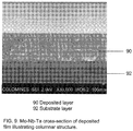
- FIG. 9 is a secondary electron scanning electron microscope micrograph (at a magnification of 10,000) of the cross-section of a deposited layer 90 containing 80 atomic % molybdenum, 10 atomic % of the second metal element, and 10 atomic % of the third metal element on a substrate 92.
- the deposited layer may include a generally columnar microstructure. Other microstructures are also contemplated.
- the arrangement of the atoms in the deposited molybdenum containing layer may be different from the arrangement of the atoms in the sputter target.
- the deposited layer may include one or more first alloy phases comprising i) at least 50 atomic % molybdenum and ii) at least one of the second metal element and the third metal element.
- the deposited layer may be substantially free of (e.g., contain less than 30 volume %, more preferably less than 10 volume %, and most preferably less than 5 volume %, based on the total volume of the deposited layer) of phases comprising greater than 90 atomic % molybdenum.
- a majority of the second metal element in the deposited layer is present in the one or more first alloy phases.
- a majority or the third metal element in the deposited layer is present in the one or more first alloy phases.
- the deposited layer may include a first phase that contains 70% or more of the molybdenum in the deposited layer, preferably 80% or more of the molybdenum in the deposited layer, more preferably 90% or more of the molybdenum in the deposited layer, and most preferably 95% or more of the molybdenum in the deposited layer.
- the deposited layer may include a first phase that further contains 70% or more of the second metal element in the deposited layer, preferably 80% or more of the second metal element in the deposited layer, more preferably 90% or more of the second metal element in the deposited layer, and most preferably 95% or more of the second metal element in the deposited layer.
- the deposited layer may include a first phase that further contains 70% or more of the third metal element in the deposited layer, preferably 80% or more of the third metal element in the deposited layer, more preferably 90% or more of the third metal element in the deposited layer, and most preferably 95% or more of the third metal element in the deposited layer.
- the deposited layer may be deposited onto a substrate using a physical vapor deposition process, such as a sputter deposition process (i.e., by sputtering).
- the deposition process may employ electric fields and/or magnetic fields (preferably both) to remove atoms or groups of atoms from the sputter target using a gas (preferably an inert gas, such as argon) and to deposit at least a portion of the removed atoms onto a substrate.
- the deposition process may employ one or more steps of heating a sputter target, one or more steps of etching a sputter target and/or substrate (for example to remove an oxide layer), one or more steps of cleaning a sputter target and/or substrate, or any combination thereof.
- the sputtering may be performed in a vacuum chamber at a pressure less than atmospheric pressure.
- the pressure, temperature, and electric fields may be chosen so that a plasma is formed.
- the process may include sputtering at one or more pressures of 100 Torr or less (13.3 kPa or less), preferably 1000 mTorr or less (133 Pa or less), more preferably 100 mTorr or less (13.3 Pa or less), and most preferably 20 mTorr or less (2.67 Pa or less).
- the process preferably includes sputtering at one or more pressures of 0.1 mTorr or more (0.0133 Pa or more), preferably 1 mTorr or more (0.133 Pa or more), and more preferably 2 mTorr or more (0.267 Pa or more).
- the deposited layer may contain one or more second alloy phases, each containing 50 atomic % or less molybdenum. If present, such optional second alloy phases preferably are present in total concentration of 40 volume % or less, more preferably 30 volume % or less, even more preferably 20 volume % or less, and most preferably 10 volume % or less, based on the total volume of the deposited layer.
- the one or more second alloy phase of the deposited layer if present, may each include at least 25 atomic % of the second metal, at least 25 atomic % of the third metal element, at least 50 atomic % of the second metal and third metal, based on the total number of atoms in the second alloy phase, or any combination thereof.
- the deposited molybdenum containing layer may function as a barrier layer, such as for performing the function of substantially or entirely avoiding the migration of atoms of an underlying layer into an overlying layer, substantially or entirely avoiding the migration of atoms of an overlying layer into an underlying layer, or both.
- the deposited molybdenum containing layer may be deposited over a first material (e.g., a first substrate material) and then have a second material deposited over it.
- the deposited molybdenum containing layer may prevent the migration (e.g., during an annealing step, during a forming step, or during use) of the one or more components (i.e., molecules or elements) of the first material into the second material, one or more components (i.e., molecules or elements) of the second material into the first material, or both.
- the molybdenum containing layer may be interposed between a substrate (e.g., a silicon substrate, or a glass substrate) and a conductive layer (such as a layer containing or consisting essentially of Cu, Al, Ag, Au, or any combination thereof).
- the thickness of the deposited molybdenum containing layer may be 1000 nm or less, 500 nm or less, 200 nm or less, 100 nm or less, or 50 nm or less.
- the thickness of the deposited molybdenum containing layer may be 1 nm or more.
- the molybdenum containing layer may include 50 atomic % or more molybdenum (e.g., 80 atomic % molybdenum), 1 atomic % or more of a second metal element (e.g., 10 atomic niobium), and 1 atomic % or more of a third metal element (e.g., 10 atomic % tantalum).
- molybdenum e.g. 80 atomic % molybdenum
- a second metal element e.g., 10 atomic niobium
- a third metal element e.g., 10 atomic % tantalum
- the materials may then be annealed, e.g., using an annealing temperature of 350°C and an annealing time of 30 minutes to determine the barrier properties of the molybdenum containing layer.
- the molybdenum containing layer may advantageously substantially if not entirely avoid the migration of components of the substrate layer into the conductive layer and/or the molybdenum containing layer, reduce or prevent the migration of components of the conductive layer into the substrate layer and/or the molybdenum containing layer, or any combination thereof.
- the molybdenum containing layer may advantageously reduce or prevent the formation of copper silicide after annealing for 30 minutes at 350°C.
- the concentration of copper silicide may be below the level detectable by x-ray diffraction methods after annealing for 30 minutes at 350°C.
- the deposited molybdenum containing layer may be employed to avoid changes in the electrical resistivity of the deposited layers (e.g., each layer, or the combination of the deposited layers) by an annealing process.
- the electrical resistivity changes by less than 30%, more preferably by less than 20%, and most preferably by less than 10%, after annealing for 30 minutes at a bout 350°C.
- Such a generally constant electrical resistivity may indicate that the molybdenum containing layer is preventing the formation of a silicide, such as copper silicide.
- the deposited layer may avoid the migration of copper atoms into a silicon layer, migration of silicon atoms into a copper layer, or both.
- concentration of copper atoms at the surface of the silicon layer may be less than 1 atomic %, preferably less than 0.1 atomic % and most preferably below the limit of detection as measured by Auger spectroscopy after annealing a structure comprising a deposition layer including molybdenum, the second metal element and the third metal element on a clean silicon wafer, deposited by sputtering the sputter target using a magnetron, the deposition layer having a thickness of 25 nm, and a layer of copper deposited over the deposition layer, the annealing at a temperature of 350°C and a time of 30 minutes.
- the concentration of silicon atoms at the surface of the copper layer may be 1 atomic % or less, preferably 0.1 atomic % or less, and most preferably below the limit of detection as measured by Auger spectroscopy
- FIG. 10A illustrates (without limitation) the Auger depth profile of a silicon substrate with a deposited molybdenum containing layer and a conductive copper layers.
- the molybdenum containing layer may be interposed between the silicon substrate and the conductive layer.
- the molybdenum containing layer may include 50 atomic % or more molybdenum (e.g., 80 atomic % molybdenum), 1 atomic % or more of a second metal element (e.g., 10 atomic niobium), and 1 atomic % or more of a third metal element (e.g., 10 atomic % tantalum).
- the materials may then be annealed, e.g., using an annealing temperature of 350°C and an annealing time of 30 minutes to determine the barrier properties of the molybdenum containing layer.
- the molybdenum containing layer may advantageously substantially if not entirely avoid the migration of silicon atoms from the substrate layer into the copper layer and/or the molybdenum containing layer, reduce or prevent the migration of copper atoms from the conductive layer into the silicon layer and/or the molybdenum containing layer, or any combination thereof.
- the molybdenum containing layer may advantageously reduce or prevent the formation of copper silicide after annealing for 30 minutes at 350°C.
- the deposited molybdenum containing layer may be characterized by one or any combination of the following: a generally good adhesion to glass (e.g., at least 2B, at least 3B, at least 4B, or at least 5B rating when tested according to ASTM B905-00), a generally good adhesion to silicon (e.g., at least 2B, at least 3B, at least 4B, or at least 5B rating when tested according to ASTM B905-00), a generally good adhesion (e.g., at least 2B, at least 3B, at least 4B, or at least 5B rating when tested according to ASTM B905-00) to a conductive layer, such as a layer containing or consisting essentially of copper, aluminum, chromium, or any combination thereof ability to prevent copper silicide formation when the molybdenum containing deposited layer (e.g., having a thickness of 200 nm or less, preferably having a thickness of 35 nm or less, and more preferably having
- the deposited molybdenum containing layer may have a relatively low electrical resistivity.
- the electrical resistivity of the molybdenum containing layer may be less than the electrical resistivity of a deposited layer of the same thickness consisting of 50 atomic % molybdenum and 50 atomic % titanium.
- the deposited molybdenum containing layer has a generally low electrical resistivity.
- the electrically resistivity (as measured by a four-point probe on a film having a thickness of 200 nm) of the deposited molybdenum containing layer preferably is of 75 ⁇ cm or less, more preferably 60 ⁇ cm or less, even more preferably 50 ⁇ cm or less, even more preferably 40 ⁇ cm or less, even more preferably 30 ⁇ cm or less, even more preferably 28 ⁇ cm or less, even more preferably 25 ⁇ cm or less, and most preferably 20 ⁇ cm or less.
- the electrically resistivity of the deposited molybdenum containing layer is 5 ⁇ cm or more. It will be appreciated that the electrical resistivity of the deposited molybdenum containing layer may also be less than 5 ⁇ cm.
- the deposited molybdenum containing layer preferably has a generally uniform electrical resistivity. For example the ratio of the standard deviation of the electrical resistivity to the average electrical resistivity (measured on a 200 nm thick layer deposited on a 76.2 mm diameter silicon wafer) preferably is 0.25 or less, more preferably 0.20 or less, even more preferably 0.12 or less, even more preferably 0.10 or less, and most preferably 0.06 or less.
- the molybdenum containing layer After depositing the molybdenum containing layer it may be desirable to at least partially etch the molybdenum containing layer.
- a step of etching may be employed so that a portion of a layer underlying the molybdenum containing layer becomes exposed (e.g., until another layer, such as a conductive layer, is deposited).
- the etch rate of the molybdenum containing layer may be generally high so that short etching times may be employed, so that milder etching chemicals may be used, so that thicker molybdenum containing layers may be employed, or any combination thereof.
- the step of etching may include a step of etching with a chemical or solution capable of removing some or all of the deposited molybdenum containing layer. More preferably, the etching step includes sufficiently etching the molybdenum layer so that a layer below the molybdenum layer, such as a substrate layer, is at least partially exposed after the etching step.
- the etching step may employ a solution or chemical that includes an acid.
- the etching step may employ a solution or chemical having a pH of 8 or more, a pH of 10 or more, or a pH of 12 or more.
- the etching step may employ a solution or chemical that includes a base.
- the etching step may employ a solution or chemical having a pH of 6 or less, a pH of 4 or less, or a pH of 2 or less.
- the etching step may employ a solution or chemical that is generally neutral.
- neutral solutions or chemicals have a pH greater than 6, a pH of 6.5 or more, a pH or 6.8 or more, or a pH of 7 or more.
- neutral solutions or chemicals also have a pH less than 8, a pH of 7.5 or less, a pH or 7.2 or less, or a pH of 7 or less.
- the etching process may employ one or more acids.
- Exemplary acids that may be used include nitric acid, sulfuric acid, hydrochloric acid, and combinations thereof.
- the etching process may employ a sulfate. Exemplary sulfates include those described in U.S. Patent No. 5,518,131 , column 2, lines 3-46 and column 2, lines 62 to column 5, line 54, such as ferric sulfate and ferric ammonium sulfate.
- the etching process may employ a solution including ferricyanide ions, chromate ions, dichromate ions, ferric ions, or any combination thereof.
- the etching process may employ one or more ions containing solutions described in U.S. Patent No. 4,747,907 , column 1, line 66 to column 8, line 2.
- a particularly preferred solution for etching the molybdenum containing layer is a solution including ferricyanide ions.
- the process of preparing the multi-layered structure includes a step of etching the molybdenum containing layer at a rate of 75 nm/min or more, more preferably 100 nm/min or more, even more preferably 150 nm/min or more, even more preferably 200 nm/min or more, even more preferably 300 nm/min or more, even more preferably 400 nm/min or more, and most preferably 500 nm/min or more.
- the etching step may employ any etching solution capable of etching the molybdenum containing layer.
- the etching step may employ a ferricyanide solution at one or more of the above rates.
- the deposited molybdenum containing layer may have a relatively high etch rate in ferricyanide solution at 25°C, such as an etch rate greater than the etch rate of a deposited layer consisting of 50 atomic % molybdenum and 50 atomic % titanium using the same etching conditions.
- the etch rate of the deposited molybdenum containing layer in ferricyanide solution at 25°C may be 75 nm/min or more, preferably 100 nm/min or more, more preferably 150 nm/min or more, even more preferably 150 nm/min or more, even more preferably 200 nm/min or more, even more preferably 300 nm/min or more, even more preferably 400 nm/min or more, and most preferably greater than 500 nm/min.
- the etch rate of the deposited molybdenum containing layer in ferricyanide solution at 25°C is preferably 10,000 nm/min or less, and most preferably 2,000 nm/min or less.
- the targets may be made using metal powder starting materials.
- One such approach includes consolidating such powders, such as by heat, pressure, or both.
- powders may be compacted and sintered, cold isostatically pressed, hot isostatically pressed, or any combination thereof.
- the process for making the target may include one or any combination of the steps disclosed by Gaydos et al. in U.S. Patent Application Publication Nos. 2007/0089984A1, published on April 26, 2007 and US2008/0314737, published on December 25, 2008 .
- the process for making the sputter targets may include a step of providing at least a first powder including 50 atomic % or more molybdenum, a second powder including 50 atomic % or more of a second metal element, and a third powder including 50 atomic % or more of a third metal element, wherein the second metal element is niobium or vanadium, and the third metal element is a different element from the second metal element and selected from the group consisting of titanium, chromium, niobium, vanadium, and tantalum.
- the individual powders e.g., the first powder, the second powder and the third powder
- the process may optionally include one or more step of consolidating the blended powder to produce a consolidated powder.
- the blending step preferably uses a temperature sufficiently low so that powder does not fuse together.
- the blending preferably uses a sufficient blending time and speed so that the first powder, the second powder, and the third powder become generally randomly distributed.
- the blending may be performed at a temperature below 100°C (e.g., at 25°C) in a V-blender.
- the process of preparing the sputter target is free of a step of mixing (e.g., mechanically mixing) two or more of the first powder, the second powder, and the third powder at a temperature at which an alloy is formed.
- the process may be free of a step of mixing two or more of the first powder, the second powder, and the third powder at a temperature of 550 °C or more, 700°C or more, 900°C or more, 1100°C or more, 1200°C or more, or 1500°C or more.
- the process may include one or more steps of encapsulating the blended powder or the consolidated powder to produce an encapsulated powder and/or one or more steps of compacting while heating the encapsulated powder to produce a first target plate.
- the process of preparing the sputter target includes one or more steps of pressing the powders or the consolidated powders to form a target plate (e.g., a block or blank) by pressing at a predetermined time, at a predetermined pressing pressure, and for a predetermined pressing temperature sufficiently high so that the powders fuse together, so that the density of the material increases to at 0.85 ⁇ t or more, where ⁇ t is the theoretical density.
- the target plate e.g., the block or blank
- target plates and methods for producing target plates are included in the teachings herein.
- the pressing step preferably includes a step of hot isostatically pressing the powder.
- the predetermined temperature is 800°C or more, more preferably 900°C or more, even more preferably 1000°C or more, even more preferably 1100°C or more, and most preferably 1200°C or more.
- the predetermined temperature is 1700°C or less, more preferably 1600°C or less, even more preferably 1500°C or less, even more preferably 1400°C or less, and most preferably 1300°C or less.
- the predetermined pressing time may be 1 minute or more, preferably 15 minutes or more, and more preferably 30 minutes or more.
- the predetermined time preferably is 24 hours or less, more preferably 12 hours or less, even more preferably 8 hours or less, and most preferably 5 hours or less.
- the predetermined pressing pressure may be 5 MPa or more, 20 MPa or more, 50 MPa or more, or 70 MPa or more.
- the predetermined pressure may be 1000 MPa or less, preferably 700 MPa or less, more preferably 400 MPa or less and most preferably 250 MPa or less.
- the process for making a target may optionally include a step of bonding (two or more target plates (e.g., a first target plate and a second target plate) to produce a bonded target plate.
- the step of bonding may be a step of edge bonding.
- the bonding process may be a diffusion bonding process.
- a bonding step may be advantageous in producing targets having a relatively large area (e.g., a length greater than 67 inches (1702 mm), or greater than 84 inches (2134 mm) and a width greater than 55 inches (1397 mm), or greater than 70 inches (1778 mm).
- a target plate formed by pressing may be capable of being rolled so that the length of the target plate is increased, so that the width of the target plate is increased, or both.
- the process of forming the sputter target may be substantially free of, or even entirely free of a step of a bonding (e.g. edge bonding) two or more target plates.
- a bonding e.g. edge bonding
- one or more steps of rolling the target plate may be employed.
- One or more steps of rolling may be advantageous in producing sputter targets having a relatively large area (e.g., a length greater than 67 inches (1702 mm), or greater than 84 inches (2134 mm) and a width greater than 55 inches (1397 mm), or greater than 70 inches (1778 mm).
- a relatively large area e.g., a length greater than 67 inches (1702 mm), or greater than 84 inches (2134 mm) and a width greater than 55 inches (1397 mm), or greater than 70 inches (1778 mm).
- the process for making the target may optionally include one or more steps of forging.
- the forging step may include hot forging (e.g., at a temperature above a recrystallization temperature of the target material). Suitable forging methods that may be used include press forging, upset forging, automatic hot forging, roll forging, precision forging, induction forging, and any combination thereof.
- the forging process may employ rotary axial forging as described for example in International Patent Application Publication No. WO2005/108639 A1 (Matera et al., published on November 17, 2005 ).
- a rotary axial forging process may employ a rotary axial forging machine such as one described in Paragraph 0032 of WO2005/108639 A1 .
- the process for making the target may include a step of tilt rolling or other asymmetric rolling, using a method or apparatus such as described in International Patent Application No. WO 2009/020619 A1 (Bozkaya et al, published on February 12, 2009 ).
- the sputter targets may be employed in producing one or more layers (e.g., as one or more barrier layers) in an electrode substrate of a flat panel display or a photovoltaic cell.
- flat panel displays which may advantageously employ the sputter targets of the present invention include a liquid crystal display (e.g., an active matrix liquid crystal display, such as a thin film transistor-liquid crystal display (i.e., a TFT-LCD)), a light emitting diode, a plasma display panel, a vacuum fluorescent display, a field emission display, an organoluminescent display, an electroluminescent displays, and an electro-chromic displays.
- a liquid crystal display e.g., an active matrix liquid crystal display, such as a thin film transistor-liquid crystal display (i.e., a TFT-LCD)
- a light emitting diode e.g., a plasma display panel, a vacuum fluorescent display, a field emission display, an organoluminescent display, an electroluminescent
- Devices that may include molybdenum containing films prepared from the sputter targets include computer monitors, optical disks, solar cells, magnetic data storage, optical communications, decorative coatings, hard coatings, glass coatings including WEB coatings, cameras, video recorders, video games, cell phones, smartphones, touch screens, global positioning satellite devices, video scoreboards, video billboards, other display panels, or the like.
- one such device may include a multi-layered structure 102.
- the multi-layered structure includes two or more layers including a substrate layer 104 and a deposited molybdenum containing layer 106.
- the substrate layer may be formed of a glass, a semiconductor, a metal, a polymer, or any combination thereof. It will be appreciated that the substrate layer may include a plurality of materials.
- a preferred substrate layers includes or consists essentially of glass.
- Another preferred substrate layer includes or consists essentially of silicon.
- the multi-layered structure includes one or more deposited layers 106.
- the deposited layer 106 may be formed by a sputter method according to the teachings herein, may be formed from a sputter target according to the teachings herein, or both.
- the deposited layer 106 may be a thin film.
- the deposited layer may have a thickness less than the thickness of the substrate layer 102.
- the deposited layer may have a thickness less than 1 ⁇ m, even more preferably less than 200 nm, even more preferably less than 100 nm, and most preferably less than 50 nm.
- the deposited layer 106 may be deposited onto the substrate 104, or the deposited layer 106 may be deposited onto one or more intermediate layers (not shown) interposed between the substrate layer 104 and the deposited layer 106.
- the multi-layered structure 102 may also include one or more conductive layers 108.
- the conductive layer 108 may have an electrical conductivity greater than the substrate layer 104, greater than the deposited layer 106, or preferably greater than both the substrate layer 104 and the deposited layer 106.
- the deposited layer 106 preferably is interposed between the substrate layer 104 and a conductive layer 108.
- a deposited layer 106 may include a first surface at least partially in contact with the substrate layer 104, and an opposing surface at least partially in contact with a conductive layer 108.
- the deposited layer 106 may be a barrier layer that reduces or prevents the diffusion of atoms between a conductive layer 108 and a substrate layer 102.
- Adhesion is measured using an adhesion tape test according to ASTM B905-00. A rating of 5B indicates good adhesion and that the deposited layer is not removed by the tape.
- Deposition rate is determined by measuring the thickness of the deposited layer (in units of nm) and dividing by the deposition time (in units of minutes).
- the etch rate (in units of ⁇ m/min) is measured as the rate of change in thickness of the deposited layer when immersed in a ferricyanide solution at 25°C.
- the sheet resistance of the deposited films is measured using a four-point probe. Two samples are measured for each deposition condition. The resistivity is then calculated by the geometry of the test sample.
- the microstructure of the deposited films is obtainable using scanning electron microscopy.
- a JEOL JSM-7000F field emission electron microscope that can measure backscattered electrons and secondary electrons is used in the examples.
- the micostructure of the sputter targets is obtainable using scanning electron microscopy.
- An ASPEX Personal Scanning Electron Micrsoscope is employed. The working distance is 20mm and the acceleration voltage is 20keV.
- the secondary electron detector is Everhart-Thornley type.
- the images are also obtained of the backscattered electrons.
- the electron microscope is also employed for measurement of energy dispersive x-ray spectroscopy using a spot size of 1 ⁇ m.
- Samples for electron microscopy of the sputter target are prepared by sectioning with an abrasive cutoff wheel, mounting the section in a polymeric material, rough grinding with SiC papers with progressively finer grits, final polishing with a diamond paste and then with an Al 2 O 3 , SiO 2 suspension.
- any numerical values recited herein include all values from the lower value to the upper value in increments of one unit provided that there is a separation of at least 2 units between any lower value and any higher value.
- the amount of a component or a value of a process variable such as, for example, temperature, pressure, time and the like is, for example, from 1 to 90, preferably from 20 to 80, more preferably from 30 to 70, it is intended that values such as 15 to 85, 22 to 68, 43 to 51, 30 to 32 etc. are expressly enumerated in this specification.
- one unit is considered to be 0.0001, 0.001, 0.01 or 0.1 as appropriate.
- Example 1 illustrates a sputter target including molybdenum, niobium and tantalum.
- Examples 2-13 illustrate deposited films prepared from the sputter target of Example 1.
- Example 1 is a sputter target that is prepared by first blending molybdenum powder having a particle size of about 3-4 ⁇ m, tantalum powder having a particle size of about 45-90 ⁇ m, and niobium powder having a particle size of about 10-45 ⁇ m to form a powder blend having about 80 atomic % molybdenum, about 10 atomic % niobium, and about 10 atomic % tantalum. The blending is done in a V-blender for about 20 minutes to obtain a homogeneous mixture of the three different powders.
- Example 1 has a density which is greater than about 94% of the theoretical density.
- the consolidated material is then removed from the can and machined to a diameter of about 58.4 mm and a thickness of about 6.4 mm.
- the target includes at least one first phase containing greater than 50 atomic % molybdenum, at least one second phase containing greater than 50 atomic % niobium, and at least one third phase containing greater than about 50 atomic % tantalum.
- a scanning electron micrograph of the sputter target using secondary electrons is illustrated in FIG. 1 .
- Scanning electron micrographs of the sputter target using backscattered electrons are illustrated in FIGs. 2 , 3A , 4A , 5A , 6A , and 7A .
- the sputter target may have a morphology including a continuous phase of molybdenum 16 a discrete phase of tantalum 12 (indicated by the light regions), and a discrete phase of niobium 14 (indicated by the dark regions).
- the sputter target is also analyzed using X-ray absorption spectroscopy for elemental analysis in different regions of the target.
- the sputter target includes a phase consisting essentially of molybdenum.
- the sputter target includes a phase that consists essentially of niobium.
- FIG. 3B the sputter target includes a phase consisting essentially of molybdenum.
- the sputter target includes a phase that consists essentially of niobium.
- the sputter target includes a region that consists essentially of tantalum. As illustrated in FIG. 6B , the sputter target includes a region that consists essentially of an alloy of molybdenum and niobium. As illustrated in FIG. 7B , the sputter target includes a region that consists essentially of an alloy of molybdenum and tantalum.
- the majority of the sputter target may be the first phase (i.e., the phase containing 50 atomic % or more molybdenum) and the first phase may be a continuous phase.
- the alloy phases e.g., the molybdenum/niobium alloy phase and the molybdenum/tantalum alloy phase
- the metal elements e.g., diffusion of the molybdenum atoms into niobium domains and into tantalum domains.
- Examples 2-13 illustrate a method that includes steps of sputtering a thin film layer using a sputter target as taught herein onto a substrate (e.g., a silicon-containing substrate, or a glass-containing substrate).
- Sputtering may be performed using a magnetron.
- sputtering will occur for about 1 to about 240 minutes (preferably about 1 to about 40 minutes), under conditions of vacuum from about 1 to about 100 mTorr pressure (preferably from about 2 to about 20 mTorr pressure), and a spacing between the substrate and the sputter target of about 5 to 300 mm (preferably about 20 to about 150 mm.
- the resulting structure will have characteristics consistent with examples 2-13 herein.
- Examples 2-13 are prepared by placing the sputter target of Example 1 into a magnetron sputter deposition chamber using the conditions described in Tables 1A and 1B.
- the substrate is either a silicon wafer (100) orientation, or Corning 1737 glass.
- the substrate Prior to deposition, the substrate is cleaned by successive rinsing in ultrasonic baths of acetone and ethyl alcohol. The substrates are then dried by blowing nitrogen gas.
- the substrates are next loaded into the deposition chamber along with the sputter target.
- the target is sputter cleaned with an argon flow of at a pressure of about 5 mTorr at 200 W DC for about 10 minutes. During the cleaning of the target, a shutter is placed in front of the target to prevent deposition onto the substrate.
- the substrate is etched by sputtering at 60 mTorr for 30 minutes to remove possible contamination on the substrate surface.
- the shutter is removed and the target material is sputtered onto a substrate using 300 W, direct current, with the substrate at 0V, grounded.
- the spacing between the substrate and the target is maintained at about 121 mm.
- Sputtering times of about 5 minutes and about 30 minutes, and chamber pressures of about 3, about 5 and about 8 mTorr are employed as shown in Tables 1A and 1B.
- Table 1A Deposition conditions using the sputter target of Example 1 target on silicon substrate.
- FIG. 8A is a secondary electron scanning electron micrograph at a magnification of about 50,000 that illustrates the surface of the deposited layer of Example 3 (deposited using a deposition pressure of about 3 mTorr and a deposition time of about 30 minutes).
- the morphology of the deposited layer consists essentially of a single alloy phase containing about 80 atomic % molybdenum, about 10 atomic % niobium and about 10 atomic % tantalum.
- the alloy of Example 3 has an average grain size of about 49 nm.
- 8B is a secondary electron scanning electron micrograph at a magnification of about 50,000 that illustrates the surface of the deposited layer of Example 7 (deposited using a deposition pressure of about 8 mTorr and a deposition time of about 30 minutes).
- the morphology of the deposited layer consists essentially of a single alloy phase containing about 80 atomic % molybdenum, about 10 atomic % niobium and about 10 atomic % tantalum. As illustrated in FIG. 8B , the alloy has an average grain size of about 62 nm.
- FIG. 9 is a secondary electron scanning electron micrograph at a magnification of about 30,000 that illustrates the cross-section of the deposited layer of Example 7.
- the deposited layer has a columnar morphology.
- the deposited layers are deposited at a deposition rate of about 33 to about 41 nm/min.
- Samples prepared with a deposition time of about 5 minutes have a thickness of about 200 nm.
- Samples prepared with a deposition time of about 30 minutes have a thickness of about 900 to about 1300 nm.
- the adhesion to the glass substrate of the Example 10 prepared at a pressure of about 5 mTorr is about 4B.
- the adhesion to the glass substrate of the Examples 8 and 12 prepared at a pressure of 3 and 8 mTorr respectively is about 5B.
- the adhesion to the silicon substrate of Example 2, 4 and 6 prepared at pressure of 3, 5 and 8 mTorr respectively is about 5B.
- the electrical resistivity of the deposited layers is given in Table 1B for Examples 8-13.
- the average electrical resistivity of the deposited layer on the glass substrate is about 19.2 ⁇ cm for the layers having a thickness from about 100 to about 200 nm and about 18.2 ⁇ cm for the samples having a thickness greater than about 0.9 ⁇ m.
- the uniformity of the electrical resistivity is measured on Example 4, by measuring the electrical resistivity at multiple locations on the 3" wafer.
- the uniformity of the electrical resistivity is the ratio of the standard deviation of the electrical resistivity to the average electrical resistivity.
- the uniformity of the electrical resistivity of Example 4 is about 0.07.
- the etch rate of the deposited layers in ferricyanide solution for Examples 3, 5, and 7 are measured at 25°C.
- the etch rates are determined by dividing the change in thickness by the etching time.
- the etch rates, in units of nm/min are given in Table 1A.
- the average etch rate for the films prepared with the Example 1 sputter target is about 478 nm/min.
- Example 14 is prepared by depositing a 35 nm molybdenum containing layer from the Example 1 sputter target onto a silicon substrate followed by the depositing of a copper (Cu) layer having a thickness of about 300 nm onto the molybdenum containing layer.
- the composition depth profile of the multilayered material is measured using Auger depth profile analysis. The sample is then annealed for 30 minutes at 350°C and the Auger depth profile analysis is repeated.
- FIG. 10A illustrates the Auger depth profile for copper (Cu), molybdenum (Mo), niobium (Nb), tantalum (Ta), oxygen (O), and silicon (Si) before annealing.
- FIG. 10B illustrates the Auger depth profile after annealing.
- FIG. 10A illustrates the Auger depth profile for copper (Cu), molybdenum (Mo), niobium (Nb), tantalum (Ta), oxygen (O), and silicon (Si) before annealing.
- FIG. 10C illustrates the Auger depth profile for Cu, Mo, Nb, Ta, O and Si, before and after the annealing near the interfaces between the molybdenum containing layer and both the silicon substrate and the copper layer.
- the composition profiles for Cu, Mo, Nb, Ta, O, and Si are about the same before and after the annealing step.
- the molybdenum containing layer acts as a barrier to reduce and/or prevent the migration of Cu into the Si substrate and Si into the Cu layer.
- X-ray analysis of the sample after annealing shows that there is no detectable copper silicide.
- the electrical resistivity of the copper layer is about 1.7 ⁇ cm before annealing and about 1.7 ⁇ cm after annealing.
- the generally constant electrical resistivity of the copper layer further indicates that the molybdenum containing layer is preventing the formation of copper silicide.
- Comparative Example 15 is a sputter target including about 50 atomic % molybdenum and about 50 atomic % titanium.
- the sputter target is prepared using the method described for Example 1, except except only titanium and molybdenum particles are used at an atomic ratio of 50:50 of Mo:Ti, the target is hot isostatically pressed at a temperature of about 1325 °C and a pressure of about 100 to about 120 MPa for about 4 hours.
- Example 16 is a 200 nm thick film deposited on a glass substrate using the method of Example 10, except the sputter target of Example 15 is used.
- the deposition rate is about 102.6 nm/min.
- the electrical resistivity of the 200 nm thick film is about 79.8 ⁇ cm.
- the adhesion of the deposited layer to glass is about 5B.
- the etch rate of the deposited layer is about 77 nm/min.
- the deposited layer has a columnar morphology.
- Example 17 illustrates a sputter target including molybdenum, titanium, and tantalum, and Examples 18-25 illustrate deposited films prepared from the sputter target.
- Example 17 is a sputter target that is prepared by first blending molybdenum powder having a particle size of about 3-4 ⁇ m, titanium powder having a particle size of about 10-45 ⁇ m, and tantalum powder having a particle size of about 45-90 ⁇ m to form a powder blend having about 80 atomic % molybdenum, about 10 atomic % titanium, and about 10 atomic % tantalum. The blending is done in a V-blender for about 20 minutes to obtain a homogeneous mixture of the three different powders.
- Example 17 has a density which is greater than about 94% of the theoretical density.
- the consolidated material is then removed from the can and machined to a diameter of about 58.4 mm and a thickness of about 6.4 mm.
- Examples 18-25 are prepared by placing the sputter target of Example 17 into a magnetron sputter deposition chamber using the conditions described in Table 2.
- the substrate is either a silicon wafer (100) orientation, or Corning 1737 glass.
- the substrate Prior to deposition, the substrate is cleaned by successive rinsing in ultrasonic baths of acetone and ethyl alcohol. The substrates are then dried by blowing nitrogen gas.
- the substrates are next loaded into the deposition chamber along with the sputter target.
- the target is sputter cleaned with an argon flow of at a pressure of about 5 mTorr at 200 W DC for about 10 minutes. During the cleaning of the target, a shutter is placed in front of the target to prevent deposition onto the substrate.
- the substrate is etched by sputtering at 60 mTorr for 30 minutes to remove possible contamination on the substrate surface.
- the shutter is removed and the target material is sputtered onto the substrate using 200 W, direct current, with the substrate at 0V, grounded.
- the spacing between the substrate and the target is maintained at about 76 mm.
- Sputtering times of 3 minutes and 30 minutes, and chamber pressures of 5 and 8 mTorr are employed as shown in Table 2. Table 2.
- the deposition rate of the Example 17 target onto the substrates is about 62.4 nm/hr using the conditions of Examples 18-25.
- the deposited films contain about 80 atomic % molybdenum, about 10 atomic % titanium and about 10 atomic % tantalum.
- the average grain size of the deposited layer of Examples 23 and 25 are measured using secondary electron scanning electron micrograph at a magnification of about 50,000 of the surface of the deposited layer.
- the average grain size of Examples 20 and 21 are 125 nm and 89 nm respectively.
- the thin films (having a thickness of about 200 nm and prepared with a deposition time of about 5 minutes) deposited by the Example 17 sputter target have an electrical resistivity of about 26.5 ⁇ cm and the thick films (having a thickness greater than about 1 ⁇ m and prepared with a deposition time of about 30 minutes) have an electrical resistivity of about 22.6 ⁇ cm.
- Example 17 When etched in ferricyanide solution at about 25°C, the deposited films form Example 17 have an average etch rate of about 61 nm/min.
- the adhesion of the deposited film to the glass substrate varied from about 2B to about 5B, and the adhesion of the deposited film to the silicon substrate is about 5B.
- the sputter target of Example 26 is prepared using the method of Example 1 except the tantalum powder is replaced with titanium powder having a particle size of about 10-45 ⁇ m.
- Deposited films are then prepared using the methods of Examples 2-13, except the sputter target including molybdenum, niobium, and titanium is employed.
- the deposited films have an etch rate of about 497 nm/min.
- the deposited films have an adhesion to glass of about 5B.
- the deposited films have an adhesion to silicon of about 5B.
- the deposited films have a grain size of about 51-98 nm.
- the deposited films have an electrical conductivity of about 30.9 ⁇ cm (for 200 nm thick films) and about 20.0 ⁇ cm (for 1 ⁇ m thick films).
- the sputter target of Example 27 is prepared using the method of Example 1 except the tantalum powder is replaced with titanium powder having a particle size of about 10-45 ⁇ m and niobium powder is replaced with vanadium powder having a particle size of about 10-45 ⁇ m.
- Deposited films are then prepared using the methods of Examples 2-13, except the sputter target including molybdenum, vanadium, and titanium is employed.
- the deposited films have an etch rate of about 270 nm/min.
- the deposited films have an adhesion to glass of about 5B.
- the deposited films have an adhesion to silicon of about 5B.
- the deposited films have a grain size of about 49-72 nm.
- the deposited films have an electrical conductivity of about 32.5 ⁇ cm (for 200 nm thick films) and about 28.5 ⁇ cm (for 1 ⁇ m thick films).
- the sputter target of Example 28 is prepared using the method of Example 1 except the niobium powder is replaced with vanadium powder having a particle size of about 10-45 ⁇ m.
- Deposited films are then prepared using the methods of Examples 2-13, except the sputter target including molybdenum, vanadium, and tantalum is employed.
- the deposited films have an etch rate of about 349 nm/min.
- the deposited films have an adhesion to glass of about 5B.
- the deposited films have an adhesion to silicon of about 0B to about 5B.
- the deposited films have a grain size of about 46-75 nm.
- the deposited films have an electrical conductivity of about 22.8 ⁇ cm (for 200 nm thick films) and about 17.5 ⁇ cm (for 1 ⁇ m thick films).
- the sputter target of Example 29 is prepared using the method of Example 1 except the tantalum powder is replaced with vanadium powder having a particle size of about 10-45 ⁇ m.
- Deposited films are then prepared using the methods of Examples 2-13, except the sputter target including molybdenum, niobium, and vanadium, is employed.
- the deposited films have an etch rate of about 243 nm/min.
- the deposited films have an adhesion to glass of about 1B to about 5B.
- the deposited films have an adhesion to silicon of about 1B to about 5B.
- the deposited films have a grain size of about 50-89 nm.
- the deposited films have an electrical conductivity of about 35.2 ⁇ cm (for 200 nm thick films) and about 33.2 ⁇ cm (for 1 ⁇ m thick films).
- the sputter target of Example 29 is prepared using the method of Example 1 except the titanium powder is replaced with chromium powder having a particle size of about 10-45 ⁇ m.
- Deposited films are then prepared using the methods of Examples 2-13, except the sputter target including molybdenum, niobium, and chromium, is employed.
- the deposited films have an etch rate of about 441 nm/min.
- the deposited films have an adhesion to glass of about 3B to about 5B.
- the deposited films have an adhesion to silicon of about 4B to about 5B.
- the deposited films have a grain size of about 45-63 nm.
- the deposited films have an electrical conductivity of about 27.9 ⁇ cm (for 200 nm thick films) and about 21.4 ⁇ cm (for 1 ⁇ m thick films).
Landscapes
- Chemical & Material Sciences (AREA)
- Engineering & Computer Science (AREA)
- Materials Engineering (AREA)
- Mechanical Engineering (AREA)
- Metallurgy (AREA)
- Organic Chemistry (AREA)
- Chemical Kinetics & Catalysis (AREA)
- General Engineering & Computer Science (AREA)
- Theoretical Computer Science (AREA)
- Inorganic Chemistry (AREA)
- Human Computer Interaction (AREA)
- Physics & Mathematics (AREA)
- General Physics & Mathematics (AREA)
- Physical Vapour Deposition (AREA)
- Electrodes Of Semiconductors (AREA)
- Electroluminescent Light Sources (AREA)
Applications Claiming Priority (2)
| Application Number | Priority Date | Filing Date | Title |
|---|---|---|---|
| US12/827,550 US8449817B2 (en) | 2010-06-30 | 2010-06-30 | Molybdenum-containing targets comprising three metal elements |
| PCT/US2010/040772 WO2012002970A1 (en) | 2010-06-30 | 2010-07-01 | Molybdenum containing targets |
Publications (2)
| Publication Number | Publication Date |
|---|---|
| EP2588636A1 EP2588636A1 (en) | 2013-05-08 |
| EP2588636B1 true EP2588636B1 (en) | 2019-03-20 |
Family
ID=42342772
Family Applications (1)
| Application Number | Title | Priority Date | Filing Date |
|---|---|---|---|
| EP10730332.3A Not-in-force EP2588636B1 (en) | 2010-06-30 | 2010-07-01 | Molybdenum containing targets |
Country Status (6)
| Country | Link |
|---|---|
| US (5) | US8449817B2 (OSRAM) |
| EP (1) | EP2588636B1 (OSRAM) |
| JP (3) | JP5751545B2 (OSRAM) |
| KR (2) | KR20140001194A (OSRAM) |
| CN (2) | CN105018889B (OSRAM) |
| WO (1) | WO2012002970A1 (OSRAM) |
Families Citing this family (28)
| Publication number | Priority date | Publication date | Assignee | Title |
|---|---|---|---|---|
| JPH0685028B2 (ja) | 1985-11-29 | 1994-10-26 | チバ―ガイギー アクチエンゲゼルシャフト | ソフトコンタクトレンズ |
| JPH0685029B2 (ja) | 1985-11-29 | 1994-10-26 | チバ―ガイギー アクチエンゲゼルシャフト | 酸素透過性ソフトコンタクトレンズの製造方法 |
| US7837929B2 (en) * | 2005-10-20 | 2010-11-23 | H.C. Starck Inc. | Methods of making molybdenum titanium sputtering plates and targets |
| US8449818B2 (en) | 2010-06-30 | 2013-05-28 | H. C. Starck, Inc. | Molybdenum containing targets |
| US8449817B2 (en) * | 2010-06-30 | 2013-05-28 | H.C. Stark, Inc. | Molybdenum-containing targets comprising three metal elements |
| WO2012154817A1 (en) | 2011-05-10 | 2012-11-15 | H.C. Starck, Inc. | Composite target |
| JP5928689B2 (ja) * | 2012-01-10 | 2016-06-01 | 大日本印刷株式会社 | タッチパネル用部材、座標検出装置、およびタッチパネル用部材の製造方法 |
| US9334565B2 (en) * | 2012-05-09 | 2016-05-10 | H.C. Starck Inc. | Multi-block sputtering target with interface portions and associated methods and articles |
| GB201307535D0 (en) * | 2013-04-26 | 2013-06-12 | Rolls Royce Plc | Alloy composition |
| AT13879U1 (de) * | 2013-10-04 | 2014-10-15 | Plansee Se | Berührungssensoranordnung |
| WO2016115026A2 (en) * | 2015-01-12 | 2016-07-21 | H.C. Starck Inc. | SPUTTERING TARGETS AND DEVICES INCLUDING Mo, Nb, AND Ta, AND METHODS |
| JP6459058B2 (ja) * | 2015-03-30 | 2019-01-30 | 日立金属株式会社 | Mo合金ターゲット |
| US9997406B2 (en) | 2016-02-04 | 2018-06-12 | International Business Machines Corporation | Columnar interconnects and method of making them |
| US9748173B1 (en) | 2016-07-06 | 2017-08-29 | International Business Machines Corporation | Hybrid interconnects and method of forming the same |
| US9875966B1 (en) | 2016-08-01 | 2018-01-23 | International Business Machines Corporation | Method and structure of forming low resistance interconnects |
| US9793156B1 (en) | 2016-09-12 | 2017-10-17 | International Business Machines Corporation | Self-aligned low resistance metallic interconnect structures |
| AT15356U1 (de) * | 2016-09-29 | 2017-07-15 | Plansee Se | Sputtering Target |
| JP6397592B1 (ja) * | 2017-10-02 | 2018-09-26 | 住友化学株式会社 | スパッタリングターゲットの製造方法およびスパッタリングターゲット |
| US10224242B1 (en) | 2017-11-14 | 2019-03-05 | International Business Machines Corporation | Low-resistivity metallic interconnect structures |
| US11220735B2 (en) * | 2018-02-08 | 2022-01-11 | Medtronic Minimed, Inc. | Methods for controlling physical vapor deposition metal film adhesion to substrates and surfaces |
| CN108273994B (zh) * | 2018-03-30 | 2024-04-19 | 江苏理成科技有限公司 | 高密度钼铌合金靶材的制备装置和方法 |
| DE102018113340B4 (de) * | 2018-06-05 | 2020-10-01 | Otto-Von-Guericke-Universität Magdeburg | Dichteoptimierte Molybdänlegierung |
| US10600686B2 (en) | 2018-06-08 | 2020-03-24 | International Business Machines Corporation | Controlling grain boundaries in high aspect-ratio conductive regions |
| CN111058003B (zh) * | 2019-11-28 | 2021-10-08 | 基迈克材料科技(苏州)有限公司 | 钼铌合金靶材及其制备方法、黑化膜 |
| CN112609162B (zh) * | 2020-12-10 | 2023-04-04 | 宁波江丰钨钼材料有限公司 | 一种lcd钼靶材及其轧制方法与应用 |
| CN114134385B (zh) * | 2021-12-03 | 2023-05-30 | 东南大学 | 一种难熔中熵合金及其制备方法 |
| EP4245871A1 (fr) * | 2022-03-18 | 2023-09-20 | Nivarox-FAR S.A. | Alliage d'or |
| CN116219384A (zh) * | 2023-03-10 | 2023-06-06 | 湘潭大学 | 一种Mo-Ti-Ta合金薄膜及其制备方法 |
Family Cites Families (116)
| Publication number | Priority date | Publication date | Assignee | Title |
|---|---|---|---|---|
| US2678269A (en) | 1951-10-06 | 1954-05-11 | Climax Molybdenum Co | Molybdenum-titanium alloys |
| US2678268A (en) * | 1951-10-06 | 1954-05-11 | Climax Molybdenum Co | Molybdenum-vanadium alloys |
| US2678270A (en) | 1951-10-06 | 1954-05-11 | Climax Molybdenum Co | Molybdenum-tantalum alloys |
| US3841846A (en) * | 1970-01-25 | 1974-10-15 | Mallory & Co Inc P R | Liquid phase sintered molybdenum base alloys having additives and shaping members made therefrom |
| US3714702A (en) | 1971-08-17 | 1973-02-06 | Atomic Energy Commission | Method for diffusion bonding refractory metals and alloys |
| DE2522690C3 (de) | 1975-05-22 | 1982-03-04 | Goetze Ag, 5093 Burscheid | Plasmaauftragsschweißpulver für die Herstellung verschleißfester Schichten |
| JPS5496775A (en) | 1978-01-17 | 1979-07-31 | Hitachi Ltd | Method of forming circuit |
| US4594219A (en) | 1985-08-02 | 1986-06-10 | Metals, Ltd. | Powder metal consolidation of multiple preforms |
| US4647426A (en) | 1985-12-23 | 1987-03-03 | Battelle Memorial Institute | Production of billet and extruded products from particulate materials |
| US4747907A (en) | 1986-10-29 | 1988-05-31 | International Business Machines Corporation | Metal etching process with etch rate enhancement |
| JPH0791636B2 (ja) | 1987-03-09 | 1995-10-04 | 日立金属株式会社 | スパツタリングタ−ゲツトおよびその製造方法 |
| JPS63241164A (ja) | 1987-03-30 | 1988-10-06 | Toshiba Corp | スパッタリングターゲットおよび電気配線用合金膜 |
| US4820393A (en) | 1987-05-11 | 1989-04-11 | Tosoh Smd, Inc. | Titanium nitride sputter targets |
| DE3718779A1 (de) | 1987-06-04 | 1988-12-22 | Krauss Maffei Ag | Schnecke od. dgl. maschinenteil fuer kunststoffverarbeitende maschinen |
| US5294321A (en) | 1988-12-21 | 1994-03-15 | Kabushiki Kaisha Toshiba | Sputtering target |
| US4931753A (en) | 1989-01-17 | 1990-06-05 | Ford Aerospace Corporation | Coplanar waveguide time delay shifter |
| US4931253A (en) | 1989-08-07 | 1990-06-05 | United States Of America As Represented By The Secretary Of The Air Force | Method for producing alpha titanium alloy pm articles |
| US4995942A (en) | 1990-04-30 | 1991-02-26 | International Business Machines Corporation | Effective near neutral pH etching solution for molybdenum or tungsten |
| JPH04333565A (ja) | 1991-01-17 | 1992-11-20 | Mitsubishi Materials Corp | スパッタリングターゲットおよびその製造方法 |
| JPH0539566A (ja) | 1991-02-19 | 1993-02-19 | Mitsubishi Materials Corp | スパツタリング用ターゲツト及びその製造方法 |
| US5292423A (en) | 1991-04-09 | 1994-03-08 | New Mexico State University Technology Transfer Corp. | Method and apparatus for trace metal testing |
| US5234487A (en) | 1991-04-15 | 1993-08-10 | Tosoh Smd, Inc. | Method of producing tungsten-titanium sputter targets and targets produced thereby |
| TW234767B (OSRAM) | 1992-09-29 | 1994-11-21 | Nippon En Kk | |
| JPH06177085A (ja) * | 1992-12-09 | 1994-06-24 | Hitachi Ltd | 配線形成方法 |
| JPH06264233A (ja) | 1993-03-12 | 1994-09-20 | Nikko Kinzoku Kk | Tft製造用スパッタリングタ−ゲット |
| US5429877A (en) | 1993-10-20 | 1995-07-04 | The United States Of America As Represented By The Secretary Of The Air Force | Internally reinforced hollow titanium alloy components |
| US5397050A (en) | 1993-10-27 | 1995-03-14 | Tosoh Smd, Inc. | Method of bonding tungsten titanium sputter targets to titanium plates and target assemblies produced thereby |
| US5693156A (en) | 1993-12-21 | 1997-12-02 | United Technologies Corporation | Oxidation resistant molybdenum alloy |
| US5518131A (en) | 1994-07-07 | 1996-05-21 | International Business Machines Corporation | Etching molydbenum with ferric sulfate and ferric ammonium sulfate |
| US5857611A (en) | 1995-08-16 | 1999-01-12 | Sony Corporation | Sputter target/backing plate assembly and method of making same |
| US6193856B1 (en) * | 1995-08-23 | 2001-02-27 | Asahi Glass Company Ltd. | Target and process for its production, and method for forming a film having a highly refractive index |
| JP3646311B2 (ja) * | 1996-02-09 | 2005-05-11 | セイコーエプソン株式会社 | 多層配線のコンタクト構造、アクティブマトリクス基板及びその製造方法 |
| US5896553A (en) | 1996-04-10 | 1999-04-20 | Sony Corporation | Single phase tungsten-titanium sputter targets and method of producing same |
| US5963778A (en) | 1997-02-13 | 1999-10-05 | Tosoh Smd, Inc. | Method for producing near net shape planar sputtering targets and an intermediate therefor |
| US6030514A (en) * | 1997-05-02 | 2000-02-29 | Sony Corporation | Method of reducing sputtering burn-in time, minimizing sputtered particulate, and target assembly therefor |
| JP3629954B2 (ja) | 1997-06-17 | 2005-03-16 | ヤマハ株式会社 | 半導体装置及びその製造方法 |
| US20030052000A1 (en) | 1997-07-11 | 2003-03-20 | Vladimir Segal | Fine grain size material, sputtering target, methods of forming, and micro-arc reduction method |
| US5895663A (en) | 1997-07-31 | 1999-04-20 | L. Perrigo Company | Pseudoephedrine hydrochloride extended-release tablets |
| JP2989169B2 (ja) | 1997-08-08 | 1999-12-13 | 日立金属株式会社 | Ni−Al系金属間化合物ターゲットおよびその製造方法ならびに磁気記録媒体 |
| US6010583A (en) | 1997-09-09 | 2000-01-04 | Sony Corporation | Method of making unreacted metal/aluminum sputter target |
| JPH1180942A (ja) | 1997-09-10 | 1999-03-26 | Japan Energy Corp | Taスパッタターゲットとその製造方法及び組立体 |
| JP4237742B2 (ja) | 1997-12-24 | 2009-03-11 | 株式会社東芝 | スパッタリングターゲットの製造方法 |
| JP4002659B2 (ja) | 1998-03-04 | 2007-11-07 | アルプス電気株式会社 | IrMn系合金成膜用ターゲット、およびそれを用いた反強磁性膜 |
| US6183686B1 (en) | 1998-08-04 | 2001-02-06 | Tosoh Smd, Inc. | Sputter target assembly having a metal-matrix-composite backing plate and methods of making same |
| US6071389A (en) | 1998-08-21 | 2000-06-06 | Tosoh Smd, Inc. | Diffusion bonded sputter target assembly and method of making |
| KR20010080499A (ko) | 1998-12-03 | 2001-08-22 | 추후제출 | 삽입체 타겟 조립체 및 그 제조 방법 |
| US6328927B1 (en) | 1998-12-24 | 2001-12-11 | Praxair Technology, Inc. | Method of making high-density, high-purity tungsten sputter targets |
| US6521108B1 (en) | 1998-12-29 | 2003-02-18 | Tosoh Smd, Inc. | Diffusion bonded sputter target assembly and method of making same |
| US20040159374A1 (en) | 1999-01-07 | 2004-08-19 | Jiin-Huey Chern Lin | Titanium alloy composition having a major phase of alpha" |
| US6726787B2 (en) | 1999-01-07 | 2004-04-27 | Jiin-Huey Chern Lin | Process for making a work piece having a major phase of α from a titanium alloy |
| JP2000239838A (ja) | 1999-02-15 | 2000-09-05 | Sony Corp | 固相拡散接合されたスパッタリングターゲット組立体およびその製造方法 |
| TWI255957B (en) | 1999-03-26 | 2006-06-01 | Hitachi Ltd | Liquid crystal display device and method of manufacturing the same |
| JP2000284326A (ja) | 1999-03-30 | 2000-10-13 | Hitachi Ltd | 液晶表示装置とその製造方法 |
| US6165413A (en) | 1999-07-08 | 2000-12-26 | Praxair S.T. Technology, Inc. | Method of making high density sputtering targets |
| US6042777A (en) | 1999-08-03 | 2000-03-28 | Sony Corporation | Manufacturing of high density intermetallic sputter targets |
| US6199747B1 (en) | 1999-08-30 | 2001-03-13 | International Business Machines Corporation | High temperature refractory joining paste |
| US6755948B1 (en) | 1999-11-22 | 2004-06-29 | Nikko Materials Company, Limited | Titanium target for sputtering |
| US6619537B1 (en) | 2000-06-12 | 2003-09-16 | Tosoh Smd, Inc. | Diffusion bonding of copper sputtering targets to backing plates using nickel alloy interlayers |
| CN1370853A (zh) | 2001-02-23 | 2002-09-25 | 光洋应用材料科技股份有限公司 | 金属溅镀靶材的制造方法 |
| DE10111269A1 (de) | 2001-03-09 | 2002-09-12 | Bosch Gmbh Robert | Sensor zur Detektion von Gasen |
| JP4432015B2 (ja) * | 2001-04-26 | 2010-03-17 | 日立金属株式会社 | 薄膜配線形成用スパッタリングターゲット |
| US20030029728A1 (en) | 2001-07-18 | 2003-02-13 | Benjamin Scharifker | Process to separate the vanadium contained in inorganic acid solutions |
| JP3748221B2 (ja) | 2001-10-23 | 2006-02-22 | 日立金属株式会社 | Mo系スパッタリング用ターゲットおよびその製造方法 |
| JP4312431B2 (ja) | 2001-11-30 | 2009-08-12 | 新日鉄マテリアルズ株式会社 | ターゲット材 |
| US6638381B2 (en) | 2001-12-18 | 2003-10-28 | The Boeing Company | Method for preparing ultra-fine grain titanium and titanium-alloy articles and articles prepared thereby |
| JP2003342720A (ja) | 2002-05-20 | 2003-12-03 | Nippon Steel Corp | スパッタリング用モリブデンターゲットの製造方法及びモリブデンターゲット |
| US6614116B1 (en) | 2002-06-04 | 2003-09-02 | Micron Technology, Inc. | Buried digit line stack and process for making same |
| US20040009087A1 (en) | 2002-07-10 | 2004-01-15 | Wuwen Yi | Physical vapor deposition targets, and methods of forming physical vapor deposition targets |
| CN1723292A (zh) | 2002-12-09 | 2006-01-18 | 霍尼韦尔国际公司 | 高纯镍/钒溅射构件和制备溅射构件的方法 |
| JP2004204253A (ja) | 2002-12-24 | 2004-07-22 | Hitachi Metals Ltd | ターゲット |
| JP4574949B2 (ja) | 2003-01-14 | 2010-11-04 | 株式会社東芝 | スパッタリングターゲットとその製造方法 |
| JP4422975B2 (ja) | 2003-04-03 | 2010-03-03 | 株式会社コベルコ科研 | スパッタリングターゲットおよびその製造方法 |
| TW586336B (en) | 2003-06-30 | 2004-05-01 | Ritdisplay Corp | Electrode substrate of flat panel display |
| JP4415303B2 (ja) | 2003-07-10 | 2010-02-17 | 日立金属株式会社 | 薄膜形成用スパッタリングターゲット |
| JP2005097697A (ja) | 2003-09-26 | 2005-04-14 | Toshiba Corp | スパッタリングターゲットとその製造方法 |
| US7336336B2 (en) | 2003-10-14 | 2008-02-26 | Lg. Philips Co. Ltd. | Thin film transistor array substrate, method of fabricating the same, liquid crystal display panel having the same and fabricating method thereof |
| JP4407243B2 (ja) | 2003-11-10 | 2010-02-03 | ソニー株式会社 | 照合処理装置とその方法 |
| KR101012491B1 (ko) | 2003-12-04 | 2011-02-08 | 엘지디스플레이 주식회사 | 액정표시장치용 어레이기판과 제조방법 |
| JP2005191361A (ja) * | 2003-12-26 | 2005-07-14 | Seiko Epson Corp | 非線形抵抗素子、電気光学装置、電気光学装置の製造方法、及び電子機器 |
| AT7187U1 (de) * | 2004-02-25 | 2004-11-25 | Plansee Ag | Verfahren zur herstellung einer molybdän-legierung |
| JP4110533B2 (ja) | 2004-02-27 | 2008-07-02 | 日立金属株式会社 | Mo系ターゲット材の製造方法 |
| US7832619B2 (en) | 2004-02-27 | 2010-11-16 | Howmet Corporation | Method of making sputtering target |
| US20050230244A1 (en) * | 2004-03-31 | 2005-10-20 | Hitachi Metals, Ltd | Sputter target material and method of producing the same |
| JP4356071B2 (ja) | 2004-03-31 | 2009-11-04 | 日立金属株式会社 | スパッタリングターゲット材およびその製造方法 |
| JP4721090B2 (ja) * | 2004-04-16 | 2011-07-13 | 日立金属株式会社 | Mo系ターゲット材の製造方法 |
| US8252126B2 (en) | 2004-05-06 | 2012-08-28 | Global Advanced Metals, Usa, Inc. | Sputter targets and methods of forming same by rotary axial forging |
| US20050279630A1 (en) | 2004-06-16 | 2005-12-22 | Dynamic Machine Works, Inc. | Tubular sputtering targets and methods of flowforming the same |
| US20060042728A1 (en) | 2004-08-31 | 2006-03-02 | Brad Lemon | Molybdenum sputtering targets |
| KR101061850B1 (ko) | 2004-09-08 | 2011-09-02 | 삼성전자주식회사 | 박막 트랜지스터 표시판 및 그 제조방법 |
| JP4596878B2 (ja) | 2004-10-14 | 2010-12-15 | キヤノン株式会社 | 構造体、電子放出素子、2次電池、電子源、画像表示装置、情報表示再生装置及びそれらの製造方法 |
| RU2418886C2 (ru) | 2005-05-05 | 2011-05-20 | Х.К. Штарк Гмбх | Способ нанесения покрытий для изготовления или восстановления мишеней распыления и анодов рентгеновских трубок |
| JP2007095197A (ja) | 2005-09-29 | 2007-04-12 | Hoya Corp | 磁気記録ディスクの製造方法、および磁気記録ディスク製造装置 |
| AT8697U1 (de) * | 2005-10-14 | 2006-11-15 | Plansee Se | Rohrtarget |
| US7837929B2 (en) * | 2005-10-20 | 2010-11-23 | H.C. Starck Inc. | Methods of making molybdenum titanium sputtering plates and targets |
| KR20070049278A (ko) | 2005-11-08 | 2007-05-11 | 삼성전자주식회사 | 배선, 이를 포함하는 박막 트랜지스터 기판과 그 제조 방법 |
| JP2007227671A (ja) | 2006-02-23 | 2007-09-06 | Rohm Co Ltd | 発光素子 |
| JP5210498B2 (ja) | 2006-04-28 | 2013-06-12 | 株式会社アルバック | 接合型スパッタリングターゲット及びその作製方法 |
| US20070289864A1 (en) | 2006-06-15 | 2007-12-20 | Zhifei Ye | Large Area Sputtering Target |
| US20080118031A1 (en) * | 2006-11-17 | 2008-05-22 | H.C. Starck Inc. | Metallic alloy for X-ray target |
| JP5426173B2 (ja) | 2007-01-12 | 2014-02-26 | 新日鉄住金マテリアルズ株式会社 | Mo系スパッタリングターゲット板,および,その製造方法 |
| US20110303535A1 (en) | 2007-05-04 | 2011-12-15 | Miller Steven A | Sputtering targets and methods of forming the same |
| US8197894B2 (en) | 2007-05-04 | 2012-06-12 | H.C. Starck Gmbh | Methods of forming sputtering targets |
| WO2009020587A1 (en) | 2007-08-06 | 2009-02-12 | H.C. Starck, Inc. | Refractory metal plates with improved uniformity of texture |
| US8250895B2 (en) | 2007-08-06 | 2012-08-28 | H.C. Starck Inc. | Methods and apparatus for controlling texture of plates and sheets by tilt rolling |
| CN101896879B (zh) * | 2007-12-14 | 2013-05-29 | 株式会社爱发科 | 触摸面板、触摸面板的制造方法 |
| JP2011523978A (ja) | 2008-04-28 | 2011-08-25 | ハー ツェー シュタルク インコーポレイテッド | モリブデン−ニオブ合金、かかる合金を含有するスパッタリングターゲット、かかるターゲットの製造方法、それから製造される薄膜、およびその使用 |
| US8043655B2 (en) | 2008-10-06 | 2011-10-25 | H.C. Starck, Inc. | Low-energy method of manufacturing bulk metallic structures with submicron grain sizes |
| US8698969B2 (en) * | 2009-03-05 | 2014-04-15 | Sharp Kabushiki Kaisha | Active matrix substrate, method for producing active matrix substrate, liquid crystal panel, method for producing liquid crystal panel, liquid crystal display device, liquid crystal display unit, and television receiver |
| CN101598989B (zh) * | 2009-07-06 | 2012-07-25 | 深圳南玻伟光导电膜有限公司 | 触摸屏引线的加工工艺 |
| US8449817B2 (en) | 2010-06-30 | 2013-05-28 | H.C. Stark, Inc. | Molybdenum-containing targets comprising three metal elements |
| US8449818B2 (en) | 2010-06-30 | 2013-05-28 | H. C. Starck, Inc. | Molybdenum containing targets |
| WO2012053818A2 (ko) * | 2010-10-19 | 2012-04-26 | 주식회사 엘지화학 | 도전성 패턴을 포함하는 터치패널 및 이의 제조방법 |
| WO2012154817A1 (en) | 2011-05-10 | 2012-11-15 | H.C. Starck, Inc. | Composite target |
| CN102321871B (zh) * | 2011-09-19 | 2013-03-20 | 基迈克材料科技(苏州)有限公司 | 热等静压生产平板显示器用钼合金溅射靶材的方法 |
| US9412568B2 (en) | 2011-09-29 | 2016-08-09 | H.C. Starck, Inc. | Large-area sputtering targets |
| US9334565B2 (en) | 2012-05-09 | 2016-05-10 | H.C. Starck Inc. | Multi-block sputtering target with interface portions and associated methods and articles |
-
2010
- 2010-06-30 US US12/827,550 patent/US8449817B2/en not_active Expired - Fee Related
- 2010-07-01 KR KR1020137002413A patent/KR20140001194A/ko not_active Ceased
- 2010-07-01 KR KR1020177015375A patent/KR20170066710A/ko not_active Ceased
- 2010-07-01 WO PCT/US2010/040772 patent/WO2012002970A1/en not_active Ceased
- 2010-07-01 JP JP2013518356A patent/JP5751545B2/ja not_active Expired - Fee Related
- 2010-07-01 EP EP10730332.3A patent/EP2588636B1/en not_active Not-in-force
- 2010-07-01 CN CN201510460313.XA patent/CN105018889B/zh not_active Expired - Fee Related
- 2010-07-01 CN CN201080068832.7A patent/CN103154307B/zh not_active Expired - Fee Related
-
2013
- 2013-04-04 US US13/856,617 patent/US9017762B2/en not_active Expired - Fee Related
-
2014
- 2014-11-07 JP JP2014227545A patent/JP5933887B2/ja not_active Expired - Fee Related
-
2015
- 2015-03-26 US US14/669,258 patent/US9945023B2/en active Active
-
2016
- 2016-05-02 JP JP2016092815A patent/JP6381142B2/ja not_active Expired - Fee Related
-
2018
- 2018-03-01 US US15/908,896 patent/US10829849B2/en not_active Expired - Fee Related
-
2020
- 2020-09-30 US US17/038,325 patent/US11753702B2/en active Active
Non-Patent Citations (1)
| Title |
|---|
| None * |
Also Published As
| Publication number | Publication date |
|---|---|
| JP5751545B2 (ja) | 2015-07-22 |
| WO2012002970A1 (en) | 2012-01-05 |
| US10829849B2 (en) | 2020-11-10 |
| US20180187297A1 (en) | 2018-07-05 |
| KR20140001194A (ko) | 2014-01-06 |
| CN103154307A (zh) | 2013-06-12 |
| CN105018889B (zh) | 2018-04-06 |
| US9945023B2 (en) | 2018-04-17 |
| US20140102880A1 (en) | 2014-04-17 |
| JP2013535571A (ja) | 2013-09-12 |
| EP2588636A1 (en) | 2013-05-08 |
| KR20170066710A (ko) | 2017-06-14 |
| US9017762B2 (en) | 2015-04-28 |
| US20210079512A1 (en) | 2021-03-18 |
| US20150197845A1 (en) | 2015-07-16 |
| CN105018889A (zh) | 2015-11-04 |
| JP6381142B2 (ja) | 2018-08-29 |
| US8449817B2 (en) | 2013-05-28 |
| JP5933887B2 (ja) | 2016-06-15 |
| US20120003486A1 (en) | 2012-01-05 |
| CN103154307B (zh) | 2015-09-09 |
| JP2016194159A (ja) | 2016-11-17 |
| US11753702B2 (en) | 2023-09-12 |
| JP2015061952A (ja) | 2015-04-02 |
Similar Documents
| Publication | Publication Date | Title |
|---|---|---|
| US11753702B2 (en) | Molybdenum containing targets | |
| US10403483B2 (en) | Molybdenum containing targets | |
| JP2013535571A5 (ja) | モリブデンを含有したターゲット | |
| JPWO1995016797A1 (ja) | 配線形成用Mo−W材、配線形成用Mo−Wターゲットとその製造方法、およびMo−W配線薄膜 | |
| KR20100084668A (ko) | 내화성 금속으로 도핑된 스퍼터링 타겟 |
Legal Events
| Date | Code | Title | Description |
|---|---|---|---|
| PUAI | Public reference made under article 153(3) epc to a published international application that has entered the european phase |
Free format text: ORIGINAL CODE: 0009012 |
|
| 17P | Request for examination filed |
Effective date: 20130130 |
|
| AK | Designated contracting states |
Kind code of ref document: A1 Designated state(s): AL AT BE BG CH CY CZ DE DK EE ES FI FR GB GR HR HU IE IS IT LI LT LU LV MC MK MT NL NO PL PT RO SE SI SK SM TR |
|
| DAX | Request for extension of the european patent (deleted) | ||
| 17Q | First examination report despatched |
Effective date: 20131014 |
|
| STAA | Information on the status of an ep patent application or granted ep patent |
Free format text: STATUS: EXAMINATION IS IN PROGRESS |
|
| GRAP | Despatch of communication of intention to grant a patent |
Free format text: ORIGINAL CODE: EPIDOSNIGR1 |
|
| STAA | Information on the status of an ep patent application or granted ep patent |
Free format text: STATUS: GRANT OF PATENT IS INTENDED |
|
| INTG | Intention to grant announced |
Effective date: 20180905 |
|
| GRAS | Grant fee paid |
Free format text: ORIGINAL CODE: EPIDOSNIGR3 |
|
| GRAA | (expected) grant |
Free format text: ORIGINAL CODE: 0009210 |
|
| STAA | Information on the status of an ep patent application or granted ep patent |
Free format text: STATUS: THE PATENT HAS BEEN GRANTED |
|
| AK | Designated contracting states |
Kind code of ref document: B1 Designated state(s): AL AT BE BG CH CY CZ DE DK EE ES FI FR GB GR HR HU IE IS IT LI LT LU LV MC MK MT NL NO PL PT RO SE SI SK SM TR |
|
| REG | Reference to a national code |
Ref country code: GB Ref legal event code: FG4D |
|
| REG | Reference to a national code |
Ref country code: CH Ref legal event code: EP |
|
| REG | Reference to a national code |
Ref country code: DE Ref legal event code: R096 Ref document number: 602010057674 Country of ref document: DE |
|
| REG | Reference to a national code |
Ref country code: AT Ref legal event code: REF Ref document number: 1110610 Country of ref document: AT Kind code of ref document: T Effective date: 20190415 |
|
| REG | Reference to a national code |
Ref country code: IE Ref legal event code: FG4D |
|
| REG | Reference to a national code |
Ref country code: NL Ref legal event code: MP Effective date: 20190320 |
|
| PG25 | Lapsed in a contracting state [announced via postgrant information from national office to epo] |
Ref country code: NO Free format text: LAPSE BECAUSE OF FAILURE TO SUBMIT A TRANSLATION OF THE DESCRIPTION OR TO PAY THE FEE WITHIN THE PRESCRIBED TIME-LIMIT Effective date: 20190620 Ref country code: FI Free format text: LAPSE BECAUSE OF FAILURE TO SUBMIT A TRANSLATION OF THE DESCRIPTION OR TO PAY THE FEE WITHIN THE PRESCRIBED TIME-LIMIT Effective date: 20190320 Ref country code: SE Free format text: LAPSE BECAUSE OF FAILURE TO SUBMIT A TRANSLATION OF THE DESCRIPTION OR TO PAY THE FEE WITHIN THE PRESCRIBED TIME-LIMIT Effective date: 20190320 Ref country code: LT Free format text: LAPSE BECAUSE OF FAILURE TO SUBMIT A TRANSLATION OF THE DESCRIPTION OR TO PAY THE FEE WITHIN THE PRESCRIBED TIME-LIMIT Effective date: 20190320 |
|
| REG | Reference to a national code |
Ref country code: LT Ref legal event code: MG4D |
|
| PG25 | Lapsed in a contracting state [announced via postgrant information from national office to epo] |
Ref country code: HR Free format text: LAPSE BECAUSE OF FAILURE TO SUBMIT A TRANSLATION OF THE DESCRIPTION OR TO PAY THE FEE WITHIN THE PRESCRIBED TIME-LIMIT Effective date: 20190320 Ref country code: LV Free format text: LAPSE BECAUSE OF FAILURE TO SUBMIT A TRANSLATION OF THE DESCRIPTION OR TO PAY THE FEE WITHIN THE PRESCRIBED TIME-LIMIT Effective date: 20190320 Ref country code: NL Free format text: LAPSE BECAUSE OF FAILURE TO SUBMIT A TRANSLATION OF THE DESCRIPTION OR TO PAY THE FEE WITHIN THE PRESCRIBED TIME-LIMIT Effective date: 20190320 Ref country code: GR Free format text: LAPSE BECAUSE OF FAILURE TO SUBMIT A TRANSLATION OF THE DESCRIPTION OR TO PAY THE FEE WITHIN THE PRESCRIBED TIME-LIMIT Effective date: 20190621 Ref country code: BG Free format text: LAPSE BECAUSE OF FAILURE TO SUBMIT A TRANSLATION OF THE DESCRIPTION OR TO PAY THE FEE WITHIN THE PRESCRIBED TIME-LIMIT Effective date: 20190620 |
|
| PG25 | Lapsed in a contracting state [announced via postgrant information from national office to epo] |
Ref country code: EE Free format text: LAPSE BECAUSE OF FAILURE TO SUBMIT A TRANSLATION OF THE DESCRIPTION OR TO PAY THE FEE WITHIN THE PRESCRIBED TIME-LIMIT Effective date: 20190320 Ref country code: RO Free format text: LAPSE BECAUSE OF FAILURE TO SUBMIT A TRANSLATION OF THE DESCRIPTION OR TO PAY THE FEE WITHIN THE PRESCRIBED TIME-LIMIT Effective date: 20190320 Ref country code: IT Free format text: LAPSE BECAUSE OF FAILURE TO SUBMIT A TRANSLATION OF THE DESCRIPTION OR TO PAY THE FEE WITHIN THE PRESCRIBED TIME-LIMIT Effective date: 20190320 Ref country code: CZ Free format text: LAPSE BECAUSE OF FAILURE TO SUBMIT A TRANSLATION OF THE DESCRIPTION OR TO PAY THE FEE WITHIN THE PRESCRIBED TIME-LIMIT Effective date: 20190320 Ref country code: ES Free format text: LAPSE BECAUSE OF FAILURE TO SUBMIT A TRANSLATION OF THE DESCRIPTION OR TO PAY THE FEE WITHIN THE PRESCRIBED TIME-LIMIT Effective date: 20190320 Ref country code: PT Free format text: LAPSE BECAUSE OF FAILURE TO SUBMIT A TRANSLATION OF THE DESCRIPTION OR TO PAY THE FEE WITHIN THE PRESCRIBED TIME-LIMIT Effective date: 20190720 Ref country code: AL Free format text: LAPSE BECAUSE OF FAILURE TO SUBMIT A TRANSLATION OF THE DESCRIPTION OR TO PAY THE FEE WITHIN THE PRESCRIBED TIME-LIMIT Effective date: 20190320 Ref country code: SK Free format text: LAPSE BECAUSE OF FAILURE TO SUBMIT A TRANSLATION OF THE DESCRIPTION OR TO PAY THE FEE WITHIN THE PRESCRIBED TIME-LIMIT Effective date: 20190320 |
|
| PG25 | Lapsed in a contracting state [announced via postgrant information from national office to epo] |
Ref country code: PL Free format text: LAPSE BECAUSE OF FAILURE TO SUBMIT A TRANSLATION OF THE DESCRIPTION OR TO PAY THE FEE WITHIN THE PRESCRIBED TIME-LIMIT Effective date: 20190320 Ref country code: SM Free format text: LAPSE BECAUSE OF FAILURE TO SUBMIT A TRANSLATION OF THE DESCRIPTION OR TO PAY THE FEE WITHIN THE PRESCRIBED TIME-LIMIT Effective date: 20190320 |
|
| PG25 | Lapsed in a contracting state [announced via postgrant information from national office to epo] |
Ref country code: IS Free format text: LAPSE BECAUSE OF FAILURE TO SUBMIT A TRANSLATION OF THE DESCRIPTION OR TO PAY THE FEE WITHIN THE PRESCRIBED TIME-LIMIT Effective date: 20190720 |
|
| REG | Reference to a national code |
Ref country code: DE Ref legal event code: R097 Ref document number: 602010057674 Country of ref document: DE |
|
| PLBE | No opposition filed within time limit |
Free format text: ORIGINAL CODE: 0009261 |
|
| STAA | Information on the status of an ep patent application or granted ep patent |
Free format text: STATUS: NO OPPOSITION FILED WITHIN TIME LIMIT |
|
| PG25 | Lapsed in a contracting state [announced via postgrant information from national office to epo] |
Ref country code: DK Free format text: LAPSE BECAUSE OF FAILURE TO SUBMIT A TRANSLATION OF THE DESCRIPTION OR TO PAY THE FEE WITHIN THE PRESCRIBED TIME-LIMIT Effective date: 20190320 |
|
| 26N | No opposition filed |
Effective date: 20200102 |
|
| PG25 | Lapsed in a contracting state [announced via postgrant information from national office to epo] |
Ref country code: SI Free format text: LAPSE BECAUSE OF FAILURE TO SUBMIT A TRANSLATION OF THE DESCRIPTION OR TO PAY THE FEE WITHIN THE PRESCRIBED TIME-LIMIT Effective date: 20190320 Ref country code: MC Free format text: LAPSE BECAUSE OF FAILURE TO SUBMIT A TRANSLATION OF THE DESCRIPTION OR TO PAY THE FEE WITHIN THE PRESCRIBED TIME-LIMIT Effective date: 20190320 |
|
| REG | Reference to a national code |
Ref country code: CH Ref legal event code: PL |
|
| GBPC | Gb: european patent ceased through non-payment of renewal fee |
Effective date: 20190701 |
|
| PG25 | Lapsed in a contracting state [announced via postgrant information from national office to epo] |
Ref country code: TR Free format text: LAPSE BECAUSE OF FAILURE TO SUBMIT A TRANSLATION OF THE DESCRIPTION OR TO PAY THE FEE WITHIN THE PRESCRIBED TIME-LIMIT Effective date: 20190320 |
|
| REG | Reference to a national code |
Ref country code: BE Ref legal event code: MM Effective date: 20190731 |
|
| PG25 | Lapsed in a contracting state [announced via postgrant information from national office to epo] |
Ref country code: GB Free format text: LAPSE BECAUSE OF NON-PAYMENT OF DUE FEES Effective date: 20190701 |
|
| PG25 | Lapsed in a contracting state [announced via postgrant information from national office to epo] |
Ref country code: CH Free format text: LAPSE BECAUSE OF NON-PAYMENT OF DUE FEES Effective date: 20190731 Ref country code: LI Free format text: LAPSE BECAUSE OF NON-PAYMENT OF DUE FEES Effective date: 20190731 Ref country code: LU Free format text: LAPSE BECAUSE OF NON-PAYMENT OF DUE FEES Effective date: 20190701 Ref country code: BE Free format text: LAPSE BECAUSE OF NON-PAYMENT OF DUE FEES Effective date: 20190731 |
|
| PG25 | Lapsed in a contracting state [announced via postgrant information from national office to epo] |
Ref country code: FR Free format text: LAPSE BECAUSE OF NON-PAYMENT OF DUE FEES Effective date: 20190731 |
|
| PG25 | Lapsed in a contracting state [announced via postgrant information from national office to epo] |
Ref country code: IE Free format text: LAPSE BECAUSE OF NON-PAYMENT OF DUE FEES Effective date: 20190701 |
|
| PG25 | Lapsed in a contracting state [announced via postgrant information from national office to epo] |
Ref country code: CY Free format text: LAPSE BECAUSE OF FAILURE TO SUBMIT A TRANSLATION OF THE DESCRIPTION OR TO PAY THE FEE WITHIN THE PRESCRIBED TIME-LIMIT Effective date: 20190320 |
|
| PG25 | Lapsed in a contracting state [announced via postgrant information from national office to epo] |
Ref country code: HU Free format text: LAPSE BECAUSE OF FAILURE TO SUBMIT A TRANSLATION OF THE DESCRIPTION OR TO PAY THE FEE WITHIN THE PRESCRIBED TIME-LIMIT; INVALID AB INITIO Effective date: 20100701 Ref country code: MT Free format text: LAPSE BECAUSE OF FAILURE TO SUBMIT A TRANSLATION OF THE DESCRIPTION OR TO PAY THE FEE WITHIN THE PRESCRIBED TIME-LIMIT Effective date: 20190320 |
|
| PGFP | Annual fee paid to national office [announced via postgrant information from national office to epo] |
Ref country code: AT Payment date: 20210625 Year of fee payment: 12 |
|
| PG25 | Lapsed in a contracting state [announced via postgrant information from national office to epo] |
Ref country code: MK Free format text: LAPSE BECAUSE OF FAILURE TO SUBMIT A TRANSLATION OF THE DESCRIPTION OR TO PAY THE FEE WITHIN THE PRESCRIBED TIME-LIMIT Effective date: 20190320 |
|
| PGFP | Annual fee paid to national office [announced via postgrant information from national office to epo] |
Ref country code: DE Payment date: 20220531 Year of fee payment: 13 |
|
| REG | Reference to a national code |
Ref country code: AT Ref legal event code: MM01 Ref document number: 1110610 Country of ref document: AT Kind code of ref document: T Effective date: 20220701 |
|
| PG25 | Lapsed in a contracting state [announced via postgrant information from national office to epo] |
Ref country code: AT Free format text: LAPSE BECAUSE OF NON-PAYMENT OF DUE FEES Effective date: 20220701 |
|
| REG | Reference to a national code |
Ref country code: AT Ref legal event code: UEP Ref document number: 1110610 Country of ref document: AT Kind code of ref document: T Effective date: 20190320 |
|
| REG | Reference to a national code |
Ref country code: DE Ref legal event code: R119 Ref document number: 602010057674 Country of ref document: DE |
|
| PG25 | Lapsed in a contracting state [announced via postgrant information from national office to epo] |
Ref country code: DE Free format text: LAPSE BECAUSE OF NON-PAYMENT OF DUE FEES Effective date: 20240201 |