EP2575256A1 - Elektronische Schaltung - Google Patents
Elektronische Schaltung Download PDFInfo
- Publication number
- EP2575256A1 EP2575256A1 EP12006703A EP12006703A EP2575256A1 EP 2575256 A1 EP2575256 A1 EP 2575256A1 EP 12006703 A EP12006703 A EP 12006703A EP 12006703 A EP12006703 A EP 12006703A EP 2575256 A1 EP2575256 A1 EP 2575256A1
- Authority
- EP
- European Patent Office
- Prior art keywords
- circuit
- signal
- reset
- reset signal
- noise
- Prior art date
- Legal status (The legal status is an assumption and is not a legal conclusion. Google has not performed a legal analysis and makes no representation as to the accuracy of the status listed.)
- Granted
Links
Images

Classifications
-
- H—ELECTRICITY
- H03—ELECTRONIC CIRCUITRY
- H03K—PULSE TECHNIQUE
- H03K17/00—Electronic switching or gating, i.e. not by contact-making and –breaking
- H03K17/22—Modifications for ensuring a predetermined initial state when the supply voltage has been applied
- H03K17/223—Modifications for ensuring a predetermined initial state when the supply voltage has been applied in field-effect transistor switches
-
- H—ELECTRICITY
- H03—ELECTRONIC CIRCUITRY
- H03K—PULSE TECHNIQUE
- H03K5/00—Manipulating of pulses not covered by one of the other main groups of this subclass
- H03K5/125—Discriminating pulses
- H03K5/1252—Suppression or limitation of noise or interference
Definitions
- the present disclosure relates to electronic circuits.
- a power-on reset is used to initialize a digital circuit in an electronic device when it is powered on.
- the power-on reset for example, when the electronic device is powered on, the electronic device is initialized by supplying a reset signal to the digital circuit with a delay from the time when it is powered on.
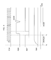
- Fig. 3 shows a circuit diagram which indicates an example of an electronic circuit in which a digital circuit is asynchronously reset by a power-on reset.
- Fig. 4 shows a timing chart which indicates an example of a clock signal, a power-on reset signal, and a status of an output terminal in the electronic circuit shown in Fig. 3 .
- a clock generator circuit 2 and a power-on reset circuit 3 are connected to an IC (Integrated Circuit) chip 101.
- a clock signal CLK is inputted from the clock generator circuit 2 to a CLK terminal of the IC chip 101, and a power-on reset signal POR is inputted from the power-on reset circuit 3 to a POR terminal of the IC chip 101.
- the IC chip 101 includes a digital circuit 111, and an output signal of the digital circuit 111 is applied to an output terminal TAR via an output buffer 112.
- a noise eliminating circuit 113 eliminates noise in the power-on reset signal.
- the noise eliminating circuit 113 Into the noise eliminating circuit 113, the clock signal CLK is supplied via an input buffer 114, and the power-on reset signal POR is supplied via an input buffer 115; and an output signal thereof in which noise has been eliminated (a reset signal RST) is used for an asynchronous reset of the digital circuit 111.
- the noise eliminating circuit 113 delays the power-on reset signal by a predetermined number of clocks, eliminates noise in the power-on reset signal by performing a logical operation between the delayed power-on reset signal and the current power-on reset signal, and outputs a signal obtained by the logical operation as the reset signal RST. Therefore, even if noise occurs in the power-on reset signal, the digital circuit 111 is not reset due to the noise.
- a delay period until a reset status due to the power-on reset signal is released and the reset signal RST is supplied to the digital circuit 111 i.e. a period from the power-on timing To to the time T1 in Fig. 4
- the value of the output signal of the digital circuit is invalid (i.e. indefinite). Therefore, during this period, a circuit or device connected to the output terminal TAR may malfunction.
- control signal for a motor is outputted from the output terminal TAR, upon a power-on, during the period when the value of the output signal of the digital circuit 111 is invalid (i.e. indefinite), the control signal may take an unexpected value and the motor runs unexpectedly.
- An electronic circuit includes a noise eliminating circuit configured to eliminate noise in a reset signal and output a signal obtained by eliminating the noise in the reset signal; a digital circuit configured to be reset by the signal outputted from the noise eliminating circuit; and an early-initialization circuit configured to fix an output signal of the digital circuit at a predetermined value until a reset status due to the reset signal is released.
- the output signal of the digital circuit does not take an invalid value during a period until a reset status, for example, due to a power-on reset signal is released, and consequently, it reduces malfunction due to the reset during an initialization of the digital circuit.
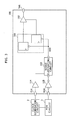
- Fig. 1 shows a circuit diagram which indicates a configuration of an electronic circuit according to an embodiment of the present disclosure.
- a clock generator circuit 2 and a power-on reset circuit 3 are connected to an IC chip 1.
- a clock signal CLK is inputted from the clock generator circuit 2 to a CLK terminal of the IC chip 1
- a power-on reset signal POR is inputted from the power-on reset circuit 3 to a POR terminal of the IC chip 1.
- An output terminal TAR of the IC chip 1 is connected to an unshown circuit or device.
- the IC chip 1 includes a digital circuit 11, an output buffer 12, a noise eliminating circuit 13, input buffers 14 and 15, and an early-initialization circuit 16.
- the digital circuit 11 is a sequential logic circuit which includes flip-flops 21 and 22. It should be noted that the digital circuit 11 may include elements other than the flip-flops 21 and 22, but they are not shown in Fig. 1 .
- the noise eliminating circuit 13 Into the noise eliminating circuit 13, the clock signal CLK is supplied via an input buffer 14, and the power-on reset signal POR is supplied via an input buffer 15; and an output signal thereof in which noise has been eliminated (a reset signal RST) is used for an asynchronous reset of the digital circuit 11.
- the noise eliminating circuit 13 delays the power-on reset signal by a predetermined number of clocks, eliminates noise in the power-on reset signal by performing a logical operation between the delayed power-on reset signal and the current power-on reset signal, and outputs a signal obtained by the logical operation as the reset signal RST to the digital circuit 11. Therefore, a period in which a reset status remains due to the power-on reset signal is set longer than the delay at the noise eliminating circuit 13.
- the early-initialization circuit 16 is put between the digital circuit 11 and the output buffer 12 connected to the output terminal TAR, fixes an output signal of the digital circuit 11 at a predetermined value until a reset status due to the power-on reset signal is released, and directly supplies an output signal of the digital circuit 11 to the output buffer 12 after the reset status due to the power-on reset signal is released.
- the digital circuit 11 outputs two output signals from the flip-flops 21 and 22.
- the early-initialization circuit 16 includes two OR operation circuits 31 and 32, performs logical operations between the respective output signals of the digital circuit 11 and the power-on reset signal, and outputs results of the logical operations.
- the value of the power-on reset signal changes to the H (high) level after the reset status is released, and this power-on reset signal is inverted and inputted as respective ones of input signals to the OR operation circuits 31 and 32.
- both of the other input and the output of the OR operation circuit 31 are set as either inverse ones or non-inverse ones
- both of the other input and the output of the OR operation circuit 32 are set as either inverse ones or non-inverse ones.
- AND operation circuits may be used instead of the OR operation circuits 31 and 32. If the AND operation circuits are used, two inputs and one output of the AND operation circuits are properly set as either inverse ones or non-inverse ones.
- the output buffer 12 is a tristate buffer. Into the output buffer 12, an input signal is supplied from the OR operation circuit 31, and a control signal is supplied from the OR operation circuit 32.
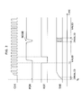
- Fig. 2 shows a timing chart which indicates an example of a clock signal, a power-on reset signal, and a status of an output terminal in the electronic circuit shown in Fig. 1 .
- the clock generator circuit 2 starts outputting the-clock-signal CLK with a delay from the power-on (the time To).
- the power-on reset circuit 3 releases a reset status set by a power-on reset signal POR .
- the reset status is released by changing the power-on reset signal POR from the L (low) level to the H (high) level.
- the clock signal CLK and the power-on reset signal POR are supplied to the noise eliminating circuit 13 of the IC chip 1.
- the noise eliminating circuit 13 delays the power-on reset signal by a predetermined number of clocks in the clock signal CLK, and supplies a reset signal RST (here, an L-level pulse signal) when both of the current power-on reset signal and the delayed power-on reset signal take the L level.
- a reset signal RST here, an L-level pulse signal
- the value of the output signal of the digital circuit 11 is invalid (indefinite).
- the digital circuit 11 is initialized, and afterward, the value of the output signal of the digital circuit 11 is valid.
- the power-on reset signal takes the L level during the period from the time To to the time T1 (i.e. the period when the output of the digital circuit 11 is indefinite)
- the fixed values outputted from the early-initialization circuit 16 are supplied to the output buffer 12, and a signal with the level specified by the early-initialization circuit 16 is supplied from the output buffer 12 to the output terminal TAR. Therefore, the level of the output terminal TAR is valid during the period from the time To to the time T1.
- the power supply still takes a low voltage, and therefore, does not ensure that the input buffer 15, the early-initialization circuit 16, and the output buffer 12 operate properly, and consequently, the level of the output terminal TAR is not valid.
- the power-on reset signal takes the H level, and therefore, the early-initialization circuit 16 directly supplies the output signal of the digital circuit 11 to the output buffer 12, and consequently, a signal with the level specified by the digital circuit 11 is applied to the output terminal TAR. During this period, the level of the output terminal TAR is also valid.
- the noise eliminating circuit 13 eliminates noise in the power-on reset signal and outputs a signal obtained by eliminating noise in the power-on reset signal; the digital circuit 11 is reset by the signal outputted from the noise eliminating circuit 13; and the early-initialization circuit 16 fixes an output signal of the digital circuit 11 at a predetermined value until a reset status due to the power-on reset signal is released.
- the output signal of the digital circuit 11 does not take an invalid value during a period until the reset status due to the power-on reset signal is released, and consequently, it reduces malfunction due to the reset during an initialization of the digital circuit 11.
- a forced reset signal generated in correspondence with a user's reset operation or the like may be used instead of the power-on reset signal. If the forced reset signal is used, a forced reset circuit which generates the forced reset signal is used instead of the power-on reset circuit 3.
- the signal inputted to the output buffer 12 connected to the output terminal TAR is made valid in an early time.
- a control signal inputted to an input buffer (e.g. tristate buffer) connected to the input terminal may be made valid in an early time.
- a signal inputted to an input/output buffer connected to the output terminal TAR may be made valid in an early time.
Landscapes
- Physics & Mathematics (AREA)
- Nonlinear Science (AREA)
- Electronic Switches (AREA)
- Logic Circuits (AREA)
- Manipulation Of Pulses (AREA)
Applications Claiming Priority (1)
| Application Number | Priority Date | Filing Date | Title |
|---|---|---|---|
| JP2011216033A JP5501320B2 (ja) | 2011-09-30 | 2011-09-30 | 電子回路 |
Publications (2)
| Publication Number | Publication Date |
|---|---|
| EP2575256A1 true EP2575256A1 (de) | 2013-04-03 |
| EP2575256B1 EP2575256B1 (de) | 2016-01-20 |
Family
ID=47048921
Family Applications (1)
| Application Number | Title | Priority Date | Filing Date |
|---|---|---|---|
| EP12006703.8A Not-in-force EP2575256B1 (de) | 2011-09-30 | 2012-09-25 | Elektronische Schaltung |
Country Status (4)
| Country | Link |
|---|---|
| US (1) | US8729934B2 (de) |
| EP (1) | EP2575256B1 (de) |
| JP (1) | JP5501320B2 (de) |
| CN (1) | CN103036545B (de) |
Families Citing this family (5)
| Publication number | Priority date | Publication date | Assignee | Title |
|---|---|---|---|---|
| JP5706455B2 (ja) * | 2013-02-19 | 2015-04-22 | Necエンジニアリング株式会社 | 制御回路、回路システム、および、制御方法 |
| CN106301300B (zh) * | 2016-08-02 | 2019-04-05 | 芯启源(上海)半导体科技有限公司 | 具有安全复位功能的脉冲同步电路及处理器 |
| JP6661585B2 (ja) | 2017-09-26 | 2020-03-11 | キヤノン株式会社 | 情報処理装置 |
| JP7074699B2 (ja) * | 2019-02-28 | 2022-05-24 | ファナック株式会社 | グリッチ除去回路及び電子装置 |
| CN113792509B (zh) * | 2021-11-16 | 2022-02-18 | 苏州浪潮智能科技有限公司 | 一种复位信号平衡方法和装置 |
Citations (3)
| Publication number | Priority date | Publication date | Assignee | Title |
|---|---|---|---|---|
| US5629642A (en) * | 1995-08-18 | 1997-05-13 | Mitsubishi Denki Kabushiki Kaisha | Power supply monitor |
| US20060103436A1 (en) * | 2004-11-17 | 2006-05-18 | Fujitsu Limited | Reset control circuit and reset control method |
| US20060214650A1 (en) * | 2003-08-22 | 2006-09-28 | Kenichi Hirooka | Semiconductor integrated circuit device and power supply voltage monitor system employing it |
Family Cites Families (12)
| Publication number | Priority date | Publication date | Assignee | Title |
|---|---|---|---|---|
| US4438357A (en) * | 1982-06-17 | 1984-03-20 | Baxter Travenol Laboratories, Inc. | Level sensitive reset circuit for digital logic |
| US4940904A (en) * | 1988-05-23 | 1990-07-10 | Industrial Technology Research Institute | Output circuit for producing positive and negative pulses at a single output terminal |
| JPH07161157A (ja) * | 1993-12-07 | 1995-06-23 | Matsushita Electric Ind Co Ltd | 磁気記録再生装置 |
| DE19534785C1 (de) * | 1995-09-19 | 1997-01-16 | Siemens Ag | Schaltungsanordnung zur Erzeugung eines Freigabesignals für eine taktsteuerbare Schaltung |
| JP3647302B2 (ja) | 1999-03-18 | 2005-05-11 | 富士通株式会社 | パワーオンリセット回路及び、これを備えた集積回路装置 |
| US6690220B2 (en) * | 2000-06-30 | 2004-02-10 | Matsushita Electric Industrial Co., Ltd. | Reset circuit of semiconductor circuit |
| JP2003223241A (ja) * | 2002-01-31 | 2003-08-08 | Mitsubishi Electric Corp | リセットコントロール装置 |
| JP2004320400A (ja) * | 2003-04-16 | 2004-11-11 | Daikin Ind Ltd | 半導体集積回路 |
| CN1781066B (zh) * | 2003-04-25 | 2010-05-26 | 日本电气株式会社 | 复位电路及数字通信装置 |
| JP2007088712A (ja) * | 2005-09-21 | 2007-04-05 | Seiko Instruments Inc | ノイズフィルタ回路 |
| US8258844B2 (en) * | 2006-08-03 | 2012-09-04 | Seagate Technology Llc | System-wide reset of multiple electronic devices |
| JP2008226138A (ja) * | 2007-03-15 | 2008-09-25 | Seiko Epson Corp | 情報処理装置 |
-
2011
- 2011-09-30 JP JP2011216033A patent/JP5501320B2/ja active Active
-
2012
- 2012-09-21 US US13/624,538 patent/US8729934B2/en active Active
- 2012-09-25 EP EP12006703.8A patent/EP2575256B1/de not_active Not-in-force
- 2012-10-08 CN CN201210391112.5A patent/CN103036545B/zh not_active Expired - Fee Related
Patent Citations (3)
| Publication number | Priority date | Publication date | Assignee | Title |
|---|---|---|---|---|
| US5629642A (en) * | 1995-08-18 | 1997-05-13 | Mitsubishi Denki Kabushiki Kaisha | Power supply monitor |
| US20060214650A1 (en) * | 2003-08-22 | 2006-09-28 | Kenichi Hirooka | Semiconductor integrated circuit device and power supply voltage monitor system employing it |
| US20060103436A1 (en) * | 2004-11-17 | 2006-05-18 | Fujitsu Limited | Reset control circuit and reset control method |
Also Published As
| Publication number | Publication date |
|---|---|
| US20130082750A1 (en) | 2013-04-04 |
| JP5501320B2 (ja) | 2014-05-21 |
| CN103036545A (zh) | 2013-04-10 |
| US8729934B2 (en) | 2014-05-20 |
| EP2575256B1 (de) | 2016-01-20 |
| CN103036545B (zh) | 2016-01-13 |
| JP2013077939A (ja) | 2013-04-25 |
Similar Documents
| Publication | Publication Date | Title |
|---|---|---|
| US8729934B2 (en) | Electronic circuit | |
| KR20100103195A (ko) | 파워 게이팅 회로 및 이를 포함하는 집적 회로 | |
| JP2009288056A (ja) | スキャン出力信号遮断機能付きスキャンフリップフロップ | |
| CN101135921A (zh) | 多时钟切换装置及其切换方法 | |
| CN100508391C (zh) | 消除信号毛刺的装置和方法 | |
| US8493108B2 (en) | Synchronizer with high reliability | |
| WO2009060096A1 (en) | Glitch free 2-way clock switch | |
| US9171596B2 (en) | Short asynchronous glitch | |
| US20180302067A1 (en) | Circuit for meeting setup and hold times of a control signal with respect to a clock | |
| US6891409B2 (en) | Semiconductor device | |
| JP2009205377A (ja) | リセット制御を有する集積回路装置 | |
| JP2000112563A (ja) | 半導体装置 | |
| KR102491690B1 (ko) | 클락 검출기 및 클락 검출 방법 | |
| JP2008187475A (ja) | パワーオンリセット回路 | |
| JP2014087008A (ja) | 半導体装置及びその設計方法 | |
| US20090284289A1 (en) | method of implementing power-on-reset in power switches | |
| JP2000261310A (ja) | 非同期信号の同期化回路および半導体集積回路 | |
| CN101324654A (zh) | 半导体集成装置 | |
| KR101145113B1 (ko) | 컨트롤러를 위한 리셋회로 및 이를 이용한 리셋 방법 | |
| JP3425580B2 (ja) | 半導体集積回路のテスト信号発生回路 | |
| CN111628754A (zh) | 毛刺去除电路和电子装置 | |
| JP2000165208A (ja) | フリップフロップ | |
| US20080297207A1 (en) | Double data rate transmitter and clock converter circuit thereof | |
| US20070159210A1 (en) | Operation mode setting circuit, LSI having operation mode setting circuit, and operation mode setting method | |
| JP3727670B2 (ja) | マイクロコントローラ |
Legal Events
| Date | Code | Title | Description |
|---|---|---|---|
| PUAI | Public reference made under article 153(3) epc to a published international application that has entered the european phase |
Free format text: ORIGINAL CODE: 0009012 |
|
| AK | Designated contracting states |
Kind code of ref document: A1 Designated state(s): AL AT BE BG CH CY CZ DE DK EE ES FI FR GB GR HR HU IE IS IT LI LT LU LV MC MK MT NL NO PL PT RO RS SE SI SK SM TR |
|
| AX | Request for extension of the european patent |
Extension state: BA ME |
|
| 17P | Request for examination filed |
Effective date: 20130916 |
|
| RBV | Designated contracting states (corrected) |
Designated state(s): AL AT BE BG CH CY CZ DE DK EE ES FI FR GB GR HR HU IE IS IT LI LT LU LV MC MK MT NL NO PL PT RO RS SE SI SK SM TR |
|
| 17Q | First examination report despatched |
Effective date: 20131217 |
|
| GRAP | Despatch of communication of intention to grant a patent |
Free format text: ORIGINAL CODE: EPIDOSNIGR1 |
|
| RIC1 | Information provided on ipc code assigned before grant |
Ipc: H03K 5/1252 20060101ALN20150617BHEP Ipc: H03K 17/22 20060101AFI20150617BHEP |
|
| INTG | Intention to grant announced |
Effective date: 20150722 |
|
| GRAS | Grant fee paid |
Free format text: ORIGINAL CODE: EPIDOSNIGR3 |
|
| GRAA | (expected) grant |
Free format text: ORIGINAL CODE: 0009210 |
|
| AK | Designated contracting states |
Kind code of ref document: B1 Designated state(s): AL AT BE BG CH CY CZ DE DK EE ES FI FR GB GR HR HU IE IS IT LI LT LU LV MC MK MT NL NO PL PT RO RS SE SI SK SM TR |
|
| REG | Reference to a national code |
Ref country code: GB Ref legal event code: FG4D |
|
| REG | Reference to a national code |
Ref country code: CH Ref legal event code: EP |
|
| REG | Reference to a national code |
Ref country code: IE Ref legal event code: FG4D |
|
| REG | Reference to a national code |
Ref country code: AT Ref legal event code: REF Ref document number: 772134 Country of ref document: AT Kind code of ref document: T Effective date: 20160215 |
|
| REG | Reference to a national code |
Ref country code: DE Ref legal event code: R082 Ref document number: 602012014027 Country of ref document: DE Representative=s name: SCHAEFER PATENT- UND RECHTSANWAELTE, DE |
|
| REG | Reference to a national code |
Ref country code: DE Ref legal event code: R096 Ref document number: 602012014027 Country of ref document: DE |
|
| REG | Reference to a national code |
Ref country code: LT Ref legal event code: MG4D Ref country code: NL Ref legal event code: MP Effective date: 20160120 |
|
| REG | Reference to a national code |
Ref country code: AT Ref legal event code: MK05 Ref document number: 772134 Country of ref document: AT Kind code of ref document: T Effective date: 20160120 |
|
| PG25 | Lapsed in a contracting state [announced via postgrant information from national office to epo] |
Ref country code: NL Free format text: LAPSE BECAUSE OF FAILURE TO SUBMIT A TRANSLATION OF THE DESCRIPTION OR TO PAY THE FEE WITHIN THE PRESCRIBED TIME-LIMIT Effective date: 20160120 |
|
| PG25 | Lapsed in a contracting state [announced via postgrant information from national office to epo] |
Ref country code: HR Free format text: LAPSE BECAUSE OF FAILURE TO SUBMIT A TRANSLATION OF THE DESCRIPTION OR TO PAY THE FEE WITHIN THE PRESCRIBED TIME-LIMIT Effective date: 20160120 Ref country code: IT Free format text: LAPSE BECAUSE OF FAILURE TO SUBMIT A TRANSLATION OF THE DESCRIPTION OR TO PAY THE FEE WITHIN THE PRESCRIBED TIME-LIMIT Effective date: 20160120 Ref country code: NO Free format text: LAPSE BECAUSE OF FAILURE TO SUBMIT A TRANSLATION OF THE DESCRIPTION OR TO PAY THE FEE WITHIN THE PRESCRIBED TIME-LIMIT Effective date: 20160420 Ref country code: ES Free format text: LAPSE BECAUSE OF FAILURE TO SUBMIT A TRANSLATION OF THE DESCRIPTION OR TO PAY THE FEE WITHIN THE PRESCRIBED TIME-LIMIT Effective date: 20160120 Ref country code: GR Free format text: LAPSE BECAUSE OF FAILURE TO SUBMIT A TRANSLATION OF THE DESCRIPTION OR TO PAY THE FEE WITHIN THE PRESCRIBED TIME-LIMIT Effective date: 20160421 Ref country code: FI Free format text: LAPSE BECAUSE OF FAILURE TO SUBMIT A TRANSLATION OF THE DESCRIPTION OR TO PAY THE FEE WITHIN THE PRESCRIBED TIME-LIMIT Effective date: 20160120 |
|
| REG | Reference to a national code |
Ref country code: FR Ref legal event code: PLFP Year of fee payment: 5 |
|
| PG25 | Lapsed in a contracting state [announced via postgrant information from national office to epo] |
Ref country code: PT Free format text: LAPSE BECAUSE OF FAILURE TO SUBMIT A TRANSLATION OF THE DESCRIPTION OR TO PAY THE FEE WITHIN THE PRESCRIBED TIME-LIMIT Effective date: 20160520 Ref country code: SE Free format text: LAPSE BECAUSE OF FAILURE TO SUBMIT A TRANSLATION OF THE DESCRIPTION OR TO PAY THE FEE WITHIN THE PRESCRIBED TIME-LIMIT Effective date: 20160120 Ref country code: LT Free format text: LAPSE BECAUSE OF FAILURE TO SUBMIT A TRANSLATION OF THE DESCRIPTION OR TO PAY THE FEE WITHIN THE PRESCRIBED TIME-LIMIT Effective date: 20160120 Ref country code: PL Free format text: LAPSE BECAUSE OF FAILURE TO SUBMIT A TRANSLATION OF THE DESCRIPTION OR TO PAY THE FEE WITHIN THE PRESCRIBED TIME-LIMIT Effective date: 20160120 Ref country code: RS Free format text: LAPSE BECAUSE OF FAILURE TO SUBMIT A TRANSLATION OF THE DESCRIPTION OR TO PAY THE FEE WITHIN THE PRESCRIBED TIME-LIMIT Effective date: 20160120 Ref country code: IS Free format text: LAPSE BECAUSE OF FAILURE TO SUBMIT A TRANSLATION OF THE DESCRIPTION OR TO PAY THE FEE WITHIN THE PRESCRIBED TIME-LIMIT Effective date: 20160520 Ref country code: LV Free format text: LAPSE BECAUSE OF FAILURE TO SUBMIT A TRANSLATION OF THE DESCRIPTION OR TO PAY THE FEE WITHIN THE PRESCRIBED TIME-LIMIT Effective date: 20160120 Ref country code: AT Free format text: LAPSE BECAUSE OF FAILURE TO SUBMIT A TRANSLATION OF THE DESCRIPTION OR TO PAY THE FEE WITHIN THE PRESCRIBED TIME-LIMIT Effective date: 20160120 |
|
| REG | Reference to a national code |
Ref country code: DE Ref legal event code: R097 Ref document number: 602012014027 Country of ref document: DE |
|
| PG25 | Lapsed in a contracting state [announced via postgrant information from national office to epo] |
Ref country code: DK Free format text: LAPSE BECAUSE OF FAILURE TO SUBMIT A TRANSLATION OF THE DESCRIPTION OR TO PAY THE FEE WITHIN THE PRESCRIBED TIME-LIMIT Effective date: 20160120 Ref country code: EE Free format text: LAPSE BECAUSE OF FAILURE TO SUBMIT A TRANSLATION OF THE DESCRIPTION OR TO PAY THE FEE WITHIN THE PRESCRIBED TIME-LIMIT Effective date: 20160120 |
|
| PLBE | No opposition filed within time limit |
Free format text: ORIGINAL CODE: 0009261 |
|
| STAA | Information on the status of an ep patent application or granted ep patent |
Free format text: STATUS: NO OPPOSITION FILED WITHIN TIME LIMIT |
|
| PG25 | Lapsed in a contracting state [announced via postgrant information from national office to epo] |
Ref country code: SK Free format text: LAPSE BECAUSE OF FAILURE TO SUBMIT A TRANSLATION OF THE DESCRIPTION OR TO PAY THE FEE WITHIN THE PRESCRIBED TIME-LIMIT Effective date: 20160120 Ref country code: RO Free format text: LAPSE BECAUSE OF FAILURE TO SUBMIT A TRANSLATION OF THE DESCRIPTION OR TO PAY THE FEE WITHIN THE PRESCRIBED TIME-LIMIT Effective date: 20160120 Ref country code: SM Free format text: LAPSE BECAUSE OF FAILURE TO SUBMIT A TRANSLATION OF THE DESCRIPTION OR TO PAY THE FEE WITHIN THE PRESCRIBED TIME-LIMIT Effective date: 20160120 Ref country code: CZ Free format text: LAPSE BECAUSE OF FAILURE TO SUBMIT A TRANSLATION OF THE DESCRIPTION OR TO PAY THE FEE WITHIN THE PRESCRIBED TIME-LIMIT Effective date: 20160120 |
|
| 26N | No opposition filed |
Effective date: 20161021 |
|
| PG25 | Lapsed in a contracting state [announced via postgrant information from national office to epo] |
Ref country code: BE Free format text: LAPSE BECAUSE OF FAILURE TO SUBMIT A TRANSLATION OF THE DESCRIPTION OR TO PAY THE FEE WITHIN THE PRESCRIBED TIME-LIMIT Effective date: 20160120 |
|
| PG25 | Lapsed in a contracting state [announced via postgrant information from national office to epo] |
Ref country code: BG Free format text: LAPSE BECAUSE OF FAILURE TO SUBMIT A TRANSLATION OF THE DESCRIPTION OR TO PAY THE FEE WITHIN THE PRESCRIBED TIME-LIMIT Effective date: 20160420 Ref country code: SI Free format text: LAPSE BECAUSE OF FAILURE TO SUBMIT A TRANSLATION OF THE DESCRIPTION OR TO PAY THE FEE WITHIN THE PRESCRIBED TIME-LIMIT Effective date: 20160120 |
|
| PG25 | Lapsed in a contracting state [announced via postgrant information from national office to epo] |
Ref country code: MC Free format text: LAPSE BECAUSE OF FAILURE TO SUBMIT A TRANSLATION OF THE DESCRIPTION OR TO PAY THE FEE WITHIN THE PRESCRIBED TIME-LIMIT Effective date: 20160120 |
|
| REG | Reference to a national code |
Ref country code: CH Ref legal event code: PL |
|
| REG | Reference to a national code |
Ref country code: IE Ref legal event code: MM4A |
|
| PG25 | Lapsed in a contracting state [announced via postgrant information from national office to epo] |
Ref country code: LI Free format text: LAPSE BECAUSE OF NON-PAYMENT OF DUE FEES Effective date: 20160930 Ref country code: IE Free format text: LAPSE BECAUSE OF NON-PAYMENT OF DUE FEES Effective date: 20160925 Ref country code: CH Free format text: LAPSE BECAUSE OF NON-PAYMENT OF DUE FEES Effective date: 20160930 |
|
| REG | Reference to a national code |
Ref country code: FR Ref legal event code: PLFP Year of fee payment: 6 |
|
| PG25 | Lapsed in a contracting state [announced via postgrant information from national office to epo] |
Ref country code: LU Free format text: LAPSE BECAUSE OF NON-PAYMENT OF DUE FEES Effective date: 20160925 |
|
| PG25 | Lapsed in a contracting state [announced via postgrant information from national office to epo] |
Ref country code: CY Free format text: LAPSE BECAUSE OF FAILURE TO SUBMIT A TRANSLATION OF THE DESCRIPTION OR TO PAY THE FEE WITHIN THE PRESCRIBED TIME-LIMIT Effective date: 20160120 Ref country code: HU Free format text: LAPSE BECAUSE OF FAILURE TO SUBMIT A TRANSLATION OF THE DESCRIPTION OR TO PAY THE FEE WITHIN THE PRESCRIBED TIME-LIMIT; INVALID AB INITIO Effective date: 20120925 |
|
| PG25 | Lapsed in a contracting state [announced via postgrant information from national office to epo] |
Ref country code: TR Free format text: LAPSE BECAUSE OF FAILURE TO SUBMIT A TRANSLATION OF THE DESCRIPTION OR TO PAY THE FEE WITHIN THE PRESCRIBED TIME-LIMIT Effective date: 20160120 Ref country code: MK Free format text: LAPSE BECAUSE OF FAILURE TO SUBMIT A TRANSLATION OF THE DESCRIPTION OR TO PAY THE FEE WITHIN THE PRESCRIBED TIME-LIMIT Effective date: 20160120 Ref country code: MT Free format text: LAPSE BECAUSE OF NON-PAYMENT OF DUE FEES Effective date: 20160930 |
|
| REG | Reference to a national code |
Ref country code: FR Ref legal event code: PLFP Year of fee payment: 7 |
|
| PG25 | Lapsed in a contracting state [announced via postgrant information from national office to epo] |
Ref country code: AL Free format text: LAPSE BECAUSE OF FAILURE TO SUBMIT A TRANSLATION OF THE DESCRIPTION OR TO PAY THE FEE WITHIN THE PRESCRIBED TIME-LIMIT Effective date: 20160120 |
|
| P01 | Opt-out of the competence of the unified patent court (upc) registered |
Effective date: 20230420 |
|
| PGFP | Annual fee paid to national office [announced via postgrant information from national office to epo] |
Ref country code: GB Payment date: 20230823 Year of fee payment: 12 |
|
| PGFP | Annual fee paid to national office [announced via postgrant information from national office to epo] |
Ref country code: FR Payment date: 20230822 Year of fee payment: 12 Ref country code: DE Payment date: 20230822 Year of fee payment: 12 |
|
| REG | Reference to a national code |
Ref country code: DE Ref legal event code: R119 Ref document number: 602012014027 Country of ref document: DE |
|
| GBPC | Gb: european patent ceased through non-payment of renewal fee |
Effective date: 20240925 |
|
| PG25 | Lapsed in a contracting state [announced via postgrant information from national office to epo] |
Ref country code: DE Free format text: LAPSE BECAUSE OF NON-PAYMENT OF DUE FEES Effective date: 20250401 |
|
| PG25 | Lapsed in a contracting state [announced via postgrant information from national office to epo] |
Ref country code: GB Free format text: LAPSE BECAUSE OF NON-PAYMENT OF DUE FEES Effective date: 20240925 |
|
| PG25 | Lapsed in a contracting state [announced via postgrant information from national office to epo] |
Ref country code: FR Free format text: LAPSE BECAUSE OF NON-PAYMENT OF DUE FEES Effective date: 20240930 |