EP2575174A2 - Halbleiterbauelement und Verfahren zur Herstellung eines Halbleiterbauelements - Google Patents
Halbleiterbauelement und Verfahren zur Herstellung eines Halbleiterbauelements Download PDFInfo
- Publication number
- EP2575174A2 EP2575174A2 EP12184812A EP12184812A EP2575174A2 EP 2575174 A2 EP2575174 A2 EP 2575174A2 EP 12184812 A EP12184812 A EP 12184812A EP 12184812 A EP12184812 A EP 12184812A EP 2575174 A2 EP2575174 A2 EP 2575174A2
- Authority
- EP
- European Patent Office
- Prior art keywords
- line
- semiconductor wafer
- silicon via
- semiconductor
- contact area
- Prior art date
- Legal status (The legal status is an assumption and is not a legal conclusion. Google has not performed a legal analysis and makes no representation as to the accuracy of the status listed.)
- Withdrawn
Links
Images


Classifications
-
- H—ELECTRICITY
- H10—SEMICONDUCTOR DEVICES; ELECTRIC SOLID-STATE DEVICES NOT OTHERWISE PROVIDED FOR
- H10F—INORGANIC SEMICONDUCTOR DEVICES SENSITIVE TO INFRARED RADIATION, LIGHT, ELECTROMAGNETIC RADIATION OF SHORTER WAVELENGTH OR CORPUSCULAR RADIATION
- H10F39/00—Integrated devices, or assemblies of multiple devices, comprising at least one element covered by group H10F30/00, e.g. radiation detectors comprising photodiode arrays
- H10F39/80—Constructional details of image sensors
- H10F39/811—Interconnections
-
- H—ELECTRICITY
- H10—SEMICONDUCTOR DEVICES; ELECTRIC SOLID-STATE DEVICES NOT OTHERWISE PROVIDED FOR
- H10W—GENERIC PACKAGES, INTERCONNECTIONS, CONNECTORS OR OTHER CONSTRUCTIONAL DETAILS OF DEVICES COVERED BY CLASS H10
- H10W20/00—Interconnections in chips, wafers or substrates
- H10W20/01—Manufacture or treatment
- H10W20/021—Manufacture or treatment of interconnections within wafers or substrates
- H10W20/023—Manufacture or treatment of interconnections within wafers or substrates the interconnections being through-semiconductor vias
-
- H—ELECTRICITY
- H10—SEMICONDUCTOR DEVICES; ELECTRIC SOLID-STATE DEVICES NOT OTHERWISE PROVIDED FOR
- H10W—GENERIC PACKAGES, INTERCONNECTIONS, CONNECTORS OR OTHER CONSTRUCTIONAL DETAILS OF DEVICES COVERED BY CLASS H10
- H10W20/00—Interconnections in chips, wafers or substrates
- H10W20/01—Manufacture or treatment
- H10W20/021—Manufacture or treatment of interconnections within wafers or substrates
- H10W20/023—Manufacture or treatment of interconnections within wafers or substrates the interconnections being through-semiconductor vias
- H10W20/0234—Manufacture or treatment of interconnections within wafers or substrates the interconnections being through-semiconductor vias comprising etching via holes that stop on pads or on electrodes
-
- H—ELECTRICITY
- H10—SEMICONDUCTOR DEVICES; ELECTRIC SOLID-STATE DEVICES NOT OTHERWISE PROVIDED FOR
- H10W—GENERIC PACKAGES, INTERCONNECTIONS, CONNECTORS OR OTHER CONSTRUCTIONAL DETAILS OF DEVICES COVERED BY CLASS H10
- H10W20/00—Interconnections in chips, wafers or substrates
- H10W20/01—Manufacture or treatment
- H10W20/021—Manufacture or treatment of interconnections within wafers or substrates
- H10W20/023—Manufacture or treatment of interconnections within wafers or substrates the interconnections being through-semiconductor vias
- H10W20/0242—Manufacture or treatment of interconnections within wafers or substrates the interconnections being through-semiconductor vias comprising etching via holes from the back sides of the chips, wafers or substrates
-
- H—ELECTRICITY
- H10—SEMICONDUCTOR DEVICES; ELECTRIC SOLID-STATE DEVICES NOT OTHERWISE PROVIDED FOR
- H10W—GENERIC PACKAGES, INTERCONNECTIONS, CONNECTORS OR OTHER CONSTRUCTIONAL DETAILS OF DEVICES COVERED BY CLASS H10
- H10W72/00—Interconnections or connectors in packages
- H10W72/01—Manufacture or treatment
- H10W72/0198—Manufacture or treatment batch processes
-
- H—ELECTRICITY
- H10—SEMICONDUCTOR DEVICES; ELECTRIC SOLID-STATE DEVICES NOT OTHERWISE PROVIDED FOR
- H10W—GENERIC PACKAGES, INTERCONNECTIONS, CONNECTORS OR OTHER CONSTRUCTIONAL DETAILS OF DEVICES COVERED BY CLASS H10
- H10W99/00—Subject matter not provided for in other groups of this subclass
Definitions
- the present technology relates to a semiconductor device and a method for manufacturing the semiconductor device. More particularly, the present technology relates to a semiconductor device having reduced resistance variations and improved wiring reliability and relates to a method for manufacturing the semiconductor device.
- a CCD (Charge Couple Device) and a CMOS (Complementary Metal Oxide Semiconductor) image sensor are typical solid-state imaging devices used in the camera modules.
- CMOS Complementary Metal Oxide Semiconductor
- a technology for manufacturing three-dimensional semiconductor integrated circuits As one technology for further improving the performance of the image sensor, further contracting the footprint and further enhancing the integration, there has been provided a technology for manufacturing three-dimensional semiconductor integrated circuits. A typical example of this technology has been reported in Japanese Patent Laid-open No.
- the semiconductor elements having different functions are joined to each other.
- the semiconductor elements having different functions are a semiconductor element having a pixel array and a semiconductor element having a logic circuit.
- the pixel array and the logic circuit are connected electrically to each other by making use of TSV (Through-Silicon Via) configured to penetrate a silicon substrate.
- the semiconductor element having a pixel array is electrically connected to the semiconductor element having a logic circuit.
- the through-silicon via assure low resistances and high wiring reliability.
- the through-silicon vias in particular, in order to electrically connect the semiconductor element having a pixel array to the semiconductor element having a logic circuit with a high degree of certainty, the through-silicon vias must be created to penetrate not only the silicon substrate, but also the junction plane, and reach the deeply inner portions of the semiconductor elements.
- a semiconductor device has a contact area alloyed in order to connect an electrode to a line in the semiconductor device. It is possible to provide the semiconductor device with a configuration wherein the electrode and the line share the contact area alloyed in order to electrically connect the electrode and the line to each other in a second semiconductor wafer, which includes logic circuits and lines, and a first semiconductor wafer which includes photoelectric conversion sections and lines.
- the semiconductor device with a configuration wherein the electrode is a through-silicon via penetrating the first semiconductor wafer stuck to the second semiconductor wafer and the contact area is alloyed in order to electrically connect the through-silicon via and the line to each other in the second semiconductor wafer.
- the semiconductor device with a configuration wherein, in a process of sticking the first semiconductor wafer to the second semiconductor wafer and forming a barrier metal film on a penetration hole through which the through-silicon via penetrates the first semiconductor wafer, an aluminum-oxide film on the surface of the line made of aluminum in the second semiconductor wafer is removed and the contact area is alloyed in order to electrically connect the through-silicon via made of copper to the line made of aluminum.
- the semiconductor device with a configuration wherein the contact area is alloyed by carrying out a thermal treatment in order to electrically connect the through-silicon via made of copper to the line made of aluminum.
- a rear-surface radiation solid-state imaging device provided by the present technology with a configuration wherein the rear-surface radiation solid-state imaging device includes the semiconductor device in which: a contact area is alloyed in order to connect an electrode to a line; and the electrode and the line share the contact area alloyed in order to electrically connect the electrode and the line to each other in a second semiconductor wafer, which includes logic circuits and lines, and a first semiconductor wafer which includes photoelectric conversion sections and lines.
- a semiconductor-device manufacturing method includes a process of alloying a contact area in order to connect an electrode to a line in the semiconductor device. It is possible to configure the semiconductor-device manufacturing method so that, in the process, the contact area shared by the electrode and the line is alloyed in order to electrically connect the electrode and the line to each other in a second semiconductor wafer, which includes logic circuits and lines, and a first semiconductor wafer which includes photoelectric conversion sections and lines.
- the semiconductor-device manufacturing method so that, in the process, the electrode is created to serve as a through-silicon via penetrating the first semiconductor wafer stuck to the second semiconductor wafer and the contact area is alloyed in order to electrically connect the through-silicon via and the line to each other in the second semiconductor wafer.
- the semiconductor-device manufacturing method so that the contact area is alloyed by carrying out a thermal treatment in order to electrically connect the through-silicon via made of copper to the line made of aluminum.
- the method includes a semiconductor-device manufacturing method including a process of alloying a contact area in order to connect an electrode to a line in a semiconductor device whereby, in the process, the contact area shared by the electrode and the line is alloyed in order to electrically connect the electrode and the line to each other in a second semiconductor wafer, which includes logic circuits and lines, and a first semiconductor wafer which includes photoelectric conversion sections and lines.
- a semiconductor device has a contact area alloyed in order to connect an electrode to a line in the semiconductor device.
- the electrode and the line share the contact area alloyed in order to electrically connect the electrode and the line to each other in a second semiconductor wafer, which includes logic circuits and lines, and a first semiconductor wafer which includes photoelectric conversion sections and lines.
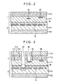
- a first semiconductor wafer 1 having a pixel array as shown in FIG. 1A and a second semiconductor wafer 2 having a logic circuit as shown in FIG. 1B are created.
- the first semiconductor wafer 1 is also referred to as a CIS substrate 1
- the second semiconductor wafer 2 is also referred to as a logic substrate 2.
- the CIS substrate 1 is configured to include a silicon substrate F12 and an inter-layer film F11 on the silicon substrate F12.
- the inter-layer film F11 also includes a photodiode PD, a line CC, a pixel transistor and a transfer transistor.
- the photodiode PD is a photoelectric conversion element.
- the pixel transistor and the transfer transistor are not shown in the figure.
- Each of the pixel transistor and the transfer transistor includes a source area, a drain area and multilayer lines surrounding the areas.
- the logic substrate 2 is configured to include a silicon substrate F22 and an inter-layer film F21 on the silicon substrate F22.
- the logic substrate 2 also includes a plurality of MOS transistors not shown in the figure. Each of the MOS transistors has an element separation area, a source area and a drain area.
- the logic substrate 2 also includes a logic circuit for processing signals and multilayer lines CL.
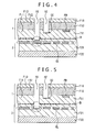
- the diameter of each of the holes H1 and H2 is set at a value in a range of typically 1 to 5 microns.
- the depth of each of the holes H1 and H2 is set at a value in a range of typically 3 to 15 microns.
- the width of the line CL directly beneath the bottom of the hole H1 is set at a value not smaller than 1 micron.
- the width of the line CC directly beneath the bottom of the hole H2 is set at a value not smaller than 1 micron.
- the thickness of each of the lines CL and CC is set at a value in a range of 100 nanometers to 1 micron.
- the oxidized film of the bottom of the hole H1 is removed by etching.
- the oxidized film of the bottom of the hole H2 is removed by etching.
- variations of the oxidized film at the bottom of the hole H1 increase with ease. For this reason, as indicated by a member enclosed by a dotted line as shown in FIG. 3 , it is ideally desirable that the hole H1 has such a depth that the bottom of the hole H1 reaches the line CL. In actuality, however, the bottom of the hole H1 is shifted from the line CL.
- the hole H1 has such a depth that the bottom of the hole H1 does not reach the line CL.
- the state in which the bottom of the hole H1 does not reach the line CL is a state of the so-called under-etching. In this case, it is feared that the connection is bad or, to be more specific, the connection is open.
- the boundary surface between the aluminum layer and the through-silicon via TSV1 is oxidized during the process of creating the through-silicon via TSV1, so that the contact resistance increases.
- the reliability of the line deteriorates. It is to be noted that, in this case, the reliability of the line indicates the degree of EM (Electronic Migration) tolerability for the line and the degree of SM (Stress Migration) tolerability for the line.
- the control of the depth of the through-silicon via TSV1 is difficult because it is necessary to take depth variations of the through-silicon via TSV1 into consideration.
- the resistance of contact between the through-silicon via TSV1 made of copper and the line made of aluminum increases because a nitride-titan (TiN) layer is included at a location between the through-silicon via TSV1 and the line.
- TiN nitride-titan
- the through-silicon via made of copper and the line made of aluminum serve respectively as a through-silicon via and a line which form the semiconductor device, it is ideal that the depth of the hole for the through-silicon via is relatively easy to control, the resistance of the connection member is low and the reliability of the line is high.
- the contact area is an area in which the through-silicon via made of copper is brought into contact with the line made of aluminum.
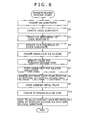
- the flowchart begins with a step S1 at which the first semiconductor wafer 1 having an array of pixels is created as shown in FIG. 1A .
- the first semiconductor wafer 1 is also referred to as the CIS substrate 1.
- the side of the CIS substrate 1 is ground to form a thin film as a whole.
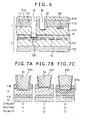
- each of the holes H1 and H2 shown in FIG. 9 an insulation film is formed to serve as an insulator against the CIS substrate 1.
- the diameter of each of the holes H1 and H2 is set at a value in a range of typically 1 to 5 microns.
- the depth of each of the holes H1 and H2 is set at a value in a range of typically 3 to 15 microns.
- the width of the line CL directly beneath the bottom of the hole H1 is set at a value not smaller than 1 micron.
- the width of the line CC directly beneath the bottom of the hole H2 is set at a value not smaller than 1 micron.
- the thickness of each of the lines CL and CC is set at a value in a range of 100 nanometers to 1 micron.
- the oxidized film of the bottom of the hole H1 is removed by carrying out an etching process.
- the oxidized film of the bottom of the hole H2 is removed by carrying out an etching process.
- a barrier metal layer exists in each of the line CC directly beneath the hole H2 and the line CL directly beneath the hole H1, a condition of a high-select ratio is a condition desirable for this step.
- the barrier metal layer is a layer made of titan nitride (TiN), titan (Ti), tantalum (Ta) or tantalum nitride (TaN) or a stack of layers made of such materials, the etching process is carried under conditions described as follows.
- the etching process results in a high-resistance layer OF created on the upper surface of the line CL.
- the high-resistance layer OF are a nitride film layer and an oxide film layer.
- a natural oxide film serving as the high-resistance layer OF is created.
- a barrier metal film BM is created on each of the surfaces of the holes H1 and H2 by adoption of the sputtering method.
- the high-resistance layer OF created on the upper surface of the line CL is removed.
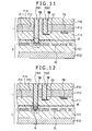
- the whole of the CIS substrate 1 and the logic substrate 2 is heated by carrying out a thermal treatment in order to diffuse aluminum (Al) and copper (Cu) into each other at a location between the through-silicon via TSV1 and the line CL so that a contact area G between the through-silicon via TSV1 and the line CL is alloyed as shown in FIG. 12 .
- the heating temperature is set at about 400°C whereas the heating environment can be a vacuum environment, the atmosphere, an oxygen environment or a nitrogen environment. The thermal treatment is carried out for about one hour.
- the contact area G between the through-silicon via TSV1 made of copper Cu and the line CL made of aluminum Al is alloyed.
- the depth of the through-silicon via TSV1 is relatively easy to control because the line CL does not retrogress and is not oxidized due to the fact that the contact area G is alloyed.
- the contact area G is alloyed, the resistance decreases and the reliability of the line CL can be improved.
- the through-silicon via TSV1 made of copper Cu has a large size of about several microns so that the volume occupied by the copper Cu is extremely large. Thus, almost no voids are generated.
- the alloyed section itself has excellent reliability, stress is structurally concentrated so that it is possible to improve the presumably weak EM and SM tolerability properties of the connection member between the edge of the through-silicon via and the surface of the line. Thus, the wiring reliability can be improved.
- the above description has explained a typical configuration of a semiconductor device used as a solid-state imaging device of the rear-surface radiation type.
- the scope of the present technology is by no means limited to the solid-state imaging device. That is to say, the present technology can also be applied to other semiconductor devices.
- the above description has explained a typical case in which copper Cu is used as a material for making the through-silicon vias, aluminum Al is used as a material for making the lines and the contact area is alloyed into a CuAl alloy.
- the through-silicon vias and the lines may be made of any other materials as long as the other materials are materials which can be alloyed with each other.
- implementations of the present technology are by no means limited to the embodiment described above. That is to say, the embodiment can be changes in a variety of ways in a range not deviating from essentials of the present technology.
- each of the steps of the flowchart described earlier can be carried out as an operation or divided into a plurality of operations.
Landscapes
- Internal Circuitry In Semiconductor Integrated Circuit Devices (AREA)
- Solid State Image Pick-Up Elements (AREA)
Applications Claiming Priority (1)
| Application Number | Priority Date | Filing Date | Title |
|---|---|---|---|
| JP2011216930A JP2013077711A (ja) | 2011-09-30 | 2011-09-30 | 半導体装置および半導体装置の製造方法 |
Publications (2)
| Publication Number | Publication Date |
|---|---|
| EP2575174A2 true EP2575174A2 (de) | 2013-04-03 |
| EP2575174A3 EP2575174A3 (de) | 2013-08-21 |
Family
ID=47040538
Family Applications (1)
| Application Number | Title | Priority Date | Filing Date |
|---|---|---|---|
| EP12184812.1A Withdrawn EP2575174A3 (de) | 2011-09-30 | 2012-09-18 | Halbleiterbauelement und Verfahren zur Herstellung eines Halbleiterbauelements |
Country Status (4)
| Country | Link |
|---|---|
| US (4) | US9287311B2 (de) |
| EP (1) | EP2575174A3 (de) |
| JP (1) | JP2013077711A (de) |
| CN (2) | CN108110023B (de) |
Cited By (1)
| Publication number | Priority date | Publication date | Assignee | Title |
|---|---|---|---|---|
| CN104332464A (zh) * | 2014-08-28 | 2015-02-04 | 武汉新芯集成电路制造有限公司 | 一种功率器件与控制器件的集成工艺 |
Families Citing this family (25)
| Publication number | Priority date | Publication date | Assignee | Title |
|---|---|---|---|---|
| US8736069B2 (en) * | 2012-08-23 | 2014-05-27 | Macronix International Co., Ltd. | Multi-level vertical plug formation with stop layers of increasing thicknesses |
| JP6041607B2 (ja) | 2012-09-28 | 2016-12-14 | キヤノン株式会社 | 半導体装置の製造方法 |
| JP6128787B2 (ja) * | 2012-09-28 | 2017-05-17 | キヤノン株式会社 | 半導体装置 |
| US8987914B2 (en) | 2013-02-07 | 2015-03-24 | Macronix International Co., Ltd. | Conductor structure and method |
| US20140252561A1 (en) * | 2013-03-08 | 2014-09-11 | Qualcomm Incorporated | Via-enabled package-on-package |
| US8993429B2 (en) | 2013-03-12 | 2015-03-31 | Macronix International Co., Ltd. | Interlayer conductor structure and method |
| US9214351B2 (en) | 2013-03-12 | 2015-12-15 | Macronix International Co., Ltd. | Memory architecture of thin film 3D array |
| US9117526B2 (en) | 2013-07-08 | 2015-08-25 | Macronix International Co., Ltd. | Substrate connection of three dimensional NAND for improving erase performance |
| US8970040B1 (en) | 2013-09-26 | 2015-03-03 | Macronix International Co., Ltd. | Contact structure and forming method |
| US9070447B2 (en) | 2013-09-26 | 2015-06-30 | Macronix International Co., Ltd. | Contact structure and forming method |
| US9343322B2 (en) | 2014-01-17 | 2016-05-17 | Macronix International Co., Ltd. | Three dimensional stacking memory film structure |
| US9304283B2 (en) * | 2014-05-22 | 2016-04-05 | Texas Instruments Incorporated | Bond-pad integration scheme for improved moisture barrier and electrical contact |
| US9721964B2 (en) | 2014-06-05 | 2017-08-01 | Macronix International Co., Ltd. | Low dielectric constant insulating material in 3D memory |
| US9356040B2 (en) | 2014-06-27 | 2016-05-31 | Macronix International Co., Ltd. | Junction formation for vertical gate 3D NAND memory |
| JP6404787B2 (ja) * | 2014-09-26 | 2018-10-17 | 信越化学工業株式会社 | ウエハ加工体、ウエハ加工用仮接着材、及び薄型ウエハの製造方法 |
| US9379129B1 (en) | 2015-04-13 | 2016-06-28 | Macronix International Co., Ltd. | Assist gate structures for three-dimensional (3D) vertical gate array memory structure |
| US9478259B1 (en) | 2015-05-05 | 2016-10-25 | Macronix International Co., Ltd. | 3D voltage switching transistors for 3D vertical gate memory array |
| KR102290020B1 (ko) * | 2015-06-05 | 2021-08-19 | 삼성전자주식회사 | 스택드 칩 구조에서 소프트 데이터 페일 분석 및 구제 기능을 제공하는 반도체 메모리 장치 |
| US9425209B1 (en) | 2015-09-04 | 2016-08-23 | Macronix International Co., Ltd. | Multilayer 3-D structure with mirror image landing regions |
| CN106505030B (zh) * | 2015-09-06 | 2019-07-26 | 中芯国际集成电路制造(上海)有限公司 | 硅通孔结构的制备方法 |
| US10854657B2 (en) * | 2016-01-18 | 2020-12-01 | Sony Corporation | Solid-state image pickup element and electronic apparatus |
| CN108701614A (zh) * | 2016-02-29 | 2018-10-23 | Towerjazz松下半导体有限公司 | 半导体装置及其制造方法 |
| US10296698B2 (en) * | 2016-12-14 | 2019-05-21 | Globalfoundries Inc. | Forming multi-sized through-silicon-via (TSV) structures |
| JP2021535613A (ja) * | 2018-09-04 | 2021-12-16 | 中芯集成電路(寧波)有限公司 | ウェハレベルパッケージ方法及びパッケージ構造 |
| US11488840B2 (en) * | 2021-01-11 | 2022-11-01 | Nanya Technology Corporation | Wafer-to-wafer interconnection structure and method of manufacturing the same |
Citations (1)
| Publication number | Priority date | Publication date | Assignee | Title |
|---|---|---|---|---|
| JP2010245506A (ja) | 2009-03-19 | 2010-10-28 | Sony Corp | 半導体装置とその製造方法、及び電子機器 |
Family Cites Families (26)
| Publication number | Priority date | Publication date | Assignee | Title |
|---|---|---|---|---|
| JP2947818B2 (ja) * | 1988-07-27 | 1999-09-13 | 株式会社日立製作所 | 微細孔への金属穴埋め方法 |
| US5262354A (en) | 1992-02-26 | 1993-11-16 | International Business Machines Corporation | Refractory metal capped low resistivity metal conductor lines and vias |
| JPH06244186A (ja) * | 1993-02-16 | 1994-09-02 | Kawasaki Steel Corp | 多層配線構造の半導体装置及びその製造方法 |
| US6285082B1 (en) | 1995-01-03 | 2001-09-04 | International Business Machines Corporation | Soft metal conductor |
| US6565729B2 (en) * | 1998-03-20 | 2003-05-20 | Semitool, Inc. | Method for electrochemically depositing metal on a semiconductor workpiece |
| JP4083921B2 (ja) * | 1998-05-29 | 2008-04-30 | 株式会社東芝 | 半導体装置の製造方法 |
| JP2000021892A (ja) * | 1998-06-26 | 2000-01-21 | Nec Corp | 半導体装置の製造方法 |
| JP2000353703A (ja) * | 1999-06-11 | 2000-12-19 | Sony Corp | 半導体装置の製造方法 |
| JP3329380B2 (ja) * | 1999-09-21 | 2002-09-30 | 日本電気株式会社 | 半導体装置およびその製造方法 |
| US6727593B2 (en) * | 2001-03-01 | 2004-04-27 | Kabushiki Kaisha Toshiba | Semiconductor device with improved bonding |
| JP4123415B2 (ja) * | 2002-05-20 | 2008-07-23 | ソニー株式会社 | 固体撮像装置 |
| JP2004273523A (ja) * | 2003-03-05 | 2004-09-30 | Renesas Technology Corp | 配線接続構造 |
| US20060246699A1 (en) * | 2005-03-18 | 2006-11-02 | Weidman Timothy W | Process for electroless copper deposition on a ruthenium seed |
| US20060244138A1 (en) * | 2005-04-27 | 2006-11-02 | International Business Machines Corporation | Techniques for improving bond pad performance |
| JP4280277B2 (ja) * | 2006-09-28 | 2009-06-17 | 株式会社神戸製鋼所 | 表示デバイスの製法 |
| FR2910707B1 (fr) * | 2006-12-20 | 2009-06-12 | E2V Semiconductors Soc Par Act | Capteur d'image a haute densite d'integration |
| US7791198B2 (en) * | 2007-02-20 | 2010-09-07 | Nec Electronics Corporation | Semiconductor device including a coupling region which includes layers of aluminum and copper alloys |
| JP4600576B2 (ja) * | 2008-05-08 | 2010-12-15 | 株式会社デンソー | 半導体装置およびその製造方法 |
| JP2009295676A (ja) * | 2008-06-03 | 2009-12-17 | Oki Semiconductor Co Ltd | 半導体装置及びその製造方法 |
| JP2010080897A (ja) * | 2008-09-29 | 2010-04-08 | Panasonic Corp | 半導体装置及びその製造方法 |
| JP5493165B2 (ja) * | 2009-09-29 | 2014-05-14 | 富士通セミコンダクター株式会社 | 半導体装置の製造方法 |
| JP5442394B2 (ja) * | 2009-10-29 | 2014-03-12 | ソニー株式会社 | 固体撮像装置とその製造方法、及び電子機器 |
| JP5489705B2 (ja) * | 2009-12-26 | 2014-05-14 | キヤノン株式会社 | 固体撮像装置および撮像システム |
| JP5853351B2 (ja) | 2010-03-25 | 2016-02-09 | ソニー株式会社 | 半導体装置、半導体装置の製造方法、及び電子機器 |
| US20120001336A1 (en) * | 2010-07-02 | 2012-01-05 | Texas Instruments Incorporated | Corrosion-resistant copper-to-aluminum bonds |
| JP5640630B2 (ja) | 2010-10-12 | 2014-12-17 | ソニー株式会社 | 固体撮像装置、固体撮像装置の製造方法、及び電子機器 |
-
2011
- 2011-09-30 JP JP2011216930A patent/JP2013077711A/ja active Pending
-
2012
- 2012-08-16 US US13/587,317 patent/US9287311B2/en active Active
- 2012-09-18 EP EP12184812.1A patent/EP2575174A3/de not_active Withdrawn
- 2012-09-21 CN CN201810048763.1A patent/CN108110023B/zh active Active
- 2012-09-21 CN CN201210355337.5A patent/CN103035660B/zh active Active
-
2016
- 2016-03-01 US US15/057,375 patent/US9865639B2/en not_active Expired - Fee Related
-
2018
- 2018-01-04 US US15/862,366 patent/US10586823B2/en active Active
-
2020
- 2020-01-23 US US16/750,810 patent/US11139331B2/en active Active
Patent Citations (1)
| Publication number | Priority date | Publication date | Assignee | Title |
|---|---|---|---|---|
| JP2010245506A (ja) | 2009-03-19 | 2010-10-28 | Sony Corp | 半導体装置とその製造方法、及び電子機器 |
Cited By (2)
| Publication number | Priority date | Publication date | Assignee | Title |
|---|---|---|---|---|
| CN104332464A (zh) * | 2014-08-28 | 2015-02-04 | 武汉新芯集成电路制造有限公司 | 一种功率器件与控制器件的集成工艺 |
| CN104332464B (zh) * | 2014-08-28 | 2017-06-06 | 武汉新芯集成电路制造有限公司 | 一种功率器件与控制器件的集成工艺 |
Also Published As
| Publication number | Publication date |
|---|---|
| CN103035660B (zh) | 2018-04-17 |
| US20180130842A1 (en) | 2018-05-10 |
| EP2575174A3 (de) | 2013-08-21 |
| CN103035660A (zh) | 2013-04-10 |
| US10586823B2 (en) | 2020-03-10 |
| US20160181303A1 (en) | 2016-06-23 |
| JP2013077711A (ja) | 2013-04-25 |
| US9287311B2 (en) | 2016-03-15 |
| US20200161362A1 (en) | 2020-05-21 |
| US9865639B2 (en) | 2018-01-09 |
| US11139331B2 (en) | 2021-10-05 |
| CN108110023A (zh) | 2018-06-01 |
| CN108110023B (zh) | 2019-08-09 |
| US20130082341A1 (en) | 2013-04-04 |
Similar Documents
| Publication | Publication Date | Title |
|---|---|---|
| US11139331B2 (en) | Semiconductor device and semiconductor-device manufacturing method | |
| US10818720B2 (en) | Stacked image sensor having a barrier layer | |
| KR101770077B1 (ko) | 반도체 장치와 그 제조 방법, 및 전자 기기 | |
| US8313977B2 (en) | Image sensor and method for manufacturing the same | |
| TWI441302B (zh) | 半導體裝置 | |
| TWI798198B (zh) | 半導體裝置及半導體裝置之製造方法 | |
| US20210272933A1 (en) | Semiconductor device, manufacturing method for semiconductor device, and electronic device | |
| TWI531053B (zh) | 半導體裝置與其形成方法與影像感測裝置 | |
| JP2011009645A (ja) | 半導体装置及びその製造方法 | |
| JP4987928B2 (ja) | 半導体装置の製造方法 | |
| JP2014072295A (ja) | 半導体装置の製造方法 | |
| KR102724590B1 (ko) | 금속 그리드의 제조 방법, 후면 조사형 이미지 센서 및 그 제조 방법 | |
| JP2020145284A (ja) | 半導体装置および機器 | |
| TWI604590B (zh) | 半導體裝置及其製造方法 | |
| US8105917B2 (en) | Connection pad structure for an image sensor on a thinned substrate | |
| KR20100052619A (ko) | 이미지 센서의 제조 방법 | |
| KR20100073786A (ko) | 이미지센서 및 그 제조방법 | |
| JP2013084841A (ja) | 半導体装置の製造方法、及び、半導体装置 |
Legal Events
| Date | Code | Title | Description |
|---|---|---|---|
| PUAI | Public reference made under article 153(3) epc to a published international application that has entered the european phase |
Free format text: ORIGINAL CODE: 0009012 |
|
| 17P | Request for examination filed |
Effective date: 20120918 |
|
| AK | Designated contracting states |
Kind code of ref document: A2 Designated state(s): AL AT BE BG CH CY CZ DE DK EE ES FI FR GB GR HR HU IE IS IT LI LT LU LV MC MK MT NL NO PL PT RO RS SE SI SK SM TR |
|
| AX | Request for extension of the european patent |
Extension state: BA ME |
|
| PUAL | Search report despatched |
Free format text: ORIGINAL CODE: 0009013 |
|
| AK | Designated contracting states |
Kind code of ref document: A3 Designated state(s): AL AT BE BG CH CY CZ DE DK EE ES FI FR GB GR HR HU IE IS IT LI LT LU LV MC MK MT NL NO PL PT RO RS SE SI SK SM TR |
|
| AX | Request for extension of the european patent |
Extension state: BA ME |
|
| RIC1 | Information provided on ipc code assigned before grant |
Ipc: H01L 27/146 20060101AFI20130716BHEP |
|
| STAA | Information on the status of an ep patent application or granted ep patent |
Free format text: STATUS: THE APPLICATION IS DEEMED TO BE WITHDRAWN |
|
| 18D | Application deemed to be withdrawn |
Effective date: 20140222 |