EP2573006A1 - Anordnung mit mindestens einem zu verpackenden Gegenstand und einer Transportverpackung und Herstellungsverfahren hierzu - Google Patents
Anordnung mit mindestens einem zu verpackenden Gegenstand und einer Transportverpackung und Herstellungsverfahren hierzu Download PDFInfo
- Publication number
- EP2573006A1 EP2573006A1 EP12182945A EP12182945A EP2573006A1 EP 2573006 A1 EP2573006 A1 EP 2573006A1 EP 12182945 A EP12182945 A EP 12182945A EP 12182945 A EP12182945 A EP 12182945A EP 2573006 A1 EP2573006 A1 EP 2573006A1
- Authority
- EP
- European Patent Office
- Prior art keywords
- layer
- cover
- intermediate layer
- arrangement
- plastic
- Prior art date
- Legal status (The legal status is an assumption and is not a legal conclusion. Google has not performed a legal analysis and makes no representation as to the accuracy of the status listed.)
- Granted
Links
Images


Classifications
-
- B—PERFORMING OPERATIONS; TRANSPORTING
- B65—CONVEYING; PACKING; STORING; HANDLING THIN OR FILAMENTARY MATERIAL
- B65D—CONTAINERS FOR STORAGE OR TRANSPORT OF ARTICLES OR MATERIALS, e.g. BAGS, BARRELS, BOTTLES, BOXES, CANS, CARTONS, CRATES, DRUMS, JARS, TANKS, HOPPERS, FORWARDING CONTAINERS; ACCESSORIES, CLOSURES, OR FITTINGS THEREFOR; PACKAGING ELEMENTS; PACKAGES
- B65D75/00—Packages comprising articles or materials partially or wholly enclosed in strips, sheets, blanks, tubes or webs of flexible sheet material, e.g. in folded wrappers
- B65D75/28—Articles or materials wholly enclosed in composite wrappers, i.e. wrappers formed by associating or interconnecting two or more sheets or blanks
- B65D75/30—Articles or materials enclosed between two opposed sheets or blanks having their margins united, e.g. by pressure-sensitive adhesive, crimping, heat-sealing, or welding
- B65D75/32—Articles or materials enclosed between two opposed sheets or blanks having their margins united, e.g. by pressure-sensitive adhesive, crimping, heat-sealing, or welding one or both sheets or blanks being recessed to accommodate contents
- B65D75/325—Articles or materials enclosed between two opposed sheets or blanks having their margins united, e.g. by pressure-sensitive adhesive, crimping, heat-sealing, or welding one or both sheets or blanks being recessed to accommodate contents one sheet being recessed, and the other being a flat not- rigid sheet, e.g. puncturable or peelable foil
- B65D75/327—Articles or materials enclosed between two opposed sheets or blanks having their margins united, e.g. by pressure-sensitive adhesive, crimping, heat-sealing, or welding one or both sheets or blanks being recessed to accommodate contents one sheet being recessed, and the other being a flat not- rigid sheet, e.g. puncturable or peelable foil and forming several compartments
-
- B—PERFORMING OPERATIONS; TRANSPORTING
- B65—CONVEYING; PACKING; STORING; HANDLING THIN OR FILAMENTARY MATERIAL
- B65D—CONTAINERS FOR STORAGE OR TRANSPORT OF ARTICLES OR MATERIALS, e.g. BAGS, BARRELS, BOTTLES, BOXES, CANS, CARTONS, CRATES, DRUMS, JARS, TANKS, HOPPERS, FORWARDING CONTAINERS; ACCESSORIES, CLOSURES, OR FITTINGS THEREFOR; PACKAGING ELEMENTS; PACKAGES
- B65D75/00—Packages comprising articles or materials partially or wholly enclosed in strips, sheets, blanks, tubes or webs of flexible sheet material, e.g. in folded wrappers
- B65D75/28—Articles or materials wholly enclosed in composite wrappers, i.e. wrappers formed by associating or interconnecting two or more sheets or blanks
- B65D75/30—Articles or materials enclosed between two opposed sheets or blanks having their margins united, e.g. by pressure-sensitive adhesive, crimping, heat-sealing, or welding
- B65D75/32—Articles or materials enclosed between two opposed sheets or blanks having their margins united, e.g. by pressure-sensitive adhesive, crimping, heat-sealing, or welding one or both sheets or blanks being recessed to accommodate contents
- B65D75/36—Articles or materials enclosed between two opposed sheets or blanks having their margins united, e.g. by pressure-sensitive adhesive, crimping, heat-sealing, or welding one or both sheets or blanks being recessed to accommodate contents one sheet or blank being recessed and the other formed of relatively stiff flat sheet material, e.g. blister packages, the recess or recesses being preformed
- B65D75/367—Articles or materials enclosed between two opposed sheets or blanks having their margins united, e.g. by pressure-sensitive adhesive, crimping, heat-sealing, or welding one or both sheets or blanks being recessed to accommodate contents one sheet or blank being recessed and the other formed of relatively stiff flat sheet material, e.g. blister packages, the recess or recesses being preformed and forming several compartments
-
- B—PERFORMING OPERATIONS; TRANSPORTING
- B65—CONVEYING; PACKING; STORING; HANDLING THIN OR FILAMENTARY MATERIAL
- B65D—CONTAINERS FOR STORAGE OR TRANSPORT OF ARTICLES OR MATERIALS, e.g. BAGS, BARRELS, BOTTLES, BOXES, CANS, CARTONS, CRATES, DRUMS, JARS, TANKS, HOPPERS, FORWARDING CONTAINERS; ACCESSORIES, CLOSURES, OR FITTINGS THEREFOR; PACKAGING ELEMENTS; PACKAGES
- B65D2575/00—Packages comprising articles or materials partially or wholly enclosed in strips, sheets, blanks, tubes or webs of flexible sheet material, e.g. in folded wrappers
- B65D2575/28—Articles or materials wholly enclosed in composite wrappers, i.e. wrappers formed by association or interconnecting two or more sheets or blanks
- B65D2575/30—Articles or materials enclosed between two opposed sheets or blanks having their margins united, e.g. by pressure-sensitive adhesive, crimping, heat-sealing, or welding
- B65D2575/32—Articles or materials enclosed between two opposed sheets or blanks having their margins united, e.g. by pressure-sensitive adhesive, crimping, heat-sealing, or welding one or both sheets or blanks being recessed to accommodate contents
- B65D2575/3209—Details
- B65D2575/3218—Details with special means for gaining access to the contents
- B65D2575/3245—Details with special means for gaining access to the contents by peeling off the non-rigid sheet
Definitions
- the invention describes an arrangement for the usually off-field transport of at least one object to be packaged as well as a manufacturing method for such an arrangement.
- articles to be packaged are in particular electrotechnical products and, in particular, power semiconductor modules.
- the invention will be described by means of such power semiconductor modules without limiting the generality.
- a plurality of power semiconductor modules are preferably arranged in a one- or two-dimensional matrix in a transport packaging.
- Simple cardboard boxes for example, according to DE 39 09 898 A1
- a further disadvantage is that such packaging must be opened by way of example for tests under a customs procedure and thus the power semiconductor modules can be touched directly, which may possibly lead to damage due to electrostatic discharge or due to contact with sensitive surfaces, for example silver-coated connection elements.
- the so-called Skin- packaging as exemplified by the DE 199 28 368 A1 are known, form a basic starting point of this invention and are a combination of a carton with the plastic film enclosing the goods to be packaged.
- Such packages are known to have the significant disadvantage that they are not accessible to a simple operation of opening and removing the packaged Guts.
- a package for power semiconductor modules which has a cover layer, an intermediate layer, both preferably made of paper or cardboard, and a cover sheet.
- the cover layer is formed flat with a first to be arranged power semiconductor module facing the main surface.
- the intermediate layer is arranged with its second major surface.
- the associated power semiconductor module is arranged, wherein the bottom element comes to lie on the first main surface of the cover layer, and wherein the cover sheet substantially overlaps essential parts of the housing of the at least one power semiconductor module and wherein furthermore the cover film with the first main surface of the intermediate layer is connected.
- the disadvantage here is that when opening such a package, the intermediate and / or the top layer is mechanically damaged, since parts thereof adhere to the cover sheet. Due to these damages, particles of the intermediate and / or top layer may be present as contamination of the power semiconductor modules or of the working environment.
- the invention has for its object to improve such an arrangement with at least one object to be packaged and a transport packaging, in particular, the conditions for the removal can be met in environments with increased cleanliness requirements.
- the inventive idea is based on the above-mentioned packaging of at least one article to be packaged, in particular a power semiconductor module.
- a power semiconductor module ie in particular the power semiconductor module to be packaged, preferably has a base element, for example a metallic base plate, a housing made of an insulating material and connection elements for external contacting of the power semiconductor components internally insulated from the base plate.
- the term power semiconductor module is to be understood in a broad sense and by way of example disc cells should be understood.
- the transport packaging of the arrangement according to the invention in turn has a cover layer, an intermediate layer with a recess associated with the article to be packaged, with a plurality of objects in each case an associated recess, and a cover film.
- the cover layer which is preferably designed as a composite cardboard which dissipates in its entirety, has a planar design and thus forms the basis of the transport packaging.
- On a first main surface of this cover layer a plastic layer and then the article is arranged.
- the composite of cover layer and plastic layer in turn has a plurality of openings.
- the intermediate layer is arranged, with a recess for the associated object. It is particularly preferred if the edge of the recess of the intermediate layer only to a maximum of 50%, preferably only to a maximum of 25%, directly applied to the associated object and the remaining part of the edge has a distance from the object and thereby at least one uncovered there Each additional surface forms as a partial surface of the plastic layer.
- the plastic layer and the intermediate layer without a cohesive connection between them are loose on each other.
- the cover film covers essential parts of the object to be packaged and in this case lies largely against the housing and the parts which do not lie on the plastic layer of the cover layer, for example the connection elements of the power semiconductor module.
- housing is to be understood in general terms and generally refers to the outer boundary of the object to be packaged.
- the cover film is adhesively bonded to the first main surface of the intermediate layer and in the region of the at least one additional surface with the plastic layer, wherein it is preferred if the surface of the cover film itself is formed adhesive.
- a first of the cover sheet facing main surface of the intermediate layer and the plastic layer at least in Area of the additional surface, but possibly also over the entire surface, have an adhesive layer for adhesive connection with the cover sheet.
- connection to the plastic layer has a substantially lower adhesive force by at least a factor of two than that to the intermediate layers.
- the composite of cover layer and plastic layer has a much stronger adhesive force to each other than the connection of the cover sheet to the plastic layer.
- cover sheet consists of a conductive or dissipative plastic film with or without metallbedampfter outer surface. It is equally advantageous to form the cover film at least in sections, but preferably completely, transparently.
- the intermediate layer and / or cover layer consists of cardboard or cardboard.
- a further preferred embodiment results if, in a plurality of objects arranged in a one- or two-dimensional matrix, these have a distance from one another in at least one dimension parallel to the main surface of the cover layer and parallel to a surface normal of the housing which is greater than the width of the housing in FIG this dimension.
- Fig. 1 shows a three-dimensional representation of two inventive arrangements.
- Fig. 3 shows a section through an inventive arrangement.
- Fig. 1 shows three-dimensional representation of two arrangements 1, 1 'according to the invention, each with a transport packaging 2 and a plurality of power semiconductor modules 5.
- the housing 50 and a plurality of connection elements 60 are shown.
- bottom element 40, cf. Fig. 2 here a metallic base plate
- these power semiconductor modules 5 are connected in a two-dimensional matrix on a plastic layer 130.
- the power semiconductor modules 5 are arranged on the first main surface 100 of the cover layer 10 of the respective transport packaging 2 in that the bottom element 40, cf. Fig. 2 each lie directly on top of it.
- an intermediate layer 20 is arranged with its second major surface 210 without being adhesively connected thereto.
- This intermediate layer 20 has a plurality of recesses 230, which are each assigned to a power semiconductor module 5.
- the power semiconductor module 5 is arranged in this recess 230 such that the edge 220 of the recess 230 rests directly on the housing 50 of the power semiconductor module 5 only at a few sections.
- additional surfaces 140 of the plastic layer 130 remain between the housing 50 of the power semiconductor module 5 and the edge 220 of the recess 230, whereby an intermediate region 240 is formed.
- edge 220 of the recess 230 does not abut against the power semiconductor module 5. This creates an additional surface 140 circumferentially around the power semiconductor module. 5
- the transport packaging 2 shown here has a perforation 70 between the respective power semiconductor components 5 in the second arrangement 1 ', cf. also Fig. 3 in order to simplify the singulation of the packaged power semiconductor modules 5.
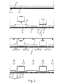
- Fig. 2 shows in four partial illustrations essential steps of the production of an inventive arrangement.
- a plastic layer 130 is arranged on the first main surface 100 of a cover layer 10 and permanently connected thereto.
- the cover layer 10 here consists of cardboard or cardboard and has a preferred thickness between 0.2 mm and 2 mm, while the plastic layer is preferably made of PET (polyethylene terephthalate) or PP (polypropylene) and has a preferred thickness in the range between 5 .mu.m and 30 .mu.m.
- this composite is provided with a plurality of apertures 150 formed from surface to surface. The diameter of these recesses is preferably between 0.1 mm and 1 mm, thereby allowing the composite to apply a negative pressure to the opposite side.
- an intermediate layer 20 with recesses 230 and in these recesses in each case a power semiconductor module 5 is arranged.
- additional surfaces 140 are freed on the plastic layer 130, which are not covered by the power semiconductor modules 5.
- Neither the intermediate layer 20, nor the respective power semiconductor module 5 are in this case adhesively connected to the plastic layer 130.
- the positioning of the power semiconductor modules 5 takes place, cf. Fig. 1 by a suitable design of the respective recess 230.
- a cover sheet 30 above the intermediate layer 20 and the power semiconductor modules 5, this overlapping arranged it may be necessary to apply the cover film at a temperature of between 80.degree. C. and 160.degree. C., in particular between 90.degree. C. and 110.degree. C., before direct placement on the power semiconductor modules and in a position which is still objectionable thereto.
- the elasticity of the cover sheet is temporarily increased and thus the subsequent positive connection with the power semiconductor module substantially improved than without temperature exposure would be done.
- the cover film 30 is sucked onto the intermediate layer 20, the additional surfaces 140 and the power semiconductor modules 5 to the second main surface 110 through the apertures 150.
- an adhesive connection between the intermediate layer and the additional surfaces 140 forms with the cover film 30. It is essential here that the adhesive holding force between the cover film 30 and the intermediate layer 20 is greater by at least a factor of 2 than the adhesive holding force between the cover film 30 and the plastic layer 130. This configuration avoids, as described above, that neither Cover layer 10 nor the intermediate layer 20 is damaged when opening the transport packaging.
- Fig. 3 shows a detail of a section along the line AA by an inventive arrangement (1) according to Fig. 1 , Shown here is the cover layer 10 of the transport packaging 2 with the plastic layer 130 arranged on its first main surface 100.
- the power semiconductor module 5 to be packaged is arranged on the plastic layer 130 at the same distance from each other in a matrix-like manner. Of the power semiconductor modules 5 to be packaged, only one bottom element 40, one housing 50 and one connection element 60 are shown.
- connection elements 60 are located on the side of the power semiconductor module 5 opposite the cover layer 10.
- the intermediate layer 20 also has recesses 230, whereby the associated power semiconductor module 5 comprises in its lower region and is fixed in its position. In this case, however, there remains an additional surface 140 of the plastic layer 130 which is not covered by the power semiconductor module 5 or the intermediate layer 20.
- the edge 220 of the recess 230 abuts a maximum of 50%, preferably only a maximum of 25%, directly on the associated power semiconductor module 5 and the remaining part of the edge 220 a distance of at least 2mm, preferably at least 5 mm to the power semiconductor module 5 and thus forms an intermediate region 240 above the additional surface 140.
- a direct concern is at least in some places, preferably in the corners of the power semiconductor module 5, cf. Fig. 1 , necessary so that the fixation of the power semiconductor module 5 is ensured in their position to each other.
- the cover film 30 is here only for the sake of clarity spaced from the cover 10 and the intermediate layer 20 and also shown spaced from the power semiconductor modules 5.
- the cover film 30 is adhesively bonded to the first main surface 200 of the intermediate layer 20, as is the plastic layer 130 in the region of the additional surfaces 140.
- the cover sheet 30 is, as far as its flexibility allows, to the power semiconductor modules 5 and encloses them each to the cover layer 10 back.
- Typical dimensions for such power semiconductor modules 5 are, without thereby deriving a limitation, a length in the range of 3 cm to 15 cm with a width 500 and height of 1 cm to 6 cm.
- the cover layer 10 of the transport packaging 2 has a typical thickness of 0.2 mm to 2 mm, the intermediate layer 20 has a thickness of 0.5 to 3 mm, while the cover film 30 has a thickness of 50 ⁇ m to 250 ⁇ m.
- the inventive arrangement 1 according to Fig. 3 is further configured such that the distance 700 of the power semiconductor modules 5 to one another is greater than the width 500 of a power semiconductor module 5, whereby it is possible to provide a second dotted arrangement 1 'offset by half the distance to the first arrangement 1 and rotated by 180 °, see. Fig. 1 , resulting in a compact overall arrangement with high packing density with simultaneous sufficient fixation of the individual power semiconductor modules 5 to each other.
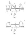
- FIG. 4 and 5 shows a further section along the line BB by an inventive arrangement 1 according to Fig. 1 wherein a particular advantage of the arrangement becomes apparent.
- Fig. 4 again shows a power semiconductor module 5 and a part of the transport packaging 2.
- the cover layer 10 is shown together with the plastic layer 130 partially separated from the intermediate layer 20.
- This representation corresponds to the opening of the transport packaging 2 in order to remove a power semiconductor module 5 from this. In this case, only the connection between the additional surface 140 of the plastic layer 130 and the cover film 30 in the intermediate region 240 is separated.
- Fig. 5 now shows a further step of removing a power semiconductor module 5 from the transport packaging 2.
- the intermediate layer 20 has been pressed in the direction of the surface normal of their first major surface 200 until the intermediate layer 20 is approximately on the plane formed by the top of the housing 50.
- the cover sheet 30 is at least partially detached from the housing 50 of the power semiconductor module 5, whereby this can be removed easily and without the use of tools from the transport packaging 2.
Landscapes
- Chemical & Material Sciences (AREA)
- Composite Materials (AREA)
- Engineering & Computer Science (AREA)
- Mechanical Engineering (AREA)
- Packaging Frangible Articles (AREA)
- Buffer Packaging (AREA)
- Cartons (AREA)
Abstract
Description
- Die Erfindung beschreibt eine Anordnung zum meist außerbetrieblichen Transport von mindestens einem zu verpackenden Gegenstand ebenso wie ein Herstellungsverfahren für eine derartige Anordnung. Zu verpackende Gegenstände im Sinne dieser Druckschrift sind insbesondere elektrotechnisches Produkte und hierbei insbesondere Leistungshalbleitermodule. Im Folgenden wird daher ohne Beschränkung der Allgemeinheit die Erfindung mittels derartiger Leistungshalbleitermodule beschrieben. Hierbei sind bevorzugt eine Mehrzahl von Leistungshalbleitermodulen in einer ein- oder zweidimensionalen Matrix in einer Transportverpackung angeordnet.
- Es ist grundsätzlich eine Vielzahl verschiedener Transportverpackungen für Leistungshalbleitermodule, wie einfache Kartonagen oder Kunststoffblister mit Grundkörper und Deckel bekannt. Aus der Verpackung von Gütern für Endverbraucher sind sog. Skin- Verpackungen bekannt. Einfache Kartonagen beispielsweise gemäß der
DE 39 09 898 A1 weisen in der Regel den Nachteil auf, dass sie die Leistungshalbleitermodule nicht ausreichend vor mechanischen Einwirkungen beim Transport schützen. Ein weiterer Nachteil ist, dass derartige Verpackung beispielhaft für Prüfungen im Rahmen eines Zollverfahren geöffnet werden müssen und somit die Leistungshalbleitermodule direkt berührt werden können, was möglicherweise zu Schäden aufgrund elektrostatischer Entladung oder aufgrund der Berührung empfindlicher Oberflächen, beispielhaft silberbeschichteter Anschlusselemente, führen kann. - Die sog. Skin- Verpackungen, wie sie beispielhaft aus der
DE 199 28 368 A1 bekannt sind, bilden einen grundlegenden Ausgangspunkt dieser Erfindung und sind eine Kombination eines Kartons mit einer das zu verpackende Gut umschließenden Kunststofffolie. Derartige Verpackungen weisen bekanntermaßen den wesentlichen Nachteil auf, dass sie einem einfachen Vorgang des Öffnens und Entnehmen des verpackten Guts nicht zugänglich sind. - Aus der
DE 10 2010 005 048 A1 ist eine Verpackung für Leistungshalbleitermodule bekannt die eine Decklage, eine Zwischenlage, beide vorzugsweise aus Papier oder Pappe, und eine Deckfolie aufweist. Hierbei ist die Decklage flächig ausgebildet mit einer ersten dem anzuordnenden Leistungshalbleitermodul zugewandten Hauptfläche. Auf dieser ersten Hauptfläche der Decklage ist die Zwischenlage mit ihrer zweiten Hauptfläche angeordnet. In der mindestens einen Ausnehmungen auf der ersten Hauptfläche der Decklage ist das zugeordnete Leistungshalbleitermodul angeordnet, wobei dessen Bodenelement auf der ersten Hauptfläche der Decklage zu liegen kommt, und wobei die Deckfolie wesentliche Teile des Gehäuses des mindestens einen Leistungshalbleitermoduls anliegend überdeckt und wobei weiterhin die Deckfolie mit der ersten Hauptfläche der Zwischenlage verbunden ist. Nachteilig hierbei ist, dass bei der Öffnung einer derartigen Verpackung die Zwischen- und / oder die Decklage mechanisch beschädigt wird, da Teile hiervon an der Deckfolie anhaften. Durch diese Beschädigungen können Partikel der Zwischen- und/oder Decklage als Verschmutzung der Leistungshalbleitermodule oder der Arbeitsumgebung vorliegen. - Der Erfindung liegt die Aufgabe zugrunde eine derartige Anordnung mit mindestens einem zu verpackenden Gegenstand und einer Transportverpackung zu verbessern, wobei speziell die Voraussetzungen für die Entnahme auch in Umgebungen mit erhöhten Sauberkeitsanforderungen erfüllt werden können.
- Die Aufgabe wird erfindungsgemäß gelöst, durch eine Anordnung mit den Merkmalen des Anspruchs 1, sowie durch ein Verfahren gemäß Anspruch 10. Bevorzugte Ausführungsformen sind in den jeweiligen abhängigen Ansprüchen beschrieben.
- Der erfinderische Gedanke geht aus von der oben genannten Verpackung von mindestens einem zu verpackenden Gegenstand, insbesondere einem Leistungshalbleitermodul. Im Folgenden wird ohne diesbezügliche Beschränkung der Allgemeinheit jeweils auf einen zu verpackenden Gegenstand Bezug genommen bzw. nur einer beschrieben, wobei hierunter auch jeweils eine Mehrzahl von gleichartigen zu verpackenden Gegenständen verstanden werden soll. Der zu verpackende Gegenstand, also insbesondere das zu verpackende Leistungshalbleitermodul weist bevorzugt ein Bodenelement, beispielhaft eine metallische Grundplatte, ein Gehäuse aus einem Isolierstoff und Anschlusselemente zur externen Kontaktierung der intern isoliert zur Bodenplatte angeordneten Leistungshalbleiterbauelemente auf. Wobei auch hier der Begriff Leistungshalbleitermodul weitläufig zu verstehen ist und beispielhaft auch Scheibenzellen verstanden werden sollen. Die Transportverpackung der erfindungsgemäßen Anordnung weist ihrerseits eine Decklage, eine Zwischenlage mit einer dem zu verpackenden Gegenstand zugeordneten Ausnehmung, bei mehreren Gegenständen jeweils einer zugeordneten Ausnehmung, und eine Deckfolie auf. Die, vorzugsweise als ein in seiner Gesamtheit ableitfähiger Verbundkarton ausgebildet, Decklage ist flächig ausgebildet und bildet somit die Basis der Transportverpackung. Auf einer ersten Hauptfläche dieser Decklage ist eine Kunststoffschicht und hierauf der Gegenstand angeordnet. Der Verbund aus Decklage und Kunststoffschicht seinerseits weist eine Vielzahl von Durchbrüchen auf.
- Ebenfalls auf dieser Kunststoffschicht der Decklage ist die Zwischenlage angeordnet, mit einer Ausnehmung für den zugeordneten Gegenstand. Hierbei ist es besonders bevorzugt, wenn der Rand der Ausnehmung der Zwischenlage nur zu maximal 50%, bevorzugt nur zu maximal 25%, direkt an dem zugeordnete Gegenstand anliegt und der verbleibende Teil des Randes einen Abstand vom Gegenstand aufweist und hierdurch dort mindestens eine nicht bedeckte Zusatzfläche jeweils als Teilfläche der Kunststoffschicht ausbildet. Vorteilhafterweise liegen die Kunststoffschicht und die Zwischenlage ohne dass eine stoffschlüssige Verbindung zwischen ihnen besteht lose aufeinander.
- Die Deckfolie überdeckt wesentliche Teile des zu verpackenden Gegenstands und liegt hierbei weitgehend an dem Gehäuse und den nicht auf der Kunststoffschicht der Decklage zu liegen kommenden Teilen, wie beispielhaft den Anschlusselementen des Leistungshalbleitermoduls, an. Wobei hier auch der Begriff Gehäuse allgemein zu verstehen ist und im Allgemeinen die äußere Begrenzung des zu verpackenden Gegenstandes bezeichnet. Weiterhin ist die Deckfolie mit der ersten Hauptfläche der Zwischenlage und im Bereich der mindestens einen Zusatzfläche mit der Kunststoffschicht adhäsiv verbunden, wobei es bevorzugt ist, wenn die Oberfläche der Deckfolie selbst adhäsiv ausgebildet ist. Alternativ hierzu kann eine erste der Deckfolie zugewandte Hauptfläche der Zwischenlage und die Kunststoffschicht zumindest im Bereich der Zusatzfläche, aber möglicherweise auch ganzflächig, eine Haftschicht zur adhäsiven Verbindung mit der Deckfolie aufweisen. Hierbei ist es bevorzugt, wenn die Verbindung zur Kunststoffschicht eine wesentlich, um mindestens den Faktor zwei, geringere Haftkraft aufweist als diejenige zur Zwischenlagen. Selbstverständlich weist auch der Verbund aus Decklage und Kunststoffschicht eine wesentlich stärkere Haftkraft zueinander auf als die Verbindung der Deckfolie zur Kunststoffschicht.
- Es ist für den Schutz der zu verpackenden Gegenstände und falls diese elektrotechnische Produkte wie Leistungshalbleitermodule sind gegen elektrostatische Entladung bevorzugt, wenn die Deckfolie aus einer leitfähigen oder ableitfähigen Kunststofffolie mit oder ohne metallbedampfter Außenfläche besteht. Ebenso vorteilhaft ist es die Deckfolie zumindest abschnittsweise, aber bevorzugt vollständig, transparent auszubilden.
- Weiterhin ist es bevorzugt, wenn die die Zwischenlage und / oder Decklage aus Pappe oder Karton besteht. Zudem ist es vorteilhaft um die Verpackung einfach öffnen, was durch Abheben der Decklage vom Rest der Transportverpackung erfolgt, zu können, wenn die Decklage dünner und damit mechanisch weniger starr ausgebildet ist als die Zwischenlage.
- Eine weitere bevorzugte Ausführung ergibt sich, wenn bei einer Mehrzahl in einer ein- oder zweidimensionalen Matrix angeordneten Gegenständen diese in mindestens einer Dimension parallel zur Hauptfläche der Decklage und parallel zu einer Flächennormalen der Gehäuse einen Abstand voneinander aufweisen der größer ist als die Breite des Gehäuses in dieser Dimension. Somit ist es möglich zwei derartige Anordnungen mit den ersten Hauptflächen der Deckflächen zueinander und um den halben Abstand zweier Gegenstände gegeneinander versetzt zu einer Gesamtanordnung hoher Packungsdichte der Gegenstände zu kombinieren.
- Die Herstellung einer derartigen Anordnung erfolgt in erfinderischer Weise mittels dieser aufeinander folgender Herstellungsschritte:
- Anordnen und Verbinden einer Kunststoffschicht mit einer ersten Hauptfläche einer vorzugsweise aus Pappe bestehenden Decklage.
- Ausbilden einer Vielzahl von Durchbrüchen von Oberfläche zu Oberfläche durch den Verbund aus Decklage und Kunststoffschicht.
- Anordnen einer Zwischenlage mit einer Ausnehmung und von einem zu verpackenden Gegenstand, insbesondere einem Leistungshalbleitermodul, in dieser Ausnehmung, wobei hierbei mindestens eine Zusatzfläche auf der Kunststoffschicht freispart werden, die nicht von dem Gegenstand überdeckt sind. Vorzugsweise bestehen die Zwischenlage und / oder Decklage aus Pappe oder Karton. Ebenso ist es vorteilhaft wenn die Decklage dünner und damit mechanisch weniger starr ausgebildet ist als die Zwischenlage.
- Anordnen einer Deckfolie, die Zwischenlage und den Gegenstand überdeckend. Vorteilhafterweise wird die Deckfolie vor dem Anlegen des Unterdrucks die thermisch beaufschlagt. Bevorzugt wird hierbei deren Elastizität erhöht, wodurch die formschlüssige Umhüllbarkeit des zu verpackende Gegenstandes verbessert wird.
Vorteilhafterweise besteht diese Deckfolie aus einer leitfähigen oder ableitfähigen Kunststofffolie mit oder ohne metallbedampfter Außenfläche.
Ebenso ist bevorzugt, wenn die der Zwischenlage zugewandte Oberfläche der Deckfolie adhäsive, also beispielhaft mit einer Klebeschicht ausgebildet ist. Alternativ könnte eine adhäsive Schicht auf den zu bedeckenden Bereichen der Decklage, insbesondere der Kunststoffschicht, und der Zwischenlage angeordnet sein. - Anlegen eines Unterdrucks an eine zweite Hauptfläche der Decklage, wodurch durch die Durchbrüche die Deckfolie an die Zwischenlage, die mindestens eine Zusatzfläche und den Gegenstand angesaugt werden und sich adhäsive Verbindungen mit der Deckfolie ausbilden.
- Durch die erfindungsgemäß Ausgestaltung der Anordnung bzw. deren entsprechender Herstellung wird es erreicht, dass beim Öffnen der Verpackung ausschließlich die Decklage mit angeordneter Kunststoffschicht von der Deckfolie getrennte werden und hierbei die Kunststoffschicht an der Decklage verbleibt. Somit wird die Decklage nicht beschädigt. Da die Decklage nicht adhäsive mit der Zwischenlage verbunden ist, wird auch deren Oberfläche beim Öffnen der Verpackung nicht beschädigt. Somit liegen nach Öffnen der Verpackung nur unbeschädigt Oberflächen vor, wodurch auch keine Verschmutzung durch Partikel auftreten kann.
- Die erfinderische Lösung wird an Hand der Ausführungsbeispiele der
Fig. 1 bis 5 weiter erläutert. -
Fig. 1 zeigt in dreidimensionaler Darstellung zwei erfindungsgemäße Anordnungen. -
Fig. 2 zeigt wesentliche Schritte der Herstellung einer erfindungsgemäßen Anordnung. -
Fig. 3 zeigt einen Schnitt durch eine erfindungsgemäße Anordnung. -
Fig. 4 und 5 zeigt einen weiteren Schnitt durch eine erfindungsgemäße Anordnung. -
Fig. 1 zeigt in dreidimensionaler Darstellung zwei erfindungsgemäße Anordnungen 1, 1' mit jeweils einer Transportverpackung 2 und einer Mehrzahl von Leistungshalbleitermodulen 5. Von diesen Leistungshalbleitermodulen 5 sind jeweils das Gehäuse 50 und eine Mehrzahl von Anschlusselementen 60 dargestellt. Mit ihrem nicht sichtbaren Bodenelement 40, vgl.Fig. 2 , hier einer metallischen Grundplatte, sind diese Leistungshalbleitermodule 5 in einer zweidimensionalen Matrix auf eine Kunststoffschicht 130 verbunden. Die Leistungshalbleitermodule 5 sind auf der ersten Hauptfläche 100 der Decklage 10 der jeweiligen Transportverpackung 2 angeordnet, indem das Bodenelement 40, vgl.Fig. 2 jeweils direkt hierauf zu liegen kommt. - Auf dieser Kunststoffschicht 130 ist eine Zwischenlage 20 mit ihrer zweiten Hauptfläche 210 angeordnet ohne adhäsive damit verbunden zu sein. Diese Zwischenlage 20 weist eine Mehrzahl von Ausnehmungen 230 auf, die jeweils einem Leistungshalbleitermodul 5 zugeordnet sind. Hierbei ist das Leistungshalbleitermodul 5 in dieser Ausnehmung 230 derart angeordnet, dass der Rand 220 der Ausnehmung 230 nur an wenigen Abschnitten direkt an dem Gehäuse 50 des Leistungshalbleitermoduls 5 anliegt. Es verbleibt somit Zusatzflächen 140 der Kunststoffschicht 130 zwischen dem Gehäuse 50 des Leistungshalbleitermoduls 5 und dem Rand 220 der Ausnehmung 230, wodurch einen Zwischenbereich 240 ausbildet wird.
- Es kann ebenso bevorzugt sein, wenn der Rand 220 der Ausnehmung 230 nicht an dem Leistungshalbleitermodul 5 anliegt. Hierbei entsteht eine Zusatzfläche 140 umlaufend um das Leistungshalbleitermodul 5.
- Nicht dargestellt ist die transparente Deckfolie 30 der Transportverpackung 30 selbst, die die Leistungshalbleitermodule 5 mit Ausnahme ihres Bodenelements 40 umschließt und die mit der zweiten Hauptfläche 210 der Zwischenlage 20 und mit der mindestens einen Zusatzfläche 140 der Kunststoffschicht 130 adhäsiv verbunden ist. Falls nur eine umlaufend um das Leistungshalbleitermodul 5 ausgebildete Zusatzfläche 140 vorgesehen ist entsteht somit eine umlaufende adhäsive Verbindung, die das Leistungshalbleitermodul 5 quasi hermetisch einschließt und von gewissen Umwelteinflüssen, wie Feuchtigkeit, schützt.
- Bei einer hier dargestellten Mehrzahl von Leistungshalbleitermodulen 5 in einer zweidimensionalen Matrixanordnung ist es weiterhin, ebenso wie auch bei einer eindimensionalen Anordnung, vorteilhaft, wenn die Transportverpackung 2 hier dargestellt bei der zweiten Anordnung 1' zwischen den jeweiligen Leistungshalbleiterbauelementen 5 eine Perforierung 70 aufweist, vgl. auch
Fig. 3 , um das Vereinzeln der verpackten Leistungshalbleitermodule 5 zu vereinfachen. -
Fig. 2 zeigt in vier Teilabbildungen wesentliche Schritte der Herstellung einer erfindungsgemäßen Anordnung. In einem ersten Schritt wird auf der ersten Hauptfläche 100 einer Decklage 10 eine Kunststoffschicht 130 angeordnet und dauerhaft mit dieser verbunden. Die Decklage 10 besteht hierbei aus Pappe oder Karton und weist eine bevorzugte Dicke zwischen 0,2mm und 2mm auf, während die Kunststoffschicht bevorzugt aus PET (Polyethylenterephthalat) oder PP (Polypropylen) besteht und eine bevorzugte Dicke im Bereich zwischen 5µm und 30µm aufweist. Im Anschluss hieran wird dieser Verbund mit einer Vielzahl von Durchbrüchen 150 versehen, die von Oberfläche zu Oberfläche ausgebildet sind. Der Durchmesser dieser Ausnehmungen liegt bevorzugt zwischen 0,1 mm und 1 mm und gestattet es dadurch durch den Verbund hindurch einen Unterdruck an die gegenüberliegende Seite anzulegen. - In einem nächsten Schritt wird eine Zwischenlage 20 mit Ausnehmungen 230 und in diesen Ausnehmungen jeweils ein Leistungshalbleitermodul 5 angeordnet. Hierbei sind Zusatzflächen 140 auf der Kunststoffschicht 130 freispart, die nicht von den Leistungshalbleitermodulen 5 überdeckt sind. Weder die Zwischenlage 20, noch das jeweilige Leistungshalbleitermodul 5 sind hierbei adhäsive mit der Kunststoffschicht 130 verbunden. Die Positionierung der Leistungshalbleitermodule 5 erfolgt, vgl.
Fig. 1 durch eine geeignete Ausbildung der jeweiligen Ausnehmung 230. - Anschließend wird eine Deckfolie 30 oberhalb der Zwischenlage 20 und der Leistungshalbleitermodule 5 diese überdeckend angeordnet. Hierbei kann es notwendig sein vor dem direkten Anordnen an den Leistungshalbleitermodulen und in noch hiervon beanstandeter Position die Deckfolie mit einer Temperatur zwischen 80 °C und 160 °C, insbesondere zwischen 90 °C und 110 °C, zu beaufschlagen. Hierdurch wird die Elastizität der Deckfolie temporär erhöht und damit der nachfolgend Formschluss mit dem Leistungshalbleitermodul wesentlich verbessert als dies ohne Temperaturbeaufschlagung erfolgen würde. Weiterhin vorteilhafter ist es zumindest diejenige Oberfläche, die der Zwischenlage 20 und den Leistungshalbleitermodulen 5 zugewandt ist, adhäsiv ausgebildet. Alternativ hierzu kann eine erste der Deckfolie (30) zugewandte Hauptfläche (200) der Zwischenlage (20) und die Kunststoffschicht (130) zumindest im Bereich der Zusatzfläche (140) eine Haftschicht zur adhäsiven Verbindung mit der Deckfolie (30) aufweisen. Diese Haftschicht wird dabei mit einem Abscheide-, beispielhaft einem Druck-, Verfahren auf dem Bereich der Zusatzflächen aufgebracht. Falls diese Haftschicht thermisch aktiviert wird kann sie ganzflächig auf der Kunststoffschicht, oder ganzflächig mit Ausnahme der von den Leistungshalbleitermodulen überdeckten Bereichen aufgebracht werden.
- Durch Anlegen eines Unterdrucks, dargestellt durch die Pfeile an der zweiten Hauptfläche 110 der Decklage 10, wird an diese zweite Hauptfläche 110 durch die Durchbrüche 150 die Deckfolie 30 an die Zwischenlage 20, die Zusatzflächen 140 und die Leistungshalbleitermodule 5 angesaugt. Hierbei bildet sich eine adhäsive Verbindung der Zwischenlage und der Zusatzflächen 140 mit der Deckfolie 30 aus. Wesentlich hierbei ist, dass die adhäsive Haltekraft zwischen der Deckfolie 30 und der Zwischenlage 20 mindestens um den Faktor 2 größer ist als die adhäsive Haltekraft zwischen der Deckfolie 30 und der Kunststoffschicht 130. Durch diese Ausgestaltung wird es, wie oben beschrieben vermieden, dass weder die Decklage 10 noch die Zwischenlage 20 beim Öffnen der Transportverpackung beschädigt wird.
-
Fig. 3 zeigt ausschnittsweise einen Schnitt entlang der Linie A-A durch eine erfindungsgemäße Anordnung (1) gemäßFig. 1 . Dargestellt ist hier die Decklage 10 der Transportverpackung 2 mit der auf ihrer ersten Hauptfläche 100 angeordneten Kunststoffschicht 130. Auf der Kunststoffschicht 130 sind matrixartig mit gleichem Abstand zueinander die zu verpackenden Leistungshalbleitermodul 5 angeordnet. Von den zu verpackenden Leistungshalbleitermodulen 5 sind nur ein Bodenelement 40, ein Gehäuse 50 und ein Anschlusselement 60 dargestellt. - Es ist vorteilhaft diese Leistungshalbleitermodule 5 mit ihrem Bodenelement 40, das üblicherweise eine metallisch Grundplatte oder auch direkt das Substrat der internen Schaltung sein kann, auf der Kunststoffschicht 130 anzuordnen. Dies ist allerdings nicht einschränkend für die Möglichkeiten, das Leistungshalbleitermodul 5 um 90°oder 180° um eine seiner Längsachsen gedreht anzuordnen. Bei der hier vorgesehenen Ausgestaltung liegen die Anschlusselemente 60 auf der der Decklage 10 gegenüberliegender Seite des Leistungshalbleitermoduls 5.
- Weiterhin dargestellt ist die Zwischenlage 20, deren zweite Hauptfläche 210 mit der ersten Hauptfläche 100 der Decklage 10 keine adhäsive Verbindung aufweist. Vorzugsweise aber nicht beschränkend besteht die die Zwischenlage 20 wie auch die Decklage 10 aus Pappe oder Karton.
- Die Zwischenlage 20 weist weiterhin Ausnehmungen 230 auf, wodurch das zugeordnete Leistungshalbleitermodul 5 in seinem unteren Bereich umfasst und in seiner Lage fixiert wird. Es verbleibt hierbei allerdings eine Zusatzfläche 140 der Kunststoffschicht 130 die nicht von dem Leistungshalbleitermodul 5 oder der Zwischenlage 20 bedeckt ist. Auf dem gesamten Umfang des Leistungshalbleitermodul 5 ist es vorgesehen, dass der Rand 220 der Ausnehmung 230 zu maximal 50%, bevorzugt nur zu maximal 25%, direkt an dem zugeordneten Leistungshalbleitermodul 5 anliegt und der verbleibende Teil des Randes 220 einen Abstand von mindestens 2mm, vorzugsweise mindestens 5mm zum Leistungshalbleitermodul 5 aufweist und somit einen Zwischenbereich 240 oberhalb der Zusatzfläche 140 ausbildet. Ein direktes Anliegen ist allerdings zumindest an einigen Stellen, vorzugsweise in den Ecken des Leistungshalbleitermoduls 5, vgl.
Fig. 1 , notwendig, damit die Fixierung der Leistungshalbleitermodul 5 in ihrer Position zueinander gewährleistet wird. - Die Deckfolie 30 ist hier ausschließlich zur besseren Übersichtlichkeit beabstandet von der Deck- 10 bzw. der Zwischenlage 20 und auch beabstandet von den Leistungshalbleitermodulen 5 dargestellt. Im Übrigen ist die Deckfolie 30 mit der ersten Hauptfläche 200 der Zwischenlage 20, wie auch der Kunststoffschicht 130 im Bereich der Zusatzflächen 140 adhäsiv verbunden. Die Deckfolie 30 liegt, soweit deren Flexibilität dies erlaubt, an den Leistungshalbleitermodulen 5 an und umschließt sie jeweils zur Decklage 10 hin.
- Typische Abmessungen für derartige Leistungshalbleitermodule 5 sind, ohne hieraus eine Beschränkung abzuleiten, eine Länge im Bereich von 3cm bis 15cm bei einer Breite 500 und Höhe von 1 cm bis 6cm. Die Decklage 10 der Transportverpackung 2 weist eine typische Dicke von 0,2mm bis 2mm auf, die Zwischenlage 20 ein Dicke von 0,5 bis 3mm, während die Deckfolie 30 eine Dicke von 50µm bis 250µm aufweist.
- Durch die Ausgestaltung der Deckfolie 30 aus einer leitfähigen oder ableitfähigen Kunststoffschicht mit oder ohne metallbedampfter Außenfläche und der Decklage 10 aus einem leitfähigen oder ableitfähigen Verbundkarton, entsteht eine Transportverpackung 2, die einen ausreichenden Schutz gegen elektrostatische Aufladung bietet. Da die Deckfolie 30 zumindest abschnittsweise, aber bevorzugt vollständig, transparent ausgebildet ist, ist es auch zu verschiedenen Kontrollzwecken nicht nötig diese Schutzverpackung zu öffnen.
- Die erfindungsgemäße Anordnung 1 gemäß
Fig. 3 ist weiterhin derart ausgestaltet, dass der Abstand 700 der Leistungshalbleitermodule 5 zueinander größer ist als die Breite 500 eines Leistungshalbleitermoduls 5, wodurch es möglich ist eine zweite punktiert dargestellte Anordnung 1' um den halben Abstand versetzt zur ersten Anordnung 1 und um 180° gedreht vorzusehen, vgl.Fig. 1 , wodurch sich eine kompakte Gesamtanordnung mit hoher Packungsdichte bei gleichzeitiger ausreichender Fixierung der einzelnen Leistungshalbleitermodule 5 zueinander ergibt. -
Fig. 4 und 5 zeigt einen weiteren Schnitt entlang der Linie B-B durch eine erfindungsgemäße Anordnung 1 gemäßFig. 1 , wobei ein besonderer Vorteil der Anordnung offensichtlich wird.Fig. 4 zeigt wiederum ein Leistungshalbleitermodul 5 sowie einen Teil der Transportverpackung 2. Hierbei ist allerdings die Decklage 10 mitsamt der Kunststoffschicht 130 teilweise von der Zwischenlage 20 getrennt dargestellt. Diese Darstellung entspricht dem Öffnen der Transportverpackung 2, um ein Leistungshalbleitermodul 5 aus dieser zu entnehmen. Hierbei wird ausschließlich die Verbindung zwischen der Zusatzfläche 140 der Kunststoffschicht 130 und der Deckfolie 30 in dem Zwischenbereich 240 getrennt. - Hierfür ist es einerseits notwendig, dass Verbindung zwischen der Deckfolie 30 und der Zwischenlage 20 eine wesentlich höhere Haftkraft aufweist als die Verbindung der Deckfolie 30 mit der Kunststoffschicht 130. Ebenso ist es von Vorteil, wenn die die Decklage 10 dünner und damit mechanisch weniger starr ausgebildet ist als die Zwischenlage 20, da somit die Zwischenlage quasi als Halterrahmen des Restes der Transportverpackung 2 bestehen bleibt.
-
Fig. 5 zeigt nun einen weiteren Schritt der Entnahme eines Leistungshalbleitermoduls 5 aus der Transportverpackung 2. Hierbei wurde die Zwischenlage 20 in Richtung der Flächennormalen ihrer ersten Hauptfläche 200 gedrückt, bis die Zwischenlage 20 annährend auf der durch die Oberseite des Gehäuses 50 gebildeten Ebene liegt. Bei dieser Verschiebung der Zwischenlage 20 löst sich die Deckfolie 30 zumindest teilweise von dem Gehäuse 50 des Leistungshalbleitermoduls 5, wodurch dieses einfach und ohne Anwendung von Werkzeug aus der Transportverpackung 2 entnommen werden kann.
Claims (15)
- Anordnung (1) mit einem zu verpackenden Gegenstand (5) und einer Transportverpackung (2), wobei der Gegenstand (5) ein Gehäuse (50) aufweist, wobei die
Transportverpackung (2) eine Decklage (10), eine Zwischenlage (20) mit einer dem Gegenstand (5) zugeordneten Ausnehmung (230) und eine Deckfolie (30) aufweist und
hierbei die Decklage (10) flächig, mit einer ersten dem Gegenstand (5) zugewandten Hauptfläche (100) ausgebildet ist, auf dieser ersten Hauptfläche (100) der Decklage (10) eine Kunststoffschicht (130) angeordnet ist und die Decklage (10) samt Kunststoffschicht (130) eine Vielzahl von Durchbrüchen (150) aufweist, auf der Kunststoffschicht die Zwischenlage (20) mit ihrer zweiten Hauptfläche (210) angeordnet ist und in der Ausnehmung (230) der Zwischenlage (20) der dieser Ausnehmung zugeordnete Gegenstand (5) auf der Kunststoffschicht (130) angeordnet ist und hierbei die Ausnehmung (230) nicht vollständig bedeckt, sondern mindestens eine Zusatzfläche (140) freispart, wobei die Deckfolie (30) wesentliche nicht auf der Kunststoffschicht (130) zu liegen kommende Teile des Gegenstandes (5) überdeckt, hierbei weitgehend an dem Gehäuse (50) anliegt und wobei die Deckfolie (30) mit der ersten Hauptfläche (200) der Zwischenlage (20) und mit der Kunststoffschicht (130) im Bereich der mindestens einen Zusatzfläche (140) adhäsiv verbunden ist. - Anordnung nach Anspruch 1, wobei
der zu verpackende Gegenstand (5) ein elektrotechnisches Produkt insbesondere ein Leistungshalbleitermodul ist. - Anordnung (1) nach Anspruch 1, wobei
die Kunststoffschicht (130) und die Zwischenlage (20) ohne eine stoffschlüssige Verbindung lose aufeinanderliegen. - Anordnung nach Anspruch 1, wobei
die der Zwischenlage zugewandte Oberfläche der Deckfolie adhäsiv ausgebildet ist oder wobei eine erste der Deckfolie (30) zugewandte Hauptfläche (200) der Zwischenlage (20) und die Kunststoffschicht (130) zumindest im Bereich der Zusatzfläche (140) eine Haftschicht zur adhäsiven Verbindung mit der Deckfolie (30) aufweisen. - Anordnung (1) nach Anspruch 1, wobei
die adhäsive Verbindung der Deckfolie (30) mit der Zwischenlage (20) eine mindestens doppelt so hohe Haftkraft aufweist im Vergleich zur Verbindung der Deckfolie (30) mit der Zwischenfolie (130). - Anordnung (1) nach Anspruch 1, wobei
die Deckfolie (30) aus einer leitfähigen oder ableitfähigen Kunststoffschicht mit oder ohne metallbedampfter Außenfläche besteht. - Anordnung (1) nach Anspruch 1, wobei
die Zwischenlage (20) und / oder Decklage (10) aus Pappe oder Karton besteht. - Anordnung (1) nach Anspruch 1, wobei
die Decklage (10) dünner und damit mechanisch weniger starr ausgebildet ist als die Zwischenlage (20). - Anordnung (1) nach Anspruch 8, wobei
die Decklage (10) ein Dicke von 0,2mm bis 2mm und die Zwischenlage (20) eine Dicke von 0,5 bis 3mm aufweisen und damit eine wesentlich geringer Dicke aufweisen im Vergleich zur Höhe eines zu verpackenden Gegenstands (5). - Verfahren zur Herstellung einer Anordnung (1) mit einem zu verpackenden Gegenstand (5), wobei der Gegenstand (5) ein Gehäuse (50) aufweist, und einer Transportverpackung (2), gekennzeichnet durch diese aufeinanderfolgenden Herstellungsschritte:• Anordnen und Verbinden einer Kunststoffschicht (130) mit einer ersten Hauptfläche (100) einer Decklage (10);• Ausbilden einer Vielzahl von Durchbrüchen (150) von Oberfläche zu Oberfläche durch den Verbund aus Decklage (10) und Kunststoffschicht (120);• Anordnen einer Zwischenlage (20) mit einer Ausnehmung (230) und eines Gegenstandes (5) in dieser Ausnehmung (230), wobei hierbei mindestens eine Zusatzfläche (140) auf der Kunststoffschicht (130) freispart werden, die nicht von dem Gegenstand (5) überdeckt ist;• Anordnen einer Deckfolie (30), die Zwischenlage (20) und den Gegenstand (5) überdeckend;• Anlegen eines Unterdrucks an eine zweite Hauptfläche (110) der Decklage (10), wodurch durch die Durchbrüche (150) die Deckfolie (30) an die Zwischenlage (20), die Zusatzflächen (140) und den Gegenstand (5) angesaugt werden und sich adhäsive Verbindungen mit der Deckfolie (30) ausbilden.
- Verfahren nach Anspruch 10, wobei
vor dem Anlegen des Unterdrucks die Deckfolie (30) thermisch beaufschlagt wird. - Verfahren nach Anspruch 10, wobei
die Deckfolie (30) aus einer leitfähigen oder ableitfähigen Kunststoffschicht mit oder ohne metallbedampfter Außenfläche besteht. - Verfahren nach Anspruch 10, wobei
die Zwischenlage (20) und / oder Decklage (10) aus Pappe oder Karton besteht. - Verfahren nach Anspruch 10, wobei
die Decklage (10) dünner und damit mechanisch weniger starr ausgebildet ist als die Zwischenlage (20). - Verfahren nach Anspruch 11, wobei
die der Zwischenlage (20) zugewandte Oberfläche (10) der Deckfolie (30) adhäsive ausgebildet ist oder wobei eine erste der Deckfolie (30) zugewandte Hauptfläche (200) der Zwischenlage (20) und die Kunststoffschicht (130) zumindest im Bereich der Zusatzfläche (140) eine Haftschicht zur adhäsiven Verbindung mit der Deckfolie (30) aufweisen.
Applications Claiming Priority (1)
| Application Number | Priority Date | Filing Date | Title |
|---|---|---|---|
| DE102011114309.6A DE102011114309B4 (de) | 2011-09-23 | 2011-09-23 | Anordnung mit mindestens einem zu verpackenden Gegenstand und einer Transportverpackung und Herstellungsverfahren hierzu |
Publications (2)
| Publication Number | Publication Date |
|---|---|
| EP2573006A1 true EP2573006A1 (de) | 2013-03-27 |
| EP2573006B1 EP2573006B1 (de) | 2014-11-12 |
Family
ID=46796445
Family Applications (1)
| Application Number | Title | Priority Date | Filing Date |
|---|---|---|---|
| EP12182945.1A Active EP2573006B1 (de) | 2011-09-23 | 2012-09-04 | Anordnung mit mindestens einem zu verpackenden Gegenstand und einer Transportverpackung und Herstellungsverfahren hierzu |
Country Status (5)
| Country | Link |
|---|---|
| EP (1) | EP2573006B1 (de) |
| CN (2) | CN203211717U (de) |
| DE (1) | DE102011114309B4 (de) |
| DK (1) | DK2573006T3 (de) |
| ES (1) | ES2530499T3 (de) |
Families Citing this family (2)
| Publication number | Priority date | Publication date | Assignee | Title |
|---|---|---|---|---|
| DE102011114309B4 (de) * | 2011-09-23 | 2019-03-07 | Kartonveredlung Knapp GmbH | Anordnung mit mindestens einem zu verpackenden Gegenstand und einer Transportverpackung und Herstellungsverfahren hierzu |
| DE102019100951A1 (de) * | 2019-01-15 | 2020-07-16 | Osram Opto Semiconductors Gmbh | Aufbewahrungsvorrichtung |
Citations (5)
| Publication number | Priority date | Publication date | Assignee | Title |
|---|---|---|---|---|
| DE3909898A1 (de) | 1989-03-25 | 1990-09-27 | Semikron Elektronik Gmbh | Verpackungsbehaelter und zuschnitte zum herstellen eines solchen behaelters |
| EP0547518A1 (de) * | 1991-12-18 | 1993-06-23 | Hans Hagner | Skinverpackung |
| DE19928368A1 (de) | 1998-06-22 | 1999-12-23 | Hawera Probst Gmbh | Verkaufsverpackung |
| DE10204675A1 (de) * | 2002-02-06 | 2003-08-14 | Lohmann Therapie Syst Lts | Luftdichte Skinverpackung mit hoher Wasserdampfundurchlässigkeit sowie Aromaschutz |
| DE102010005048A1 (de) | 2010-01-20 | 2011-07-21 | SEMIKRON Elektronik GmbH & Co. KG, 90431 | Anordnung mit mindestens einem Leistungshalbleitermodul und mit einer Transportverpackung |
Family Cites Families (5)
| Publication number | Priority date | Publication date | Assignee | Title |
|---|---|---|---|---|
| US4757895A (en) * | 1984-09-20 | 1988-07-19 | Gelzer John R | Article packaging system |
| DE8603299U1 (de) * | 1986-02-07 | 1986-07-31 | Siemens AG, 1000 Berlin und 8000 München | Gurtverpackung von SMD-Bauteilen |
| US20040124119A1 (en) * | 2002-12-30 | 2004-07-01 | Ahn Seung Bae | Carrier tape for use in the automated parts-implanting machine for carrying parts therewith |
| DE102010005047B4 (de) * | 2010-01-20 | 2014-10-23 | Semikron Elektronik Gmbh & Co. Kg | Anordnung mit mindestens einem Leistungshalbleitermodul und mit einer Transportverpackung |
| DE102011114309B4 (de) * | 2011-09-23 | 2019-03-07 | Kartonveredlung Knapp GmbH | Anordnung mit mindestens einem zu verpackenden Gegenstand und einer Transportverpackung und Herstellungsverfahren hierzu |
-
2011
- 2011-09-23 DE DE102011114309.6A patent/DE102011114309B4/de not_active Expired - Fee Related
-
2012
- 2012-09-04 EP EP12182945.1A patent/EP2573006B1/de active Active
- 2012-09-04 DK DK12182945.1T patent/DK2573006T3/en active
- 2012-09-04 ES ES12182945T patent/ES2530499T3/es active Active
- 2012-09-24 CN CN2012204917942U patent/CN203211717U/zh not_active Withdrawn - After Issue
- 2012-09-24 CN CN201210359335.3A patent/CN103010579B/zh not_active Expired - Fee Related
Patent Citations (5)
| Publication number | Priority date | Publication date | Assignee | Title |
|---|---|---|---|---|
| DE3909898A1 (de) | 1989-03-25 | 1990-09-27 | Semikron Elektronik Gmbh | Verpackungsbehaelter und zuschnitte zum herstellen eines solchen behaelters |
| EP0547518A1 (de) * | 1991-12-18 | 1993-06-23 | Hans Hagner | Skinverpackung |
| DE19928368A1 (de) | 1998-06-22 | 1999-12-23 | Hawera Probst Gmbh | Verkaufsverpackung |
| DE10204675A1 (de) * | 2002-02-06 | 2003-08-14 | Lohmann Therapie Syst Lts | Luftdichte Skinverpackung mit hoher Wasserdampfundurchlässigkeit sowie Aromaschutz |
| DE102010005048A1 (de) | 2010-01-20 | 2011-07-21 | SEMIKRON Elektronik GmbH & Co. KG, 90431 | Anordnung mit mindestens einem Leistungshalbleitermodul und mit einer Transportverpackung |
Also Published As
| Publication number | Publication date |
|---|---|
| DE102011114309B4 (de) | 2019-03-07 |
| DK2573006T3 (en) | 2015-02-16 |
| CN103010579A (zh) | 2013-04-03 |
| ES2530499T3 (es) | 2015-03-03 |
| CN203211717U (zh) | 2013-09-25 |
| DE102011114309A1 (de) | 2013-03-28 |
| CN103010579B (zh) | 2016-08-17 |
| EP2573006B1 (de) | 2014-11-12 |
Similar Documents
| Publication | Publication Date | Title |
|---|---|---|
| DE69001028T2 (de) | Sandwich-blisterpackung fuer tabletten und dergleichen. | |
| EP1964030B1 (de) | Blisterpackung mit radiofrequenz-identifikationseinrichtung sowie verfahren zu deren herstellung | |
| DE102005058101A1 (de) | Chipkarte und Verfahren zur Herstellung einer Chipkarte | |
| WO2000075043A1 (de) | Durchdrückpackung | |
| DE102011054994A1 (de) | Gebinde mit Tragegriff, Verfahren und Vorrichtung zur Herstellung solcher Gebinde | |
| EP2663513A1 (de) | (zigaretten-)packung mit verschlussetikett | |
| DE3209756A1 (de) | Chip- oder plattenfoermige halbleitervorrichtung und ihre verpackung | |
| EP2348804B1 (de) | Anordnung mit mindestens einem Leistungshalbleitermodul und mit einer Transportverpackung | |
| EP2573006B1 (de) | Anordnung mit mindestens einem zu verpackenden Gegenstand und einer Transportverpackung und Herstellungsverfahren hierzu | |
| EP2423116B1 (de) | Flügelfixierverpackung | |
| EP1353857A1 (de) | Primärverpackungseinheit für mehrere vereinzelte filmplättchen als darreichungsformen | |
| DE102009023405A1 (de) | Verfahren zur Herstellung tragbarer Datenträger | |
| EP2347970B1 (de) | Anordnung mit mindestens einem Leistungshalbleitermodul und mit einer Transportverpackung | |
| EP2208554A2 (de) | Verfahren und Vorrichtung zur Herstellung von Aufreissdeckeln | |
| EP3438019B1 (de) | Zigarettenpackung und verfahren zum herstellen derselben | |
| EP4048604B1 (de) | Verfahren zum herstellen eines multipacks mit mehreren getränkebehältern und multipack mit mehreren getränkebehältern | |
| DE102017123011A1 (de) | Packungsmantel, Verpackung und Verfahren zur Herstellung einer Verpackung | |
| EP4000875B1 (de) | Verfahren zum herstellen einer verpackung | |
| EP2212214B1 (de) | Flacher behälter | |
| EP1185954B1 (de) | Chip-träger-verbund | |
| DE10144287A1 (de) | Verfahren zur elektrostatischen Fixierung von flächenförmigen Gegenständen auf einer Unterlage | |
| DE102016010658A1 (de) | Starre rauchwarenverpackung mit klappdeckel und mit einer inneren verpackung mit an dem deckel angebrachter versiegelungslasche sowie zugehörige falttechnik | |
| EP3322647B1 (de) | Blisterverpackung und verfahren zur entnahme eines produkts aus der blisterverpackung | |
| DE20204432U1 (de) | Verpackungsflächenstück mit Abhäsivbeschichtung und Verpackungsfläche mit Abhäsivbeschichtungen | |
| DE102017123010A1 (de) | Packungsmantel, Verpackung und Verfahren zur Herstellung einer Verpackung |
Legal Events
| Date | Code | Title | Description |
|---|---|---|---|
| PUAI | Public reference made under article 153(3) epc to a published international application that has entered the european phase |
Free format text: ORIGINAL CODE: 0009012 |
|
| AK | Designated contracting states |
Kind code of ref document: A1 Designated state(s): AL AT BE BG CH CY CZ DE DK EE ES FI FR GB GR HR HU IE IS IT LI LT LU LV MC MK MT NL NO PL PT RO RS SE SI SK SM TR |
|
| AX | Request for extension of the european patent |
Extension state: BA ME |
|
| 17P | Request for examination filed |
Effective date: 20131002 |
|
| RBV | Designated contracting states (corrected) |
Designated state(s): AL AT BE BG CH CY CZ DE DK EE ES FI FR GB GR HR HU IE IS IT LI LT LU LV MC MK MT NL NO PL PT RO RS SE SI SK SM TR |
|
| RIC1 | Information provided on ipc code assigned before grant |
Ipc: B65D 75/36 20060101ALI20140523BHEP Ipc: B65D 75/32 20060101AFI20140523BHEP |
|
| GRAP | Despatch of communication of intention to grant a patent |
Free format text: ORIGINAL CODE: EPIDOSNIGR1 |
|
| INTG | Intention to grant announced |
Effective date: 20140721 |
|
| GRAS | Grant fee paid |
Free format text: ORIGINAL CODE: EPIDOSNIGR3 |
|
| GRAA | (expected) grant |
Free format text: ORIGINAL CODE: 0009210 |
|
| AK | Designated contracting states |
Kind code of ref document: B1 Designated state(s): AL AT BE BG CH CY CZ DE DK EE ES FI FR GB GR HR HU IE IS IT LI LT LU LV MC MK MT NL NO PL PT RO RS SE SI SK SM TR |
|
| REG | Reference to a national code |
Ref country code: GB Ref legal event code: FG4D Free format text: NOT ENGLISH |
|
| REG | Reference to a national code |
Ref country code: CH Ref legal event code: EP |
|
| REG | Reference to a national code |
Ref country code: AT Ref legal event code: REF Ref document number: 695571 Country of ref document: AT Kind code of ref document: T Effective date: 20141115 |
|
| REG | Reference to a national code |
Ref country code: IE Ref legal event code: FG4D Free format text: LANGUAGE OF EP DOCUMENT: GERMAN |
|
| REG | Reference to a national code |
Ref country code: DE Ref legal event code: R096 Ref document number: 502012001567 Country of ref document: DE Effective date: 20141224 |
|
| REG | Reference to a national code |
Ref country code: DK Ref legal event code: T3 Effective date: 20150212 |
|
| REG | Reference to a national code |
Ref country code: NL Ref legal event code: T3 |
|
| REG | Reference to a national code |
Ref country code: SE Ref legal event code: TRGR Ref country code: ES Ref legal event code: FG2A Ref document number: 2530499 Country of ref document: ES Kind code of ref document: T3 Effective date: 20150303 |
|
| PG25 | Lapsed in a contracting state [announced via postgrant information from national office to epo] |
Ref country code: IS Free format text: LAPSE BECAUSE OF FAILURE TO SUBMIT A TRANSLATION OF THE DESCRIPTION OR TO PAY THE FEE WITHIN THE PRESCRIBED TIME-LIMIT Effective date: 20150312 Ref country code: PT Free format text: LAPSE BECAUSE OF FAILURE TO SUBMIT A TRANSLATION OF THE DESCRIPTION OR TO PAY THE FEE WITHIN THE PRESCRIBED TIME-LIMIT Effective date: 20150312 Ref country code: FI Free format text: LAPSE BECAUSE OF FAILURE TO SUBMIT A TRANSLATION OF THE DESCRIPTION OR TO PAY THE FEE WITHIN THE PRESCRIBED TIME-LIMIT Effective date: 20141112 Ref country code: NO Free format text: LAPSE BECAUSE OF FAILURE TO SUBMIT A TRANSLATION OF THE DESCRIPTION OR TO PAY THE FEE WITHIN THE PRESCRIBED TIME-LIMIT Effective date: 20150212 Ref country code: LT Free format text: LAPSE BECAUSE OF FAILURE TO SUBMIT A TRANSLATION OF THE DESCRIPTION OR TO PAY THE FEE WITHIN THE PRESCRIBED TIME-LIMIT Effective date: 20141112 |
|
| PG25 | Lapsed in a contracting state [announced via postgrant information from national office to epo] |
Ref country code: HR Free format text: LAPSE BECAUSE OF FAILURE TO SUBMIT A TRANSLATION OF THE DESCRIPTION OR TO PAY THE FEE WITHIN THE PRESCRIBED TIME-LIMIT Effective date: 20141112 Ref country code: RS Free format text: LAPSE BECAUSE OF FAILURE TO SUBMIT A TRANSLATION OF THE DESCRIPTION OR TO PAY THE FEE WITHIN THE PRESCRIBED TIME-LIMIT Effective date: 20141112 Ref country code: LV Free format text: LAPSE BECAUSE OF FAILURE TO SUBMIT A TRANSLATION OF THE DESCRIPTION OR TO PAY THE FEE WITHIN THE PRESCRIBED TIME-LIMIT Effective date: 20141112 Ref country code: CY Free format text: LAPSE BECAUSE OF FAILURE TO SUBMIT A TRANSLATION OF THE DESCRIPTION OR TO PAY THE FEE WITHIN THE PRESCRIBED TIME-LIMIT Effective date: 20141112 Ref country code: PL Free format text: LAPSE BECAUSE OF FAILURE TO SUBMIT A TRANSLATION OF THE DESCRIPTION OR TO PAY THE FEE WITHIN THE PRESCRIBED TIME-LIMIT Effective date: 20141112 Ref country code: GR Free format text: LAPSE BECAUSE OF FAILURE TO SUBMIT A TRANSLATION OF THE DESCRIPTION OR TO PAY THE FEE WITHIN THE PRESCRIBED TIME-LIMIT Effective date: 20150213 |
|
| REG | Reference to a national code |
Ref country code: SK Ref legal event code: T3 Ref document number: E 18197 Country of ref document: SK |
|
| PG25 | Lapsed in a contracting state [announced via postgrant information from national office to epo] |
Ref country code: RO Free format text: LAPSE BECAUSE OF FAILURE TO SUBMIT A TRANSLATION OF THE DESCRIPTION OR TO PAY THE FEE WITHIN THE PRESCRIBED TIME-LIMIT Effective date: 20141112 Ref country code: CZ Free format text: LAPSE BECAUSE OF FAILURE TO SUBMIT A TRANSLATION OF THE DESCRIPTION OR TO PAY THE FEE WITHIN THE PRESCRIBED TIME-LIMIT Effective date: 20141112 Ref country code: EE Free format text: LAPSE BECAUSE OF FAILURE TO SUBMIT A TRANSLATION OF THE DESCRIPTION OR TO PAY THE FEE WITHIN THE PRESCRIBED TIME-LIMIT Effective date: 20141112 |
|
| REG | Reference to a national code |
Ref country code: DE Ref legal event code: R097 Ref document number: 502012001567 Country of ref document: DE |
|
| PLBE | No opposition filed within time limit |
Free format text: ORIGINAL CODE: 0009261 |
|
| STAA | Information on the status of an ep patent application or granted ep patent |
Free format text: STATUS: NO OPPOSITION FILED WITHIN TIME LIMIT |
|
| REG | Reference to a national code |
Ref country code: FR Ref legal event code: PLFP Year of fee payment: 4 |
|
| 26N | No opposition filed |
Effective date: 20150813 |
|
| PG25 | Lapsed in a contracting state [announced via postgrant information from national office to epo] |
Ref country code: SI Free format text: LAPSE BECAUSE OF FAILURE TO SUBMIT A TRANSLATION OF THE DESCRIPTION OR TO PAY THE FEE WITHIN THE PRESCRIBED TIME-LIMIT Effective date: 20141112 |
|
| PG25 | Lapsed in a contracting state [announced via postgrant information from national office to epo] |
Ref country code: MC Free format text: LAPSE BECAUSE OF FAILURE TO SUBMIT A TRANSLATION OF THE DESCRIPTION OR TO PAY THE FEE WITHIN THE PRESCRIBED TIME-LIMIT Effective date: 20141112 Ref country code: LU Free format text: LAPSE BECAUSE OF FAILURE TO SUBMIT A TRANSLATION OF THE DESCRIPTION OR TO PAY THE FEE WITHIN THE PRESCRIBED TIME-LIMIT Effective date: 20150904 |
|
| REG | Reference to a national code |
Ref country code: IE Ref legal event code: MM4A |
|
| PG25 | Lapsed in a contracting state [announced via postgrant information from national office to epo] |
Ref country code: IE Free format text: LAPSE BECAUSE OF NON-PAYMENT OF DUE FEES Effective date: 20150904 |
|
| REG | Reference to a national code |
Ref country code: FR Ref legal event code: PLFP Year of fee payment: 5 |
|
| PGFP | Annual fee paid to national office [announced via postgrant information from national office to epo] |
Ref country code: NL Payment date: 20160922 Year of fee payment: 5 Ref country code: DK Payment date: 20160923 Year of fee payment: 5 |
|
| PGFP | Annual fee paid to national office [announced via postgrant information from national office to epo] |
Ref country code: SE Payment date: 20160926 Year of fee payment: 5 |
|
| PG25 | Lapsed in a contracting state [announced via postgrant information from national office to epo] |
Ref country code: MT Free format text: LAPSE BECAUSE OF FAILURE TO SUBMIT A TRANSLATION OF THE DESCRIPTION OR TO PAY THE FEE WITHIN THE PRESCRIBED TIME-LIMIT Effective date: 20141112 |
|
| PG25 | Lapsed in a contracting state [announced via postgrant information from national office to epo] |
Ref country code: SM Free format text: LAPSE BECAUSE OF FAILURE TO SUBMIT A TRANSLATION OF THE DESCRIPTION OR TO PAY THE FEE WITHIN THE PRESCRIBED TIME-LIMIT Effective date: 20141112 Ref country code: HU Free format text: LAPSE BECAUSE OF FAILURE TO SUBMIT A TRANSLATION OF THE DESCRIPTION OR TO PAY THE FEE WITHIN THE PRESCRIBED TIME-LIMIT; INVALID AB INITIO Effective date: 20120904 Ref country code: BG Free format text: LAPSE BECAUSE OF FAILURE TO SUBMIT A TRANSLATION OF THE DESCRIPTION OR TO PAY THE FEE WITHIN THE PRESCRIBED TIME-LIMIT Effective date: 20141112 |
|
| PG25 | Lapsed in a contracting state [announced via postgrant information from national office to epo] |
Ref country code: BE Free format text: LAPSE BECAUSE OF NON-PAYMENT OF DUE FEES Effective date: 20150930 |
|
| PG25 | Lapsed in a contracting state [announced via postgrant information from national office to epo] |
Ref country code: TR Free format text: LAPSE BECAUSE OF FAILURE TO SUBMIT A TRANSLATION OF THE DESCRIPTION OR TO PAY THE FEE WITHIN THE PRESCRIBED TIME-LIMIT Effective date: 20141112 |
|
| REG | Reference to a national code |
Ref country code: FR Ref legal event code: PLFP Year of fee payment: 6 |
|
| REG | Reference to a national code |
Ref country code: DK Ref legal event code: EBP Effective date: 20170930 |
|
| REG | Reference to a national code |
Ref country code: SE Ref legal event code: EUG |
|
| REG | Reference to a national code |
Ref country code: NL Ref legal event code: MM Effective date: 20171001 |
|
| PG25 | Lapsed in a contracting state [announced via postgrant information from national office to epo] |
Ref country code: MK Free format text: LAPSE BECAUSE OF FAILURE TO SUBMIT A TRANSLATION OF THE DESCRIPTION OR TO PAY THE FEE WITHIN THE PRESCRIBED TIME-LIMIT Effective date: 20141112 Ref country code: NL Free format text: LAPSE BECAUSE OF NON-PAYMENT OF DUE FEES Effective date: 20171001 |
|
| REG | Reference to a national code |
Ref country code: FR Ref legal event code: PLFP Year of fee payment: 7 |
|
| PG25 | Lapsed in a contracting state [announced via postgrant information from national office to epo] |
Ref country code: AL Free format text: LAPSE BECAUSE OF FAILURE TO SUBMIT A TRANSLATION OF THE DESCRIPTION OR TO PAY THE FEE WITHIN THE PRESCRIBED TIME-LIMIT Effective date: 20141112 |
|
| REG | Reference to a national code |
Ref country code: AT Ref legal event code: MM01 Ref document number: 695571 Country of ref document: AT Kind code of ref document: T Effective date: 20170904 |
|
| PG25 | Lapsed in a contracting state [announced via postgrant information from national office to epo] |
Ref country code: DK Free format text: LAPSE BECAUSE OF NON-PAYMENT OF DUE FEES Effective date: 20170930 |
|
| PG25 | Lapsed in a contracting state [announced via postgrant information from national office to epo] |
Ref country code: AT Free format text: LAPSE BECAUSE OF NON-PAYMENT OF DUE FEES Effective date: 20170904 |
|
| PG25 | Lapsed in a contracting state [announced via postgrant information from national office to epo] |
Ref country code: SE Free format text: LAPSE BECAUSE OF NON-PAYMENT OF DUE FEES Effective date: 20170905 |
|
| PGFP | Annual fee paid to national office [announced via postgrant information from national office to epo] |
Ref country code: GB Payment date: 20230921 Year of fee payment: 12 |
|
| PGFP | Annual fee paid to national office [announced via postgrant information from national office to epo] |
Ref country code: SK Payment date: 20230822 Year of fee payment: 12 Ref country code: FR Payment date: 20230918 Year of fee payment: 12 Ref country code: DE Payment date: 20230930 Year of fee payment: 12 |
|
| PGFP | Annual fee paid to national office [announced via postgrant information from national office to epo] |
Ref country code: ES Payment date: 20231019 Year of fee payment: 12 |
|
| PGFP | Annual fee paid to national office [announced via postgrant information from national office to epo] |
Ref country code: IT Payment date: 20230929 Year of fee payment: 12 Ref country code: CH Payment date: 20231001 Year of fee payment: 12 |
|
| REG | Reference to a national code |
Ref country code: DE Ref legal event code: R119 Ref document number: 502012001567 Country of ref document: DE |
|
| REG | Reference to a national code |
Ref country code: SK Ref legal event code: MM4A Ref document number: E 18197 Country of ref document: SK Effective date: 20240904 |
|
| REG | Reference to a national code |
Ref country code: CH Ref legal event code: PL |
|
| GBPC | Gb: european patent ceased through non-payment of renewal fee |
Effective date: 20240904 |
|
| PG25 | Lapsed in a contracting state [announced via postgrant information from national office to epo] |
Ref country code: DE Free format text: LAPSE BECAUSE OF NON-PAYMENT OF DUE FEES Effective date: 20250401 |
|
| PG25 | Lapsed in a contracting state [announced via postgrant information from national office to epo] |
Ref country code: GB Free format text: LAPSE BECAUSE OF NON-PAYMENT OF DUE FEES Effective date: 20240904 |
|
| PG25 | Lapsed in a contracting state [announced via postgrant information from national office to epo] |
Ref country code: IT Free format text: LAPSE BECAUSE OF NON-PAYMENT OF DUE FEES Effective date: 20240904 |
|
| PG25 | Lapsed in a contracting state [announced via postgrant information from national office to epo] |
Ref country code: FR Free format text: LAPSE BECAUSE OF NON-PAYMENT OF DUE FEES Effective date: 20240930 |
|
| PG25 | Lapsed in a contracting state [announced via postgrant information from national office to epo] |
Ref country code: CH Free format text: LAPSE BECAUSE OF NON-PAYMENT OF DUE FEES Effective date: 20240930 |
|
| PG25 | Lapsed in a contracting state [announced via postgrant information from national office to epo] |
Ref country code: SK Free format text: LAPSE BECAUSE OF NON-PAYMENT OF DUE FEES Effective date: 20240904 |
|
| REG | Reference to a national code |
Ref country code: ES Ref legal event code: FD2A Effective date: 20251024 |
|
| PG25 | Lapsed in a contracting state [announced via postgrant information from national office to epo] |
Ref country code: ES Free format text: LAPSE BECAUSE OF NON-PAYMENT OF DUE FEES Effective date: 20240905 |