EP2568337B1 - Verfahren zur Herstellung einer Quantenpunktschicht - Google Patents
Verfahren zur Herstellung einer Quantenpunktschicht Download PDFInfo
- Publication number
- EP2568337B1 EP2568337B1 EP12181377.8A EP12181377A EP2568337B1 EP 2568337 B1 EP2568337 B1 EP 2568337B1 EP 12181377 A EP12181377 A EP 12181377A EP 2568337 B1 EP2568337 B1 EP 2568337B1
- Authority
- EP
- European Patent Office
- Prior art keywords
- quantum dot
- layer
- dot layer
- stamp
- sacrificial layer
- Prior art date
- Legal status (The legal status is an assumption and is not a legal conclusion. Google has not performed a legal analysis and makes no representation as to the accuracy of the status listed.)
- Active
Links
- 239000002096 quantum dot Substances 0.000 title claims description 243
- 238000004519 manufacturing process Methods 0.000 title claims description 25
- 239000010410 layer Substances 0.000 claims description 254
- 239000000758 substrate Substances 0.000 claims description 42
- 239000000463 material Substances 0.000 claims description 36
- 238000000034 method Methods 0.000 claims description 33
- 239000002094 self assembled monolayer Substances 0.000 claims description 17
- 239000013545 self-assembled monolayer Substances 0.000 claims description 17
- 229920000642 polymer Polymers 0.000 claims description 13
- 230000008569 process Effects 0.000 claims description 8
- 230000000694 effects Effects 0.000 claims description 3
- 238000000151 deposition Methods 0.000 claims 1
- 239000000243 solution Substances 0.000 description 24
- 230000005693 optoelectronics Effects 0.000 description 19
- 239000003086 colorant Substances 0.000 description 15
- 238000002835 absorbance Methods 0.000 description 9
- 239000002356 single layer Substances 0.000 description 8
- 150000001875 compounds Chemical class 0.000 description 7
- 238000010023 transfer printing Methods 0.000 description 7
- 238000005259 measurement Methods 0.000 description 6
- 238000005424 photoluminescence Methods 0.000 description 6
- -1 AglnZnS Chemical compound 0.000 description 5
- 239000002243 precursor Substances 0.000 description 5
- 239000004065 semiconductor Substances 0.000 description 5
- 239000011575 calcium Substances 0.000 description 4
- 239000013078 crystal Substances 0.000 description 4
- 230000003247 decreasing effect Effects 0.000 description 4
- 238000004528 spin coating Methods 0.000 description 4
- 238000004381 surface treatment Methods 0.000 description 4
- XLYOFNOQVPJJNP-UHFFFAOYSA-N water Substances O XLYOFNOQVPJJNP-UHFFFAOYSA-N 0.000 description 4
- 229910004613 CdTe Inorganic materials 0.000 description 3
- OKKJLVBELUTLKV-UHFFFAOYSA-N Methanol Chemical compound OC OKKJLVBELUTLKV-UHFFFAOYSA-N 0.000 description 3
- 229920001609 Poly(3,4-ethylenedioxythiophene) Polymers 0.000 description 3
- XUIMIQQOPSSXEZ-UHFFFAOYSA-N Silicon Chemical compound [Si] XUIMIQQOPSSXEZ-UHFFFAOYSA-N 0.000 description 3
- UHYPYGJEEGLRJD-UHFFFAOYSA-N cadmium(2+);selenium(2-) Chemical compound [Se-2].[Cd+2] UHYPYGJEEGLRJD-UHFFFAOYSA-N 0.000 description 3
- 239000011258 core-shell material Substances 0.000 description 3
- 230000001965 increasing effect Effects 0.000 description 3
- 239000007788 liquid Substances 0.000 description 3
- SBIBMFFZSBJNJF-UHFFFAOYSA-N selenium;zinc Chemical compound [Se]=[Zn] SBIBMFFZSBJNJF-UHFFFAOYSA-N 0.000 description 3
- 229910052710 silicon Inorganic materials 0.000 description 3
- 239000010703 silicon Substances 0.000 description 3
- LFQSCWFLJHTTHZ-UHFFFAOYSA-N Ethanol Chemical compound CCO LFQSCWFLJHTTHZ-UHFFFAOYSA-N 0.000 description 2
- 229920003171 Poly (ethylene oxide) Polymers 0.000 description 2
- 239000004372 Polyvinyl alcohol Substances 0.000 description 2
- 229920001486 SU-8 photoresist Polymers 0.000 description 2
- GWEVSGVZZGPLCZ-UHFFFAOYSA-N Titan oxide Chemical compound O=[Ti]=O GWEVSGVZZGPLCZ-UHFFFAOYSA-N 0.000 description 2
- MCMNRKCIXSYSNV-UHFFFAOYSA-N Zirconium dioxide Chemical compound O=[Zr]=O MCMNRKCIXSYSNV-UHFFFAOYSA-N 0.000 description 2
- 229910007709 ZnTe Inorganic materials 0.000 description 2
- 239000000969 carrier Substances 0.000 description 2
- 238000000576 coating method Methods 0.000 description 2
- 230000032798 delamination Effects 0.000 description 2
- 239000004205 dimethyl polysiloxane Substances 0.000 description 2
- 238000000469 dry deposition Methods 0.000 description 2
- 229920001971 elastomer Polymers 0.000 description 2
- 239000000806 elastomer Substances 0.000 description 2
- 239000011777 magnesium Substances 0.000 description 2
- 239000002159 nanocrystal Substances 0.000 description 2
- 229920002120 photoresistant polymer Polymers 0.000 description 2
- 238000004987 plasma desorption mass spectroscopy Methods 0.000 description 2
- 229920005575 poly(amic acid) Polymers 0.000 description 2
- 229920000435 poly(dimethylsiloxane) Polymers 0.000 description 2
- 229920002432 poly(vinyl methyl ether) polymer Polymers 0.000 description 2
- 229920002451 polyvinyl alcohol Polymers 0.000 description 2
- 229920000036 polyvinylpyrrolidone Polymers 0.000 description 2
- 239000001267 polyvinylpyrrolidone Substances 0.000 description 2
- 235000013855 polyvinylpyrrolidone Nutrition 0.000 description 2
- 239000011734 sodium Substances 0.000 description 2
- 238000004544 sputter deposition Methods 0.000 description 2
- 238000007669 thermal treatment Methods 0.000 description 2
- 239000010936 titanium Substances 0.000 description 2
- YBNMDCCMCLUHBL-UHFFFAOYSA-N (2,5-dioxopyrrolidin-1-yl) 4-pyren-1-ylbutanoate Chemical compound C=1C=C(C2=C34)C=CC3=CC=CC4=CC=C2C=1CCCC(=O)ON1C(=O)CCC1=O YBNMDCCMCLUHBL-UHFFFAOYSA-N 0.000 description 1
- OYPRJOBELJOOCE-UHFFFAOYSA-N Calcium Chemical compound [Ca] OYPRJOBELJOOCE-UHFFFAOYSA-N 0.000 description 1
- 239000004593 Epoxy Substances 0.000 description 1
- 229910002601 GaN Inorganic materials 0.000 description 1
- 229910005540 GaP Inorganic materials 0.000 description 1
- 229910052688 Gadolinium Inorganic materials 0.000 description 1
- 229910001218 Gallium arsenide Inorganic materials 0.000 description 1
- 229910004262 HgTe Inorganic materials 0.000 description 1
- DGAQECJNVWCQMB-PUAWFVPOSA-M Ilexoside XXIX Chemical compound C[C@@H]1CC[C@@]2(CC[C@@]3(C(=CC[C@H]4[C@]3(CC[C@@H]5[C@@]4(CC[C@@H](C5(C)C)OS(=O)(=O)[O-])C)C)[C@@H]2[C@]1(C)O)C)C(=O)O[C@H]6[C@@H]([C@H]([C@@H]([C@H](O6)CO)O)O)O.[Na+] DGAQECJNVWCQMB-PUAWFVPOSA-M 0.000 description 1
- 229910000673 Indium arsenide Inorganic materials 0.000 description 1
- WHXSMMKQMYFTQS-UHFFFAOYSA-N Lithium Chemical compound [Li] WHXSMMKQMYFTQS-UHFFFAOYSA-N 0.000 description 1
- FYYHWMGAXLPEAU-UHFFFAOYSA-N Magnesium Chemical compound [Mg] FYYHWMGAXLPEAU-UHFFFAOYSA-N 0.000 description 1
- ZLMJMSJWJFRBEC-UHFFFAOYSA-N Potassium Chemical compound [K] ZLMJMSJWJFRBEC-UHFFFAOYSA-N 0.000 description 1
- 229910052581 Si3N4 Inorganic materials 0.000 description 1
- BQCADISMDOOEFD-UHFFFAOYSA-N Silver Chemical compound [Ag] BQCADISMDOOEFD-UHFFFAOYSA-N 0.000 description 1
- ATJFFYVFTNAWJD-UHFFFAOYSA-N Tin Chemical compound [Sn] ATJFFYVFTNAWJD-UHFFFAOYSA-N 0.000 description 1
- RTAQQCXQSZGOHL-UHFFFAOYSA-N Titanium Chemical compound [Ti] RTAQQCXQSZGOHL-UHFFFAOYSA-N 0.000 description 1
- 230000004913 activation Effects 0.000 description 1
- 239000000956 alloy Substances 0.000 description 1
- 229910045601 alloy Inorganic materials 0.000 description 1
- 229910052782 aluminium Inorganic materials 0.000 description 1
- XAGFODPZIPBFFR-UHFFFAOYSA-N aluminium Chemical compound [Al] XAGFODPZIPBFFR-UHFFFAOYSA-N 0.000 description 1
- 229910052788 barium Inorganic materials 0.000 description 1
- DSAJWYNOEDNPEQ-UHFFFAOYSA-N barium atom Chemical compound [Ba] DSAJWYNOEDNPEQ-UHFFFAOYSA-N 0.000 description 1
- 229910001632 barium fluoride Inorganic materials 0.000 description 1
- 230000004888 barrier function Effects 0.000 description 1
- 229910052792 caesium Inorganic materials 0.000 description 1
- TVFDJXOCXUVLDH-UHFFFAOYSA-N caesium atom Chemical compound [Cs] TVFDJXOCXUVLDH-UHFFFAOYSA-N 0.000 description 1
- 229910052791 calcium Inorganic materials 0.000 description 1
- 230000008859 change Effects 0.000 description 1
- 239000002800 charge carrier Substances 0.000 description 1
- 239000011248 coating agent Substances 0.000 description 1
- 239000002131 composite material Substances 0.000 description 1
- 238000002425 crystallisation Methods 0.000 description 1
- 230000008025 crystallization Effects 0.000 description 1
- 238000007598 dipping method Methods 0.000 description 1
- KPUWHANPEXNPJT-UHFFFAOYSA-N disiloxane Chemical class [SiH3]O[SiH3] KPUWHANPEXNPJT-UHFFFAOYSA-N 0.000 description 1
- 239000002270 dispersing agent Substances 0.000 description 1
- 239000013013 elastic material Substances 0.000 description 1
- 230000005684 electric field Effects 0.000 description 1
- 238000005516 engineering process Methods 0.000 description 1
- 229920002457 flexible plastic Polymers 0.000 description 1
- 238000003682 fluorination reaction Methods 0.000 description 1
- 239000003574 free electron Substances 0.000 description 1
- UIWYJDYFSGRHKR-UHFFFAOYSA-N gadolinium atom Chemical compound [Gd] UIWYJDYFSGRHKR-UHFFFAOYSA-N 0.000 description 1
- 229910052949 galena Inorganic materials 0.000 description 1
- 239000011521 glass Substances 0.000 description 1
- 230000005283 ground state Effects 0.000 description 1
- CJNBYAVZURUTKZ-UHFFFAOYSA-N hafnium(IV) oxide Inorganic materials O=[Hf]=O CJNBYAVZURUTKZ-UHFFFAOYSA-N 0.000 description 1
- 230000005525 hole transport Effects 0.000 description 1
- 229910052738 indium Inorganic materials 0.000 description 1
- RPQDHPTXJYYUPQ-UHFFFAOYSA-N indium arsenide Chemical compound [In]#[As] RPQDHPTXJYYUPQ-UHFFFAOYSA-N 0.000 description 1
- APFVFJFRJDLVQX-UHFFFAOYSA-N indium atom Chemical compound [In] APFVFJFRJDLVQX-UHFFFAOYSA-N 0.000 description 1
- 229910003437 indium oxide Inorganic materials 0.000 description 1
- PJXISJQVUVHSOJ-UHFFFAOYSA-N indium(iii) oxide Chemical compound [O-2].[O-2].[O-2].[In+3].[In+3] PJXISJQVUVHSOJ-UHFFFAOYSA-N 0.000 description 1
- AMGQUBHHOARCQH-UHFFFAOYSA-N indium;oxotin Chemical compound [In].[Sn]=O AMGQUBHHOARCQH-UHFFFAOYSA-N 0.000 description 1
- 230000001939 inductive effect Effects 0.000 description 1
- 238000002347 injection Methods 0.000 description 1
- 239000007924 injection Substances 0.000 description 1
- 229910010272 inorganic material Inorganic materials 0.000 description 1
- 239000011147 inorganic material Substances 0.000 description 1
- 239000011810 insulating material Substances 0.000 description 1
- 230000031700 light absorption Effects 0.000 description 1
- 229910052744 lithium Inorganic materials 0.000 description 1
- 229910052749 magnesium Inorganic materials 0.000 description 1
- 229910052751 metal Inorganic materials 0.000 description 1
- 239000002184 metal Substances 0.000 description 1
- 229910044991 metal oxide Inorganic materials 0.000 description 1
- 238000002156 mixing Methods 0.000 description 1
- 239000002052 molecular layer Substances 0.000 description 1
- 230000003287 optical effect Effects 0.000 description 1
- 239000013110 organic ligand Substances 0.000 description 1
- 239000003960 organic solvent Substances 0.000 description 1
- 238000000206 photolithography Methods 0.000 description 1
- 229910052700 potassium Inorganic materials 0.000 description 1
- 239000011591 potassium Substances 0.000 description 1
- 238000007639 printing Methods 0.000 description 1
- 238000002444 silanisation Methods 0.000 description 1
- 229910052709 silver Inorganic materials 0.000 description 1
- 239000004332 silver Substances 0.000 description 1
- 229910052708 sodium Inorganic materials 0.000 description 1
- 229910052950 sphalerite Inorganic materials 0.000 description 1
- 238000005507 spraying Methods 0.000 description 1
- 239000000126 substance Substances 0.000 description 1
- 230000002194 synthesizing effect Effects 0.000 description 1
- 239000010409 thin film Substances 0.000 description 1
- 229910052719 titanium Inorganic materials 0.000 description 1
- OGIDPMRJRNCKJF-UHFFFAOYSA-N titanium oxide Inorganic materials [Ti]=O OGIDPMRJRNCKJF-UHFFFAOYSA-N 0.000 description 1
- PISDRBMXQBSCIP-UHFFFAOYSA-N trichloro(3,3,4,4,5,5,6,6,7,7,8,8,8-tridecafluorooctyl)silane Chemical compound FC(F)(F)C(F)(F)C(F)(F)C(F)(F)C(F)(F)C(F)(F)CC[Si](Cl)(Cl)Cl PISDRBMXQBSCIP-UHFFFAOYSA-N 0.000 description 1
- PYJJCSYBSYXGQQ-UHFFFAOYSA-N trichloro(octadecyl)silane Chemical compound CCCCCCCCCCCCCCCCCC[Si](Cl)(Cl)Cl PYJJCSYBSYXGQQ-UHFFFAOYSA-N 0.000 description 1
- RCHUVCPBWWSUMC-UHFFFAOYSA-N trichloro(octyl)silane Chemical compound CCCCCCCC[Si](Cl)(Cl)Cl RCHUVCPBWWSUMC-UHFFFAOYSA-N 0.000 description 1
- 229910052727 yttrium Inorganic materials 0.000 description 1
- VWQVUPCCIRVNHF-UHFFFAOYSA-N yttrium atom Chemical compound [Y] VWQVUPCCIRVNHF-UHFFFAOYSA-N 0.000 description 1
- 229910052984 zinc sulfide Inorganic materials 0.000 description 1
Images


Classifications
-
- G—PHYSICS
- G03—PHOTOGRAPHY; CINEMATOGRAPHY; ANALOGOUS TECHNIQUES USING WAVES OTHER THAN OPTICAL WAVES; ELECTROGRAPHY; HOLOGRAPHY
- G03F—PHOTOMECHANICAL PRODUCTION OF TEXTURED OR PATTERNED SURFACES, e.g. FOR PRINTING, FOR PROCESSING OF SEMICONDUCTOR DEVICES; MATERIALS THEREFOR; ORIGINALS THEREFOR; APPARATUS SPECIALLY ADAPTED THEREFOR
- G03F7/00—Photomechanical, e.g. photolithographic, production of textured or patterned surfaces, e.g. printing surfaces; Materials therefor, e.g. comprising photoresists; Apparatus specially adapted therefor
- G03F7/0002—Lithographic processes using patterning methods other than those involving the exposure to radiation, e.g. by stamping
-
- G—PHYSICS
- G03—PHOTOGRAPHY; CINEMATOGRAPHY; ANALOGOUS TECHNIQUES USING WAVES OTHER THAN OPTICAL WAVES; ELECTROGRAPHY; HOLOGRAPHY
- G03F—PHOTOMECHANICAL PRODUCTION OF TEXTURED OR PATTERNED SURFACES, e.g. FOR PRINTING, FOR PROCESSING OF SEMICONDUCTOR DEVICES; MATERIALS THEREFOR; ORIGINALS THEREFOR; APPARATUS SPECIALLY ADAPTED THEREFOR
- G03F7/00—Photomechanical, e.g. photolithographic, production of textured or patterned surfaces, e.g. printing surfaces; Materials therefor, e.g. comprising photoresists; Apparatus specially adapted therefor
-
- B—PERFORMING OPERATIONS; TRANSPORTING
- B82—NANOTECHNOLOGY
- B82Y—SPECIFIC USES OR APPLICATIONS OF NANOSTRUCTURES; MEASUREMENT OR ANALYSIS OF NANOSTRUCTURES; MANUFACTURE OR TREATMENT OF NANOSTRUCTURES
- B82Y10/00—Nanotechnology for information processing, storage or transmission, e.g. quantum computing or single electron logic
-
- B—PERFORMING OPERATIONS; TRANSPORTING
- B82—NANOTECHNOLOGY
- B82Y—SPECIFIC USES OR APPLICATIONS OF NANOSTRUCTURES; MEASUREMENT OR ANALYSIS OF NANOSTRUCTURES; MANUFACTURE OR TREATMENT OF NANOSTRUCTURES
- B82Y20/00—Nanooptics, e.g. quantum optics or photonic crystals
-
- B—PERFORMING OPERATIONS; TRANSPORTING
- B82—NANOTECHNOLOGY
- B82Y—SPECIFIC USES OR APPLICATIONS OF NANOSTRUCTURES; MEASUREMENT OR ANALYSIS OF NANOSTRUCTURES; MANUFACTURE OR TREATMENT OF NANOSTRUCTURES
- B82Y40/00—Manufacture or treatment of nanostructures
-
- H—ELECTRICITY
- H10—SEMICONDUCTOR DEVICES; ELECTRIC SOLID-STATE DEVICES NOT OTHERWISE PROVIDED FOR
- H10K—ORGANIC ELECTRIC SOLID-STATE DEVICES
- H10K50/00—Organic light-emitting devices
- H10K50/10—OLEDs or polymer light-emitting diodes [PLED]
- H10K50/11—OLEDs or polymer light-emitting diodes [PLED] characterised by the electroluminescent [EL] layers
- H10K50/115—OLEDs or polymer light-emitting diodes [PLED] characterised by the electroluminescent [EL] layers comprising active inorganic nanostructures, e.g. luminescent quantum dots
-
- B—PERFORMING OPERATIONS; TRANSPORTING
- B82—NANOTECHNOLOGY
- B82Y—SPECIFIC USES OR APPLICATIONS OF NANOSTRUCTURES; MEASUREMENT OR ANALYSIS OF NANOSTRUCTURES; MANUFACTURE OR TREATMENT OF NANOSTRUCTURES
- B82Y30/00—Nanotechnology for materials or surface science, e.g. nanocomposites
-
- Y—GENERAL TAGGING OF NEW TECHNOLOGICAL DEVELOPMENTS; GENERAL TAGGING OF CROSS-SECTIONAL TECHNOLOGIES SPANNING OVER SEVERAL SECTIONS OF THE IPC; TECHNICAL SUBJECTS COVERED BY FORMER USPC CROSS-REFERENCE ART COLLECTIONS [XRACs] AND DIGESTS
- Y02—TECHNOLOGIES OR APPLICATIONS FOR MITIGATION OR ADAPTATION AGAINST CLIMATE CHANGE
- Y02E—REDUCTION OF GREENHOUSE GAS [GHG] EMISSIONS, RELATED TO ENERGY GENERATION, TRANSMISSION OR DISTRIBUTION
- Y02E10/00—Energy generation through renewable energy sources
- Y02E10/50—Photovoltaic [PV] energy
- Y02E10/549—Organic PV cells
-
- Y—GENERAL TAGGING OF NEW TECHNOLOGICAL DEVELOPMENTS; GENERAL TAGGING OF CROSS-SECTIONAL TECHNOLOGIES SPANNING OVER SEVERAL SECTIONS OF THE IPC; TECHNICAL SUBJECTS COVERED BY FORMER USPC CROSS-REFERENCE ART COLLECTIONS [XRACs] AND DIGESTS
- Y02—TECHNOLOGIES OR APPLICATIONS FOR MITIGATION OR ADAPTATION AGAINST CLIMATE CHANGE
- Y02P—CLIMATE CHANGE MITIGATION TECHNOLOGIES IN THE PRODUCTION OR PROCESSING OF GOODS
- Y02P70/00—Climate change mitigation technologies in the production process for final industrial or consumer products
- Y02P70/50—Manufacturing or production processes characterised by the final manufactured product
Definitions
- the present disclosure relates to a method of manufacturing a quantum dot layer.
- a quantum dot is a semiconductor material having a crystallization structure having a size smaller than an exciton bohr radius, that is, a size of several nanometers.
- the quantum dot has many electrons, the number of free electrons is limited to a range of from about one to about one hundred.
- an electrons' energy level is discontinuously limited, and thus the quantum dot shows electrical and optical characteristics different from those of a semiconductor in a bulk state which forms a continuous band.
- the energy level varies according to the size of the quantum dot, and thus the bandgap may be controlled by changing the quantum dot's size. That is, the quantum dot may control the emission wavelength only by changing its size.
- a quantum dot may be used in an optoelectronic device because of its advantages.
- the quantum dot has high color purity, self-emission characteristics, easy color adjustability via size adjustment, and the like.
- a quantum dot layer When a quantum dot layer is manufactured through a solution process such as spin coating, a large area quantum dot layer may be manufactured under the influence of an air shear force.
- a quantum dot layer since it is difficult to transfer the manufactured quantum dot layer to an optoelectronic device or to stack the quantum dot layer in a multi-layered structure using existing technology, there are many limitations on using a quantum dot layer having excellent properties in the optoelectronic device.
- KR 2010 0093858 discloses a method for manufacturing a quantum dot layer and a quantum dot light-emitting device manufactured using the method.
- US 2010/143726 discloses a method for transferring a nanolayer from a first substrate to a second substrate.
- One or more embodiments provide a method of manufacturing a quantum dot layer using a sacrificial layer.
- a method of manufacturing a quantum dot layer including sequentially stacking a self-assembled monolayer (SAM), a sacrificial layer, and a quantum dot layer on a source substrate; disposing a stamp on the quantum dot layer; picking up the sacrificial layer, the quantum dot layer and the stamp; and removing the sacrificial layer from the quantum dot layer using a solution that dissolves the sacrificial layer.
- SAM self-assembled monolayer
- the quantum dot layer may be formed on the sacrificial layer through a solution process.
- the sacrificial layer may be a polymer-based high molecular weight material.
- the solution may be a polarizable solution.
- the quantum dot layer may include a plurality of quantum dots arranged in a two-dimensional array.
- the sacrificial layer is separated from the SAM.
- the stamp may be an elastomeric polymer.
- UV-violet-ozone treatment may be performed on the stamp.
- Micro patterns may be formed on a surface of the stamp contacting the quantum dot layer so as to decrease the contact area between the quantum dot layer and the stamp.
- the method may further include forming the quantum dot layer on the device substrate by transfer-printing the quantum dot layer from which the sacrificial layer is removed onto a device substrate.
- the method may further include separating the stamp from the quantum dot layer using at least one of heat, a piezoelectric effect, and micro-vibration such as acoustic waves.
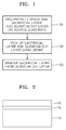
- FIG. 1 is a flowchart illustrating a method of manufacturing a quantum dot layer, according to an embodiment.
- a self-assembled monolayer (SAM), a sacrificial layer and a quantum dot layer are sequentially stacked on a source substrate 10 (S1).
- a surface treatment for forming, the SAM is performed on the source substrate 10 in advance so as to facilitate delamination of the sacrificial layer before forming the sacrificial layer.
- a material used to perform the surface treatment on the SAM may be a material for silanizing or fluorinating a surface of the source substrate 10.
- a surface treatment may be performed on a silicon substrate through solution dipping or thermal treatment using octadecyltrichlorosilane, octyltrichlorosilane, or trichloro(1H,1H,2H,2H-perfluorooctyl)silane and a derivative of the self-assembled material.
- the surface energy of the source substrate 10 may be greatly decreased, thereby facilitating delamination of the sacrificial layer.
- the sacrificial layer formed on the SAM may be a polymer-based material that may be easily generated/removed even at a low temperature, for example, in a temperature range of room temperature to 120 degrees Celsius.
- the sacrificial layer may be formed of a material, for example, polyethylene oxide (PEO), polyvinyl alcohol (PVAL), poly amic acid (PAA), polyvinylpyrrolidone (PVP), or polyvinylmethylether (PVME) (for example, alkyl- and peroxyl-type macroradicals) which is soluble in a polarizable solution.
- the molecular weight of a polymer used for forming the sacrificial layer may be in the range of from about 10,000 to about 500,000 g/mol.
- a quantum dot layer is formed on the sacrificial layer.
- the quantum dot layer may be formed on the sacrificial layer through a solution process.
- the quantum dot may be a Group II-IV quantum dot, a Group III-IV quantum dot, a Group V quantum dot, or a compound thereof.
- the quantum dot may include at least one selected from the group consisting of CdS, CdSe, CdTe, ZnS, ZnSe, ZnTe, HgS, HgSe, HgTe, GaN, GaP, GaAs, InP and InAs, but is not limited thereto.
- the quantum dot may include a compound including two or more materials selected from the group consisting of the above-stated materials.
- the compound may be a quantum dot compound including two or more quantum dots existing in a simply-mixed state, a mixed crystal in which two or more compound crystals are partially divided in the same crystal such as a crystal having a core-shell structure or a gradient structure, or a compound including two or more nanocrystals.
- the quantum dot may have a core structure in which holes may escape to the outside or a core/shell structure including a core and a shell covering the core.
- the core may include at least one material selected from the group consisting of CdSe, CdS, ZnS, ZnSe, CdTe, CdSeTe, CdZnS, PbSe, AglnZnS, and ZnO, but is not limited thereto.
- the shell may include at least one material selected from the group consisting of CdSe, ZnSe, ZnS, ZnTe, CdTe, PbS, TiO, SrSe, and HgSe, but embodiments are not limited thereto.
- the quantum dot may be manufactured using a quantum dot synthesizing method which is well known in the art.
- the quantum dot according to the present embodiment may include all quantum dots manufactured by a chemical wet method using a metallic precursor.
- the quantum dot may be manufactured using the method of injecting a predetermined metallic precursor into an organic solution included in a dispersant when necessary and growing the metallic precursor at a constant temperature, but embodiments are not limited thereto.
- a size of the quantum dot may be adjusted to absorb or emit light of red (R), green (G), and blue (B) wavelengths.
- the quantum dot may be coated on the sacrificial layer through a solution process, for example, by spin coating, deep coating, or spray coating, thereby forming a quantum dot layer.
- the quantum dot layer may be referred to as a quantum dot monolayer in which a plurality of quantum dots is arranged in a two-dimensional array.
- embodiments are not limited thereto, and the plurality of quantum dots may be arranged in a three-dimensional array.
- a stamp is disposed on the quantum dot layer, and the stamp picks up the sacrificial layer and the quantum dot layer through transfer printing (S2).
- the SAM formed on the source substrate 10 is coupled to the source substrate 10 by a covalent bond and functions to extremely reduce the surface energy.
- the stamp picks up the sacrificial layer the SAM and the sacrificial layer are separated from each other. Consequently, only the quantum dot and the sacrificial layer are transferred to the stamp.
- the sacrificial layer is removed using a solution that dissolves the sacrificial layer.
- the sacrificial layer may be immersed in a polarizable solution such as water or alcohol to remove the sacrificial layer from the quantum dot layer (S3).
- a polarizable solution such as water or alcohol
- an inorganic nanocrystal may be encapsulated by an organic ligand, and an organic capping layer is formed of an insulating material.
- the sacrificial layer is formed of a high molecular material which is soluble in a polarizable solution such as water or alcohol. Accordingly, even during the process of dissolving the sacrificial layer in the polarizable solution, the properties of the quantum dot layer do not change.
- the above-described quantum dot layer may be used as an active layer of an optoelectronic device such as a solar device or an emission device.
- an optoelectronic device such as a solar device or an emission device.
- a method of stacking the quantum dot layer on a device substrate will be described.
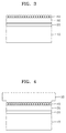
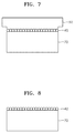
- FIGS. 2 to 8 are schematic views sequentially illustrating a method of manufacturing and transfer-printing a quantum dot layer, according to an embodiment.
- a SAM 20 and a sacrificial layer 30 are sequentially formed on a source substrate 10.
- the material for forming the SAM 20 may be a material for silanizing or fluorinating a surface of the source substrate 10.
- the sacrificial layer 30 may be a polymer-based material that may be easily generated/removed even at a low temperature, for example, in a range of room temperature (about 25 °C) to 120 degrees Celsius.
- the sacrificial layer 30 may be formed of a material which is soluble in a polarizable solution such as water.
- a quantum dot layer 40 is formed on the sacrificial layer 30 through, for example, a solution process.
- the quantum dot layer 40 may be formed by, for example, spin coating.
- the quantum dot layer 40 may be a quantum dot monolayer in which a plurality of quantum dots is arranged in a two-dimensional array.
- the quantum dot layer 40 is formed on the sacrificial layer 30, and then a stamp 50, for example, an elastomeric stamp, is disposed on the quantum dot layer 40 as illustrated in FIG. 4 . Then, the stamp 50 picks up the quantum dot layer 40 using a protruding portion of the stamp 50.
- the stamp 50 may be a siloxane-based, an acryl-based, or an epoxy-based elastic material or a composite thereof, or may be formed by mixing reinforced materials and adjusting an intensity of the materials.
- the stamp 50 may include, for example, soft-PDMS, hard-PDMS, polyurethaneacrylate, and the like, or may be an elastomeric polymer.
- a surface of the stamp 50 contacting the quantum dot layer 40 may be flat and may include a micro pattern.
- the stamp 50 may be manufactured to include the micro pattern.
- a mold of a desired pattern may be formed on a silicon wafer via photolithography using an SU8 (SU-8 photoresist) which is a negative photoresist (PR), and then a liquid high molecular weight material may be poured and cured on the mold, thereby completing a patterned elastomer.
- a surface treatment such as silanization or fluorination may be performed on the mold so as to easily separate the liquid high molecular material form the mold after performing the curing.
- the patterned elastomer is separated from the silicon wafer and then is cut to an appropriate size so as to be used as the patterned stamp.
- the patterned stamp 50 may easily pick up the quantum dot layer 40.
- the physical stress applied to the quantum dot layer 40, pressed to be picked up by the stamp 50, may be reduced, and also the pattern stamp 50 may closely contact the quantum dot layer 40, thereby easily picking up the quantum dot layer 40.
- an ultra-violet (UV)-ozone treatment may be performed on the stamp 50 so as to easily pick up the quantum dot layer 40. By performing the UV-ozone treatment, the surface energy of the stamp 50 is increased, thereby allowing it to more easily pick up the quantum dot layer 40.
- the quantum dot layer 40 contacting a protruding portion of the stamp 50 is picked up by the stamp 50. Then, when the quantum dot layer 40 is picked up, the sacrificial layer 30 is separated from the source substrate 10 and the SAM layer 20 to be picked up together with the quantum dot layer 40.
- the sacrificial layer 30 is removed from the quantum dot layer 40 using a solution 60 that dissolves the sacrificial layer 30.
- the sacrificial layer 30 may be immersed in a polarizable solution 60 so as to remove the sacrificial layer 30 from the quantum dot layer 40.
- the sacrificial layer 30 may be a polymer-based material that may be easily generated/removed even at a low temperature, for example, in a range of from room temperature to 120 degrees Celsius, and may be formed from a material which is soluble in the polarizable solution 60 such as water. Accordingly, in certain embodiments, if the sacrificial layer 30 is immersed in the polarizable solution 60, the sacrificial layer 30 dissolves in the polarizable solution 60 after a predetermined period of time.
- the quantum dot layer 40 may be transfer-printed on a device substrate 70. Then, as illustrated in FIG. 7 , the quantum dot layer 40 may be formed on the device substrate 70.
- the device substrate 70 is illustrated as a single-layer in FIG. 7 , the device substrate 70 may include any of variously stacked structures according to the type of a device in which the quantum dot layer 40 is used.
- the device substrate 70 may have a structure in which a transparent electrode, a hole injection layer (HIL), a hole transport layer (HTL), etc. are stacked.
- heat in a temperature range of from 30 degrees Celsius to 200 degrees Celsius may be applied to the quantum dot layer 40. More preferably, heat of around 70 degrees Celsius may be applied, such that the quantum dot layer 40 picked up by the stamp 50 is perfectly transferred onto the device substrate 70.
- the stamp 50 is separated from the quantum dot layer 40.
- a piezoelectric effect or micro-vibration such as acoustic waves, e.g. ultrasonic waves, may be applied so as to easily separate the quantum dots from the stamp 50.
- the patterned stamp 50 is structuralized to form micro patterns of from nano-scale to a scale of several micron in the stamp 50, thereby easily separating the quantum dots from the stamp 50 because of the small contact area therebetween.
- a multi-layered organic structure including the quantum dot layer 40 or the entire device may be easily transferred onto another substrate because of a small contact area between the multi-layered organic structure or the entire device and the stamp 50.
- the quantum dot layer 40 may be easily manufactured. Also, since the sacrificial layer 30 is used, the characteristics of the quantum dot layer 40 may be maintained and the quantum dot layer 40 may be printed over a large area. In addition, since the sacrificial layer 30 is used, a quantum dot layer may be printed regardless of the thickness of the quantum dot layer, ranging from a monolayer to a multi-layer thickness.
- FIG. 9 is a view illustrating a quantum dot optoelectronic device 100 manufactured using a method of manufacturing a quantum dot layer, according to an embodiment of the present disclosure, wherein FIG. 9 shows a quantum dot display.
- the quantum dot optoelectronic device 100 includes a substrate 71, a quantum dot active layer 80 formed using the above-described method of manufacturing a quantum dot layer, a first electrode 73, e.g. an anode, and a second electrode 93, e.g. a cathode, that are connected to an external power source so as to inject carriers (charge carriers) to the quantum dot active layer 80, a first charge transport layer, e.g. a HTL 77, disposed between the quantum dot active layer 80 and the first electrode 73, and a second charge transport layer, e.g. an electron transport layer (ETL) 91 disposed between the quantum dot active layer 80 and the second electrode 93.
- the quantum dot optoelectronic device 100 may further include a HIL 75 between the first electrode 73 and the HTL 77 that are formed on the substrate 71.
- the substrate 71 may be a transparent glass substrate or a flexible plastic substrate.
- the first electrode 73 may serve as an anode and may be formed of a material having a high work function so as to allow holes to be injected into the first electrode 73.
- the first electrode 73 may be formed of a transparent oxide such as indium tin oxide (ITO), indium oxide, or the like.
- ITO indium tin oxide
- the first electrode 73 may be formed on the substrate 71 through dry deposition such as sputtering.
- the HTL 77 is disposed between the first electrode 73 and the quantum dot active layer 80.
- the HTL 77 may be formed of a p-type semiconductor polymer, for example, PEDOT, PSS, PPV, PVK, or the like.
- the HTL 77 may be formed using a wet coating method such as spin coating.
- a precursor solution including a PPV precursor polymer and a methanol organic solvent is spin-coated on the first electrode 73, and thermal treatment is performed thereon in an inactive gas atmosphere or in a vacuum at a curing temperature of from 300 degrees Celsius to 750 degrees Celsius for three hours, thereby obtaining a HTL 77 formed of a PPV thin film.
- the quantum dot active layer 80 may be formed to realize a pixelized quantum dot display by transfer-printing quantum dot layers in which a plurality of colors are patterned, for example, quantum dot layers 81, 83, and 85 in which R, G, and B colors are patterned, onto the HTL 77 using the above-described method of manufacturing a quantum dot layer.
- Each quantum dot layer is a monolayer, and the plurality of quantum dot layers may be disposed spaced apart from one another.
- a quantum dot may have a diameter of from 1 nm to 10 nm.
- a quantum dot may have a homogeneous single-layer structure or a double-layer structure of a core-shell.
- materials for forming a core and a shell may be different semiconductor compounds described above.
- an energy band gap of the material for forming the shell may be greater than that of the material for forming the core.
- the ETL 91 is disposed between the quantum dot active layer 80 and the second electrode 93, that is, e.g., between cathodes, and may be formed of any of various materials.
- the material for forming the ETL 91 may be a metallic oxide such as TiO 2 , ZrO 2 , HfO 2 , or the like, an inorganic material including Si 3 N 4 , an n-type semiconductor polymer, or the like.
- the second electrode 93 may serve as a cathode and may be formed of a material having a small work function so as to allow electrons to be easily injected into the ETL 91.
- the second electrode 93 may be formed of one metal selected from the group consisting magnesium (Mg), calcium (Ca), sodium (Na), potassium (K), titanium (Ti), indium (In), yttrium (y), lithium (Li), gadolinium (Gd), aluminum (Al), silver (Ag), tin (Sn), lead (Pb), cesium (Cs), and barium (Ba), or an alloy thereof, or may be formed of a material having a multi-layered structure, for example, LiF/Al, LiO 2 /Al, LiF/Ca, LiF/Al, and BaF 2 /Ca, but embodiments are not limited thereto.
- the second electrode 93 may be formed through dry deposition such as sputtering.
- the second electrode 93 may be patterned in correspondence to the quantum dot active layer 80 having an array of the quantum dot layers 81, 83, and 85 in which R, G, and B colors are patterned so as to realize a pixelized quantum dot display.
- the HIL 75 may be disposed between the first electrode 73 and the HTL 77, and the material for forming the HIL 75 is not particularly limited. Any material having an excellent interfacial characteristic and capable of easily transmitting electrons to an electrode may be used to form the HIL 75.
- the HIL 75 may be formed of a material including poly(3,4-ethylenedioxythiophene) (PEDOT).
- a structure in which the first electrode 73, the HIL 75, the HTL 77, and the quantum dot active layer 80 are stacked on the substrate 71 is coupled to a structure in which the second electrode 93 and the ETL 91 are stacked, and light of R, G, and B colors are emitted through the substrate 71.
- this is just an example, and a quantum dot solar cell or a stacked structure of the quantum dot optoelectronic device 100 is not limited thereto.
- an ETL and a second electrode may be formed on a structure in which a first electrode, a HIL, a HTL, and a quantum dot active layer are stacked on a substrate, and solar light incident toward the second electrode may be absorbed into the quantum dot active layer or light of R, G, and B colors may exit.
- Light of one of the R, G, and B colors may be selectively emitted or light of each of the R, G, and B colors may be simultaneously emitted by differentiating their light intensities under control of a driving unit (not shown) so as to configure pixels of various colors.
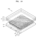
- R, G, and B quantum dot layers may be transfer-printed to be configured as a multi-layer as illustrated in FIG. 10 , thereby realizing an optoelectronic device such as a quantum dot (QD) solar cell or a quantum dot light-emitting device (QD-LED).
- QD quantum dot
- QD-LED quantum dot light-emitting device
- FIG. 10 is a view illustrating a quantum dot optoelectronic device 200 manufactured using a method of manufacturing a quantum dot layer according to another embodiment of the present disclosure.
- quantum dot active layer 80' is formed as a multi-layer including a plurality color quantum dot layers, for example, R, G, and B quantum dot layers 81, 83, and 85 and the quantum dot active layer 80' is not pixelized
- the basic stacked structure, material of each layer, and activation principle of the quantum dot optoelectronic device 200 illustrated in FIG. 10 are the same as those of the quantum dot optoelectronic device 100 illustrated in FIG. 9 .
- the same reference numerals as in FIG. 9 represent elements having substantially the same functions, and a duplicative description of the elements described with respect to FIG. 9 is not repeated here.
- the quantum dot may not be manufactured as a thin multi-layer.
- a sacrificial layer and R, G, and B quantum dot layers may be printed in a multi-layered structure on a device through transfer-printing and light of R, G, and B colors may be simultaneously emitted, thereby inducing white light-emission.
- white balance may be easily controlled using the thickness of each quantum dot layer and partial energy transfer between the quantum dot layers. As illustrated in FIG.
- carriers may sequentially cross unique energy barriers of the quantum dots of each quantum dot layer according to an order in which the quantum dot layers having various energy bands are disposed, thereby remarkably decreasing a threshold voltage and a driving voltage.
- a quantum dot emission layer having a multi-layered structure manufactured using the presently disclosed method of manufacturing a quantum dot layer white light may be controlled by partial energy transfer between quantum dot active layers and by controlling the thickness of each quantum dot active layer, thereby decreasing the driving voltage and increasing emission efficiency.
- each quantum dot active layer having a multi-layered structure absorbs light of various wavelengths so as to rapidly move generated and separated electrons and holes toward an electrode according to a gradational energy band structure, thereby increasing the light absorption and efficiency of a solar cell.
- the surface of the second substrate to be contacted with the first quantum dot layer comprises a second quantum dot layer.
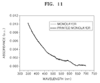
- the absorbance of the quantum dot layer is measured in order to check whether a loss of a characteristic of the quantum dot layer has occurred. For example, the absorbance of a quantum dot layer before and after the quantum dot layer is transferred onto a device substrate is measured, wherein the quantum dot layer has a thickness of 7 nm and includes a quantum dot solution of 0.23 wt%.
- FIG. 11 is a graph showing a result of the measurement of the absorbance of a quantum dot layer before and after being transferred, according to an embodiment of the present invention.
- the absorbance of the quantum dot layer before being transferred that is, the absorbance of the quantum dot layer formed on a sacrificial layer
- the absorbance of the quantum dot layer after being transferred that is, the absorbance of the quantum dot layer formed on a device substrate. Accordingly, FIG. 11 illustrates that the absorbance of the quantum dot layer is not influenced by the sacrificial layer.
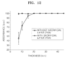
- FIG. 12 is a graph showing a result of the measurement of the pick-up yield of a quantum dot layer according to whether a sacrificial layer is used.
- the pick-up yield of the quantum dot layer having a thickness of less than 20 nm is remarkably decreased.
- the pick-up yield of the quantum dot layer having a thickness of less than 20 nm is high.
- FIG. 13 is a graph showing a result of the measurement of the photoluminescence (PL) intensities of a quantum dot layer having a single-layer structure and a quantum dot layer emitting a plurality of colors and having a multi-layered structure.
- the PL intensity when the quantum dot layer emits red light is the same as the PL intensity when the quantum dot layer having a multi-layered structure emits red and green light. Accordingly, FIG. 13 illustrates that even though the quantum dot layer has a multi-layered structure, a loss of the quantum dot layer does not occur during transfer-printing.
- the quantum dot layer is formed and transfer-printed using a sacrificial layer.
- the initial state of the quantum dot layer may be maintained without causing a loss of a characteristic of the quantum dot layer.
- the quantum dot layer may be configured as a multi-layered structure by repeatedly printing the quantum dot layer using the sacrificial layer, and also an optoelectronic device such as a large area solar device or an emission device may be easily manufactured.
- the quantum dot layer may have a high pick-up yield regardless of the thickness of the quantum dot layer, and thus quantum dot layers having various thicknesses may be transferred.
- a stamp picks up quantum dots cast on a source substrate to transfer-print the quantum dots onto a device substrate, and thus a quantum dot layer may be patterned to be a color pixel or quantum dot layers having various colors may be stacked in a multi-layered structure.
Claims (10)
- Verfahren zur Herstellung einer Quantenpunktschicht (40; 80; 80'), wobei das Verfahren Folgendes umfasst:das sequentielle Stapeln einer selbstzusammengebauten Monoschicht (SAM) (20), einer Opferschicht (30) und einer Quantenpunktschicht (40; 80; 80') auf einem Quellsubstrat (10);das Anordnen eines Stempels (50) auf der Quantenpunktschicht (40; 80; 80');das Aufnehmen der Opferschicht (30), der Quantenpunktschicht (40; 80; 80') und des Stempels (50) von der SAM (20); unddas Entfernen der Opferschicht (30) von der Quantenpunktschicht (40; 80; 80') unter der Verwendung einer Lösung (60), welche die Opferschicht (30) auflöst.
- Verfahren nach Anspruch 1, wobei die Quantenpunktschicht (40; 80; 80') auf der Opferschicht (30) durch einen Lösungsvorgang gebildet wird.
- Verfahren nach Anspruch 1 oder 2, wobei die Opferschicht (30) ein polymerbasiertes Material ist, das ein Molekulargewicht in dem Bereich von 10.000 bis 500.000 g/mol aufweist.
- Verfahren nach einem der Ansprüche 1-3, wobei die Quantenpunktschicht (40; 80; 80') eine Vielzahl von Quantenpunkten umfasst, die in einem zweidimensionalen Array angeordnet sind.
- Verfahren nach einem der Ansprüche 1-4, wobei der Stempel (50) ein elastomeres Polymer ist und wobei das Verfahren gegebenenfalls den zusätzlichen Schritt der Durchführung einer Ultraviolett-(UV)-Ozonbehandlung an dem Stempel (50) umfasst.
- Verfahren nach einem der Ansprüche 1-5, wobei eine Fläche des Stempels (50), welche die Quantenpunktschicht (40; 80; 80') berührt, Mikrostrukturen umfasst, die einen Kontaktbereich zwischen der Quantenpunktschicht (40; 80; 80') und dem Stempel (50) verkleinern.
- Verfahren nach einem der Ansprüche 1-6, ferner umfassend das Trennen des Stempels (50) von der Quantenpunktschicht (40; 80; 80') unter der Verwendung mindestens eines der Folgenden: Wärme, ein piezoelektrischer Effekt und Mikrovibration.
- Verfahren zur Übertragung einer ersten Quantenpunktschicht (40; 80; 80') von einem Substrat (10) zu einem anderen (70), wobei das Verfahren Folgendes umfasst:(a) das Herstellen der ersten Quantenpunktschicht (40; 80; 80') gemäß dem Verfahren nach einem der Ansprüche 1-7; und(b) das Ablagern der ersten Quantenpunktschicht (40; 80; 80') auf einem zweiten Substrat (70), wie etwa einem Vorrichtungssubstrat (70).
- Verfahren nach Anspruch 8, wobei im Anschluss an das sequentielle Stapeln ein Maß der Haftung zwischen der SAM (20) und der Opferschicht (30) niedriger ist als ein Maß der Haftung zwischen der Opferschicht (30) und der ersten Quantenpunktschicht (40; 80; 80').
- Verfahren nach Anspruch 8 oder 9, wobei eine Fläche des zweiten Substrats (70), die mit der ersten Quantenpunktschicht (80; 80') kontaktiert werden soll, eine zweite Quantenpunktschicht (81, 83, 85) umfasst.
Applications Claiming Priority (1)
| Application Number | Priority Date | Filing Date | Title |
|---|---|---|---|
| KR1020110090313A KR101822500B1 (ko) | 2011-09-06 | 2011-09-06 | 양자점층 제조 방법 및 양자점층을 포함한 양자점 광전자소자 |
Publications (3)
| Publication Number | Publication Date |
|---|---|
| EP2568337A2 EP2568337A2 (de) | 2013-03-13 |
| EP2568337A3 EP2568337A3 (de) | 2013-11-27 |
| EP2568337B1 true EP2568337B1 (de) | 2016-02-03 |
Family
ID=46690442
Family Applications (1)
| Application Number | Title | Priority Date | Filing Date |
|---|---|---|---|
| EP12181377.8A Active EP2568337B1 (de) | 2011-09-06 | 2012-08-22 | Verfahren zur Herstellung einer Quantenpunktschicht |
Country Status (5)
| Country | Link |
|---|---|
| US (1) | US8846418B2 (de) |
| EP (1) | EP2568337B1 (de) |
| JP (1) | JP6008663B2 (de) |
| KR (1) | KR101822500B1 (de) |
| CN (1) | CN102983230B (de) |
Cited By (1)
| Publication number | Priority date | Publication date | Assignee | Title |
|---|---|---|---|---|
| TWI632705B (zh) * | 2013-12-03 | 2018-08-11 | 皇家飛利浦有限公司 | 製造陶瓷透光屏障單元的方法、屏障單元、光源及照明器 |
Families Citing this family (39)
| Publication number | Priority date | Publication date | Assignee | Title |
|---|---|---|---|---|
| CN103412436B (zh) | 2013-07-24 | 2015-09-30 | 北京京东方光电科技有限公司 | 一种彩膜基板、液晶显示屏及单色量子点的分散方法 |
| JP2015156367A (ja) * | 2013-12-27 | 2015-08-27 | ザ・ボード・オブ・トラスティーズ・オブ・ザ・ユニバーシティ・オブ・イリノイ | ナノ構造材料積層体転移方法及びデバイス |
| JP6657956B2 (ja) * | 2014-01-16 | 2020-03-04 | コニカミノルタ株式会社 | 電界発光素子 |
| DE102014221525B4 (de) | 2014-05-16 | 2021-08-26 | Fraunhofer-Gesellschaft zur Förderung der angewandten Forschung e.V. | Messsystem |
| CN104157671B (zh) * | 2014-06-25 | 2018-02-23 | 京东方科技集团股份有限公司 | 一种电致发光显示面板、其制备方法及显示装置 |
| US10026913B2 (en) | 2014-11-28 | 2018-07-17 | Seoul National University R&Db Foundation | Quantum dot electronic device and quantum dot transfer printing method |
| US20170343712A1 (en) * | 2014-12-15 | 2017-11-30 | Merck Patent Gmbh | A polarized light emissive device |
| WO2016149043A1 (en) | 2015-03-13 | 2016-09-22 | Dow Global Technologies Llc | Nanostructure material methods and devices |
| KR102446410B1 (ko) | 2015-09-17 | 2022-09-22 | 삼성전자주식회사 | 광전소자 및 이를 포함하는 전자장치 |
| CN105304832B (zh) * | 2015-11-02 | 2017-07-25 | 深圳市华星光电技术有限公司 | 电致发光器件的制备方法 |
| EP3188260B1 (de) | 2015-12-31 | 2020-02-12 | Dow Global Technologies Llc | Nanostrukturmaterialstrukturen und verfahren |
| CN105514302B (zh) | 2016-01-26 | 2017-07-18 | 京东方科技集团股份有限公司 | 量子点发光二极管亚像素阵列、其制造方法以及显示装置 |
| CN105511155B (zh) * | 2016-02-22 | 2018-11-23 | 深圳市华星光电技术有限公司 | 量子点彩色滤光片的制造方法 |
| US10700236B2 (en) | 2016-03-17 | 2020-06-30 | Apple Inc. | Quantum dot spacing for high efficiency quantum dot LED displays |
| US9768404B1 (en) | 2016-03-17 | 2017-09-19 | Apple Inc. | Quantum dot spacing for high efficiency quantum dot LED displays |
| KR102651544B1 (ko) * | 2016-11-21 | 2024-03-28 | 삼성전자주식회사 | 광대역 다기능 광학소자와 그 제조 및 동작방법 |
| CN106531906A (zh) * | 2016-11-22 | 2017-03-22 | Tcl集团股份有限公司 | 一种量子点固态膜的转印方法与量子点转印系统 |
| CN106960913A (zh) * | 2017-03-31 | 2017-07-18 | 武汉华星光电技术有限公司 | 量子点发光二极管显示面板及其制备方法 |
| WO2018210142A1 (zh) * | 2017-05-19 | 2018-11-22 | 中国科学院化学研究所 | 一种打印激光光源的打印头模块、系统及方法 |
| KR102491856B1 (ko) * | 2017-12-18 | 2023-01-27 | 삼성전자주식회사 | 복수의 양자점층을 포함하는 광전 소자 |
| US10424614B2 (en) * | 2017-12-21 | 2019-09-24 | X Development Llc | Multi-color monolithic light-emitting diodes and methods for making the same |
| US10181495B1 (en) * | 2017-12-21 | 2019-01-15 | X Development Llc | Multi-color monolithic light-emitting diodes and methods for making the same |
| JP7330203B2 (ja) | 2018-03-30 | 2023-08-21 | コーニンクレッカ フィリップス エヌ ヴェ | 電力を自給する量子ドット放射線検出器モジュール |
| US11152536B2 (en) * | 2018-09-17 | 2021-10-19 | The Board Of Trustees Of The University Of Illinois | Photoresist contact patterning of quantum dot films |
| US11778843B2 (en) | 2018-09-18 | 2023-10-03 | Sharp Kabushiki Kaisha | Light-emitting device and manufacturing method of light-emitting device |
| WO2020059143A1 (ja) * | 2018-09-21 | 2020-03-26 | シャープ株式会社 | 発光素子、発光デバイス、及び発光素子の製造方法 |
| KR102655061B1 (ko) * | 2019-03-25 | 2024-04-09 | 삼성디스플레이 주식회사 | 양자점층 제조 방법, 양자점층을 포함하는 발광 소자 제조 방법, 및 양자점층을 포함하는 표시 장치 |
| KR102173550B1 (ko) * | 2019-06-11 | 2020-11-03 | 단국대학교 산학협력단 | 직접 전사법을 활용한 양자점 발광소자 제조방법 |
| KR20210034355A (ko) * | 2019-09-20 | 2021-03-30 | 삼성전자주식회사 | 전계 발광 소자 및 이를 포함하는 표시 장치 |
| CN110808262B (zh) * | 2019-11-15 | 2022-06-24 | 京东方科技集团股份有限公司 | 微型led显示器件及其制备方法 |
| US11121289B2 (en) | 2019-11-20 | 2021-09-14 | Tectus Corporation | Ultra-dense quantum dot color converters |
| WO2021250773A1 (ja) * | 2020-06-09 | 2021-12-16 | シャープ株式会社 | 発光素子及び表示装置 |
| CN112014993A (zh) * | 2020-09-14 | 2020-12-01 | 武汉华星光电技术有限公司 | 显示面板及其制备方法 |
| CN112993096B (zh) * | 2021-01-20 | 2023-01-17 | 中国石油大学(华东) | 一种单光子源集成器件加工方法 |
| CN113066948A (zh) * | 2021-03-18 | 2021-07-02 | 京东方科技集团股份有限公司 | 模具及其制备方法、转印方法 |
| WO2022222049A1 (zh) * | 2021-04-20 | 2022-10-27 | 京东方科技集团股份有限公司 | 量子点图案、量子点发光器件、显示装置及制作方法 |
| CN113359347B (zh) * | 2021-05-28 | 2022-12-23 | 深圳市华星光电半导体显示技术有限公司 | 一种量子点沉积装置 |
| CN113484941B (zh) * | 2021-07-09 | 2022-10-18 | 中国科学院半导体研究所 | 微透镜阵列耦合反射层结构制备方法 |
| CN114137660B (zh) * | 2021-11-29 | 2023-03-21 | 中国科学院上海微系统与信息技术研究所 | 一种混合集成光量子芯片的制备方法及其结构 |
Family Cites Families (6)
| Publication number | Priority date | Publication date | Assignee | Title |
|---|---|---|---|---|
| US7662659B2 (en) | 2004-08-04 | 2010-02-16 | Banpil Photonics, Inc. | Methods of forming arrays of nanoscale building blocks |
| KR20080074548A (ko) * | 2007-02-09 | 2008-08-13 | 삼성전자주식회사 | 양자점 발광 소자 및 이의 제조 방법 |
| DE102007016995A1 (de) | 2007-04-11 | 2008-10-16 | Beyer, André | Verfahren zum Übertragen einer Nanoschicht |
| KR101002683B1 (ko) * | 2008-08-19 | 2010-12-20 | 한국기계연구원 | 이중시트링과 릴리프밸브를 내장하는 고압력 볼밸브 |
| KR20100093858A (ko) | 2009-02-17 | 2010-08-26 | 삼성전자주식회사 | 양자점층 제조 방법 및 이를 적용하여 제조된 양자점 발광소자 |
| US8193010B2 (en) | 2009-06-29 | 2012-06-05 | Board Of Regents, The University Of Texas System | Uniform transfer of luminescent quantum dots onto a substrate |
-
2011
- 2011-09-06 KR KR1020110090313A patent/KR101822500B1/ko active IP Right Grant
-
2012
- 2012-05-29 US US13/482,274 patent/US8846418B2/en active Active
- 2012-08-22 EP EP12181377.8A patent/EP2568337B1/de active Active
- 2012-09-05 JP JP2012195400A patent/JP6008663B2/ja active Active
- 2012-09-06 CN CN201210328278.2A patent/CN102983230B/zh active Active
Cited By (1)
| Publication number | Priority date | Publication date | Assignee | Title |
|---|---|---|---|---|
| TWI632705B (zh) * | 2013-12-03 | 2018-08-11 | 皇家飛利浦有限公司 | 製造陶瓷透光屏障單元的方法、屏障單元、光源及照明器 |
Also Published As
| Publication number | Publication date |
|---|---|
| US8846418B2 (en) | 2014-09-30 |
| EP2568337A3 (de) | 2013-11-27 |
| CN102983230B (zh) | 2017-04-12 |
| EP2568337A2 (de) | 2013-03-13 |
| JP2013056412A (ja) | 2013-03-28 |
| CN102983230A (zh) | 2013-03-20 |
| KR20130026874A (ko) | 2013-03-14 |
| KR101822500B1 (ko) | 2018-01-29 |
| US20130056705A1 (en) | 2013-03-07 |
| JP6008663B2 (ja) | 2016-10-19 |
Similar Documents
| Publication | Publication Date | Title |
|---|---|---|
| EP2568337B1 (de) | Verfahren zur Herstellung einer Quantenpunktschicht | |
| KR20100093858A (ko) | 양자점층 제조 방법 및 이를 적용하여 제조된 양자점 발광소자 | |
| US7888857B2 (en) | Light emitting device with three-dimensional structure and fabrication method thereof | |
| KR100705181B1 (ko) | 나노 크기의 반구형 볼록부를 갖는 기판 또는 전극을이용한 고효율 유기 발광 소자 및 이의 제조 방법 | |
| US8581230B2 (en) | Light-emitting device having enhanced luminescence by using surface plasmon resonance and method of fabricating the same | |
| KR101775549B1 (ko) | 나노구조 물질 스택-전달 방법 및 장치 | |
| Kim et al. | Bright and stable quantum dots and their applications in full-color displays | |
| KR101140309B1 (ko) | 양자점 다층 박막을 포함한 전기발광소자 | |
| TWI440206B (zh) | 包含半導體奈米晶之發光元件 | |
| TWI515917B (zh) | 穩定且全溶液製程之量子點發光二極體 | |
| US9525151B2 (en) | Organic light emitting device | |
| KR101880596B1 (ko) | 양자점 또는 염료를 함유하는 대면적 필름 및 이의 제조 방법 | |
| KR20170108157A (ko) | 전자 엘리먼트 및 디스플레이 | |
| JP2009087754A (ja) | 発光素子 | |
| KR20120039940A (ko) | 양자점 발광장치 | |
| CN106784369A (zh) | 一种阵列结构量子点发光二极管器件及其制备方法 | |
| JP2021007074A (ja) | 電子デバイス及び電子デバイスの製造方法 | |
| CN108054285B (zh) | 量子点薄膜的制备方法、电致发光器件及其制备方法 | |
| CN105467749A (zh) | 纳米结构材料叠层转移方法和装置 | |
| CN113937230B (zh) | 一步法转印制备高性能的超高分辨qled | |
| Jiang | Surface and interface engineering in quantum dot and double-heterojunction nanorod light-emitting diodes | |
| Qasim et al. | 7.3: Influence of Layer Thickness on the Performance of Quantum Dots Light Emitting Devices |
Legal Events
| Date | Code | Title | Description |
|---|---|---|---|
| PUAI | Public reference made under article 153(3) epc to a published international application that has entered the european phase |
Free format text: ORIGINAL CODE: 0009012 |
|
| AK | Designated contracting states |
Kind code of ref document: A2 Designated state(s): AL AT BE BG CH CY CZ DE DK EE ES FI FR GB GR HR HU IE IS IT LI LT LU LV MC MK MT NL NO PL PT RO RS SE SI SK SM TR |
|
| AX | Request for extension of the european patent |
Extension state: BA ME |
|
| PUAL | Search report despatched |
Free format text: ORIGINAL CODE: 0009013 |
|
| AK | Designated contracting states |
Kind code of ref document: A3 Designated state(s): AL AT BE BG CH CY CZ DE DK EE ES FI FR GB GR HR HU IE IS IT LI LT LU LV MC MK MT NL NO PL PT RO RS SE SI SK SM TR |
|
| AX | Request for extension of the european patent |
Extension state: BA ME |
|
| RIC1 | Information provided on ipc code assigned before grant |
Ipc: B82Y 20/00 20110101ALI20131023BHEP Ipc: G03F 7/00 20060101AFI20131023BHEP |
|
| 17P | Request for examination filed |
Effective date: 20140331 |
|
| RBV | Designated contracting states (corrected) |
Designated state(s): AL AT BE BG CH CY CZ DE DK EE ES FI FR GB GR HR HU IE IS IT LI LT LU LV MC MK MT NL NO PL PT RO RS SE SI SK SM TR |
|
| RIC1 | Information provided on ipc code assigned before grant |
Ipc: G03F 7/00 20060101AFI20150513BHEP |
|
| GRAP | Despatch of communication of intention to grant a patent |
Free format text: ORIGINAL CODE: EPIDOSNIGR1 |
|
| INTG | Intention to grant announced |
Effective date: 20150720 |
|
| RIN1 | Information on inventor provided before grant (corrected) |
Inventor name: CHOI, BYOUNG-IYONG Inventor name: CHUNG, DAE-YOUNG Inventor name: CHO, KYUNG-SANG Inventor name: KIM, TAE-HO |
|
| GRAS | Grant fee paid |
Free format text: ORIGINAL CODE: EPIDOSNIGR3 |
|
| GRAA | (expected) grant |
Free format text: ORIGINAL CODE: 0009210 |
|
| AK | Designated contracting states |
Kind code of ref document: B1 Designated state(s): AL AT BE BG CH CY CZ DE DK EE ES FI FR GB GR HR HU IE IS IT LI LT LU LV MC MK MT NL NO PL PT RO RS SE SI SK SM TR |
|
| REG | Reference to a national code |
Ref country code: GB Ref legal event code: FG4D |
|
| REG | Reference to a national code |
Ref country code: AT Ref legal event code: REF Ref document number: 773957 Country of ref document: AT Kind code of ref document: T Effective date: 20160215 Ref country code: CH Ref legal event code: EP |
|
| REG | Reference to a national code |
Ref country code: IE Ref legal event code: FG4D |
|
| REG | Reference to a national code |
Ref country code: DE Ref legal event code: R096 Ref document number: 602012014311 Country of ref document: DE |
|
| REG | Reference to a national code |
Ref country code: LT Ref legal event code: MG4D Ref country code: NL Ref legal event code: MP Effective date: 20160203 |
|
| REG | Reference to a national code |
Ref country code: AT Ref legal event code: MK05 Ref document number: 773957 Country of ref document: AT Kind code of ref document: T Effective date: 20160203 |
|
| PG25 | Lapsed in a contracting state [announced via postgrant information from national office to epo] |
Ref country code: GR Free format text: LAPSE BECAUSE OF FAILURE TO SUBMIT A TRANSLATION OF THE DESCRIPTION OR TO PAY THE FEE WITHIN THE PRESCRIBED TIME-LIMIT Effective date: 20160504 Ref country code: ES Free format text: LAPSE BECAUSE OF FAILURE TO SUBMIT A TRANSLATION OF THE DESCRIPTION OR TO PAY THE FEE WITHIN THE PRESCRIBED TIME-LIMIT Effective date: 20160203 Ref country code: FI Free format text: LAPSE BECAUSE OF FAILURE TO SUBMIT A TRANSLATION OF THE DESCRIPTION OR TO PAY THE FEE WITHIN THE PRESCRIBED TIME-LIMIT Effective date: 20160203 Ref country code: IT Free format text: LAPSE BECAUSE OF FAILURE TO SUBMIT A TRANSLATION OF THE DESCRIPTION OR TO PAY THE FEE WITHIN THE PRESCRIBED TIME-LIMIT Effective date: 20160203 Ref country code: HR Free format text: LAPSE BECAUSE OF FAILURE TO SUBMIT A TRANSLATION OF THE DESCRIPTION OR TO PAY THE FEE WITHIN THE PRESCRIBED TIME-LIMIT Effective date: 20160203 Ref country code: NO Free format text: LAPSE BECAUSE OF FAILURE TO SUBMIT A TRANSLATION OF THE DESCRIPTION OR TO PAY THE FEE WITHIN THE PRESCRIBED TIME-LIMIT Effective date: 20160503 |
|
| REG | Reference to a national code |
Ref country code: FR Ref legal event code: PLFP Year of fee payment: 5 |
|
| PG25 | Lapsed in a contracting state [announced via postgrant information from national office to epo] |
Ref country code: RS Free format text: LAPSE BECAUSE OF FAILURE TO SUBMIT A TRANSLATION OF THE DESCRIPTION OR TO PAY THE FEE WITHIN THE PRESCRIBED TIME-LIMIT Effective date: 20160203 Ref country code: IS Free format text: LAPSE BECAUSE OF FAILURE TO SUBMIT A TRANSLATION OF THE DESCRIPTION OR TO PAY THE FEE WITHIN THE PRESCRIBED TIME-LIMIT Effective date: 20160603 Ref country code: LT Free format text: LAPSE BECAUSE OF FAILURE TO SUBMIT A TRANSLATION OF THE DESCRIPTION OR TO PAY THE FEE WITHIN THE PRESCRIBED TIME-LIMIT Effective date: 20160203 Ref country code: SE Free format text: LAPSE BECAUSE OF FAILURE TO SUBMIT A TRANSLATION OF THE DESCRIPTION OR TO PAY THE FEE WITHIN THE PRESCRIBED TIME-LIMIT Effective date: 20160203 Ref country code: PT Free format text: LAPSE BECAUSE OF FAILURE TO SUBMIT A TRANSLATION OF THE DESCRIPTION OR TO PAY THE FEE WITHIN THE PRESCRIBED TIME-LIMIT Effective date: 20160603 Ref country code: PL Free format text: LAPSE BECAUSE OF FAILURE TO SUBMIT A TRANSLATION OF THE DESCRIPTION OR TO PAY THE FEE WITHIN THE PRESCRIBED TIME-LIMIT Effective date: 20160203 Ref country code: AT Free format text: LAPSE BECAUSE OF FAILURE TO SUBMIT A TRANSLATION OF THE DESCRIPTION OR TO PAY THE FEE WITHIN THE PRESCRIBED TIME-LIMIT Effective date: 20160203 Ref country code: NL Free format text: LAPSE BECAUSE OF FAILURE TO SUBMIT A TRANSLATION OF THE DESCRIPTION OR TO PAY THE FEE WITHIN THE PRESCRIBED TIME-LIMIT Effective date: 20160203 Ref country code: LV Free format text: LAPSE BECAUSE OF FAILURE TO SUBMIT A TRANSLATION OF THE DESCRIPTION OR TO PAY THE FEE WITHIN THE PRESCRIBED TIME-LIMIT Effective date: 20160203 |
|
| PG25 | Lapsed in a contracting state [announced via postgrant information from national office to epo] |
Ref country code: DK Free format text: LAPSE BECAUSE OF FAILURE TO SUBMIT A TRANSLATION OF THE DESCRIPTION OR TO PAY THE FEE WITHIN THE PRESCRIBED TIME-LIMIT Effective date: 20160203 Ref country code: EE Free format text: LAPSE BECAUSE OF FAILURE TO SUBMIT A TRANSLATION OF THE DESCRIPTION OR TO PAY THE FEE WITHIN THE PRESCRIBED TIME-LIMIT Effective date: 20160203 |
|
| REG | Reference to a national code |
Ref country code: DE Ref legal event code: R097 Ref document number: 602012014311 Country of ref document: DE |
|
| PG25 | Lapsed in a contracting state [announced via postgrant information from national office to epo] |
Ref country code: RO Free format text: LAPSE BECAUSE OF FAILURE TO SUBMIT A TRANSLATION OF THE DESCRIPTION OR TO PAY THE FEE WITHIN THE PRESCRIBED TIME-LIMIT Effective date: 20160203 Ref country code: SK Free format text: LAPSE BECAUSE OF FAILURE TO SUBMIT A TRANSLATION OF THE DESCRIPTION OR TO PAY THE FEE WITHIN THE PRESCRIBED TIME-LIMIT Effective date: 20160203 Ref country code: SM Free format text: LAPSE BECAUSE OF FAILURE TO SUBMIT A TRANSLATION OF THE DESCRIPTION OR TO PAY THE FEE WITHIN THE PRESCRIBED TIME-LIMIT Effective date: 20160203 Ref country code: CZ Free format text: LAPSE BECAUSE OF FAILURE TO SUBMIT A TRANSLATION OF THE DESCRIPTION OR TO PAY THE FEE WITHIN THE PRESCRIBED TIME-LIMIT Effective date: 20160203 |
|
| PLBE | No opposition filed within time limit |
Free format text: ORIGINAL CODE: 0009261 |
|
| STAA | Information on the status of an ep patent application or granted ep patent |
Free format text: STATUS: NO OPPOSITION FILED WITHIN TIME LIMIT |
|
| PG25 | Lapsed in a contracting state [announced via postgrant information from national office to epo] |
Ref country code: BE Free format text: LAPSE BECAUSE OF FAILURE TO SUBMIT A TRANSLATION OF THE DESCRIPTION OR TO PAY THE FEE WITHIN THE PRESCRIBED TIME-LIMIT Effective date: 20160203 |
|
| 26N | No opposition filed |
Effective date: 20161104 |
|
| PG25 | Lapsed in a contracting state [announced via postgrant information from national office to epo] |
Ref country code: BG Free format text: LAPSE BECAUSE OF FAILURE TO SUBMIT A TRANSLATION OF THE DESCRIPTION OR TO PAY THE FEE WITHIN THE PRESCRIBED TIME-LIMIT Effective date: 20160503 Ref country code: SI Free format text: LAPSE BECAUSE OF FAILURE TO SUBMIT A TRANSLATION OF THE DESCRIPTION OR TO PAY THE FEE WITHIN THE PRESCRIBED TIME-LIMIT Effective date: 20160203 |
|
| PG25 | Lapsed in a contracting state [announced via postgrant information from national office to epo] |
Ref country code: MC Free format text: LAPSE BECAUSE OF FAILURE TO SUBMIT A TRANSLATION OF THE DESCRIPTION OR TO PAY THE FEE WITHIN THE PRESCRIBED TIME-LIMIT Effective date: 20160203 |
|
| REG | Reference to a national code |
Ref country code: CH Ref legal event code: PL |
|
| PG25 | Lapsed in a contracting state [announced via postgrant information from national office to epo] |
Ref country code: LI Free format text: LAPSE BECAUSE OF NON-PAYMENT OF DUE FEES Effective date: 20160831 Ref country code: CH Free format text: LAPSE BECAUSE OF NON-PAYMENT OF DUE FEES Effective date: 20160831 |
|
| REG | Reference to a national code |
Ref country code: IE Ref legal event code: MM4A |
|
| REG | Reference to a national code |
Ref country code: FR Ref legal event code: PLFP Year of fee payment: 6 |
|
| PG25 | Lapsed in a contracting state [announced via postgrant information from national office to epo] |
Ref country code: IE Free format text: LAPSE BECAUSE OF NON-PAYMENT OF DUE FEES Effective date: 20160822 |
|
| PG25 | Lapsed in a contracting state [announced via postgrant information from national office to epo] |
Ref country code: LU Free format text: LAPSE BECAUSE OF NON-PAYMENT OF DUE FEES Effective date: 20160822 |
|
| PG25 | Lapsed in a contracting state [announced via postgrant information from national office to epo] |
Ref country code: HU Free format text: LAPSE BECAUSE OF FAILURE TO SUBMIT A TRANSLATION OF THE DESCRIPTION OR TO PAY THE FEE WITHIN THE PRESCRIBED TIME-LIMIT; INVALID AB INITIO Effective date: 20120822 Ref country code: CY Free format text: LAPSE BECAUSE OF FAILURE TO SUBMIT A TRANSLATION OF THE DESCRIPTION OR TO PAY THE FEE WITHIN THE PRESCRIBED TIME-LIMIT Effective date: 20160203 |
|
| PG25 | Lapsed in a contracting state [announced via postgrant information from national office to epo] |
Ref country code: MK Free format text: LAPSE BECAUSE OF FAILURE TO SUBMIT A TRANSLATION OF THE DESCRIPTION OR TO PAY THE FEE WITHIN THE PRESCRIBED TIME-LIMIT Effective date: 20160203 Ref country code: TR Free format text: LAPSE BECAUSE OF FAILURE TO SUBMIT A TRANSLATION OF THE DESCRIPTION OR TO PAY THE FEE WITHIN THE PRESCRIBED TIME-LIMIT Effective date: 20160203 Ref country code: MT Free format text: LAPSE BECAUSE OF NON-PAYMENT OF DUE FEES Effective date: 20160831 |
|
| REG | Reference to a national code |
Ref country code: FR Ref legal event code: PLFP Year of fee payment: 7 |
|
| PG25 | Lapsed in a contracting state [announced via postgrant information from national office to epo] |
Ref country code: AL Free format text: LAPSE BECAUSE OF FAILURE TO SUBMIT A TRANSLATION OF THE DESCRIPTION OR TO PAY THE FEE WITHIN THE PRESCRIBED TIME-LIMIT Effective date: 20160203 |
|
| P01 | Opt-out of the competence of the unified patent court (upc) registered |
Effective date: 20230520 |
|
| PGFP | Annual fee paid to national office [announced via postgrant information from national office to epo] |
Ref country code: GB Payment date: 20230720 Year of fee payment: 12 |
|
| PGFP | Annual fee paid to national office [announced via postgrant information from national office to epo] |
Ref country code: FR Payment date: 20230721 Year of fee payment: 12 Ref country code: DE Payment date: 20230718 Year of fee payment: 12 |