EP2565902A2 - Elektronenstrahl-Belichtungssystem - Google Patents
Elektronenstrahl-Belichtungssystem Download PDFInfo
- Publication number
- EP2565902A2 EP2565902A2 EP12188366A EP12188366A EP2565902A2 EP 2565902 A2 EP2565902 A2 EP 2565902A2 EP 12188366 A EP12188366 A EP 12188366A EP 12188366 A EP12188366 A EP 12188366A EP 2565902 A2 EP2565902 A2 EP 2565902A2
- Authority
- EP
- European Patent Office
- Prior art keywords
- beamlet
- array
- electron
- beamlets
- electron beam
- Prior art date
- Legal status (The legal status is an assumption and is not a legal conclusion. Google has not performed a legal analysis and makes no representation as to the accuracy of the status listed.)
- Withdrawn
Links
Images




Classifications
-
- H—ELECTRICITY
- H01—ELECTRIC ELEMENTS
- H01J—ELECTRIC DISCHARGE TUBES OR DISCHARGE LAMPS
- H01J37/00—Discharge tubes with provision for introducing objects or material to be exposed to the discharge, e.g. for the purpose of examination or processing thereof
- H01J37/30—Electron-beam or ion-beam tubes for localised treatment of objects
- H01J37/302—Controlling tubes by external information, e.g. program control
-
- H—ELECTRICITY
- H01—ELECTRIC ELEMENTS
- H01J—ELECTRIC DISCHARGE TUBES OR DISCHARGE LAMPS
- H01J3/00—Details of electron-optical or ion-optical arrangements common to two or more basic types of discharge tubes or lamps
- H01J3/02—Electron guns
-
- B—PERFORMING OPERATIONS; TRANSPORTING
- B82—NANOTECHNOLOGY
- B82Y—SPECIFIC USES OR APPLICATIONS OF NANOSTRUCTURES; MEASUREMENT OR ANALYSIS OF NANOSTRUCTURES; MANUFACTURE OR TREATMENT OF NANOSTRUCTURES
- B82Y10/00—Nanotechnology for information processing, storage or transmission, e.g. quantum computing or single electron logic
-
- B—PERFORMING OPERATIONS; TRANSPORTING
- B82—NANOTECHNOLOGY
- B82Y—SPECIFIC USES OR APPLICATIONS OF NANOSTRUCTURES; MEASUREMENT OR ANALYSIS OF NANOSTRUCTURES; MANUFACTURE OR TREATMENT OF NANOSTRUCTURES
- B82Y40/00—Manufacture or treatment of nanostructures
-
- H—ELECTRICITY
- H01—ELECTRIC ELEMENTS
- H01J—ELECTRIC DISCHARGE TUBES OR DISCHARGE LAMPS
- H01J37/00—Discharge tubes with provision for introducing objects or material to be exposed to the discharge, e.g. for the purpose of examination or processing thereof
- H01J37/02—Details
- H01J37/04—Arrangements of electrodes and associated parts for generating or controlling the discharge, e.g. electron-optical arrangement or ion-optical arrangement
- H01J37/06—Electron sources; Electron guns
-
- H—ELECTRICITY
- H01—ELECTRIC ELEMENTS
- H01J—ELECTRIC DISCHARGE TUBES OR DISCHARGE LAMPS
- H01J37/00—Discharge tubes with provision for introducing objects or material to be exposed to the discharge, e.g. for the purpose of examination or processing thereof
- H01J37/30—Electron-beam or ion-beam tubes for localised treatment of objects
- H01J37/304—Controlling tubes by information coming from the objects or from the beam, e.g. correction signals
-
- H—ELECTRICITY
- H01—ELECTRIC ELEMENTS
- H01J—ELECTRIC DISCHARGE TUBES OR DISCHARGE LAMPS
- H01J37/00—Discharge tubes with provision for introducing objects or material to be exposed to the discharge, e.g. for the purpose of examination or processing thereof
- H01J37/30—Electron-beam or ion-beam tubes for localised treatment of objects
- H01J37/317—Electron-beam or ion-beam tubes for localised treatment of objects for changing properties of the objects or for applying thin layers thereon, e.g. for ion implantation
-
- H—ELECTRICITY
- H01—ELECTRIC ELEMENTS
- H01J—ELECTRIC DISCHARGE TUBES OR DISCHARGE LAMPS
- H01J37/00—Discharge tubes with provision for introducing objects or material to be exposed to the discharge, e.g. for the purpose of examination or processing thereof
- H01J37/30—Electron-beam or ion-beam tubes for localised treatment of objects
- H01J37/317—Electron-beam or ion-beam tubes for localised treatment of objects for changing properties of the objects or for applying thin layers thereon, e.g. for ion implantation
- H01J37/3174—Particle-beam lithography, e.g. electron beam lithography
- H01J37/3177—Multi-beam, e.g. fly's eye, comb probe
-
- H—ELECTRICITY
- H01—ELECTRIC ELEMENTS
- H01J—ELECTRIC DISCHARGE TUBES OR DISCHARGE LAMPS
- H01J2237/00—Discharge tubes exposing object to beam, e.g. for analysis treatment, etching, imaging
- H01J2237/04—Means for controlling the discharge
- H01J2237/043—Beam blanking
- H01J2237/0435—Multi-aperture
-
- H—ELECTRICITY
- H01—ELECTRIC ELEMENTS
- H01J—ELECTRIC DISCHARGE TUBES OR DISCHARGE LAMPS
- H01J2237/00—Discharge tubes exposing object to beam, e.g. for analysis treatment, etching, imaging
- H01J2237/06—Sources
- H01J2237/063—Electron sources
- H01J2237/06308—Thermionic sources
-
- H—ELECTRICITY
- H01—ELECTRIC ELEMENTS
- H01J—ELECTRIC DISCHARGE TUBES OR DISCHARGE LAMPS
- H01J2237/00—Discharge tubes exposing object to beam, e.g. for analysis treatment, etching, imaging
- H01J2237/06—Sources
- H01J2237/063—Electron sources
- H01J2237/06375—Arrangement of electrodes
-
- H—ELECTRICITY
- H01—ELECTRIC ELEMENTS
- H01J—ELECTRIC DISCHARGE TUBES OR DISCHARGE LAMPS
- H01J2237/00—Discharge tubes exposing object to beam, e.g. for analysis treatment, etching, imaging
- H01J2237/30—Electron or ion beam tubes for processing objects
- H01J2237/304—Controlling tubes
- H01J2237/30433—System calibration
- H01J2237/3045—Deflection calibration
Definitions
- a conventional electron beam exposure apparatus has a throughput of about 1/100 wafer/hr. However, for lithography purposes a commercially acceptable throughput of at least a few wafers/hr is necessary. Several ideas to increase the throughput of an electron beam exposure apparatus have been proposed.
- US-A1-5.760.410 and US-A1-6.313.476 disclose a lithography system using an electron beam having a cross section, which is modified during the transferring of a pattern to an exposure surface of a target.
- the specific cross section or shape of the beam is established during operation by moving the emitted beam inside an aperture by using electrostatic deflection.
- the selected aperture partially blanks and thereby shapes the electron beam.
- the target exposure surface moves under the beam to refresh the surface. In this way a pattern is written.
- the throughput of this system is still limited.
- an electron beam lithography system using a plurality of electron beams by using a plurality of continuous wave (CW) emitters to generate a plurality of electron beamlets. Each beamlet is then individually shaped and blanked to create a pattern on the underlying substrate. As all these emitters have slightly different emission characteristics, homogeneity of the beamlets is a problem. This was corrected by levelling every individual beam current to a reference current. Correction values for the mismatch are extremely difficult to calculate and it takes a significant amount of time, which reduces the throughput of the system.
- CW continuous wave
- a system which uses one LaB 6 -source for generating one electron beam, which is subsequently, expands, collimated and split into a plurality of beamlets.
- the target exposure surface is mechanically moved relatively to the plurality of beamlets in a first direction, the beamlets are switched on and off using blanking electrostatic deflectors and at the same time scanning deflectors sweep the beamlets which have passed the blanker array over the target exposure surface in a direction perpendicular to the first direction, thus each time creating an image.
- electrostatic and/or magnetic lenses are used to reduce the image before it is projected on the target exposure surface.
- At least one complete intermediate image is created, smaller than the one before.
- the entire image has the desired dimensions, it is projected on the target exposure surface.
- a major disadvantage of this approach is that the plurality of electron beamlets together has to pass through at least one complete crossover. In this crossover, Coulomb interactions between electron in different beamlets will disturb the image, thus reducing the resolution.
- the area that is exposed at one time is rather small, so a lot of wafer scans are needed to expose a die: 16 scans are needed to expose one die, requiring a very high stage speed for reaching a commercially acceptable throughput.
- a multibeam particle lithography system having an illumination system, which produces a plurality of ion sub-beams.
- the illumination systems use either a single ion source with aperture plates for splitting a beam in sub-beams, or a plurality of sources.
- the aperture plate is projected (demagnified) on a substrate using a multibeam optical system.
- the system furthermore uses a deflection unit of electrostatic multipole systems, positioned after the multibeam optical system, for correcting individual imaging aberrations of a sub-beam and positioning the sub-beam during writing.
- the publication does not disclose how each sub-beam is modulated. Furthermore, controlling individual sub-beams is a problem, and maintaining inter-sub-beam uniformity.
- a multi-electron beam ('probes') lithography system having a specific ZrO/W-TFE thermal emission source with an emitter tip immersed in a magnetic field.
- a disadvantage of such a source is its limited output. Furthermore, this source needs a crossover. The mutual homogeneity of the 'probes' is not further discussed. Furthermore, the intensity of the source is a problem
- the article furthermore in a general way mentions a writing strategy in which a stage is moved in one direction, and deflectors move the 'probes' concurrently through the same distance perpendicular to the direction of the stage movement.
- a further problem, not recognised in this publication, is correction of deviation of electron beamlets from their intended positions.
- Another objective is to improve the resolution of known electron beam exposure apparatus.
- Yet another objective of the current invention is to improve throughput of known electron beam exposure apparatus.
- Yet another objective of the current invention is to overcome the problems related to Coulomb interactions and the demagnification methods in the prior art.
- Another objective of the current invention is to simplify controlling uniformity of beamlets, especially during writing.
- the invention relates to a maskless lithography system for transferring a pattern onto the surface of a target according to claim 1.
- said modulation array comprises:
- substantially every beamlet blanker is aligned with an electron beamlet, in order to make it possible to individually modulate every beamlet.
- the beamlet stop array comprises at least one plane of apertures, substantially every aperture being aligned with one beamlet, preferably with an aperture centred with respect to a beamlet. In this way, a beamlet passes an aperture when an electron beamlet is not deflected, and a beamlet is blocked or stopped when the beamlet is deflected.
- the controller is operationally connected to said beamlet blankers.
- the electron beam exposure apparatus is furthermore provided with measuring means for measuring the actual position of at least one of said beamlets
- the controller is provided with memory means for storing said actual position and a desired position, a comparator for comparing the desired position and the actual position of said beamlets, and wherein the adjustor is operationally connected to the controller for receiving instructions for adjusting the control signals issued to the modulators to compensate for the measured difference between said desired position and said actual position of said electron beamlets.
- the adjustor is operationally connected to the controller for receiving instructions for adjusting the control signals issued to the modulators to compensate for the measured difference between said desired position and said actual position of said electron beamlets.
- the controller is operationally connected to the beamlet blankers, in an embodiment via the adjustor.
- the adjustor is operationally connected to the controller for receiving instructions indicating the amount of the adjustments.
- the amount of the adjustments can be determined based a resulting value of the above-mentioned comparator.
- the adjustor is adapted for individually adjusting timing of each control signal. In this very easy way, correction can be accomplished.
- the beamlet generating means comprise:
- the electron beam exposure apparatus further comprising a second electrostatic lens array located between said beam splitting means and said beamlet blanker array to focus said plurality of electron beamlets.
- substantially every electrostatic lens is aligned and focuses one electron beamlet.
- the beamlet blanker array is located in the focal plane of said second electrostatic lens array.
- the beamsplitter comprise a spatial filter, preferably an aperture array.
- a spatial filter preferably an aperture array.
- the splitting means can comprise a number of aperture arrays in a serial order along the path of the electron beam or plurality of beamlets, the aperture arrays having mutually aligned apertures, each next aperture array along the path from the source to the target having apertures that are smaller than the apertures of the previous aperture array. This reduces heat load.
- the apertures of each aperture array are arranged in a hexagonal structure, which makes it possible to obtain close integration.
- each aperture of the aperture array has an area inversely proportional to the current density based on the beamlet that is transmitted through that same aperture.
- the beamsplitter comprises an aperture array, wherein the aperture sizes in the aperture array are adapted to create a discrete set of predetermined beamlet currents.
- the beamsplitter comprises an electrostatic quadrupole lens array.
- the electron beam exposure apparatus comprises a thermionic source.
- the thermionic source is adapted for being operated in the space charge limited regime. It was found that space charge has a homogenising effect, which is favourable in this specific application. Furthermore, in certain settings, the space charge may have a negative lens effect.
- the thermionic electron source has a spherical cathode surface.
- the thermionic source comprises at least one extractor electrode.
- the extractor electrode is a planar extractor electrode.
- the extractor is located after the space charge region and provided with a positive voltage for inducing a negative lens effect. These voltages can be set at a predefined value for creating a negative lens effect for the emitted electron beam.
- the extractor electrode has a spherical surface with through holes. All these embodiments serve to create a negative lens influence on the electron beam, thus avoiding a crossover in the electron beam.
- the apparatus further comprises an illumination system that transforms the electron beam, emitted by said source, into a collimated electron beam before it reaches said splitting means.
- said beamlet generator comprises an array of sources of which each source is responsible for the generation of an electron beamlet.
- the electron beam exposure apparatus further comprising a second electrostatic lens array located between said array of sources and said beamlet blanker array to focus said plurality of electron beamlets.
- said beamlet blanker comprise electrostatic deflectors.
- the electron beam exposure apparatus further comprising scanning deflection means provided between the modulation array and the focusing electron optical system for deflecting the electron beamlets to scan said target exposure surface.
- the scanning deflection means comprises electrostatic scan deflectors.
- the electron beam exposure apparatus is further provided with actuating means for moving said electrostatic scan deflectors and said means for holding the target relatively to each other in the plane of the surface onto which the pattern is to be transferred in a direction that differs from the direction of the deflection performed by said electrostatic scan deflectors.
- the adjustor or a time shifter are adapted for shifting a timing base of the scanning deflection means and the actuators with respect to each other.
- the control signals of the modulators have a timing base and the actuators of the target holder have a second timing base, and there timing bases can be shifted with respect to one another. This can for instance be used to have a critical component, which has to be written on the target surface and which would lay between two beamlets, written using only one beamlet.
- the electron beam exposure apparatus furthermore comprises an additional aperture plate between the modulation array and the focussing electron optical system, the additional aperture plate having one surface directed to and substantially parallel to the exposure surface of the target, wherein said electrostatic scan deflectors are conducting strips deposited on the side of the additional aperture plate facing the exposure surface of the target located between said blanker array and the electrostatic lens array of the focusing electron optical system.
- the electrostatic scan deflectors are conducting strips deposited at the target exposure surface side of any of the lens plates present in the focusing electron optical system.
- the conducting strips alternatively have a positive or negative potential.
- these deflectors deflect the electron beamlets in such a way that a predetermined section of the beamlet is stopped by the beamlet stop array.
- the electron beam exposure apparatus further comprises a post-reduction acceleration stage, located between the electrostatic lens array of the focusing electron optical system and said protective means, for accelerating the electrons in the plurality of transmitted electron beamlets
- controller it is furthermore provided with correction means to compensate for the incorrect positioning of the electron beamlets on the target exposure surface by
- the electron beam exposure apparatus further comprising protective means to prevent particles released by impinging electrons to reach any one of the aperture arrays, lens arrays or blanker arrays, preferably located between the electrostatic lens array of the focusing electron optical system and the exposure surface of a target, preferably comprising an aperture array wherein the apertures have a size smaller than 20 ⁇ m.
- all lens arrays, aperture arrays and blanker arrays are connected to a power supply, which, when gas is admitted into the system, creates a plasma that cleans the plates and removes all contaminants.
- the electron beam exposure apparatus the system is operated at an elevated temperature of about 200-600 °C to keep the apparatus clean.
- An electron beam exposure apparatus for transferring a pattern onto the surface of a target may comprise:
- said extractor electrode is located after said space charge region and is provided with a positive voltage for inducing a negative lens effect to said electron beam.
- An electron beam generator for generating a plurality of electron beamlets may comprise at least one thermionic source, said source comprising at least one extractor electrode adapted for being operated in a space charge limited region, said source adapted for generating an electron beam, and said beamlet generator furthermore provided with a beamsplitter for splitting said electron beam up into a plurality of electron beamlets.
- An electron beam exposure apparatus for transferring a pattern onto the surface of a target may comprise a beamlet generator for generating a plurality of electron beamlets, a plurality of modulators for modulating each electron beamlet, and a controller for providing each modulator with a control signal, said control signal having a timing base, wherein the controller is adapted for individually adjusting the timing base of a control signal with respect to the other control signals.
- a method for transferring a pattern onto a target exposure surface with an electron beam is described, using an electron beam exposure apparatus described above, and to a wafer processed using the apparatus of the current invention.
- the apparatus can furthermore be used for the production of mask, like for instance used in state-of-the-art optical lithography systems.
- FIGURE 1 An embodiment of the present invention is schematically shown in FIGURE 1 . Electrons are emitted from a single, stable electron source 1.
- An illumination system focuses and collimates the emitted electron beam 5 to illuminate a desired area on an aperture plate 6 uniformly. This can for instance be established by using lenses 3 and 4. Due to the aperture plate 6 the electron beam 5 is split in a plurality of electron beamlets, two of which 5a and 5b, are shown.
- An alternative way to create a plurality of electron beamlets is to use an array of electron sources. Each electron source generates an electron beamlet, which is modulated in the same way as the one created with a combination of a single source and splitting means. Since the emission characteristics of each source are slightly different, a single source 1 with beamsplitter 6 is preferred.
- An array of electrostatic lenses 7 focuses each beamlet to a desired diameter.
- a beamlet blanker array 8 is positioned in such a way that each individual beamlet coincides with an aperture in the plate of beamlet blanker array 8.
- the beamlet blanker array 8 comprises beamlet-blankers, for instance blanking electrostatic deflectors. When a voltage is applied on a blanking deflector an electric field across the corresponding aperture is established.
- the passing electron beamlet for example beamlet 9, deflects and terminates at the beamlet stop array 10, located behind the beamlet blanker array 8 following the electron beamlet trajectory. When there is no voltage applied to the blanking deflector the electron beamlet will pass the beamlet stop array 10, and reach the focusing electron optical system comprising an array of electrostatic lenses 13.
- This array 13 focuses each of the transmitted beamlets 12 individually on the target exposure surface 14.
- scanning deflection means most often electrostatic scan deflectors, move the beamlets together in one direction over the target exposure surface 14.
- the scan deflectors are located on the target exposure surface side 11a of beamlet stop array 10, thus forming an additional scan deflection array 11.
- other locations are also possible.
- the target exposure surface 14 and the scan deflectors moves relatively to one another in a direction different from the direction of the scan deflection.
- the target is a wafer or a mask covered with a resist layer.
- FIGURE 1 A remarkable aspect of the configuration shown in FIGURE 1 is that the entire image that is created by the combination of beamlet blanker array 8 and beamlet stop array 10 is not demagnified as a whole. Instead, each individual beamlet is individually focused on the target exposure surface 14 by the focusing electron optical system 13.
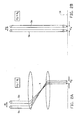
- FIGURES 2A and 2B The difference between these two approaches is shown in FIGURES 2A and 2B .
- FIGURE 2A an entire image comprising 2 electron beamlets 5a and 5b is demagnified to acquire the desired resolution.
- To demagnify an image requires at least one crossing X. In this crossing, all the electrons have to pass a small area. Coulomb interactions deteriorate the resolution at that crossing X.
- FIGURE 2B The method shown in FIGURE 2B may be used. Consider two adjacent beamlets 5a, 5b that are projected on the target exposure surface 14. Using the demagnification approach the distance between the two beamlets also becomes smaller. The focusing approach, however, does not change this distance between two beamlets. Only the cross section of each beamlet is reduced.
- the electron source 1 of FIGURE 1 typically delivers 100 A/cm 2 from an area of about 30-300 micron squared.
- a thermionic source is used.
- the electrons are preferably emitted in the space charge limited emission regime in order to benefit from a homogenizing effect of the space charge.
- Examples of such a source are a LaB 6 crystal, a dispenser source comprising Barium Oxide, or a dispenser source comprising a layer of Barium or Tungsten covered with Scandium Oxide.
- the extractor electrodes 2 usually, but not necessarily, focus the beam.
- the illumination lenses 3-4 create a parallel beam of electrons 5 on the aperture array 6.
- the lenses 3-4 are optimised to limit the beam energy spread as a result of Coulomb interactions, i.e. the opening angle of the beam is made as large as possible.
- lenses 3-4 are optimised to limit the beam blur created by chromatic and spherical aberration effects. For the latter it may be advantageous to use the aperture array 6 as a lens electrode, because this may create negative chromatic and spherical aberrations, resulting in a compensation of the aberrations of lenses 3-4.
- lens 4 for magnification of the pattern by slightly focusing or defocusing it.
- the electron beam emitted from the single emitter is focussed in a small crossover x before it is expanded.
- this crossover x there is a large energy spread due to electron-electron interactions in this crossover x.
- the crossover x will be imaged demagnified on the target exposure surface. Due to the Coulomb interactions the desired resolution is not achieved.
- a method to expand and collimate the expanded beam without a crossover is therefore desirable.
- crossover in the illumination electron optics is avoided by using an electron source 1 with a spherical or a hemispherical outer surface 15.
- a large opening angle ⁇ is formed, which reduces the blur due to electron-electron interactions in the emitted electron beam 5.
- the electron beams are forming a spherical wave front, which results in a virtual crossover 16 located in the centre of the source. There are no electrons present in the virtual crossover; so disturbing electron-electron interactions are absent.
- the electrons can be extracted with a spherical extractor that comprises large holes.
- the main advantage of the spherical shape of the extractor is the more homogeneous field that is created.
- crossover is avoided by extracting the electrons from the source/cathode 1 which is at a voltage Vs and has a distant planar extractor l1.
- the planar extractor has a positive voltage +V 1 with respect to the source 1.
- the combination of source and extractor now serves as a negative lens.
- the extracted electrons passing the extractor l 1 thus expand due to the diverging electric field. Again, a virtual crossover is created, which reduces the loss of resolution due to Coulomb interactions to a great extent.
- a space charged region S is present as is shown in FIGURE 3A . The presence of this space charge enhances the negative lens effect created by the source-extractor combination.
- V 1 By tuning V 1 it is possible to let the source 1 operate in its space charge limited emission mode.
- the main advantage of this emission mode is the significant increase of homogeneity of the emission.
- the increase of the total current can be limited by selecting a source with a confined emission area.
- the aperture array 6 has apertures of typically 5-150 ⁇ m in diameter with a pitch of about 50-500 ⁇ m.
- the apertures are preferably arranged in a hexagonal pattern.
- the aperture array 6 splits the incoming parallel beam of electrons 5 in a plurality of electron beamlets, typically in the order of about 5,000-30,000.
- the size of the apertures is adjusted to compensate non-uniform current density of the illumination.
- Each aperture has an area inversely proportional to the current density based on the individual beamlets that is transmitted through that same aperture. Consequently the current in each individual beamlet is the same. If the heat load on the aperture plate becomes too large, several aperture arrays are arranged in a serial order with decreasing aperture diameters along the path of the electron beam or plurality of electron beamlets. These aperture arrays have mutually aligned apertures.
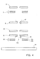
- FIGURE 4 shows a detail closer image of the lithography system in one of the embodiments starting from the plurality of beamlets.
- Condensor lens array 7 focuses each beamlet to a diameter of about 0,1-1 ⁇ m. It comprises two aligned plates with holes. The thickness of the plates is typically about 10-500 ⁇ m, while the holes are typically about 50-200 ⁇ m in diameter with a 50-500- ⁇ m pitch. Insulators (not shown), which are shielded from the beamlets, support the plates at typical distances of 1-10 millimetres from each other.
- the modulation array comprises a beamlet blanker array 8 and a beamlet stop array 10.
- the typical beam diameter is about 0,1-5 ⁇ m while the typical transversal energy is in the order of a 1-20 meV.
- Beamlet blanking means 17 are used to switch the electron beamlets on and off. They include blanking electrostatic deflectors, which comprise a number of electrodes. Preferably at least one electrode is grounded. Another electrode is connected to a circuit. Via this circuit control data are sent towards the blanking electrostatic deflectors. In this way, each blanking deflector can be controlled individually. Without the use of the beamlet blanking means 17 the electron beamlet will pass the beamlet stop array 10 through the apertures. When a voltage is applied on a blanking electrostatic deflector electrode in the beamlet blanker array 8, the corresponding electron beamlet will be deflected and terminate on the beamlet stop array 10.
- the beamlet blanker array 8 is located in the electrostatic focal plane of the electron beamlets. With the blanker array in this position, the system is less sensitive for distortions. In this embodiment, the beamlet stop array is positioned outside a focal plane of the electron beamlets.
- the transmitted beamlets now have to be focused on the target exposure surface 14.
- a focusing electron optical system 13 comprising at least one array with electrostatic lenses.
- Each individually transmitted electron beamlet is focused on the target exposure surface by a corresponding electrostatic lens.
- the lens array comprises two or more plates 13a and 13b, both having a thickness of about 10-500 ⁇ m and apertures 13c with a diameter of about 50-250 ⁇ m. The distance between two consecutive plates is somewhere between 50-800 ⁇ m and may be different from plate to plate.
- the focusing electron optical system may also comprise a lens array of the magnetic type. It is then located between the beamlet stop array 10 and the objective lens array of the electrostatic type 13, to further enhance the focusing properties of the electron optical system.
- a major problem in all electron beam lithography systems patterning a wafer or a mask is contamination. It reduces the performance of the lithography system significant due to the interaction between electrons and particles in the resist layer, the resist degrades. In a polymeric resist, molecules are released due to cracking. The released resist particles travel through the vacuum and can be absorbed by any of the structures present in the system.
- protective means are located in close proximity of the target exposure surface, i.e. between the target exposure surface and the focusing electron optical system.
- Said protective means may be a foil or a plate. Both options are provided with apertures with a diameter smaller than 20 ⁇ m.
- the protective means absorb the released resist particles before they can reach any of the sensitive elements in the lithography system. In some cases it is necessary to refresh the protective means after a predetermined period, e.g. after every processed wafer or mask. In the case of a protective plate the whole plate can be replaced.
- the foil is wound around the coil winders. A small section of the foil is tightened just above the entire target exposure surface 14. Only this section is exposed to the contaminants.
- the protective capacity of the foil rapidly degrades due to the absorbed particles.
- the exposed foil section then needs to be replaced. To do this the foil is transported from one coil winder to the other coil winder, thus exposing a fresh foil section to the contamination particles.
- an additional acceleration stage is positioned between the electrostatic lens array of the focusing electron optical system 13 and the protective means. This acceleration stage adds energy to the passing electrons.
- the beam may be accelerated additional tens of kiloelectronvolts, e.g. 50 keV.
- the beamlets 12 that have successfully passed the beamlet stop array 10 are directed towards the desired position on the target exposure surface 14 by two means.
- First of all actuation means move the target exposure surface 14 and the rest of the system in a certain mechanical scan direction relatively to each other.
- scan deflection means scan the transmitted beamlets 12 electrostatically in a direction that differs from the mechanical scan direction.
- the scan deflection means comprise electrostatic scan deflectors 18. In FIGURES 1 and 3 these scan deflectors 18 are located on an additional aperture array 11, and are depicted in figure 4 .
- the electrostatic scan deflectors 18 are deposited on the target exposure surface side of one of the plates of the objective electrostatic lens array 13, such that the deflection essentially occurs in the front focal plane of the objective lenses.
- the desired result is that the deflected beamlets impinge perpendicularly on the target surface.
- the combined deflection causes displacement of the beamlets a displacement of the beamlets at the target surface location, without changing the perpendicular axis of a beamlet with respect to the target surface.
- the electrostatic scan deflectors 18 are located on the protective means.
- the electrostatic scan deflectors 18 comprise scan deflection electrodes, which are arranged to deflect an assembly of electron beamlets in the same direction.
- the scan deflection electrodes may be deposited in the form of strips 19 on a suitable plate 20 at the target exposure surface side as is shown in FIGURE 5A .
- the best yield can be established when the strips 19 are deposited close to the beamlet, thus close to the aperture 21, since this reduces d b-sd .
- the first assembly is scanned in one direction while the next one is scanned in the opposite direction, by putting alternating voltages on the consecutive strips 19 as is shown in FIGURE 5B .
- the first strip has for instance a positive potential, the second one a negative potential, the next one a positive etc.
- the scan direction is denoted y .
- One line of transmitted electron beamlets is then scanned in the - y -direction, while at the same time the next line is directed towards + y .
- the mechanical scan can be performed in three ways.
- the target exposure surface moves, the rest of the system moves or they both move in different directions.
- the deflection scan is performed in a different direction compared to the mechanical scan. It is preferably perpendicular or almost perpendicular to the mechanical scan direction, because the scan deflection length ⁇ x is then larger for the same deflection scan angle ⁇ sd .
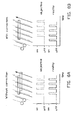
- the first one is a triangular shaped scan trajectory ( FIGURE 6A )
- the second one a saw tooth shaped scan trajectory ( FIGURE 6B ).
- an assembly of electron beam exposure apparatuses as described above is used to expose the entire wafer at the same time.
- the writing strategy described above is based on the assumption that the beamlet can only be switched on or off. To reduce the amount of data by less grid lines, and thus less grid cells seems a logical approach. However, the dimension control of the desired pattern suffers considerably.
- An approach to circumvent this problem is to pattern the target exposure surface 14 with discrete dose control. Again the pattern is divided according to a rectangular grid. However, the number of grid lines is much smaller e.g. 2-5 per dimension, which results in a number of grid points of about 4-25.
- the intensity of each grid cell is variable. The intensity is represented by a so-called gray value.
- the values are 0, 1/7, 2/7, 3/7, 4/7, 5/7, 6/7 and 1 times the maximum dose.
- the number of data required for the position of the beamlet reduces, although each cell is represented with more information due to the controlled dose variation.
- Gray scale writing can be introduced in several ways.
- First of all the deflection of the beams may be controlled in such a way that part of the beam passes the beamlet stop array 10, while part of the beam continues traveling towards the target exposure surface 14.
- 1/3 or 2/3 of the beam can be stopped, resulting in 4 possible doses on the target exposure surface, namely 0, 1/3, 2/3 and 1 times the maximum dose, corresponding to a 2 bit gray value representation.
- Another method to create gray levels is to deflect the beamlets in such a way that they do not move with respect to the target surface for a predetermined amount of time T, which amount of time T is longer than a minimum on/off time of the blankers. During time T, the modulator can now deposite 1, 2, 3, etc. shots on one position, thus creating gray levels.
- Another method to create these 4 so-called gray values is to change the aperture size in the aperture array 6. If there are for instance three aperture sizes, the original size, a size that permits half the original current to pass and apertures with an area such that only a fourth of the original current passes, the same discrete dose values as mentioned before an be created. By switching the beamlets on and off with the deflection electrodes 17 of the beamlet blanker array 8 the desired dose can be deposited on the target exposure surface 14.
- a disadvantage of the latter method is the fact that more beamlets are needed to write one pixel.
- Most, including aforementioned methods for discrete dose control can also be used to create more than 4 gray values, e.g. 8, 16, 32 or 64.
- the positions of the beamlets on the target exposure surface most often do not exactly correspond with the desired positions. This is for instance due to misalignment of the different arrays with respect to each other. Additionally, manufacturing errors may also contribute to the offset of the individual beamlets.
- To transfer the correct pattern from the controller onto the exposure surface of the target corrections have to be made. To this end, in a particular embodiment, first the position of all beamlets is measured and stored. Each position is then compared to the position the beamlet should have. The difference in position is then integrated in the pattern information that is sent to the modulation means.
- FIGURES 7A-7D and 8A-8B explain how the adjustments are implemented.
- the beamlet scan is performed by combining two scan mechanisms: a mechanical scan and a deflection scan. All pattern data, which is sent to each beamlet, is supplied per deflection scan line.
- the desired deflection scan width on the exposure surface of the target that is patterned, W scan is smaller than the deflection scan width the apparatus can handle, W overscan , as is shown in FIGURES 7A AND 7B.
- the overscan ability enables a correction in the deflection scan direction.
- the beamlet In figure 7A the beamlet is positioned correctly. In figure 7B , however, the beamlet has shifted to the right.
- the timing By adjusting the timing in such a way that the pattern data is applied when the beamlet enters the desired area, the offset can be compensated for.
- the adjustment in the mechanical scan direction is less precise than depicted in FIGURE 7B . Since the pattern data is written per scan line, only a discrete time delay is possible, i.e. pattern generation can be postponed or accelerated per scan line. A random time delay would result in a completely new control data sequence. A calculation of such a new sequence takes a lot of time and is therefore not desirable.
- FIGURES 7C AND 7D is depicted what the consequence is.
- the desired location of the beamlet is shown together with its first five corresponding scan lines.
- the real position of the beamlet and its trajectories is shown.
- the desired beamlet and scan lines are also depicted with an empty circle and dashed lines, respectively. It can be seen that the first scan line in the desired situation does not cover the area that needs to be patterned by the beamlet. So the beamlet start patterning halfway the second scan line. Effectively the delay of information has taken a time period that is necessary to scan one deflection scan line.
- FIGURES 8A and 8B show an example of how a change in the timing corrects for the initial incorrect position of a structure written by a not ideally positioned beamlet.
- FIGURE 8A depicts the situation without any timing correction.
- the empty dot represents the beamlet at the correct position, while the filled one represents the real location of the beamlet.
- the beamlet is scanned along the drawn line to write a pattern.
- the line is dashed in the ideal case and solid in the real case.
- the written structure is a single line.
- FIGURE 8B shows the situation wherein timing correction is applied. Again the theoretical and actual spots and trajectories are depicted with dashed and solid lines and dots respectively.
- the signal sequence in the real situation is different than the theoretical pattern information, in the fact that the signal sequence in the real situation (lower curve) is sent at a different time than the same sequence is sent in the idea configuration (upper curve).
- the single line is now written at the correct location in the deflection scan direction.
- the pattern processing started one scan line earlier resulting in a better positioning of the single line in the mechanical scan direction as well. Note that the single line is not precisely positioned at the correct location. This is due to the slight offset between the scan lines in the ideal and the real situation.
- the current electron beam exposure system is thus capable of dynamically adjusting the position of a scanned line using timing corrections.
- This allows for critical components in a pattern to be written in one scan line instead of using two halves of two scan lines, which would spread the critical component over two scan lines.
- This correction can also be done locally, i.e. the timing can be corrected over a small time window.
- the controller should thus identify critical components, which would normally be spread over two scan lines. Subsequently, the controller should calculated a corrected timing window, and apply the corrected timing window to the timing base used for scanning an electron beamlet.
- Figure 7D shows the adjustment principle, which could be used for this.
- All lens plates, aperture plates and blanker plates can be connected to a power supply, which, when gas is admitted into the system, creates a plasma.
- the plasma cleans the plates and removes all contamination. If one plasma does not clean thorough enough, two gases may be admitted into the system in series. For instance oxygen may be admitted first to remove all hydrocarbons residing in the system. After the removal of the oxygen plasma, a second plasma, for instance comprising HF, is created to remove all present oxides.
- Another possibility to reduce the contamination is to perform all operations at elevated temperatures, i.e. 150-400 °C.
- a pretreatment at 1000-1500 °C may be necessary. At these temperatures hydrocarbons get no chance to condense on any of the elements in the system. Allowing a fraction of oxygen into the system can further enhance the cleaning process.
Landscapes
- Chemical & Material Sciences (AREA)
- Engineering & Computer Science (AREA)
- Analytical Chemistry (AREA)
- Nanotechnology (AREA)
- Crystallography & Structural Chemistry (AREA)
- Physics & Mathematics (AREA)
- General Physics & Mathematics (AREA)
- Manufacturing & Machinery (AREA)
- Condensed Matter Physics & Semiconductors (AREA)
- Mathematical Physics (AREA)
- Theoretical Computer Science (AREA)
- Electron Beam Exposure (AREA)
- X-Ray Techniques (AREA)
Applications Claiming Priority (2)
| Application Number | Priority Date | Filing Date | Title |
|---|---|---|---|
| US42275802P | 2002-10-30 | 2002-10-30 | |
| EP03809889.3A EP1556881B1 (de) | 2002-10-30 | 2003-10-30 | Elektronenstrahlbelichtungssystem |
Related Parent Applications (2)
| Application Number | Title | Priority Date | Filing Date |
|---|---|---|---|
| EP03809889.3 Division | 2003-10-30 | ||
| EP03809889.3A Division EP1556881B1 (de) | 2002-10-30 | 2003-10-30 | Elektronenstrahlbelichtungssystem |
Publications (2)
| Publication Number | Publication Date |
|---|---|
| EP2565902A2 true EP2565902A2 (de) | 2013-03-06 |
| EP2565902A3 EP2565902A3 (de) | 2017-07-05 |
Family
ID=32230384
Family Applications (5)
| Application Number | Title | Priority Date | Filing Date |
|---|---|---|---|
| EP03809889.3A Expired - Lifetime EP1556881B1 (de) | 2002-10-30 | 2003-10-30 | Elektronenstrahlbelichtungssystem |
| EP12188366.4A Withdrawn EP2565902A3 (de) | 2002-10-30 | 2003-10-30 | Elektronenstrahl-Belichtungssystem |
| EP13179104.8A Expired - Lifetime EP2701178B1 (de) | 2002-10-30 | 2003-10-30 | Elektronenstrahlbelichtungssystem |
| EP20150683.9A Withdrawn EP3671804A1 (de) | 2002-10-30 | 2003-10-30 | Elektronenstrahlbelichtungssystem |
| EP12179910.0A Withdrawn EP2523207A3 (de) | 2002-10-30 | 2003-10-30 | Elektronenstrahlgenerator |
Family Applications Before (1)
| Application Number | Title | Priority Date | Filing Date |
|---|---|---|---|
| EP03809889.3A Expired - Lifetime EP1556881B1 (de) | 2002-10-30 | 2003-10-30 | Elektronenstrahlbelichtungssystem |
Family Applications After (3)
| Application Number | Title | Priority Date | Filing Date |
|---|---|---|---|
| EP13179104.8A Expired - Lifetime EP2701178B1 (de) | 2002-10-30 | 2003-10-30 | Elektronenstrahlbelichtungssystem |
| EP20150683.9A Withdrawn EP3671804A1 (de) | 2002-10-30 | 2003-10-30 | Elektronenstrahlbelichtungssystem |
| EP12179910.0A Withdrawn EP2523207A3 (de) | 2002-10-30 | 2003-10-30 | Elektronenstrahlgenerator |
Country Status (7)
| Country | Link |
|---|---|
| US (5) | US6897458B2 (de) |
| EP (5) | EP1556881B1 (de) |
| JP (2) | JP5053514B2 (de) |
| KR (5) | KR101077098B1 (de) |
| CN (11) | CN101414129B (de) |
| AU (1) | AU2003276779A1 (de) |
| WO (1) | WO2004040614A2 (de) |
Families Citing this family (148)
| Publication number | Priority date | Publication date | Assignee | Title |
|---|---|---|---|---|
| CN101414129B (zh) * | 2002-10-30 | 2012-11-28 | 迈普尔平版印刷Ip有限公司 | 电子束曝光系统 |
| EP1515359A1 (de) * | 2003-09-12 | 2005-03-16 | ICT Integrated Circuit Testing Gesellschaft für Halbleiterprüftechnik mbH | Kammer mit geringer durch Elektronen stimulierter Desorption |
| KR101099487B1 (ko) * | 2004-05-17 | 2011-12-28 | 마퍼 리쏘그라피 아이피 비.브이. | 대전 입자 빔 노광 시스템 |
| US7425713B2 (en) * | 2005-01-14 | 2008-09-16 | Arradiance, Inc. | Synchronous raster scanning lithographic system |
| JP5154232B2 (ja) * | 2005-02-18 | 2013-02-27 | アイエムエス ナノファブリケーション エージー | 荷電粒子暴露装置 |
| JP4708854B2 (ja) * | 2005-05-13 | 2011-06-22 | 株式会社日立ハイテクノロジーズ | 荷電粒子線装置 |
| JP5222142B2 (ja) * | 2005-09-06 | 2013-06-26 | カール・ツァイス・エスエムティー・ゲーエムベーハー | 粒子光学部品 |
| WO2007032671A1 (en) * | 2005-09-16 | 2007-03-22 | Mapper Lithography Ip B.V. | Lithography system and projection method |
| US7883839B2 (en) * | 2005-12-08 | 2011-02-08 | University Of Houston | Method and apparatus for nano-pantography |
| US7569834B1 (en) | 2006-10-18 | 2009-08-04 | Kla-Tencor Technologies Corporation | High resolution charged particle projection lens array using magnetic elements |
| EP2019415B1 (de) * | 2007-07-24 | 2016-05-11 | IMS Nanofabrication AG | Mehrfachstrahlquelle |
| US8445869B2 (en) | 2008-04-15 | 2013-05-21 | Mapper Lithography Ip B.V. | Projection lens arrangement |
| EP2260499B1 (de) * | 2008-02-26 | 2016-11-30 | Mapper Lithography IP B.V. | Projektionslinsenanordnung |
| KR101481950B1 (ko) * | 2008-02-26 | 2015-01-14 | 마퍼 리쏘그라피 아이피 비.브이. | 투사 렌즈 배열체 |
| US8890094B2 (en) | 2008-02-26 | 2014-11-18 | Mapper Lithography Ip B.V. | Projection lens arrangement |
| JP5203992B2 (ja) * | 2008-03-25 | 2013-06-05 | 株式会社ニューフレアテクノロジー | 電子ビーム描画装置及び電子ビーム描画方法 |
| CN102067271B (zh) | 2008-04-15 | 2014-05-21 | 迈普尔平版印刷Ip有限公司 | 子束阻断器装置 |
| US7851774B2 (en) * | 2008-04-25 | 2010-12-14 | Taiwan Semiconductor Manufacturing Company, Ltd. | System and method for direct writing to a wafer |
| US8502176B2 (en) * | 2008-05-23 | 2013-08-06 | Mapper Lithography Ip B.V. | Imaging system |
| WO2009147202A1 (en) | 2008-06-04 | 2009-12-10 | Mapper Lithography Ip B.V. | Writing strategy |
| NL2003304C2 (en) * | 2008-08-07 | 2010-09-14 | Ims Nanofabrication Ag | Compensation of dose inhomogeneity and image distortion. |
| US8796644B2 (en) | 2008-08-18 | 2014-08-05 | Mapper Lithography Ip B.V. | Charged particle beam lithography system and target positioning device |
| TWI472884B (zh) * | 2008-08-18 | 2015-02-11 | Mapper Lithography Ip Bv | 帶電粒子射束微影系統以及目標物定位裝置 |
| US9323140B2 (en) | 2008-09-01 | 2016-04-26 | D2S, Inc. | Method and system for forming a pattern on a reticle using charged particle beam lithography |
| US20120219886A1 (en) | 2011-02-28 | 2012-08-30 | D2S, Inc. | Method and system for forming patterns using charged particle beam lithography with variable pattern dosage |
| US9341936B2 (en) | 2008-09-01 | 2016-05-17 | D2S, Inc. | Method and system for forming a pattern on a reticle using charged particle beam lithography |
| US8057970B2 (en) | 2008-09-01 | 2011-11-15 | D2S, Inc. | Method and system for forming circular patterns on a surface |
| US20140353526A1 (en) * | 2008-09-01 | 2014-12-04 | D2S, Inc. | Method and system for forming high accuracy patterns using charged particle beam lithography |
| US8473875B2 (en) | 2010-10-13 | 2013-06-25 | D2S, Inc. | Method and system for forming high accuracy patterns using charged particle beam lithography |
| US7901850B2 (en) | 2008-09-01 | 2011-03-08 | D2S, Inc. | Method and system for design of a reticle to be manufactured using variable shaped beam lithography |
| US8670106B2 (en) | 2008-09-23 | 2014-03-11 | Pinebrook Imaging, Inc. | Optical imaging writer system |
| US8395752B2 (en) | 2008-09-23 | 2013-03-12 | Pinebrook Imaging Technology, Ltd. | Optical imaging writer system |
| US8390781B2 (en) | 2008-09-23 | 2013-03-05 | Pinebrook Imaging Technology, Ltd. | Optical imaging writer system |
| US8253923B1 (en) | 2008-09-23 | 2012-08-28 | Pinebrook Imaging Technology, Ltd. | Optical imaging writer system |
| US8390786B2 (en) | 2008-09-23 | 2013-03-05 | Pinebrook Imaging Technology, Ltd. | Optical imaging writer system |
| DE102008049655A1 (de) | 2008-09-30 | 2010-04-08 | Carl Zeiss Nts Gmbh | Partikelstrahlsystem und Verfahren zum Betreiben desselben |
| US8366423B2 (en) | 2009-02-22 | 2013-02-05 | Mapper Lithography Ip B.V. | Method and arrangement for realizing a vacuum in a vacuum chamber |
| CN102422380A (zh) | 2009-02-22 | 2012-04-18 | 迈普尔平版印刷Ip有限公司 | 带电粒子微影设备及真空腔室中产生真空的方法 |
| JP5762981B2 (ja) | 2009-02-22 | 2015-08-12 | マッパー・リソグラフィー・アイピー・ビー.ブイ. | 荷電粒子リソグラフィ装置と、真空チャンバー内の真空を生成する方法 |
| WO2010094804A1 (en) | 2009-02-22 | 2010-08-26 | Mapper Lithography Ip B.V. | Lithography machine and substrate handling arrangement |
| WO2010100270A1 (en) * | 2009-03-06 | 2010-09-10 | Micronic Laser Systems Ab | Method and apparatus for statistical illumination |
| TWI497557B (zh) * | 2009-04-29 | 2015-08-21 | Mapper Lithography Ip Bv | 包含靜電偏轉器的帶電粒子光學系統 |
| EP3144955A1 (de) | 2009-05-20 | 2017-03-22 | Mapper Lithography IP B.V. | Verfahren zum belichten eines wafers |
| CN102460633B (zh) | 2009-05-20 | 2014-12-17 | 迈普尔平版印刷Ip有限公司 | 用于光刻系统的图案数据转换器 |
| WO2010134017A1 (en) | 2009-05-20 | 2010-11-25 | Mapper Lithography Ip B.V. | Method of generating a two-level pattern for lithographic processing and pattern generator using the same |
| US9448473B2 (en) | 2009-08-26 | 2016-09-20 | D2S, Inc. | Method for fracturing and forming a pattern using shaped beam charged particle beam lithography |
| US9164372B2 (en) | 2009-08-26 | 2015-10-20 | D2S, Inc. | Method and system for forming non-manhattan patterns using variable shaped beam lithography |
| NL2003619C2 (en) | 2009-10-09 | 2011-04-12 | Mapper Lithography Ip Bv | Projection lens assembly. |
| US8987679B2 (en) * | 2009-10-09 | 2015-03-24 | Mapper Lithography Ip B.V. | Enhanced integrity projection lens assembly |
| US8987677B2 (en) * | 2009-10-26 | 2015-03-24 | Mapper Lithography Ip B.V. | Charged particle multi-beamlet lithography system, modulation device, and method of manufacturing thereof |
| US8952342B2 (en) | 2009-12-17 | 2015-02-10 | Mapper Lithography Ip B.V. | Support and positioning structure, semiconductor equipment system and method for positioning |
| NL1037639C2 (en) | 2010-01-21 | 2011-07-25 | Mapper Lithography Ip Bv | Lithography system with lens rotation. |
| JP5988537B2 (ja) * | 2010-06-10 | 2016-09-07 | 株式会社ニコン | 荷電粒子線露光装置及びデバイス製造方法 |
| TWI534852B (zh) | 2010-10-26 | 2016-05-21 | 瑪波微影Ip公司 | 微影系統、調整裝置及製造光纖固定基板之方法 |
| TWI562186B (en) | 2010-11-13 | 2016-12-11 | Mapper Lithography Ip Bv | Charged particle lithography system and method for transferring a pattern onto a surface of a target and modulation device for use in a charged particle lithography system |
| TWI517196B (zh) | 2010-11-13 | 2016-01-11 | 瑪波微影Ip公司 | 具有中間腔室的帶電粒子微影系統 |
| TWI562183B (en) | 2010-11-13 | 2016-12-11 | Mapper Lithography Ip Bv | Aperture array element, charged particle beam generator and charged particle lithography system |
| US9305747B2 (en) | 2010-11-13 | 2016-04-05 | Mapper Lithography Ip B.V. | Data path for lithography apparatus |
| US8884255B2 (en) | 2010-11-13 | 2014-11-11 | Mapper Lithography Ip B.V. | Data path for lithography apparatus |
| RU2579533C2 (ru) | 2010-12-14 | 2016-04-10 | МЭППЕР ЛИТОГРАФИ АйПи Б. В. | Литографическая система и способ обработки подложек в такой литографической системе |
| EP2673243B1 (de) | 2011-02-07 | 2021-07-07 | Nederlandse Organisatie voor toegepast- natuurwetenschappelijk onderzoek TNO | Chemischer kohlenstoffdioxidgasgenerator |
| JP5902201B2 (ja) | 2011-02-16 | 2016-04-13 | マッパー・リソグラフィー・アイピー・ビー.ブイ. | 磁気シールド用システム |
| US9612530B2 (en) | 2011-02-28 | 2017-04-04 | D2S, Inc. | Method and system for design of enhanced edge slope patterns for charged particle beam lithography |
| US9057956B2 (en) | 2011-02-28 | 2015-06-16 | D2S, Inc. | Method and system for design of enhanced edge slope patterns for charged particle beam lithography |
| US8362425B2 (en) * | 2011-03-23 | 2013-01-29 | Kla-Tencor Corporation | Multiple-beam system for high-speed electron-beam inspection |
| KR102072200B1 (ko) | 2011-04-22 | 2020-01-31 | 에이에스엠엘 네델란즈 비.브이. | 리소그래피 머신들의 클러스터를 위한 네트워크 아키텍처 및 프로토콜 |
| NL2007604C2 (en) * | 2011-10-14 | 2013-05-01 | Mapper Lithography Ip Bv | Charged particle system comprising a manipulator device for manipulation of one or more charged particle beams. |
| US8936994B2 (en) | 2011-04-28 | 2015-01-20 | Mapper Lithography Ip B.V. | Method of processing a substrate in a lithography system |
| US9328512B2 (en) | 2011-05-05 | 2016-05-03 | Eversealed Windows, Inc. | Method and apparatus for an insulating glazing unit and compliant seal for an insulating glazing unit |
| JP5905209B2 (ja) * | 2011-05-18 | 2016-04-20 | 株式会社ニューフレアテクノロジー | 荷電粒子ビーム描画装置および荷電粒子ビーム描画方法 |
| NL2006868C2 (en) * | 2011-05-30 | 2012-12-03 | Mapper Lithography Ip Bv | Charged particle multi-beamlet apparatus. |
| US9034542B2 (en) | 2011-06-25 | 2015-05-19 | D2S, Inc. | Method and system for forming patterns with charged particle beam lithography |
| US8698094B1 (en) * | 2011-07-20 | 2014-04-15 | Kla-Tencor Corporation | Permanent magnet lens array |
| CN103959919A (zh) * | 2011-09-28 | 2014-07-30 | 迈普尔平版印刷Ip有限公司 | 等离子产生器 |
| USRE49732E1 (en) | 2012-03-08 | 2023-11-21 | Asml Netherlands B.V. | Charged particle lithography system with alignment sensor and beam measurement sensor |
| JP6239583B2 (ja) * | 2012-03-20 | 2017-11-29 | マッパー・リソグラフィー・アイピー・ビー.ブイ. | ラジカルを輸送するための装置および方法 |
| JP6128744B2 (ja) * | 2012-04-04 | 2017-05-17 | キヤノン株式会社 | 描画装置、描画方法、および、物品の製造方法 |
| KR20150001834A (ko) | 2012-04-18 | 2015-01-06 | 디2에스, 인코포레이티드 | 하전 입자 빔 리소그래피를 사용한 임계 치수 균일성을 위한 방법 및 시스템 |
| WO2013158573A1 (en) | 2012-04-18 | 2013-10-24 | D2S, Inc. | Method and system for forming patterns using charged particle beam lithograph |
| US9343267B2 (en) | 2012-04-18 | 2016-05-17 | D2S, Inc. | Method and system for dimensional uniformity using charged particle beam lithography |
| WO2013171229A1 (en) | 2012-05-14 | 2013-11-21 | Mapper Lithography Ip B.V. | Charged particle lithography system and beam generator |
| US10586625B2 (en) | 2012-05-14 | 2020-03-10 | Asml Netherlands B.V. | Vacuum chamber arrangement for charged particle beam generator |
| NL2010759C2 (en) | 2012-05-14 | 2015-08-25 | Mapper Lithography Ip Bv | Modulation device and power supply arrangement. |
| US11348756B2 (en) | 2012-05-14 | 2022-05-31 | Asml Netherlands B.V. | Aberration correction in charged particle system |
| NL2010799C2 (en) | 2012-05-14 | 2014-02-03 | Mapper Lithography Ip Bv | Charged particle multi-beamlet lithography system and cooling arrangement manufacturing method. |
| NL2010760C2 (en) | 2013-05-03 | 2014-11-04 | Mapper Lithography Ip Bv | Beam grid layout. |
| JP6212299B2 (ja) * | 2013-06-26 | 2017-10-11 | キヤノン株式会社 | ブランキング装置、描画装置、および物品の製造方法 |
| WO2015024956A1 (en) | 2013-08-23 | 2015-02-26 | Mapper Lithography Ip B.V. | Drying device for use in a lithography system |
| RU2644388C2 (ru) * | 2013-11-14 | 2018-02-12 | МЭППЕР ЛИТОГРАФИ АйПи Б.В. | Многоэлектродная охлаждаемая конструкция |
| US8975601B1 (en) * | 2013-11-25 | 2015-03-10 | Taiwan Semiconductor Manufacturing Company, Ltd. | Method and apparatus for electron beam lithography |
| NL2014030B1 (en) * | 2013-12-30 | 2016-01-08 | Mapper Lithography Ip Bv | Cathode arrangement, electron gun, and lithograpy system comprising such electron gun. |
| US9460260B2 (en) | 2014-02-21 | 2016-10-04 | Mapper Lithography Ip B.V. | Enhanced stitching by overlap dose and feature reduction |
| US9514912B2 (en) * | 2014-09-10 | 2016-12-06 | Varian Semiconductor Equipment Associates, Inc. | Control of ion angular distribution of ion beams with hidden deflection electrode |
| KR20170084240A (ko) | 2014-11-14 | 2017-07-19 | 마퍼 리쏘그라피 아이피 비.브이. | 리소그래피 시스템에서 기판을 이송하기 위한 로드 로크 시스템 및 방법 |
| DE102015202172B4 (de) | 2015-02-06 | 2017-01-19 | Carl Zeiss Microscopy Gmbh | Teilchenstrahlsystem und Verfahren zur teilchenoptischen Untersuchung eines Objekts |
| US9691588B2 (en) | 2015-03-10 | 2017-06-27 | Hermes Microvision, Inc. | Apparatus of plural charged-particle beams |
| US9484188B2 (en) | 2015-03-11 | 2016-11-01 | Mapper Lithography Ip B.V. | Individual beam pattern placement verification in multiple beam lithography |
| TWI722855B (zh) | 2015-03-24 | 2021-03-21 | 美商克萊譚克公司 | 用於具有改良之影像光束穩定性及詢問之帶電粒子顯微鏡之方法及系統 |
| US10096450B2 (en) * | 2015-12-28 | 2018-10-09 | Mapper Lithography Ip B.V. | Control system and method for lithography apparatus |
| JP6550478B2 (ja) * | 2016-04-13 | 2019-07-24 | エーエスエムエル ネザーランズ ビー.ブイ. | マルチビーム装置、荷電粒子ビーム装置、ソース変換ユニット、ソース変換ユニットを構成する方法、仮想的マルチソースアレイを形成するための方法 |
| US9981293B2 (en) | 2016-04-21 | 2018-05-29 | Mapper Lithography Ip B.V. | Method and system for the removal and/or avoidance of contamination in charged particle beam systems |
| CN106019854A (zh) * | 2016-07-18 | 2016-10-12 | 无锡宏纳科技有限公司 | 图形可变的电子束光刻机 |
| JP2018098268A (ja) * | 2016-12-08 | 2018-06-21 | 株式会社ニューフレアテクノロジー | ブランキング偏向器及びマルチ荷電粒子ビーム描画装置 |
| CN110268330B (zh) * | 2016-12-23 | 2022-01-28 | Asml荷兰有限公司 | 一种使用无掩模光刻曝光系统制造电子器件的方法和系统 |
| TWI742223B (zh) * | 2017-01-14 | 2021-10-11 | 美商克萊譚克公司 | 電子束系統及方法,以及掃描電子顯微鏡 |
| US10242839B2 (en) * | 2017-05-05 | 2019-03-26 | Kla-Tencor Corporation | Reduced Coulomb interactions in a multi-beam column |
| KR102634195B1 (ko) | 2017-09-29 | 2024-02-07 | 에이에스엠엘 네델란즈 비.브이. | 하전 입자의 빔 조건을 조정하기 위한 방법 및 장치 |
| JP2019114748A (ja) * | 2017-12-26 | 2019-07-11 | 株式会社ニューフレアテクノロジー | マルチ荷電粒子ビーム描画方法及びマルチ荷電粒子ビーム描画装置 |
| DE102018202421B3 (de) | 2018-02-16 | 2019-07-11 | Carl Zeiss Microscopy Gmbh | Vielstrahl-Teilchenstrahlsystem |
| DE102018202428B3 (de) | 2018-02-16 | 2019-05-09 | Carl Zeiss Microscopy Gmbh | Vielstrahl-Teilchenmikroskop |
| CN112055886A (zh) | 2018-02-27 | 2020-12-08 | 卡尔蔡司MultiSEM有限责任公司 | 带电粒子多束系统及方法 |
| US10438769B1 (en) * | 2018-05-02 | 2019-10-08 | Kla-Tencor Corporation | Array-based characterization tool |
| US10811215B2 (en) | 2018-05-21 | 2020-10-20 | Carl Zeiss Multisem Gmbh | Charged particle beam system |
| DE102018115012A1 (de) | 2018-06-21 | 2019-12-24 | Carl Zeiss Microscopy Gmbh | Teilchenstrahlsystem |
| US10483080B1 (en) * | 2018-07-17 | 2019-11-19 | ICT Integrated Circuit Testing Gesellschaft für Halbleiterprüftechnik mbH | Charged particle beam device, multi-beam blanker for a charged particle beam device, and method for operating a charged particle beam device |
| US10593509B2 (en) | 2018-07-17 | 2020-03-17 | ICT Integrated Circuit Testing Gesellschaft für Halbleiterprüftechnik mbH | Charged particle beam device, multi-beam blanker for a charged particle beam device, and method for operating a charged particle beam device |
| DE102018007455B4 (de) | 2018-09-21 | 2020-07-09 | Carl Zeiss Multisem Gmbh | Verfahren zum Detektorabgleich bei der Abbildung von Objekten mittels eines Mehrstrahl-Teilchenmikroskops, System sowie Computerprogrammprodukt |
| DE102018007652B4 (de) | 2018-09-27 | 2021-03-25 | Carl Zeiss Multisem Gmbh | Teilchenstrahl-System sowie Verfahren zur Stromregulierung von Einzel-Teilchenstrahlen |
| DE102018124044B3 (de) | 2018-09-28 | 2020-02-06 | Carl Zeiss Microscopy Gmbh | Verfahren zum Betreiben eines Vielstrahl-Teilchenstrahlmikroskops und Vielstrahl-Teilchenstrahlsystem |
| DE102018124219A1 (de) | 2018-10-01 | 2020-04-02 | Carl Zeiss Microscopy Gmbh | Vielstrahl-Teilchenstrahlsystem und Verfahren zum Betreiben eines solchen |
| NL2022156B1 (en) | 2018-12-10 | 2020-07-02 | Asml Netherlands Bv | Plasma source control circuit |
| CN113272934B (zh) * | 2018-12-28 | 2024-11-29 | Asml荷兰有限公司 | 用于多个带电粒子束的装置 |
| TWI743626B (zh) | 2019-01-24 | 2021-10-21 | 德商卡爾蔡司多重掃描電子顯微鏡有限公司 | 包含多束粒子顯微鏡的系統、對3d樣本逐層成像之方法及電腦程式產品 |
| CN111477530B (zh) | 2019-01-24 | 2023-05-05 | 卡尔蔡司MultiSEM有限责任公司 | 利用多束粒子显微镜对3d样本成像的方法 |
| DE102019004124B4 (de) | 2019-06-13 | 2024-03-21 | Carl Zeiss Multisem Gmbh | Teilchenstrahl-System zur azimutalen Ablenkung von Einzel-Teilchenstrahlen sowie seine Verwendung und Verfahren zur Azimut-Korrektur bei einem Teilchenstrahl-System |
| DE102019005362A1 (de) | 2019-07-31 | 2021-02-04 | Carl Zeiss Multisem Gmbh | Verfahren zum Betreiben eines Vielzahl-Teilchenstrahlsystems unter Veränderung der numerischen Apertur, zugehöriges Computerprogrammprodukt und Vielzahl-Teilchenstrahlsystem |
| DE102019008249B3 (de) | 2019-11-27 | 2020-11-19 | Carl Zeiss Multisem Gmbh | Teilchenstrahl-System mit einer Multistrahl-Ablenkeinrichtung und einem Strahlfänger, Verfahren zum Betreiben des Teilchenstrahl-Systems und zugehöriges Computerprogrammprodukt |
| WO2021156198A1 (en) | 2020-02-04 | 2021-08-12 | Carl Zeiss Multisem Gmbh | Multi-beam digital scan and image acquisition |
| EP3863040A1 (de) * | 2020-02-07 | 2021-08-11 | ASML Netherlands B.V. | Manipulatorvorrichtung für geladene partikel |
| EP4734148A2 (de) | 2020-03-12 | 2026-04-29 | Carl Zeiss MultiSEM GmbH | Bestimmte verbesserungen von mehrstrahlerzeugungs- und mehrstrahlablenkeinheiten |
| DE102020107738B3 (de) | 2020-03-20 | 2021-01-14 | Carl Zeiss Multisem Gmbh | Teilchenstrahl-System mit einer Multipol-Linsen-Sequenz zur unabhängigen Fokussierung einer Vielzahl von Einzel-Teilchenstrahlen, seine Verwendung und zugehöriges Verfahren |
| US10937630B1 (en) | 2020-04-27 | 2021-03-02 | John Bennett | Modular parallel electron lithography |
| US12525426B2 (en) | 2020-05-01 | 2026-01-13 | Asml Netherlands B.V. | Enhanced architecture for high-performance detection device |
| CN115917700B (zh) | 2020-05-28 | 2026-04-24 | Asml荷兰有限公司 | 用于高性能检测设备技术领域的增强架构 |
| EP3928833A1 (de) * | 2020-06-24 | 2021-12-29 | Centre Hospitalier Universitaire Vaudois (CHUV) | Vorrichtung zur bereitstellung einer strahlungsbehandlung |
| DE102020123567B4 (de) | 2020-09-09 | 2025-02-13 | Carl Zeiss Multisem Gmbh | Vielzahl-Teilchenstrahl-System mit Kontrast-Korrektur-Linsen-System |
| TW202220012A (zh) | 2020-09-30 | 2022-05-16 | 德商卡爾蔡司多重掃描電子顯微鏡有限公司 | 在可調工作距離附近具快速自動對焦之多重粒子束顯微鏡及相關方法 |
| DE102021200799B3 (de) | 2021-01-29 | 2022-03-31 | Carl Zeiss Multisem Gmbh | Verfahren mit verbesserter Fokuseinstellung unter Berücksichtigung eines Bildebenenkipps in einem Vielzahl-Teilchenstrahlmikroskop |
| CA3215592A1 (en) | 2021-04-16 | 2022-10-20 | Ruth Shewmon Bloom | Arbitrary electron dose waveforms for electron microscopy |
| TW202312205A (zh) | 2021-05-27 | 2023-03-16 | 德商卡爾蔡司多重掃描電子顯微鏡有限公司 | 多重射束帶電粒子系統與在多重射束帶電粒子系統中控制工作距離的方法 |
| JP7795055B2 (ja) | 2021-06-16 | 2026-01-07 | カール ツァイス マルティセム ゲゼルシヤフト ミット ベシュレンクテル ハフツング | 歪み最適化マルチビーム走査システム |
| DE102021116969B3 (de) | 2021-07-01 | 2022-09-22 | Carl Zeiss Multisem Gmbh | Verfahren zur bereichsweisen Probeninspektion mittels eines Vielstrahl-Teilchenmikroskopes, Computerprogrammprodukt und Vielstrahl-Teilchenmikroskop zur Halbleiterprobeninspektion |
| US12057287B2 (en) * | 2022-03-30 | 2024-08-06 | Fei Company | Methods and systems for aligning a multi-beam system |
| JP2023150799A (ja) * | 2022-03-31 | 2023-10-16 | 株式会社日立ハイテク | 荷電粒子ビーム装置 |
| US11848173B1 (en) | 2023-01-31 | 2023-12-19 | Integrated Dynamic Electron Solutions, Inc. | Methods and systems for event modulated electron microscopy |
| US12237147B2 (en) | 2023-01-31 | 2025-02-25 | Integrated Dynamic Electron Solutions, Inc. | Methods and systems for event modulated electron microscopy |
| CN118859638B (zh) * | 2023-11-28 | 2025-09-05 | 上海集成电路材料研究院有限公司 | 一种电子束直写装置 |
| CN120458710B (zh) * | 2025-07-02 | 2025-11-11 | 北京起航骏业科技有限公司 | 一种点阵射频治疗装置 |
Citations (8)
| Publication number | Priority date | Publication date | Assignee | Title |
|---|---|---|---|---|
| US5760410A (en) | 1996-04-26 | 1998-06-02 | Kabushiki Kaisha Toshiba | Electron beam lithography apparatus and method |
| US5929454A (en) | 1996-06-12 | 1999-07-27 | Canon Kabushiki Kaisha | Position detection apparatus, electron beam exposure apparatus, and methods associated with them |
| GB2340991A (en) | 1998-08-19 | 2000-03-01 | Ims Ionen Mikrofab Syst | Multibeam particle lithography |
| US20010028044A1 (en) | 2000-04-04 | 2001-10-11 | Shinichi Hamaguchi | Multi-beam exposure apparatus using a muti-axis electron lens, electron lens convergencing a plurality of electron beam and fabrication method of a semiconductor device |
| US20010028043A1 (en) | 2000-04-04 | 2001-10-11 | Shinichi Hamaguchi | Multi-beam exposure apparatus using a multi-axis electron lens, fabrication method of a multi-axis electron lens and fabrication method of a semiconductor device |
| US20010028042A1 (en) | 2000-04-04 | 2001-10-11 | Shinichi Hamaguchi | Multi-beam exposure apparatus using a multi-axis electron lens, electron lens convergencing a plurality of electron beam and fabrication method of a semiconductor device |
| US6313476B1 (en) | 1998-12-14 | 2001-11-06 | Kabushiki Kaisha Toshiba | Charged beam lithography system |
| US6333508B1 (en) | 1999-10-07 | 2001-12-25 | Lucent Technologies, Inc. | Illumination system for electron beam lithography tool |
Family Cites Families (45)
| Publication number | Priority date | Publication date | Assignee | Title |
|---|---|---|---|---|
| CA1100237A (en) * | 1977-03-23 | 1981-04-28 | Roger F.W. Pease | Multiple electron beam exposure system |
| US4684848A (en) * | 1983-09-26 | 1987-08-04 | Kaufman & Robinson, Inc. | Broad-beam electron source |
| JPS6261328A (ja) * | 1985-09-12 | 1987-03-18 | Toshiba Corp | 荷電ビ−ム露光装置 |
| US4723695A (en) * | 1986-11-04 | 1988-02-09 | Farber Hugh A | Fisherman's garment and landing net scabbard |
| US4942339A (en) * | 1988-09-27 | 1990-07-17 | The United States Of America As Represented By The United States Department Of Energy | Intense steady state electron beam generator |
| US4980988A (en) * | 1989-06-12 | 1991-01-01 | Peter Whitman | Combination fish landing net holster and creel |
| KR950002578B1 (ko) * | 1991-03-13 | 1995-03-23 | 후지쓰 가부시끼가이샤 | 전자빔 노광방법 |
| US5384463A (en) * | 1991-06-10 | 1995-01-24 | Fujisu Limited | Pattern inspection apparatus and electron beam apparatus |
| JP2615411B2 (ja) * | 1993-12-27 | 1997-05-28 | 工業技術院長 | 多重電子ビーム照射装置および照射方法 |
| JPH097538A (ja) * | 1995-06-26 | 1997-01-10 | Nippon Telegr & Teleph Corp <Ntt> | 荷電ビーム描画装置 |
| EP0794552B1 (de) * | 1996-03-04 | 2007-11-14 | Canon Kabushiki Kaisha | Elektronenstrahl-Belichtungsgerät, Belichtungsverfahren und Verfahren zur Erzeugung eines Objekts |
| US5651141A (en) * | 1996-05-22 | 1997-07-29 | Schneider; Jeff D. | Garment and landing net combination |
| JP4018197B2 (ja) * | 1997-07-02 | 2007-12-05 | キヤノン株式会社 | 電子ビーム露光方法及び電子ビーム露光装置 |
| US6107636A (en) * | 1997-02-07 | 2000-08-22 | Canon Kabushiki Kaisha | Electron beam exposure apparatus and its control method |
| US6194838B1 (en) * | 1997-02-24 | 2001-02-27 | International Business Machines Corporation | Self stabilizing non-thermionic source for flat panel CRT displays |
| JPH10241615A (ja) * | 1997-02-25 | 1998-09-11 | Nikon Corp | 電子線露光装置 |
| US6464839B1 (en) * | 1997-04-14 | 2002-10-15 | Yuan Da International Group Limited | Beta-elemene, method to prepare the same and uses thereof |
| JPH11195589A (ja) * | 1998-01-05 | 1999-07-21 | Canon Inc | マルチ電子ビーム露光方法及び装置、ならびにデバイス製造方法 |
| JPH11195590A (ja) * | 1998-01-05 | 1999-07-21 | Canon Inc | マルチ電子ビーム露光方法及び装置、ならびにデバイス製造方法 |
| US5981962A (en) * | 1998-01-09 | 1999-11-09 | International Business Machines Corporation | Distributed direct write lithography system using multiple variable shaped electron beams |
| US6014200A (en) * | 1998-02-24 | 2000-01-11 | Nikon Corporation | High throughput electron beam lithography system |
| JP4077933B2 (ja) * | 1998-06-24 | 2008-04-23 | キヤノン株式会社 | マルチ電子ビーム露光方法及び装置、ならびにデバイス製造方法 |
| JP3147227B2 (ja) * | 1998-09-01 | 2001-03-19 | 日本電気株式会社 | 冷陰極電子銃 |
| JP3241011B2 (ja) * | 1998-11-20 | 2001-12-25 | 日本電気株式会社 | 電子線露光装置及び電子線露光用マスク |
| US6036067A (en) * | 1998-12-21 | 2000-03-14 | Alcorn; A. Shane | Carrier for fish landing net |
| CN1264850A (zh) * | 1999-02-24 | 2000-08-30 | 日本电气株式会社 | 电子束曝光系统及其方法 |
| JP4410871B2 (ja) * | 1999-03-25 | 2010-02-03 | キヤノン株式会社 | 荷電粒子線露光装置及び該装置を用いたデバイス製造方法 |
| AU1926501A (en) * | 1999-11-23 | 2001-06-04 | Ion Diagnostics, Inc. | Electron optics for multi-beam electron beam lithography tool |
| KR20020084288A (ko) * | 2000-04-04 | 2002-11-04 | 주식회사 아도반테스토 | 다축전자렌즈를 이용한 멀티빔 노광장치, 반도체소자제조방법 |
| JP3728217B2 (ja) * | 2000-04-27 | 2005-12-21 | キヤノン株式会社 | 荷電粒子線露光装置およびデバイス製造方法 |
| JP3597757B2 (ja) | 2000-06-27 | 2004-12-08 | 東芝三菱電機産業システム株式会社 | 無停電電源装置の並列運転システム |
| KR100572253B1 (ko) * | 2000-08-14 | 2006-04-19 | 이리스 엘엘씨 | 리소그래피장치, 디바이스 제조방법 및 그것에 의하여제조된 디바이스 |
| JP4112791B2 (ja) * | 2000-10-03 | 2008-07-02 | 株式会社アドバンテスト | 電子ビーム補正方法及び電子ビーム露光装置 |
| JP2002158156A (ja) * | 2000-11-17 | 2002-05-31 | Advantest Corp | 電子ビーム露光装置、電子ビーム露光方法、及び半導体素子製造方法 |
| JP4246372B2 (ja) * | 2000-11-27 | 2009-04-02 | 株式会社アドバンテスト | 電子ビーム生成装置及び電子ビーム露光装置 |
| US6797953B2 (en) * | 2001-02-23 | 2004-09-28 | Fei Company | Electron beam system using multiple electron beams |
| EP1300870B1 (de) * | 2001-10-05 | 2007-04-04 | ICT Integrated Circuit Testing Gesellschaft für Halbleiterprüftechnik mbH | Elektronenstrahlvorrrichtung mit Mehrfachstrahl |
| US20030132382A1 (en) * | 2001-12-18 | 2003-07-17 | Sogard Michael R. | System and method for inspecting a mask |
| JP3940310B2 (ja) * | 2002-04-04 | 2007-07-04 | 株式会社日立ハイテクノロジーズ | 電子ビーム描画方法及び描画装置、並びにこれを用いた半導体製造方法 |
| US7161162B2 (en) * | 2002-10-10 | 2007-01-09 | Applied Materials, Inc. | Electron beam pattern generator with photocathode comprising low work function cesium halide |
| CN101414129B (zh) | 2002-10-30 | 2012-11-28 | 迈普尔平版印刷Ip有限公司 | 电子束曝光系统 |
| US7301263B2 (en) * | 2004-05-28 | 2007-11-27 | Applied Materials, Inc. | Multiple electron beam system with electron transmission gates |
| DE102004052994C5 (de) * | 2004-11-03 | 2010-08-26 | Vistec Electron Beam Gmbh | Multistrahlmodulator für einen Partikelstrahl und Verwendung des Multistrahlmodulators zur maskenlosen Substratsstrukturierung |
| CN102460633B (zh) * | 2009-05-20 | 2014-12-17 | 迈普尔平版印刷Ip有限公司 | 用于光刻系统的图案数据转换器 |
| US8884255B2 (en) * | 2010-11-13 | 2014-11-11 | Mapper Lithography Ip B.V. | Data path for lithography apparatus |
-
2003
- 2003-10-30 CN CN2008101664659A patent/CN101414129B/zh not_active Expired - Fee Related
- 2003-10-30 EP EP03809889.3A patent/EP1556881B1/de not_active Expired - Lifetime
- 2003-10-30 EP EP12188366.4A patent/EP2565902A3/de not_active Withdrawn
- 2003-10-30 WO PCT/NL2003/000745 patent/WO2004040614A2/en not_active Ceased
- 2003-10-30 CN CNA2008101664589A patent/CN101414535A/zh active Pending
- 2003-10-30 EP EP13179104.8A patent/EP2701178B1/de not_active Expired - Lifetime
- 2003-10-30 JP JP2004548160A patent/JP5053514B2/ja not_active Expired - Lifetime
- 2003-10-30 CN CN2008101664593A patent/CN101414124B/zh not_active Expired - Lifetime
- 2003-10-30 KR KR1020107016866A patent/KR101077098B1/ko not_active Expired - Fee Related
- 2003-10-30 AU AU2003276779A patent/AU2003276779A1/en not_active Abandoned
- 2003-10-30 CN CN2008101664574A patent/CN101414534B/zh not_active Expired - Lifetime
- 2003-10-30 CN CNA200810166456XA patent/CN101414533A/zh active Pending
- 2003-10-30 CN CN200810166463XA patent/CN101414536B/zh not_active Expired - Fee Related
- 2003-10-30 CN CN2008101664610A patent/CN101414126B/zh not_active Expired - Fee Related
- 2003-10-30 KR KR1020107016869A patent/KR101061407B1/ko not_active Expired - Lifetime
- 2003-10-30 CN CNA2008101664625A patent/CN101414127A/zh active Pending
- 2003-10-30 KR KR1020057007705A patent/KR101016728B1/ko not_active Expired - Fee Related
- 2003-10-30 CN CNB2003801025595A patent/CN100437882C/zh not_active Expired - Fee Related
- 2003-10-30 KR KR1020107016868A patent/KR101119703B1/ko not_active Expired - Fee Related
- 2003-10-30 US US10/699,246 patent/US6897458B2/en not_active Expired - Lifetime
- 2003-10-30 KR KR1020107016867A patent/KR101119890B1/ko not_active Expired - Lifetime
- 2003-10-30 CN CN2008101664606A patent/CN101414125B/zh not_active Expired - Fee Related
- 2003-10-30 EP EP20150683.9A patent/EP3671804A1/de not_active Withdrawn
- 2003-10-30 EP EP12179910.0A patent/EP2523207A3/de not_active Withdrawn
- 2003-10-30 CN CN2008101664644A patent/CN101414128B/zh not_active Expired - Lifetime
-
2005
- 2005-05-12 US US11/128,512 patent/US7091504B2/en not_active Ceased
-
2008
- 2008-08-12 US US12/189,817 patent/USRE44240E1/en not_active Expired - Lifetime
-
2010
- 2010-04-06 JP JP2010088024A patent/JP5069331B2/ja not_active Expired - Lifetime
-
2012
- 2012-01-04 US US13/343,036 patent/USRE44908E1/en not_active Expired - Lifetime
- 2012-01-04 US US13/343,038 patent/USRE45049E1/en not_active Expired - Lifetime
Patent Citations (8)
| Publication number | Priority date | Publication date | Assignee | Title |
|---|---|---|---|---|
| US5760410A (en) | 1996-04-26 | 1998-06-02 | Kabushiki Kaisha Toshiba | Electron beam lithography apparatus and method |
| US5929454A (en) | 1996-06-12 | 1999-07-27 | Canon Kabushiki Kaisha | Position detection apparatus, electron beam exposure apparatus, and methods associated with them |
| GB2340991A (en) | 1998-08-19 | 2000-03-01 | Ims Ionen Mikrofab Syst | Multibeam particle lithography |
| US6313476B1 (en) | 1998-12-14 | 2001-11-06 | Kabushiki Kaisha Toshiba | Charged beam lithography system |
| US6333508B1 (en) | 1999-10-07 | 2001-12-25 | Lucent Technologies, Inc. | Illumination system for electron beam lithography tool |
| US20010028044A1 (en) | 2000-04-04 | 2001-10-11 | Shinichi Hamaguchi | Multi-beam exposure apparatus using a muti-axis electron lens, electron lens convergencing a plurality of electron beam and fabrication method of a semiconductor device |
| US20010028043A1 (en) | 2000-04-04 | 2001-10-11 | Shinichi Hamaguchi | Multi-beam exposure apparatus using a multi-axis electron lens, fabrication method of a multi-axis electron lens and fabrication method of a semiconductor device |
| US20010028042A1 (en) | 2000-04-04 | 2001-10-11 | Shinichi Hamaguchi | Multi-beam exposure apparatus using a multi-axis electron lens, electron lens convergencing a plurality of electron beam and fabrication method of a semiconductor device |
Non-Patent Citations (2)
| Title |
|---|
| JOURNAL OF VACUUM SCIENCE AND TECHNOLOGY, vol. B18, no. 6, pages 3061 - 3066 |
| JPN. J. APPL. PHYS., vol. 34, 1995, pages 6689 - 6695 |
Also Published As
Similar Documents
| Publication | Publication Date | Title |
|---|---|---|
| EP1556881B1 (de) | Elektronenstrahlbelichtungssystem | |
| US8502176B2 (en) | Imaging system | |
| US7868307B2 (en) | Charged particle beam exposure system | |
| EP2260499B1 (de) | Projektionslinsenanordnung | |
| US6914249B2 (en) | Particle-optical apparatus, electron microscopy system and electron lithography system |
Legal Events
| Date | Code | Title | Description |
|---|---|---|---|
| PUAI | Public reference made under article 153(3) epc to a published international application that has entered the european phase |
Free format text: ORIGINAL CODE: 0009012 |
|
| AC | Divisional application: reference to earlier application |
Ref document number: 1556881 Country of ref document: EP Kind code of ref document: P |
|
| AK | Designated contracting states |
Kind code of ref document: A2 Designated state(s): AT BE BG CH CY CZ DE DK EE ES FI FR GB GR HU IE IT LI LU MC NL PT RO SE SI SK TR |
|
| PUAL | Search report despatched |
Free format text: ORIGINAL CODE: 0009013 |
|
| AK | Designated contracting states |
Kind code of ref document: A3 Designated state(s): AT BE BG CH CY CZ DE DK EE ES FI FR GB GR HU IE IT LI LU MC NL PT RO SE SI SK TR |
|
| RIC1 | Information provided on ipc code assigned before grant |
Ipc: H01J 37/304 20060101ALI20170601BHEP Ipc: G03F 7/20 20060101ALI20170601BHEP Ipc: B82Y 40/00 20110101ALI20170601BHEP Ipc: H01J 37/06 20060101ALI20170601BHEP Ipc: H01J 3/02 20060101ALI20170601BHEP Ipc: H01J 37/302 20060101AFI20170601BHEP Ipc: B82Y 10/00 20110101ALI20170601BHEP Ipc: H01J 37/317 20060101ALI20170601BHEP |
|
| STAA | Information on the status of an ep patent application or granted ep patent |
Free format text: STATUS: THE APPLICATION IS DEEMED TO BE WITHDRAWN |
|
| 18D | Application deemed to be withdrawn |
Effective date: 20180106 |