EP3144955A1 - Verfahren zum belichten eines wafers - Google Patents
Verfahren zum belichten eines wafers Download PDFInfo
- Publication number
- EP3144955A1 EP3144955A1 EP16190579.9A EP16190579A EP3144955A1 EP 3144955 A1 EP3144955 A1 EP 3144955A1 EP 16190579 A EP16190579 A EP 16190579A EP 3144955 A1 EP3144955 A1 EP 3144955A1
- Authority
- EP
- European Patent Office
- Prior art keywords
- data
- beamlets
- beamlet
- wafer
- scan
- Prior art date
- Legal status (The legal status is an assumption and is not a legal conclusion. Google has not performed a legal analysis and makes no representation as to the accuracy of the status listed.)
- Withdrawn
Links
Images


Classifications
-
- H—ELECTRICITY
- H01—ELECTRIC ELEMENTS
- H01J—ELECTRIC DISCHARGE TUBES OR DISCHARGE LAMPS
- H01J37/00—Discharge tubes with provision for introducing objects or material to be exposed to the discharge, e.g. for the purpose of examination or processing thereof
- H01J37/30—Electron-beam or ion-beam tubes for localised treatment of objects
- H01J37/302—Controlling tubes by external information, e.g. programme control
- H01J37/3023—Programme control
- H01J37/3026—Patterning strategy
-
- B—PERFORMING OPERATIONS; TRANSPORTING
- B82—NANOTECHNOLOGY
- B82Y—SPECIFIC USES OR APPLICATIONS OF NANOSTRUCTURES; MEASUREMENT OR ANALYSIS OF NANOSTRUCTURES; MANUFACTURE OR TREATMENT OF NANOSTRUCTURES
- B82Y10/00—Nanotechnology for information processing, storage or transmission, e.g. quantum computing or single electron logic
-
- B—PERFORMING OPERATIONS; TRANSPORTING
- B82—NANOTECHNOLOGY
- B82Y—SPECIFIC USES OR APPLICATIONS OF NANOSTRUCTURES; MEASUREMENT OR ANALYSIS OF NANOSTRUCTURES; MANUFACTURE OR TREATMENT OF NANOSTRUCTURES
- B82Y40/00—Manufacture or treatment of nanostructures
-
- G—PHYSICS
- G03—PHOTOGRAPHY; CINEMATOGRAPHY; ANALOGOUS TECHNIQUES USING WAVES OTHER THAN OPTICAL WAVES; ELECTROGRAPHY; HOLOGRAPHY
- G03F—PHOTOMECHANICAL PRODUCTION OF TEXTURED OR PATTERNED SURFACES, e.g. FOR PRINTING, FOR PROCESSING OF SEMICONDUCTOR DEVICES; MATERIALS THEREFOR; ORIGINALS THEREFOR; APPARATUS SPECIALLY ADAPTED THEREFOR
- G03F7/00—Photomechanical, e.g. photolithographic, production of textured or patterned surfaces, e.g. printing surfaces; Materials therefor, e.g. comprising photoresists; Apparatus specially adapted therefor
- G03F7/70—Microphotolithographic exposure; Apparatus therefor
- G03F7/70425—Imaging strategies, e.g. for increasing throughput or resolution, printing product fields larger than the image field or compensating lithography- or non-lithography errors, e.g. proximity correction, mix-and-match, stitching or double patterning
- G03F7/70475—Stitching, i.e. connecting image fields to produce a device field, the field occupied by a device such as a memory chip, processor chip, CCD, flat panel display
-
- G—PHYSICS
- G06—COMPUTING; CALCULATING OR COUNTING
- G06T—IMAGE DATA PROCESSING OR GENERATION, IN GENERAL
- G06T1/00—General purpose image data processing
- G06T1/20—Processor architectures; Processor configuration, e.g. pipelining
-
- H—ELECTRICITY
- H01—ELECTRIC ELEMENTS
- H01J—ELECTRIC DISCHARGE TUBES OR DISCHARGE LAMPS
- H01J37/00—Discharge tubes with provision for introducing objects or material to be exposed to the discharge, e.g. for the purpose of examination or processing thereof
- H01J37/02—Details
- H01J37/04—Arrangements of electrodes and associated parts for generating or controlling the discharge, e.g. electron-optical arrangement, ion-optical arrangement
- H01J37/045—Beam blanking or chopping, i.e. arrangements for momentarily interrupting exposure to the discharge
-
- H—ELECTRICITY
- H01—ELECTRIC ELEMENTS
- H01J—ELECTRIC DISCHARGE TUBES OR DISCHARGE LAMPS
- H01J37/00—Discharge tubes with provision for introducing objects or material to be exposed to the discharge, e.g. for the purpose of examination or processing thereof
- H01J37/30—Electron-beam or ion-beam tubes for localised treatment of objects
- H01J37/3002—Details
-
- H—ELECTRICITY
- H01—ELECTRIC ELEMENTS
- H01J—ELECTRIC DISCHARGE TUBES OR DISCHARGE LAMPS
- H01J37/00—Discharge tubes with provision for introducing objects or material to be exposed to the discharge, e.g. for the purpose of examination or processing thereof
- H01J37/30—Electron-beam or ion-beam tubes for localised treatment of objects
- H01J37/317—Electron-beam or ion-beam tubes for localised treatment of objects for changing properties of the objects or for applying thin layers thereon, e.g. for ion implantation
- H01J37/3174—Particle-beam lithography, e.g. electron beam lithography
- H01J37/3175—Projection methods, i.e. transfer substantially complete pattern to substrate
-
- H—ELECTRICITY
- H01—ELECTRIC ELEMENTS
- H01J—ELECTRIC DISCHARGE TUBES OR DISCHARGE LAMPS
- H01J37/00—Discharge tubes with provision for introducing objects or material to be exposed to the discharge, e.g. for the purpose of examination or processing thereof
- H01J37/30—Electron-beam or ion-beam tubes for localised treatment of objects
- H01J37/317—Electron-beam or ion-beam tubes for localised treatment of objects for changing properties of the objects or for applying thin layers thereon, e.g. for ion implantation
- H01J37/3174—Particle-beam lithography, e.g. electron beam lithography
- H01J37/3177—Multi-beam, e.g. fly's eye, comb probe
-
- H—ELECTRICITY
- H01—ELECTRIC ELEMENTS
- H01L—SEMICONDUCTOR DEVICES NOT COVERED BY CLASS H10
- H01L21/00—Processes or apparatus adapted for the manufacture or treatment of semiconductor or solid state devices or of parts thereof
- H01L21/02—Manufacture or treatment of semiconductor devices or of parts thereof
- H01L21/027—Making masks on semiconductor bodies for further photolithographic processing not provided for in group H01L21/18 or H01L21/34
- H01L21/0271—Making masks on semiconductor bodies for further photolithographic processing not provided for in group H01L21/18 or H01L21/34 comprising organic layers
- H01L21/0273—Making masks on semiconductor bodies for further photolithographic processing not provided for in group H01L21/18 or H01L21/34 comprising organic layers characterised by the treatment of photoresist layers
- H01L21/0274—Photolithographic processes
-
- G—PHYSICS
- G06—COMPUTING; CALCULATING OR COUNTING
- G06T—IMAGE DATA PROCESSING OR GENERATION, IN GENERAL
- G06T1/00—General purpose image data processing
- G06T1/60—Memory management
-
- H—ELECTRICITY
- H01—ELECTRIC ELEMENTS
- H01J—ELECTRIC DISCHARGE TUBES OR DISCHARGE LAMPS
- H01J2237/00—Discharge tubes exposing object to beam, e.g. for analysis treatment, etching, imaging
- H01J2237/30—Electron or ion beam tubes for processing objects
- H01J2237/317—Processing objects on a microscale
- H01J2237/3175—Lithography
- H01J2237/31761—Patterning strategy
- H01J2237/31764—Dividing into sub-patterns
-
- H—ELECTRICITY
- H04—ELECTRIC COMMUNICATION TECHNIQUE
- H04N—PICTORIAL COMMUNICATION, e.g. TELEVISION
- H04N1/00—Scanning, transmission or reproduction of documents or the like, e.g. facsimile transmission; Details thereof
- H04N1/40—Picture signal circuits
- H04N1/405—Halftoning, i.e. converting the picture signal of a continuous-tone original into a corresponding signal showing only two levels
Definitions
- the present invention relates to a maskless charged particle lithography apparatus, and in particular to a data path, a method for implementing corrections, and a scanning method for such apparatus.
- the GDS-II file format (GDS stands for Graphic Data Signal) is a database file format which is the lithography industry standard for data exchange of integrated circuit or IC layout artwork.
- GDS-II file is typically used to manufacture a mask or set of masks which are then used by the lithography machine.
- the GDS-II file is electronically processed to put it into a format suitable for controlling the lithography machine.
- the GDS-II file is converted into a set of control signals for controlling the charged particles beams used in the lithography process.
- a preprocessing unit may be used to process the GDS-II file to generate intermediate data for the present lithography system.
- this intermediate data is either a bitmap format or a description of areas in vector format.
- the Present lithography system uses the intermediate data to write patterns on to a wafer using a large quantity of electron beams.
- the architecture of the data path needs to be defined to implement all features required to be able to scale up to a full-field high volume at the lowest cost.
- the data path features required for the full-field high volume machine contains different types of correction, which are required for tool calibrations and process variations.
- the present invention provides a method for exposing a wafer according to pattern data using a charged particle lithography machine generating a plurality of charged particle beamlets for exposing the wafer, as defined by independent claim 1.
- the method comprises providing the pattern data in a vector format, rendering the vector pattern data to generate multi-level pattern data, dithering the multi-level pattern data to generate two-level pattern data, supplying the two-level pattern data to the charged particle lithography machine, and switching on and off the beamlets generated by the charged particle lithography machine on the basis of the two-level pattern data, wherein the pattern data is adjusted on the basis of corrective data.
- Adjusting the pattern data may comprise adjusting the vector pattern data on the basis of first corrective data, adjusting the multi-level pattern data on the basis of second corrective data, and/or adjusting the two-level pattern data on the basis of third corrective data.
- Rendering the vector pattern data may comprise defining an array of pixel cells, and assigning multi-level values to the pixel cells based on relative coverage of the pixel cells by features defined by the vector pattern data.
- Dithering the multi-level pattern data may comprise forming the two-level pattern data by application of error diffusion on the multi-level pattern data.
- the error diffusion may comprise distributing quantization error in a pixel of the multi-level pattern data to one or more adjacent pixels of the multi-level pattern data.
- Application of error diffusion may include defining an array of pixels, dividing the array of pixels into portions, each portion being assigned to be exposed by a different beamlet, determining error diffusion parameter values for each portion, and assigning a two-level value to the pixels within each portion using error diffusion parameter values.
- the error diffusion parameter values may comprise a threshold value and a weight value for the higher level of the two-level value.
- the error diffusion parameter values may further comprise a weight value for the lower level of the two-level value.
- the threshold value may be equal to 50% of the high level pixel value.
- the error diffusion parameter value may be a threshold value, and assigning a two-level value to the pixel cells within a portion may be based on comparison with the threshold value determined for the portion.
- the error diffusion parameter may be a value representing the higher level of the two-level value, and it may be a one-dimensional error diffusion or a two-dimensional error diffusion.
- the application of error diffusion may be restricted by disallowing diffusion towards one or more pixels with a multi-level value equal to or below a further threshold value, and the further threshold value may be equal to zero.
- error diffusion may be restricted by disallowing diffusion to one or more pixels that are located outside the features described in the vector pattern data.
- the first corrective data may comprise a proximity effect correction, which may comprise a dose correction, a shape correction, or a combination of dose correction and shape correction.
- the first corrective data may comprise a resist heating correction, a correction to compensate for variation in the position of one or more of the beamlets, a correction to compensate for errors in the positioning of a field of the wafer with respect to the wafer, and/or a correction to compensate for errors in the size of a field of the wafer.
- the correction may comprise an adjustment of the vector pattern data that results in shifting the multi-level pattern data by less than a full pixel.
- the wafer may be moved in a mechanical scan direction during exposure of the wafer, and the correction may comprise an adjustment of the vector pattern data that results a shift of the multi-level pattern data having a component in both the mechanical scan direction and a direction substantially perpendicular to the mechanical scan direction.
- the first corrective data may comprise a correction to compensate for variation in the transmission time of the beamlet control signals to the lithography machine.
- the method may comprise switching the beamlets on and off by beamlet blanker electrodes in a beamlet blanker array, each beamlet blanker electrode receiving a beamlet control signal, wherein the first corrective data comprises a correction to compensate for a difference in the time when beamlet control signals are received by the beamlet blanker electrodes.
- the beamlets may be deflected to scan the surface of the wafer, and the first corrective data may comprise a correction to compensate for variations in the amount of deflection experienced by different beamlets.
- Dithering the multi-level pattern data may comprise assigning a high value or a low value for each corresponding multi-level value of the multi-level pattern data based on comparison with a threshold value, and a quantization error may be calculated by subtracting a weight of the high level value or a weight of the low level value from the multi-level pattern data, the weight of the high level value being defined on the basis of the second corrective data.
- the weight of the low value may be defined on the basis of the second corrective data.
- the threshold value may be defined on the basis of the second corrective data.
- Dithering the multi-level pattern data may comprise determining a two-level value by comparing a corresponding multi-level value of the multi-level pattern data to a threshold value, and wherein adjusting the pattern data comprises adjusting the threshold value on the basis of the second corrective data.
- the second corrective data may comprise a correction to compensate for variation in the position of one or more beamlets, a correction to compensate for errors in the positioning of a field of the wafer with respect to the wafer, and/or a correction to compensate for errors in the size of a field of the wafer.
- the correction may comprise an adjustment of the multi-level pattern data equivalent to shifting the multi-level pattern data by less than a full pixel.
- the wafer may be moved in a mechanical scan direction during exposure of the wafer, and the correction may comprise an adjustment of the multi-level pattern data that results a shift having a component in both the mechanical scan direction and a direction substantially perpendicular to the mechanical scan direction.
- the second corrective data may comprise a correction for realizing a soft edge between areas exposed by different beamlets or groups of beamlets.
- the soft edge may be made by multiplying the multi-level pattern data with a soft edge factor, the soft edge factor increasing linearly with the distance to the edge until a maximum value is reached.
- the maximum value may be 1, a starting value of the factor may be 0 at an edge, and the soft edge may have a width of about 0.5 to 1.5 micron.
- the third corrective data may comprise a correction to compensate for variation in the position of one or more beamlets, a correction to compensate for errors in the positioning of a field of the wafer with respect to the wafer, and/or a correction to compensate for errors in the size of a field of the wafer.
- the wafer may be moved in a mechanical scan direction during exposure of the wafer, and the third corrective data may comprise a full pixel shift in the mechanical scan direction.
- the wafer may be moved in a mechanical scan direction during exposure of the wafer, and the third corrective data may comprise a full pixel shift in a direction substantially perpendicular to the mechanical scan direction.
- the step of providing pattern data in a vector format may comprise providing design data describing a plurality of layers of a device design, and transforming a layer of the design data to generate two dimensional pattern data in vector format.
- the design data may comprise data in a GDS-II format or an OASIS format.
- the vector pattern data may comprise vector data describing the shape of features for patterning on the wafer and dose values associated with the features.
- the vector pattern data may comprise vector data describing the shape of features for patterning on the wafer and an array of dose values for corresponding areas on the wafer.
- the multi-level pattern data may comprise an array of multi-level values assigned to pixel cells, and the multi-level pattern data may comprise gray scale bitmap data.
- the two-level pattern data may comprise black/white bitmap data.
- the rendering and rasterizing steps may be performed by off-line processing whereby the rendering and rasterizing of pattern data for the whole wafer is completed before the wafer scan begins.
- the rendering and rasterizing steps may be performed once per design.
- the rendering and rasterizing steps may be performed by in-line processing, whereby the rendering and rasterizing of pattern data for a first set of fields of the wafer is completed before a scan of the first set of fields begins, while the rendering and rasterizing of pattern data for the remaining fields of the wafer continues during the scan of the first set of fields.
- the first set of fields and the remaining fields may be such that they do not overlap.
- the first set of fields and the remaining fields together may comprise the complete area of the wafer to be exposed.
- the first set of fields may be exposed in a first scan of the wafer and the remaining fields exposed in a second scan of the wafer.
- a first subset of the beamlets may be allocated for exposing the first set of fields and a second subset of the beamlets may be allocated for exposing the remaining fields.
- the rendering and rasterizing steps may be performed once per wafer, and may be performed by real-time processing, whereby the rendering and rasterizing for a first set of fields of the wafer continues during the scan of the first set of fields.
- the rendering and rasterizing steps may be performed once per field of the wafer, and may be performed during exposure of the wafer.
- a charged particle lithography system for exposing a wafer according to pattern data.
- the system comprises an electron optical column for generating a plurality of electron beamlets for exposing the wafer, the electron optical column including a beamlet blanker array for switching the beamlets on or off, a data path for transmitting beamlet control data for control of the switching of the beamlets, and a wafer positioning system for moving the wafer under the electron optical column in an x-direction.
- the wafer positioning system is provided with synchronization signals from the data path to align the wafer with the electron beams from the electron-optical column.
- the data path further comprises one or more processing units for generating the beamlet control data and one or more transmission channels for transmitting the beamlet control data to the beamlet blanker array.
- the transmission system may comprise a plurality of transmission channels, each transmission channel for transmitting data for a corresponding group of beamlets.
- the beamlets may be arranged in a plurality of groups, each transmission channel for transmitting beamlet control data for one of the groups of beamlets.
- the data path may comprise a plurality of multiplexers, each multiplexer for multiplexing beamlet control data for a group of beamlets.
- the system may further comprise a plurality of demultiplexers, each demultiplexer for demultiplexing beamlet control data for a group of beamlets.
- the data path may comprise electrical-to-optical conversion devices for converting the beamlet control data generated by the processing units to an optical signal for transmission to the charged particle lithography machine.
- the transmission channels may comprise optical fibers for guiding the optical signal
- the beamlet blanker array may comprise optical-to-electrical conversion devices for receiving the optical signal and converting it to an electrical signal for control of the beamlets.
- the transmission system may comprise an array of lenses and a mirror, the array of lenses for guiding the optical signal onto the mirror, and the mirror for reflecting the optical signal onto the beamlet blanker array of the charged particle lithography machine.
- the system may further comprise a first number of processing units sufficient for processing the pattern data to generate first beamlet control data for a first subset of the beamlets allocated for exposing a first portion of the wafer.
- the system may further comprise a cross-connect switch for connecting the processing units to a subset of the transmission channels.
- the beamlets may be arranged in a plurality of groups, each processing unit for generating beamlet control data for any one group of beamlets, and each transmission channel dedicated for transmitting beamlet control data for one of the groups of beamlets. Seven processing units may be provided for every twelve transmission channels.
- the charged particle lithography system may have a first subset of the beamlets allocated for exposing a first portion of the wafer and a second subset of the beamlets for exposing a second portion of the wafer, and the cross-connect switch may connect the processing units to a first subset of the transmission channels corresponding to the first subset of the beamlets for a scan of the first portion of the wafer, and connect the processing units to a second subset of the transmission channels corresponding to the second subset of the beamlets for a scan of the second portion of the wafer.
- the first number of processing units may be sufficient for processing the pattern data to generate the first beamlet control data and processing the pattern data to generate the second beamlet control data, but not sufficient for processing the pattern data to generate both the first and second beamlet control data at the same time.
- the lithography system may be adapted for exposing the wafer in a dual-pass scan in which a first portion of the wafer is exposed according to first pattern data and subsequently a second portion of the wafer is exposed according to second pattern data
- the processing units may comprise memory, the memory being divided into a first memory portion for storing the first pattern data and a second memory portion for storing the second pattern data, and during exposure of the second portion of a wafer of a current batch of wafers, first pattern data for a wafer of a next batch of wafers may be loaded into the first memory portion.
- the invention comprises a method for exposing a wafer in a charged particle lithography system.
- the method comprises generating a plurality of charged particle beamlets, the beamlets arranged in groups, each group comprising an array of beamlets, moving the wafer under the beamlets in a first direction at a wafer scan speed, deflecting the beamlets in a second direction substantially perpendicular to the first direction at a deflection scan speed, and adjusting the wafer scan speed to adjust a dose imparted by the beamlets on the wafer.
- the beamlets may expose the wafer using a parallel projection writing strategy, and the deflection scan speed may comprise a beamlet scan speed and a fly-back speed.
- Each array of beamlets may have a projection pitch Pproj in the first direction between beamlets of the array, and a group distance equal to the projection pitch Pproj multiplied by the number of beamlets in the array, and wherein a scan step, equal to the relative movement in the x-direction between the beamlets and the wafer between each scan, equals the group distance divided by an integer K.
- the scan step may be adjusted by adjusting a beamlet scan speed and/or a fly-back speed, or by adjusting a beamlet deflection period, the beamlet deflection period comprising the time for one beamlet scan in the y-direction and a beamlet fly-back time.
- the deflection period may be equal to the group distance divided by integer K, divided by the beamlet scan speed.
- the method may be such that K satisfies a requirement that the greatest common denominator of K and the number of beamlets in each array, is one.
- the invention in yet another aspect relates to a method for exposing a wafer in a charged particle lithography system.
- the method comprises generating a plurality of charged particle beamlets, the beamlets arranged in groups, each group comprising an array of beamlets, moving the wafer under the beamlets in an first direction at a wafer scan speed, deflecting the beamlets in a second direction substantially perpendicular to the first direction at a deflection scan speed, switching the beamlets on and off according to pattern data as the beamlets are deflected to expose pixels onto the wafer, and adjusting the wafer scan speed relative to the deflection scan speed to adjust the pixel width in the first direction.
- the beamlets may expose the wafer using a parallel projection writing strategy, and the deflection scan speed comprises a beamlet scan speed and a fly-back speed.
- Each array of beamlets may have a projection pitch Pproj in the first direction between beamlets of the array, and a group distance equal to the projection pitch Pproj multiplied by the number of beamlets in the array, and a scan step, may be equal to the relative movement in the x-direction between the beamlets and the wafer between each scan, equals the group distance divided by an integer K.
- the scan step may be adjusted by adjusting a beamlet scan speed and/or a fly-back speed.
- the scan step may be adjusted by adjusting a beamlet deflection period, the beamlet deflection period comprising the time for one beamlet scan in the y-direction and a beamlet fly-back time.
- the deflection period may be equal to the group distance divided by integer K, divided by the beamlet scan speed.
- the method may be such that K satisfies a requirement that the greatest common denominator of K and the number of beamlets in each array, is one.
- the invention provides a method for exposing a wafer in a charged particle lithography system.
- the method comprises generating a plurality of charged particle beamlets, the beamlets arranged in groups, each group comprising an array of beamlets, creating relative movement in a first direction between the beamlets and the wafer, deflecting the beamlets in a second direction substantially perpendicular to the x-direction at a deflection scan speed, so that each beamlet exposes a plurality of scan lines on the wafer, and adjusting the relative movement in the first direction and the deflection of the beamlets in the second direction to adjust a dose imparted by the beamlets on the wafer.
- Each array of beamlets has a projection pitch Pproj in the first direction between beamlets of the array, and a group distance equal to the projection pitch Pproj multiplied by the number of beamlets in the array, and the relative movement in the x-direction between the beamlets and the wafer between each scan equals the group distance divided by an integer K.
- the value K may be selected so that the greatest common denominator of K and the number of beamlets in each array, is one.
- a width of the scan lines may be the projection pitch Pproj divided by integer K.
- the beamlets may be switched on and off according to pattern data as the beamlets are deflected to expose pixels onto the wafer, and a width of the pixels in the first direction may be the projection pitch Pproj divided by integer K.
- the invention relates to a method for defining features for writing on a target using a lithography process.
- the method comprises defining an array of cells, the features occupying one or more of the cells, and describing for each cell any corners of the features that fall within the cell.
- the corner may be described by a corner position, a first vector, and a second vector, the two vectors originating from the position.
- the corner positions may be described by two coordinates, and/or by Cartesian coordinates.
- Each vector may be described by an orientation code specifying a direction for the vector.
- the feature may be defined as the area bounded by the vectors and the cell boundaries when moving in a predetermined direction from the first vector to the second vector, such as a clockwise direction.
- a pseudo corner may be defined for a feature falling partly within a cell but otherwise having no corners within the cell.
- the pseudo corner may be described by first and second vectors oriented at 180 degrees with respect to each other.
- the vectors may be selected to only have a direction parallel to a cell boundary or perpendicular to a cell boundary, and/or to only have a direction parallel to a cell boundary, perpendicular to a cell boundary, or at 45 degrees to a cell boundary.
- a minimum feature pitch may be defined and the cells may have a size equal to or less than the minimum feature pitch.
- the cells may have a size equal to or less than half of the square root of two multiplied by the minimum feature pitch.
- the minimum feature pitch may be defined as a size equal to or greater than the size of the cells multiplied by the square root of two.
- a minimum feature pitch may be defined having a size equal to or greater than the size of the cells multiplied by the square root of two.
- a maximum number of corners may be defined for each cell.
- Each cell may contain one or more features, and/or a portion of one of more features.
- Each cell may comprise pattern data for part of a field of the wafer, or pattern data of a stripe of a field of the wafer.
- the invention comprises a method of processing pattern data for use in a lithography process, the method comprising providing the pattern data in a vector format, transforming the vector pattern data a generate pattern data in a cell based format, and rasterizing the cell based pattern data to generate two-level pattern data for use in the lithography process.
- the cell based pattern data may comprise cell data describing features occupying one or more of the cells of an array of cells, the cell data describing for each cell any corners of the features that fall within the cell.
- Rasterizing the cell based pattern data may be performed in real-time processing while the lithography process is being performed.
- Rasterizing the cell based pattern data may comprise rendering the cell based pattern data to generate multi-level pattern data, and dithering the multi-level pattern data to generate the two-level pattern data.
- the invention provides a method for exposing a wafer according to pattern data using a charged particle lithography machine generating a plurality of charged particle beamlets for exposing the wafer, the method comprising providing the pattern data in a vector format, transforming the vector pattern data a generate pattern data in a cell based format, rasterizing the cell based pattern data to generate two-level pattern data, streaming the two-level pattern data to a beamlet blanker array for switching on and off the beamlets generated by the charged particle lithography machine, and switching on and off the beamlets on the basis of the two-level pattern data.
- the cell based pattern data may comprise cell data describing features occupying one or more of the cells of an array of cells, the cell data describing for each cell any corners of the features that fall within the cell.
- Rasterizing the cell based pattern data may be performed in real-time processing while the lithography machine is exposing the wafer.
- Rasterizing the cell based pattern data may comprise rendering the cell based pattern data to generate multi-level pattern data, and dithering the multi-level pattern data to generate the two-level pattern data.
- the invention provides a method for exposing a wafer using a plurality of charged particle beamlets.
- the method comprises identifying non-functional beamlets among the beamlets, allocating a first subset of the beamlets for exposing a first portion of the wafer, the first subset excluding the identified non-functional beamlets, performing a first scan for exposing the first portion of the wafer using the first subset of the beamlets, allocating a second subset of the beamlets for exposing a second portion of the wafer, the second subset also excluding the identified non-functional beamlets, and performing a second scan for exposing the second portion of the wafer using the second subset of the beamlets, wherein the first and second portions of the wafer do not overlap and together comprise the complete area of the wafer to be exposed.
- the first and second subsets may be substantially equal in size, and the first and second portions may be substantially equal in size.
- the first and second portions may each comprise selected stripes from a plurality of fields of the wafer.
- the plurality of beamlets may be divided into groups, each group of beamlets for exposing a corresponding stripe within each field of the wafer.
- the position of the wafer with respect to the plurality of beamlets may be different at the beginning of the second scan than at the beginning of the first scan.
- the method may further comprise calculating a first wafer position of the wafer with respect to the plurality of beamlets, moving the wafer to the first position before beginning the first scan, calculating a second wafer position of the wafer with respect to the plurality of beamlets, and moving the wafer to the second position before beginning the second scan, wherein the first position in conjunction with the allocation of the first subset of beamlets to the first portion of the wafer, and the second position in conjunction with the allocation of the second subset of beamlets to the second portion of the wafer, results in the first and second portions being exposed by beamlets of only one of the subsets of beamlets.
- the method may alternatively further comprise executing an algorithm to determine a first position in conjunction with the allocation of the first subset of beamlets to the first portion of the wafer, and a second position in conjunction with the allocation of the second subset of beamlets to the second portion of the wafer, that will result in the first and second portions being exposed by beamlets of only one of the subsets of beamlets.
- the method may include switching the beamlets on and off by a beamlet blanker array during each scan according to beamlet control data.
- the beamlet control data may comprise first beamlet control data for switching the first subset of beamlets during the first scan, and second beamlet control data for switching the second subset of beamlets during the second scan, and wherein the method further comprises transmitting the first beamlet control data to the beamlet blanker array during the first scan and transmitting the second beamlet control data to the beamlet blanker array during the second scan.
- the method may further comprise processing pattern data to generate the beamlet control data, and wherein the second beamlet control data is generated during the first scan.
- the processing may comprise rasterizing the pattern data to generate the beamlet control data, and wherein the rasterizing for the second beamlet control data is performed during the first scan.
- the processing of the pattern data may comprise preparing the beamlet control data for streaming to the beamlet blanker array, and wherein the second beamlet control data is prepared for streaming to the blanker array during the first scan.
- the method may further comprise processing pattern data to generate the beamlet control data, and the first beamlet control data of the next wafer to be exposed may be generated during the second scan of the wafer currently being exposed.
- Processing the pattern data may comprise rasterizing the pattern data to generate the beamlet control data, and the rasterizing for the first beamlet control data of the next wafer to be exposed may be performed during the second scan of the wafer currently being exposed.
- Processing the pattern data may comprise preparing the beamlet control data for streaming to the beamlet blanker array, and the first beamlet control data of the next wafer to be exposed may be prepared for streaming to the blanker array during the second scan of the wafer currently being exposed.
- the method may further comprise providing a first number of processing units sufficient for processing the pattern data to generate the first beamlet control data, providing a second number of channels for transmitting the beamlet control data to the beamlet blanker array, each channel transmitting data for a corresponding group of beamlets, connecting the processing units to the channels corresponding to the first subset of beamlets for exposing the first portion of the wafer, processing the pattern data in the processing units to generate the first beamlet control data, and transmitting the first beamlet control data to the beamlet blanker array.
- the method may further comprise providing a third number of processing units sufficient for processing the pattern data to generate the second beamlet control data, providing a fourth number of channels for transmitting the beamlet control data to the beamlet blanker array, each channel transmitting data for a corresponding group of beamlets, connecting the processing units to the channels corresponding to the second subset of beamlets for exposing the second portion of the wafer, processing the pattern data in the processing units to generate the second beamlet control data, and transmitting the second beamlet control data to the beamlet blanker array.
- the first number of processing units may be sufficient for processing the pattern data to generate the first beamlet control data and processing the pattern data to generate the second beamlet control data, but not sufficient for processing the pattern data to generate both the first and second beamlet control data at the same time. Seven processing units may be provided for every twelve channels.
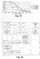
- the invention in another aspects provides a lithography system comprising a charged particle optics column including a blanker for generating charged particle beamlets for projection of a pattern onto a target, a target support, the column and target support being included moveable relative to one another in the system, the system further comprising a data path for processing and transferring pattern data to a blanker of the column, the blanker arranged capable of switching each of the beamlets on and off in respect of projection on the target, the datapath comprising processing units for processing pattern data into projection data related to a stripe on the target forming a projection area of a beamlet at relative movement of target support and column, the data path thereto comprising channels connected to the blanker for individually controlling a beamlet by the projection data, the system further being provided with a switch for switching connection a processing unit between different channels.
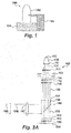
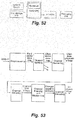
- FIG. 1 is a conceptual diagram showing a charged particle lithography system 100 divided into three high level sub-systems: a wafer positioning system 101, an electron optical column 102, and data path 103.
- the wafer positioning system 101 moves the wafer under the electron optical column 102 in the x-direction.
- the wafer position system 101 is provided with synchronization signals from the data path 103 to align the wafer with the electron beamlets generated by the electron-optical column 102.
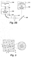
- FIG. 2A shows a simplified schematic drawing of an embodiment of a charged particle lithography system 100 showing details of the electron optical column 102.
- Such lithography systems are described for example in U.S. Patent Nos. 6,897,458 and 6,958,804 and 7,019,908 and 7,084,414 and 7,129,502 , U.S. patent application publication no. 2007/0064213 , and co-pending U.S. patent applications Serial Nos. 61/031,573 and 61/031,594 and 61/045,243 and 61/055,839 and 61/058,596 and 61/101,682 , which are all assigned to the owner of the present application and are all hereby incorporated by reference in their entirety.
- the lithography system comprises a charged particle source 110, e.g. an electron source for producing an expanding electron beam 130.
- the expanding electron beam 130 impinges on an aperture array 111, which blocks part of the beam to create a plurality of beamlets 131.
- the system generates a large number of beamlets, preferably in the range of about 10,000 to 1,000,000 beamlets.
- the electron beamlets 131 pass through a condenser lens array 112 which focuses the electron beamlets 131.
- the beamlets 131 are collimated by collimator lens system 113.
- the collimated electron beamlets pass through XY deflector array 114, a second aperture array 115, and second condenser lens array 116.
- the resulting beamlets 132 next pass through beam blanker array 117, comprising a plurality of blankers for deflecting one or more of the beamlets.
- the beamlets pass through mirror 143 and arrive at beam stop array 118, which has a plurality of apertures.
- the beamlet blanker array 117 and beam stop array 118 operate together to switch the beamlets on or off, by either blocking beamlets or letting them pass.
- the beamlet blanker array 117 can deflect a beamlet so that it will not pass through the corresponding aperture in beam stop array 118, but instead will be blocked. If beamlet blanker array 117 does not deflect a beamlet, then it will pass through the corresponding aperture in beam stop array 118. The undeflected beamlets pass through the beam stop array, and through a beam deflector array 119 and projection lens arrays 120.
- Beam deflector array 119 provides for deflection of each beamlet 133 in the X and/or Y direction, substantially perpendicular to the direction of the undeflected beamlets, to scan the beamlets across the surface of target 104. This deflection is separate from the deflection used by the beamlet blanker array to switch the beamlets on or off.
- the beamlets 133 pass through projection lens arrays 120 and are projected onto target 104.
- the projection lens arrangement preferably provides a demagnification of about 100 to 500 times.
- the beamlets 133 impinge on the surface of target 104 positioned on a moveable stage of the wafer positioning system 101.
- the target usually comprises a wafer provided with a charged-particle sensitive layer or resist layer.
- FIG. 2A The representation shown in FIG. 2A is much simplified.
- a single electron beam is first partitioned into many smaller subbeams which are then split into an even larger number of beamlets.
- Such a system is described in US patent application 61/045,243 , which is hereby incorporated by reference in its entirety.
- each subbeam is split into a number of beamlets which can be considered a patterned beam.
- each subbeam is split into 49 beamlets arranged in a 7 x 7 array.
- the beamlet blanker array preferably comprises one hole with an associated blanker electrode for each beamlet, to enable on/off switching of each individual beamlet.
- FIGS. 3 and 4 show a portion of a beamlet blanker array for an embodiment having 9 beamlets per patterned beam, each group of beamlets arranged in a 3 x 3 array. The arrangement of beamlets in a patterned beam and writing strategies are described for example in US patent application 61/058,596 , which is hereby incorporated by reference in its entirety.
- the beam deflector array and projection lens array preferably include only one hole and lens for each patterned beam (e.g. one hole or lens for each group of 49 beamlets making up one patterned beam). Beamlets are typically combined (interleaved/multiplexed) in a group that writes a singe stripe.
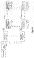
- FIG. 2B A simplified block diagram of one embodiment of a data path 103 is shown in FIG. 2B , and a portion of the data path also appears in FIG. 2A .
- the switching of beamlet blanker array 117 is controlled via the data path.
- a preprocessing unit 140 receives information describing the layout of the device to be manufactured by the lithography machine. This information is typically provided in a GDS-II file format. The preprocessing unit performs a series of transformations of the GDS-II file to generate on/off control signals to control the beamlet blanker array 117.
- the control signals are transmitted to electro-optical conversion devices 143, such as laser diodes, to convert the electrical control signals into optical signals.
- the optical control signals are guided through optical fibers 145.
- the light beams 146 at the output of the fibers are guide through an array of lenses 147 onto a holey mirror 148. From the mirror, the light beams are reflected onto the underside of beam blanker array 117.
- the individual light beams are directed onto a plurality of optical-to-electrical conversion devices, such as photo diodes, on the underside of the beam blanker array 117.
- the photo diodes operate to activate the individual beam blanker electrodes to control the deflection of beamlets 132 to switch the individual beamlets on or off.
- the control signals for controlling the individual beamlet blanker electrodes are preferably multiplexed, so that each light beam 146 carries control signals for a channel comprising a number of beamlets that share one optical fiber and photo diode.
- the multiplex light beams are received by photo diodes and converted into an electrical signal.
- the beamlet blanker array 117 includes logic for demultiplexing the control signals received by the photo diodes to derive control signals for individually controlling a number of beamlet blanker electrodes.
- individual control signals for controlling 49 beamlets of one patterned beam are time multiplexed for transmission over a single optical fiber, and are received by a single photo diode on the beamlet blanker array.
- the beamlet control signals may also be arranged in frames for transmission and may have synchronisation bits and additional encoding to improve transmission, e.g. using an encoding technique to achieve frequent signal transitions, to prevent using the laser diodes and photo diodes in a DC-coupled fashion. By forcing transitions, the clock signal is automatically distributed in the optical signal.
- FIG. 12 shows an example of a beamlet control signal with framing, synchronisation bits, and multiplexed control bits for 49 beamlets (of one patterned beam).
- the beam deflector array 119 is used to deflect the electron beamlets in the y-direction (and also a small deflection in the x-direction) to achieve scanning of the electron beamlets over the surface of the wafer 104.
- the wafer 104 is mechanically moved in the x-direction by the wafer positioning system 101, and the electron beamlets are scanned across the wafer in a y-direction substantially perpendicular to the x-direction.
- the beamlets are deflected slowly (compared to the fly-back time) in the y-direction. At the end of a sweep, the beamlets are moved quickly back to the start position of the y-range (this is referred to as the fly-back).
- the beam deflector array 119 receives timing and synchronization information from the data path 103.
- the data path may be divided into a number of channels.
- a channel is an electronic data path from the preprocessing unit to the lithography system.
- a channel comprises an electrical-to-optical converter (e.g. a laser diode), a single optical fiber for transmitting beamlet control signals, and an optical-to-electrical converter (e.g. a photo diode).
- This channel may be assigned to transmit the control signals for a single patterned beam comprising a number of individual beamlets (e.g. 49 beamlets making up one patterned electron beam).
- One patterned beam may be used for writing a single stripe on the wafer.
- a channel represents the data path components dedicated to control of one patterned beam comprising multiple beamlets (e.g. 49 beamlets) and carrying the beamlet control signals for writing one stripe according to the pattern data.
- a subchannel represents the data path components dedicated to control of a single beamlet within a patterned beam.
- the data path 101 transforms the layout data into on/off signals for controlling the electron beamlets.
- this transformation may be performed in a preprocessing unit 140 performing a series of transformations on the layout data, typically in the form of a GDS-II or similar file. This process typically includes flattening/preprocessing, rasterization, and multiplexing steps.
- the flattening/preprocessing step transforms the layout data format into a dose map.
- the dose map describes areas on the wafer in vector format and associated dose rate values.
- This step may include some preprocessing such as proximity effect correction. Because of the complexity of the preprocessing, this step is preferably performed offline.
- the rasterization step transforms the dose map into a stream of control (on/off) signals.
- the multiplexing step packages the beamlet control signals according to a multiplexing scheme.
- a wafer 104 is installed on the stage of the wafer positioning system 101, the column 102 is maintained in vacuum conditions, and the beamlets are calibrated. The wafer is aligned mechanically, and per field alignments (offsets) are calculated. The wafer is moved in the +x-direction by the stage and the column starts writing the first field. When the leading row of holes of the beamlet blanker array passes a field boundary, offset corrections are installed for the next field. Thus, while the first field is still being written, the lithography system will start to write the next field.
- the stage After writing the last field in a row, the stage will move to position the next row of fields on the wafer under the beamlet blanker array. A new run will start while the stage moves in the -x-direction.
- the direction of the scan deflection preferably does not change.
- the data processing performed by the data path may provide for a number of different adjustments to the beamlet control signals to make various types of corrections and compensations. These may include, for example, proximity correction and resist heating correction to compensate for effects occurring as a result of the properties of the resist used.
- the data adjustments may also include corrections which are designed to compensate for errors or failures occurring in the lithography machine.
- the charged particle lithography machine there are no facilities built into the lithography machine for adjusting individual electron beamlets to correct for errors in beamlet position, size, current, or other characteristics of the beams. Faults such as misalignment or failure of a beamlet, low or high beamlet current, incorrect deflection of the beamlet. Such faults can be the result of defects or tolerance variations in the manufacturing of the lithography machine, dirt or dust blocking beamlets or becoming charged and deflecting beamlets, failure or deterioration in the components of the machine, etc.
- the lithography machine omits corrective lenses or circuits for making individual corrections to beamlets to avoid the additional complexity and cost involved in incorporating additional components into the electro-optical column for making physical beam corrections, and to avoid the increase in size of the column necessitated by incorporating such additional components.
- manipulation of the beamlet control signals and/or additional scans of the wafer can compensate for these types of problems. Failures occurring in the data path may also be corrected by manipulation of the control signals in conjunction with rescanning the wafer.
- Various methods for making these corrections are described below.
- the embodiment of the charged particle lithography machine described above has a large number of optical fibers and laser diodes in the data path, a large number of electrostatic lenses and deflectors for each patterned beam, and a very large number of blanker elements in the beamlet blanker array. There is a significant chance that a failure may occur in some of these components or that they will deteriorate or be affected by contaminants so that they do not perform within specification.
- a check may be performed periodically to identify failing or out of specification beamlets or data channels. This check may be performed before each wafer scan, before each first scan of a wafer, or at some other convenient moments.
- the check may include one or more beam measurements, including for example as described in co-pending US application 61/122,591 , which is hereby incorporated by reference in its entirety.
- the primary goal of the redundancy scan is to compensate for failures occurring in the EO column, since replacement of failed parts in the column is time consuming.
- the redundancy scan may also be used to cope with failures in the data path. For example, a failed optical fiber of laser diode in one channel may be corrected by switching that channel off and using another channel during the redundancy scan to write the stripes that would have written by the failed channel.
- the beamlet may be switched off so that the stripe that would have been exposed by that beamlet is not written.
- a second scan referred to as a redundancy scan, is then used to write the wafer stripe that was omitted during the first scan.
- the complete channel that includes the failed or out-of-spec beamlet may be switched off, and the complete stripe of the wafer field that would have been exposed by the beamlets of that channel will not written.
- a redundancy scan may then be performed to fill in the missing stripe (and any other missing stripes for other channels with failed beamlets).
- the wafer is returned to the starting position after the first scan, but also shifted to a position which ensures that properly functioning channels are available for writing the missing stripes.
- the pattern data for the redundancy scan is preferably prepared in the lithography system during the first scan to enable the redundancy scan to begin as soon as possible after completion of the first scan. There is preferably no significant delay between the end of the first scan and the start of the redundancy scan, so data for the redundancy scan is preferably available quickly on the appropriate node.
- the lithography machine is preferably able to write successive in-line fields in one scan, and write in both directions in an x-direction parallel with the mechanical scan, i.e. -x and +x direction.
- the machine also preferably includes spare beams (or patterned beams), usually located at the edges of the column.
- the wafer may be shifted (offset) with respect to the column in the y-direction and/or x-direction an amount corresponding to a number of stripes until channels with properly functioning beamlets are positioned to write the missing stripe positions. This is preferably accomplished by a mechanical offset of the wafer on the stage. To deal better with all kinds of error positions (e.g. failure of both the first and last channel), an offset for both the first and the second scan may be required.
- a second scan can also be used to augment the first scan for functioning beamlets as well as defective beamlets in a "multi-pass scan" embodiment, while still achieving the redundancy scan function.
- a multi-pass scan the first scan of the wafer writes a portion of the field stripes and a second scan writes the remaining portion of the stripes, to result in writing all of the stripes of each field of the wafer.
- This principal can also be extended to three scans or four scans etc., although a greater number of scans increases the total time for exposing the wafer and reduces wafer throughput.
- a two-pass scan or dual scan approach is preferred.
- a beam measurement may be performed before the first scan to detect failed and out-of-specification beamlets.
- a first and second scan can be calculated that will result in every pixel of the wafer being assigned for scanning by functioning beamlets.
- the redundancy scan preferably when a failed or out-of-spec beamlet is detected, the entire channel that includes that beamlet is switched off and another functioning channel (with all beamlets in-spec) is used to write the stripes that would have been written by the failed channel.
- Various algorithms may be used to calculate the channels to be used for the first and second scans and the wafer offset required for each scan, to result in all stripes being written by functioning channels. For a two-pass scan, the algorithm looks for a 50/50 split of channels between each scan that does not use any channels. A "brute force" approach could be used to test various channels allocations and wafer offsets to find a suitable combination, or more sophisticated matching algorithms could be used.
- the total exposure current for the wafer is divided between two (or more) scans.
- the second scan (or third scan or fourth scan etc.) may be used to scan stripes that were assigned to a failed channel in the first scan, as in the redundancy scan.
- the multi-pass scan can also be used in the absence of any failed or misaligned beamlets. Dividing the exposure current over two or more scans has the advantage that instantaneous heating of the wafer becomes less of a problem. Because the total beamlet current for each scan is reduced, the heating imparted to the wafer by each scan is also reduced. Although the total heat load remains substantially the same, it is spread over multiple scans resulting in less localized or instantaneous heat load.
- the current industry standard is a 300mm wafer.
- the wafers are divided into fixed size fields with a maximum dimension of 26mm x 33mm.
- Each field may be processed to produce multiple ICs (i.e. the layout for multiple chips may be written into a single field) but the ICs do not cross a field border.
- With a maximum size of 26mm x 33mm there are 63 fields available on a single standard wafer. Smaller fields are possible and will result in a higher number of fields per wafer.
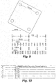
- FIG. 5 shows a wafer divided into fields, and the direction of writing the fields.
- a field is a rectangular area on a wafer, typically with a maximum size of 26mm x 33mm.
- a GDS-II file describes the features of a field. It is also possible to write partial (incomplete) fields, for example by writing full fields into the partial fields and crossing the wafer boundary.
- the machine In a preferred embodiment of the lithography machine, the machine generates 13,000 subbeams and each subbeam is split into 49 beamlets, resulting in 637,000 beamlets (i.e. 13000 x 49).
- the beamlet blanker array contains 13,000 photo diodes and 637,000 holes in an area of 26x26mm. Each photo diode in the beamlet blanker array receives a multiplexed control signal for control of 49 (7x7) blanker holes/beamlets.
- the 13,000 subbeams over a distance of 26mm result in a stripe of width 2 ⁇ m in the y-direction (perpendicular to the mechanical scan) and as long as the field in x-direction.
- the 49 beamlets of each subbeam write a single stripe.
- the wafer is preferably written on (exposed) by the lithography machine in both a backward and forward x-direction.
- the direction of writing in the y-direction (by the deflector) is usually in one direction.
- the size (height) of a field is chosen to be smaller than the size of the electron-optical (EO) slit (i.e. the size of the complete array of beamlets as projected onto the wafer) (e.g. smaller than the maximum size of 26mm), then more fields can be placed on the wafer, but not all of the electron beamlets will be used to write on the wafer.
- the EO slit will need to scan the wafer more times and the overall throughput will decrease.
- the beamlet blanker array When a machine is writing patterns to a field, at some moment the beamlet blanker array enters the next field and starts writing patterns in it, so the machine should be able to write in two fields at the same time. If a field is sufficiently small, the machine should be able to write 3 fields at the same time.
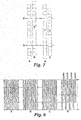
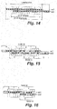
- FIGS. 3 and 4 A simplified version of a beamlet blanker array is shown in FIGS. 3 and 4 , with only 16 photo diodes that each receive a multiplexed control signal for control of 9 (3 x 3) blanker holes/beamlets.
- a blanker hole with an associated blanker electrode is able to block or pass through a beamlet (electron beam).
- a beamlet passing through the blanker hole will write on the resist on the wafer surface.
- FIG. 3 an arrangement of blanker holes is shown for a parallel projection writing strategy, while in FIG. 4 this is shown for a perpendicular writing strategy.
- the blanker holes for the beamlets are distributed over the full stripe width, i.e. each beamlet is positioned equidistant from the neighbouring beamlets in a direction perpendicular to the writing (scan) direction.
- a measure for the efficiency is the fill factor, which is the ratio between the total area of the blanker holes and the area in which the holes for one patterned beam are grouped.
- the fill factor is useful for evaluating the efficiency of a particular grid geometry in terms of current in (beam current) and current out (sum beamlet currents). When the area of the group of beamlet holes is smaller, the fill factor will increase to more preferred values.
- a writing strategy that works well for a small number of holes is the "parallel projection" writing strategy (see FIG. 3 ), where (in its simplest form) the individual beamlets are interleaved and write the full stripe width (as shown in FIG. 8B ).
- Such a writing strategy is described in US patent application 61/058,596 , which is hereby incorporated by reference in its entirety.
- the beam deflector array 119 will generate a triangular shape deflection signal for all beamlets in parallel.
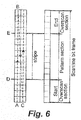
- the deflection signal includes a scan phase and a fly-back phase, as shown in the schematic diagram in FIG. 6 .
- the deflection signal slowly moves the beamlets (when switched on) in the y-direction and the beamlet blanker array will switch the beamlet on and off according to the beamlet control signals.
- the fly-back phase starts.
- the beamlet is switched off and the deflection signal quickly moves the beamlet to the position where the next scan phase will start.
- a scan line is the path of a beamlet on the surface of the wafer during the scan phase. Without special measures the scan line would not write exactly along the y-direction on the wafer, but will be slightly skewed with a small x-direction component as well because of the continuous stage movement in the x-direction.
- This error may be corrected by adding a small x-direction component to the deflection field to match the stage movement. This correction may be dealt with in the EO column so that the data path does not need to correct for this error.
- This x-direction component is small because the stage movement is slow in comparison to the y-direction deflection scan speed (a typical x:y relative speed ratio may be 1:1000).
- the effect of this x-direction component is greatly increased in systems with patterned beams.
- the deflection speed may be reduced in proportion to the number of beamlets per patterned beam.
- a skew in the scan lines on the wafer will result in altering the distance between scan lines made by different beamlets.
- a large enough skew may result in scan lines overlapping or changing position with respect to each other.
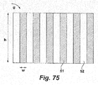
- a scan line (see FIG. 6 at the right) is divided into three sections: a start overscan section, a pattern section, and an end overscan section. Beamlets are deflected along the y-direction. The distance in which the beamlets are deflected is typically wider than its stripe should write. Overscan provides space for shifting and scaling the positions where the beamlet writes. Overscan is the single sided surplus. In case of a stripe width of 2pm and an overscan of 0.5pm (or 25%) this results in a scan line length of 3pm.
- the overscan sections of the scan line bit frame hold the bits that are not used for writing a pattern (pattern section bits). Overscan bits are always switched off, but transmitted over the fiber.
- the pattern section of the scan line bit frame holds the bits that describe the rasterized pattern. In this section the bits are actively switched on and off for writing features.
- FIG. 6 (at the left) a scan line is depicted for the situation where only one beamlet is writing a stripe.
- the path of the beamlet during a deflection cycle is A-B-C.
- AB is the scan line movement during the scan phase, while BC is the fly-back during which the beamlet is switched off.
- the stripe borders are marked D and E.
- the overscan and pattern sections are identified.
- the total set of bits of the beamlet control signal for switching the beamlet over the scan line is called the scan line bit frame.
- the beamlets are controlled by the lithography system.
- the overscan section the beamlets will be switched off.
- the pattern section the beamlets are switched according to the features required to be written in the wafer field.
- the bits in the scan line bit frame for both the overscan section and pattern section represent the data to be transferred to the beamlet blanker array.
- the bits/pixels in the overscan section seem to be useless and consuming bandwidth of the data path.
- the bit/pixels in the overscan section can provide room for corrections (such as pattern shift and pattern scaling), provide room for stitching algorithms, and provide room for differences in y-positions of blanker holes for beamlets when writing strategies are used where all beamlets write the full stripe width (parallel projection).
- the scan line can be mapped into a fixed length bit frame, the scan line bit frame.
- Scan line A is a normal scan line without offset or scaling, where the beamlet writing the scan line is correctly aligned and correctly deflected to expose the desired feature correctly on the wafer.
- Scan line B is not optimally aligned with the stripe, e.g. due to misalignment of the beamlet. This can be corrected by adjusting the timing of the beamlet switching, by shifting the data in the beamlet control signal by one full pixel. This can be accomplished by shifting the control bits inside the scan line bit frame.
- Scan line C is not scaled correctly to fit within the stripe boundaries D and E, e.g. due to deflection of the beamlet that is locally weaker than normal. Therefore the pattern section consumes more bits of the control signal, while the overscan sections use less.
- the pattern to write the stripe needs more bits for the stripe width. From a bit frame point of view, shifting and scaling can only be done in full pixel resolution. However, the rasterization process is able to deal with subpixel resolution corrections (e.g. 0-1 pixel). Combining the two will give allow for shifts such as a shift of 2.7 pixels.
- each subbeam is split into 49 beamlets and a channel combines 49 beamlets for writing a stripe.
- the beamlet writing strategy defines in what way the beams are arranged for writing a stripe.
- the scheme could be combinations of stacking, interleaving or overlapping.
- Beamlets are deflected in two phases: scan and fly-back. During the scan phase, a beamlet is deflected (when it is switched on) along its scan line over the wafer. The pattern section of the scan line bit frame will be filled with the bit pattern for exposing the desired chip features.
- FIG. 8 several examples are shown as possible interleaving schemes for writing a stripe using four beamlets. These examples do not show how the beamlets write in real-time, but show which beamlet has written which part of the stripe when the writing has finished.
- Example A shows stacking the beamlets. Every beamlet writes in its own substripe. For this configuration each beamlet only writes a small number of bits before it flies back.
- the frequency of the deflection signal is high and its amplitude is low.
- This writing strategy is suited to the case where the beamlets in a group are arranged so that the group width (number of beamlets N x projection pitch Pproj) is equal to the stripe width (perpendicular projection).
- Perpendicular projection is a family of writing strategies. For the basic form of perpendicular projection all beamlets write small substripes. The width of the substripe is a fraction of the stripe width. The size of the grid of blanker holes is typically related to the stripe width.
- the beamlets are interleaved over the full stripe width.
- the frequency of the deflection signal is low and its amplitude is large.
- the write strategy that fits with the interleaving scan lines is the parallel projection write strategy. Especially for a relatively low number of beamlets in a group, this strategy allows for a smaller group size and an improved fill ratio. Because of the small number of beamlets, the size of the group on the wafer is significant smaller than the stripe because of a reasonable fill factor.
- this write strategy parallel projection
- Parallel projection is a family of writing strategies. For parallel projection all beamlets write the full stripe width in an interleaved way. The grid of blanker holes is not related to the stripe width.
- Example C is a combination of interleaving and stacking.
- D the successive interleaved layers are overlapping like a brick wall.
- this configuration will provide better averaging between beamlets.
- At the stripe boundary there are beamlets that would write over the stripe boundaries.
- FIG. 8 shows an example of how the scan lines fill the stripe.
- the writing strategy determines how the scan lines will be written using the pattern of holes for the beamlets on the beamlet blanker array.
- One advantage of the "parallel projection" writing strategy is its efficiency.
- One electron beam is used to make the beamlets. Its efficiency depends on the ratio of the total area of holes (beamlets output current) compared to the area of the group of holes (beam input current). For a relative small number of holes (49), the area of the beam (group of beamlets) must be small for an acceptable efficiency.
- the beam (group) size is smaller that the stripe width.
- the pixel size is an important system parameter. The relation between the blanker grid (of holes) and the pixel size is explained below.
- FIG. 9 shows a simplified beamlet blanker array. For each beamlet there is a corresponding hole in the beamlet blanker array, and a blanker electrode at each hole.
- the blanker includes electronics to switch the beamlets off or on by energizing or de-energizing the blanker electrodes.
- an array with only four holes is shown and the patterned beam consists of four beamlets.
- K is a factor relating to the distance between scan lines, e.g. caused by movement of the stage between scans. Different K factors can be achieved by adjusting the relative speed of stage movement in the x-direction and deflection speed (scan phase and a fly-back phase) in the y-direction.
- the pattern is shown that will be written when the stage moves the distance of the group width.
- the distance between the scan lines is equal to the distance between the blanker holes for this projection, i.e. the projection pitch (Pproj).
- the projection pitch will be much larger than the pixel size and is a constant (design parameter of the lithography machine).
- the other rows in FIG. 9 show what happens to the scan line distance in the x-direction when the stage moves only an integer fraction of the group size. K is this fraction.
- FIG. 66 illustrates the possible values of K for a patterned beam having 4 beamlets.
- FIG. 11 is a diagram of an array of nine beamlets showing the definitions of some of the terms used, including beam pitch P b , projection pitch P proj , grid width W proj , and tilt or inclination angle ⁇ array .
- FIG. 63 is another example showing an array of four beamlets.
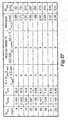
- FIG. 57 shows a table of pixel size and grid width in dependence on the number of beamlets per patterned beam (N pat_beams ), the array tilt angle ( ⁇ array ), the projection pitch (P proj ), and K factor.
- N pat_beams the number of beamlets per patterned beam
- ⁇ array the array tilt angle
- P proj the projection pitch
- K factor K factor
- the closest value of K which is acceptable given the number of beamlets per patterned beam is shown in the fifth column from the left.
- the sixth and seventh columns show the pixel size and grid width in nanometers the will result for the given number of beamlets per patterned beam, array tilt angle, projection pitch, and K factor.
- a higher K indicates a faster deflection scan speed (relative to stage movement), and results in a smaller pixel in the x-direction.
- the pixel will become bigger in the y-direction, so that the pixel shape changes from approximating a square to a rectangle.
- the beamlets are oriented at an angle to the EO-slit to be able to write non-overlapping scan lines.
- the tilt of the EO-slit with respect to the deflection direction causes a position difference in the y-direction, as shown in FIG. 11 .
- This position difference may be corrected for.
- the value for the shift is a multiple of the projection pitch.
- the difference between the top hole and the center hole equals W proj/2 .
- successive control bits sent over each fiber are used for controlling successive blanker holes of the beamlet blanker array (i.e. for controlling a series of beamlets).
- each fiber comprises a channel transmitting control information for 49 subchannels, for control of 49 beamlets on a single patterned beam. This control information can first be buffered before being applied to the blanker electrodes for each beamlet, or the control information and be applied directly without buffering. A buffer could be provided on the beamlet blanker array for this purpose.
- a schematic diagram of a data path with interleaved/multiplexed subchannels is shown in FIG. 55
- a schematic diagram of a demultiplexing scheme is shown in FIG. 56 , using row-selectors and column selectors to decode the multiplexed subchannel to separate the individual control bits for each beamlet.
- frame start indicator bits (in this example 7 bits) are used in a recurring pattern to which a framer on the beamlet blanker will synchronize.
- some kind of encoding is preferably used.
- One example is for instance 8b/10b coding. This will however result in a higher bitrate, with 8/10 bit coding adding 25% to the bitrate.
- Framing and encoding of the signal can also be combined, e.g. by using specific encoded words to mark the start of a frame.
- Each channel will carry data for a number of individual beamlets (e.g. 49 beamlets).
- the information will be transmitted in a serial manner from the data path to the blanker.
- Synchronization of the beamlets may be performed in different ways, for example synchronize all beamlets to one synchronization signal, synchronize all beamlets in a column, synchronize all beamlets in a row, or do not synchronize the beamlets.
- the control data for 49 beamlets may be buffered and applied synchronously to each of the 49 blanker electrodes for switching the beamlets.
- the control data for 7 channels in a each column may be buffered and synchronously applied to the 7 blanker electrodes for that column of beamlets.
- control data for 7 channels in a each row may be buffered and synchronously applied to the 7 blanker electrodes for that row of beamlets.
- control data of all 49 beamlets may be directly applied to the blanker electrodes as the data is received by the blanker.
- stitching is preferably used between parts of the field written by the different beams.
- a stitching error shift of the pattern written by one beam with respect to the pattern written by the neighboring beam
- CD critical dimension
- overlay error 5 nm is typically allowed.
- the stitching approaches are methods to get rid of the CD error resulting from stitching errors. Different stitching strategies may be used. These are, for example no stitiching, ragged edges, soft edges, and smart boundaries.
- FIG. 58B shows a diagram illustrating a soft edges strategy.
- the patterns fade out (before dithering) at both ends where two beams write.
- This strategy has the effect that errors are spread over an area, shown as the 1 ⁇ m soft edge in the diagram.
- a side-effect of this strategy is that certain pixels could be written double (i.e. with 200% dose). Because of the relatively large beam size, the dose will be spread among several pixels.
- FIG. 58A shows a diagram illustrating a smart boundary strategy.
- a 100nm overlapped write range is used, e.g. 25 pixels with 4nm pixels.
- Critical parts of the features of the pattern data at or near the boundary between two stripes or fields will be identified and placed into one stripe or the other. This results in the actual writing boundary between two stripes being moved to avoid crossing a critical part of a feature, so that critical features will always be written by a single beam.
- a soft edge stitching strategy is where both boundaries fade out smoothly into the area of the next stripe.
- the total dose error budget may be set to 3%, and 0.5% dose error is a reasonable budget to give to stitching errors from this dose error budget.
- the stitching methods (soft edges or smart boundaries) and the overscan length may be selection per scan. Reducing the overscan length would result in a higher throughput of the machine.
- the user is preferably able to select either the soft edges or smart boundary stitching strategy and the size of the soft edge.
- a channel is a unit of work in the data path.
- a channel is able to write one stripe during a scan.
- the elements of the data path involved in real-time processing are: fast memory, processing unit, laser, fiber, and blanker. Because only 50% of the channels are active for one scan, the number of processing units might be reduced by approximately the same factor.
- Reduction of the processing units streaming fewer channels at the same time has the following advantages: less logic cells required per channel, hard limit on fast memory bandwidth required per node of channels, and a possible reduction of fast memory storage size required. Reducing the number of processing units also has disadvantages: there must be a way to connect the processing units and the laser for the appropriate channel, and a new constraint might let scans fail, especially in case of a large number of subsequent (cluster) channel errors.
- a node has Y (optical) channels connected and has available X processing units.
- FIG. 13 shows a model for such a node.
- the E/O converter e.g. laser diodes
- the processing units e.g. field programmable gate arrays, FPGA's
- driving the E/O converters contain X number of channels.
- An X * Y crosspoint may be used to switch any of the processing units to any of the O/E converters.
- the X * Y crosspoint is a separate device or is integrated in the processing units. With the crosspoint it is possible to route any of the processing unit outputs (X) to any of the data path outputs (Y).
- first the possibilities for a shift between the first and second scan need to be determined where all stripe positions are covered by at least one proper working channel.
- possible shift positions are known, it is determined whether the available processing units are allocated between the scans and cover 100% of the stripes.
- FIG. 14 the channel positions per scan are shown in a conceptual diagram.
- the stripes as shown in FIG. 14 (blue) are written with this particular combination of channel errors and the two individual shift values. It is important to distinguish between overlapped and non-overlapped channel positions. For a stripe at an overlapped channel position to be written correctly, a working channel at this position for one of the scans must available. For non-overlapped channel positions, a shift of the wafer between the first and second scan will result in two regions where it is only possible to write the stripe in one particular scan. A failed channel in this region will break the sequence of good channels. The left most channel error (see red arrow pointing to it in the figure) forces the stripes to start at its right side. At the left the channels cannot be used. Typically shifting is used to get the overlapped region to be free of errors (using two scans) and some channels in the overlapped region may be used to reach the required number of stripes to write.
- the probability of not being able to write a position in the non-overlapped region is relatively high compared to the probability of not being able to write a position in the overlapped region. Therefore typically the sequences of "good channels" in the non-overlapped region are short. Therefore covering 13000 stripes in two scans using 12870 channels will be difficult because it depends too much on the availability of relatively large sequences of good channels in the non-overlapped regions. Covering 13000 stripes in two scans using 13130 channels will be much easier because its success will not depend much on the non-overlapped regions. In practice it is likely that the full sequence of stripes is found in the overlapped region.
- FIG. 15 an example of this is shown. For this example we assume nodes that manage 5 channels and 3 processing units. The white dots indicate that channels are switched off, while black dots indicate channels that are used and a processing unit is allocated. The red cross indicates channel errors. One can verify that no node violates the constraint of having maximum three processing units active in a node for a particular scan.
- FIG. 16 shows a consequence of using less processing units than channels for the non-overlapped regions.
- the drawing shows the maximum sequence of good channels is obtained with the constraint of three processing units per five channels for a node.
- the maximum length equals two times the number of processing units per node.
- the useful sequence in the non-overlapped region will be substantial smaller (see what happens when the shift is increased by one).
- the channels in the non-overlapped region are even less useful than before (not considering reducing the amount of processing units).
- Key parameters for the concept of a redundancy scan are the number of stripes, number of channels, expected number of error channels, expected size of error clusters, number of channels per node, and number of processing units per node.
- a 'good' sequence consists of either 'good' channel positions in non-overlapped regions or positions in the overlapped regions where at least one of the channels is 'good'. This process will result in a list of shifts and the start and size of the 'good' region.
- a possible allocation strategy first allocates channels that must write certain stripe positions. These positions typically are positions in non-overlapped regions and positions in overlapped regions of one scan that correspond to error channels in the other scan. In case any node needs more processing units than available, the allocation attempt will fail.
- the allocation proceeds iteratively through the stripe positions. Processing units are allocated from nodes that will leave scope the earliest. In case such a node is fully allocated, the node from the other scan should allocate a processing unit for writing the position. In case any node needs more processing units than available, the allocation attempt will fail. Other strategies may be used that deliver better results, finding allocation possibilities in cases previously rejected.
- spare processing units are processing units in excess of half of the number of channels a node should serve, e.g. a configuration of 12 channels per node and 6 processing units has no spare processing units.
- FIGS. 17-23 are graphs illustrating the result of simulation experiments to determine the effect of varying the capacity of the data path in relation to the capacity of the lithography machine.
- the graphs show the number of successes out of the 50 experiments.
- Nodes of 12 channels using 7 processing units are referred to as a 12/7 configuration.
- FIG. 17 the effect of different number of processing units per node is shown, assuming no large error clusters (only small natural clustering).
- the 12/6 configuration is the lower limit considered for the reduction because the configuration of 5 processing units per 12 channels will always fail.
- the 12/12 configuration effectively is the configuration without any reduction of processing nodes. Its success only depends on finding a successful shift (no allocation restriction). The simulation results show that the robustness will slightly decrease for the 12/6 and 12/7 configurations compared to the 12/12 configuration.
- FIG. 18 focuses on the effect of error clusters on the same configurations as in FIG. 17 .
- the 12/6 configuration is particularly sensitive for error clusters of size 5, caused by the lack of spare processing units in the nodes. One error at a critical location will cause the failure of the run.
- the 12/7 and 12/12 configurations do not show a particular sensitivity for clusters of size 5.
- FIG. 20 shows the results when the previous simulation is extended with the effect of error clusters of 5. No significant effect is observed in combination with varying the number of channels.
- FIG. 21 presents the results when trying to compensate for the loss of robustness due to the reduction of processing units by using more channels.
- the loss of robustness when changing the configuration from 12/12 to 12/7 can be compensated by increasing the number of channels by only about 1% (e.g. increasing the number of channels from 13130 to 13280).
- FIG. 22 shows a comparison of three strategies: inject a single cluster only; inject as many as possible similar clusters at regular distances (65 from start position to start position); and inject as many as possible similar clusters at random positions (however maintaining a minimum distance of 20 good channels in between them). Note that the fixed distances between the error clusters create a lot of correlation and will result in a large amount of successful shifts.
- Clusters bigger than the size of 5 will have a serious impact on robustness when reducing the number of processing units. This can be seen in FIG. 23 where the difference in robustness between the 12/07 with cluster size 5 (12/07@5) and 12/7 with cluster size 8 (12/07@8) is apparent.
- Randomizing channels over the nodes, or systematically distributing the channels widely among the nodes, are other alternatives. These will result in an error cluster corresponding to many different nodes, rather than being concentrated in one or two nodes. Writing all the mirror positions of the cluster errors will in this configuration not be the responsibility of 1 or 2 nodes, but many of them. However, randomizing or dispersing channels might however have other negative side effects because the concept of a neighbor (and potentially sharing information) disappears.
- Allocation strategy optimization besides checking allocation constraints, an important task of the allocation functionality could be to minimize the number of stitches between the scans.
- the flow diagram in FIG. 24 shows an overview of the processes involved in the lithography system and their dependencies. Understanding the dependencies permits an analysis of performance (in terms of duration) and reveals opportunities for parallel execution to increase throughput. An important principal is that pattern data for a scan may be processed and/or loaded into RAM while the previous scan is executed.
- the clock and synchronization signal may be distributed to the other sub-systems (such as deflector and wafer stage) over an optical fiber.
- This has the advantages of galvanic isolation between the sub-systems and insensitivity to electromagnetic influence.
- Clock variation can be used to vary dose. However, as dose-variations can be compensated for by changing the pixel size, clock variations are preferably avoided to simplify the implementation of the physical part of the data path responsible of transmitting the data to the blanker and eliminate the time needed to re-synchronize after a change in clock frequency.
- the data path preferably operates as the clock master for the complete lithography system and will provide timing and synchronization signals to the other sub-systems such as the electron-optical column (deflector) and wafer positioning system.
- the charged particle lithography machine In the embodiment of the charged particle lithography machine described above, these are no facilities built into the lithography machine for adjusting individual electron beamlets to correct for errors in beamlet position, size, current, or other characteristics of the beams.
- the lithography machine omits corrective lenses or circuits for making individual corrections to beamlets to avoid the additional complexity and cost involved in incorporating additional components into the electro-optical column for making physical beam corrections, and to avoid the increase in size of the column necessitated by incorporating such additional components.
- the pattern data is adjusted to compensate for the alignment errors.
- This adjust may be made using software or hardware, and can be done at different stages during processing of the pattern data.
- the corrections can be made to the pattern data in vector format, or in multi-level gray scale format, or in the two-level B/W bitmap.
- Offsets may occur in the x-direction (direction of stage movement) or y-direction (direction of beamlet scan deflection) or both. Offsets may occur in a full pixel shift and/or subpixel shift. A full pixel shift may be achieved by shifting a number of pixels after rasterization. A subpixel shift can be achieved as part of the rasterization process.
- Global pattern shifting i.e. a shift of all beamlets in a channel
- stripe position correction in x- and y-direction
- field position correction in x- and y-direction
- An example of an x and y pattern shift for stripe position correction is shown in FIG. 25 .
- a stripe On the left of the drawing, a stripe is shown with the desired pattern overlaid in the intended position.
- a stripe is shown with a pattern overlaid as it would be written if no correction was made.
- a global pattern shift is required to cause all beamlets of the channel to write in a position shifted up and to the left.
- Beam offsets are typically done frequently after calibration (once per wafer or field). It can be assumed that beamlets are aligned perfectly with respect to the other beamlets in the same channel, so that all beamlets in a channel get the same pattern offset.
- Typical requirements for pattern shifting are individual X and Y shift settings per channel for global shifting, and a parameter update once per field.
- a typical maximum shift range may be +200nm to -200nm, with a shift accuracy of 0.1 nm. This correction is per channel for global shifts because it is expected that all beamlets in a patterned beam use the same offset values.
- the channel pattern is shifted as a whole independent of the beam interleaving strategies.
- Blanker timing offset correction requires correction in Y per subchannel, typically with maximum shift range less than one pixel, and shift accuracy of 0.1 nm.
- the shift parameter is static, since the blanker timing offset depends on the blanker design.
- Blanker hole offset correction requires correction in Y for the subpixel component per subchannel, typically with a maximum shift range of +/- Wproj/2 or +/-210 ⁇ m (i.e. (N-1) * Pproj), and shift accuracy of 0.1 nm.
- the correction parameter is static, beacsue blanker hole offset is a function of the blanker geometry.
- the effective dose varies per beamlet. Variations in beamlet scan deflection strength can also result in a variation of dose intensity.
- Dose correction is performed per beamlet, with correction parameter update once per wafer.
- Typical requirements/values for dose correction are a pattern dose map of 50% - 100%, pattern dose accuracy of 0.2% step size, beam dose factor of 80% - 100%, and beam dose accuracy of 0.2% step size.
- the resulting dose rate should be rounded to the nearest value.
- Beams are deflected during each scan in the y-direction and write a pattern from one side of the stripe to the other side.
- the deflection distance preferably covers both the stripe width and two times the overscan distance. In case the deflection is not perfectly uniform, one beam is deflected stronger than others and therefore deflection distances will be different. Differences in the strength of the scan deflection occur over the surface of the scan deflection array due to voltage drops occurring across the array. These voltage drops result in a weaker deflection field at the far ends of the array, and the deflection distance will be shorter for beamlets experiencing the weaker deflection fields.
- FIG. 26 An example of pattern scaling is shown in FIG. 26 .
- a stripe On the left of the drawing, a stripe is shown with the desired pattern overlaid with the intended scaling of the pattern feature between the dashed lines.
- a stripe On the right of the drawing, a stripe is shown with a pattern overlaid as it would be written if no scaling correction was made.
- a pattern scaling correction is required to reduce the deflection of all beamlets of the channel to write the feature with the correct scaling.
- Scaling may be accomplished by adjusting the bit rate of the data signal transmitted to the blanker, spreading the exposure pattern over a different number of pixels. Due to synchronization considerations, changing the bit rate is not preferred. To avoid this, scaling may be done by spreading the pattern over a different number of bits/pixels. It is assumed that the beamlets of the same group have the same deflection strength. This is because they are deflected by the exact same deflector. The pattern scaling factor is thus the same for all beamlets of a certain group.
- Pattern scaling requires correction per channel, with correction parameter update preferably once per redundancy scan reshuffle.
- Deflection strength is assumed to be the same for all beamlets in a channel because the beamlets share the same deflector array, and are more or less in the same position in this deflector.
- FIG. 27 is a table summarizing various types of corrections and typical parameters and ranges. Note that when both a first scan and a second (or redundancy) scan are used, dose corrections are preferably performed before both scans.
- Dynamic pattern shifting may also be provided, to compensate for wafer heating. This can be accomplished using an X and Y offset table per channel with values varying as function of time. Maximum slope of 0.1 nm per 1ms (equals -10 ⁇ m in X) may be used, and an offset table with 30,000 entries per 300 mm (wafer size).
- the deflection distance of beamlets will vary. This may be compensated for using pattern scaling (discussed above) or pattern sizing correction. Requirements for pattern sizing correction are generally the same as for pattern scaling.
- the data path receives pattern layout data in a specified format and processes this data so that it can be written onto a wafer using electron beams.
- the data path also performs adjustments to the pattern data to compensate for errors in the lithography machine, and provides synchronization signals to the other sub-systems.
- FIG. 28 shows a functional block diagram of a data path showing the flow from GDS-II pattern data file to bit stream transmitted over the fiber.
- the drawing also shows corrections occurring in the appropriate functional blocks. Depending on the architecture options, corrections may be made at different points within the data path processing.
- the input for the data path sub-system will be a pre-processed format (usually derived from an industry standard file format such as GDS-II or MEBES) containing the information of the layout to be "written" onto the wafer.
- pre-processed format usually derived from an industry standard file format such as GDS-II or MEBES
- pre-defined system compensations are applied in the offline process.
- After offline processing the data will be saved for the next stage of the data path.
- the data may be saved in a file format convenient for subsequent processing, e.g. one file per individual channel.
- the dose map defines areas of a single dose rate, typically using a vector format.
- the dose rate is a radiation intensity per unit of area. It is essential to write the patterns with the proper dose rate, otherwise the written patterns will not appear correctly in the resist.
- the range of the dose rate may be, for example, 50-100% in steps of 0.2%, and the spatial resolution of the dose map may be 10-15nm.
- the areas are non-overlapping, so the lines of a polygons describing the areas do not cross.
- the areas may be defined in vector format using lines at angles of 0°, 45° or 90°.
- the offline process may break up complex polygons into simpler ones, e.g. polygons could be simplified so that a scan line only intersects a boundary a maximum of two times. This simplifies rendering in hardware.
- the preprocessing functional is typically performed once per design. This step needs a large amount of computational power to complete.
- the following functionality is usually included in the preprocessing: (a) Reading the GDS-II chip design and extracting the information needed for a specific step in the chip manufacturing process. This typically results in a map of polygons for the features required in this step. (b) Applying resist heating corrections to the dose map. This correction typically results in an adjustment for the feature positions. (c) Applying proximity corrections on the polygons. This correction will result in a dose map with many more polygons with different dose rates attached. (d) Output the dose map for each field in vector format.
- a channel is preferably used as the unit for further processing.
- the field dose map is split into a dose map per channel.
- Polygons are reduced to the stripe area written by one channel.
- the stripe area preferably extends beyond the borders of the stripe, to account for stitching strategy and dithering startup artifacts. If a "smart boundary" stitching strategy is used, where critical features are assigned to a single channel/stripe, then the critical features polygons on the stripe boundary are assigned to a particular channel when splitting up the dose map.
- Rendering is the first step of the rasterization process.
- Shape information and dose information is rendered in pixels.
- FIG. 29 shows layout pattern features overlaid on a stripe to illustrate a rendering process.
- the shape information and dose information are described in vector format in the dose map and are usually field based.
- the pixel boundary values in X are fixed by the starting point of the machine (assume also that the first row will be written by beamlet 0). This will determine the relation between all pixel X coordinates (pix X idx in FIG. 29 ) and the corresponding beamlet (beamlet idx in FIG. 29 ) that will write the scan line.
- a scan line is a row of pixels in the Y direction.
- the pixel size in Y, the stripe width, overscan and pattern scaling will result in an integer number of pixels which are needed. One extra pixel may be added to allow for sub pixel shift.
- the pattern scaling factor will be the same for all beamlets and therefore all pixels will be of the same Y size.
- a shift can always be split into an integer part (full pixel shift) and a fractional part (sub pixel shift).
- Full pixel shifts can be realized by shifting pixels in the bit frame. Subpixel shifts cannot be realized this way, but can be done by the rendering/dithering process.
- Shifts in Y direction are global (i.e. a global pattern shift in Y direction) or dedicated per beamlet (e.g. beam position or blanker timing offset correction).
- the rendering process should know which beamlet writes a scan line and shift (subpixel) the appropriate scan line pixels.
- the pixels is shifted so they are aligned with the "stripe vec ref Y" (see zoom-in A in figure) line which is the baseline in y direction for the vector format descriptions of features and dose.
- Dithering is the second step of the rasterization process. With dithering, a particular dose rate is realized by a switching sequence for a subchannel. Dithering essentially quantizes the multi-level grayscale pixels into two-level black/white pixels, and propagates the quantization errors in each pixel to neighboring pixels and force locally a particular average dose rate. FIG. 30 illustrates this process. Dithering techniques are typically used for realizing grayscales or color variations when printing. Some well known algorithms are error diffusion (2x2 matrix) and Floyd Steinberg (2x3 matrix).
- Dithering is performed in one or two (serpentine) directions. Dithering algorithm typically need some pixels to warm up. Therefore the stripe width is extended with small margins for a better result.
- error propagation is preferably not propagated to zero-valued pixels.
- the error value should either be propagated in another direction or discarded. It is not useful to propagate a quantization error to pixels where a dose of zero is wanted. One should see this also in the light of reasonable values for CD and pitch. In case of a transition from a gray value to a zero value this guaranties that more zero pixels will follow.
- the dithering process translates the grayscale pixels into black/white pixels. Because the dithering process must propagate the quantization error to its neighbor pixels, it also deals with the subpixel shift per scan line. FIG. 30 illustrates this process. To propagate the quantization error in an accurate way, error propagation to another scan line is not trivial because the scan lines are not aligned.
- the quantization error may be propagated on the basis of the amount of overlap between the neighboring pixels, so that pixels with a greater overalp receive a greater proportion of the propagated quantization error.
- An alternative and simpler strategy is to propagate the error only to the neighbor that has the biggest overlap.
- the dose that is used for the dithering process preferably results from the dose rate from the rendering process, the dose factor per beamlet, and the scaling factor for the channel.
- the dose factor is preferably set per beamlet. Therefore the dithering module should also know the scan line to beamlet binding ("subbeam idx" in FIG. 30 ).
- the threshold is preferably always half of the 'white value', because the white value will deviate from the default because of beamlet dose corrections.
- This process performs various tasks after dithering.
- the dithered pixel bits are projected into the scan line bit frame. Beamlet specific full pixel shifts may be performed in this operation.
- the appropriate bits are then assembled for a single deflection scan.
- the full pixel shift in Y direction may be done at a later stage.
- the pixels of the b/w bitmap are placed in their scan line bit frame. This bit frame is typically wider than the bitmap width because it makes allowance for shifting space.
- FIG. 31 illustrates this process.
- the vertical arrows indicate the full pixel shifts relative to a line of zero shift. If the pixels start on this line (like the left most scan line in the scan line bit frame in FIG. 31 ) its full pixel shift is zero and the pixels are perfectly centered in the scan line bit frame.
- FIG. 32 shows the next step of assembling the bits of the deflection scan frame. This step is necessary to adapt to the correct writing strategy and present the bits that the blanker needs at the right moment.
- the deflection scan bit frame will be encoded to improve transmission of the data.
- FIG. 33 is a schematic block diagram showing major data processing and storage elements of a data path, comprising an Offline Processing & Central Storage Unit (server), several Pattern Streamer Nodes, and a Blanker Chip (beamlet blanker array).
- server Offline Processing & Central Storage Unit
- Pattern Streamer Nodes Streamer Nodes
- Blanker Chip blanker array
- the Offline Processing & Central Storage Unit processes the input layout data (e.g. in GDS-II format) and generates input files for the stripes. According to the allocation of channels to stripes for each scans, the stripe data needs to eventually end up at the correct Pattern Streamer Node.
- the Pattern Streamer Nodes contain both disk and RAM storage.
- the disk storage is used to store the input data for planned patterns, and the RAM stores the data needed by the Processing Units, which are streaming the current pattern.
- the input data from the server is the same as the input data for the processing units.
- a bitmap is received from the server and forwarded to the Processing Units.
- input data in vector format is received from the server and forwarded to the Processing Units.
- the Processing Units will convert the vector format into bitmaps.
- the input data in vector format is converted into bitmaps for the Processing Units.
- the functional units of the data path are shown in FIG. 28 : (1) preprocessing, (2) channel splitting, (3) channel rendering, (4) channel dithering, (5) subchannel mapping and (6) channel multiplexing and encoding.
- Preprocessing and channel splitting are preferably executed offline, and subchannel mapping, and channel multiplexing and encoding are preferably executed in real-time.
- the rasterization (comprising channel rendering and channel dithering) may be executed offline, inline, or in real-time.
- the architecture options discussed below are: (A) offline rasterization, (B) inline rasterization and per field offsets, (C) inline rasterization and aligned fields, (D) real-time rasterization.
- deflection width of 4.3 ⁇ m (deflection frequency depends on writing strategy and drive speed); Typical pixel size of 3.5nm, and pixel size range of 2nm - 6nm (1/3 to 3x(typ. pixel size) 2 ); Dose grid resolution of 10-15nm; Smallest pitch of 64nm, smallest CD for lines of 22nm, and smallest CD for holes of 32nm; Input resolution of 0.25nm and rasterization resolution of 0.1nm.
- Pattern storage size on pattern streamer >10 patterns; time to update new correction parameters and be ready to start writing a new wafer 36 sec; upload time from server to pattern streamer ⁇ 60 minutes; image from local storage into fast memory ⁇ 60 sec (separate process step) and ⁇ 6 minutes (during writing); and processing node of 12 channels with 7 processing units.
- the lithography system is preferably able to deal with both positive and negative resist.
- the characteristics of the resist are preferably dealt with in the offline processing of the data path and the remaining part of the data path should not need to know about it.
- two passes may be used, a primary pass and a second or redundancy pass. The combination of the two will write all 13,000 stripes on the wafer.
- FIG. 59 shows an embodiment using off-line rasterization.
- the GDS-II format pattern data undergoes off-line processing, including proximity effect correction and resist heating correction. If smart boundaries are used, the boundaries are calculated at this stage.
- Rasterization rendering and dithering are performed to convert the vector pattern data to a two-level black/white bitmap, which is the tool input data format for this embodiment (i.e. the data format for transmission to the lithography system).
- This off-line processing is performed once for a given pattern design, for one or more batches of wafers.
- in-line processing of the tool input data is performed to generate the pattern system streaming (PSS) format, which is also in B/W bitmap format.
- PSS pattern system streaming
- the in-line processing is typically performed in software.
- the Pattern streamer then processes the PSS format data to generate blanker format data, ready for transmission to the beamlet blanker array.
- This processing is typically performed in hardware, and may include corrections involving a full pixel shift in the X and/or Y direction for beam position calibration, field size adjustment, and/or field position adjustment. This processing may be performed per field.
- the blanker format pattern data is then transmitted to the lithography system for exposure of the wafer.
- Rasterization will be executed offline and once per design.
- input data for the lithography system is a stripe pattern description in a black/white (B/W) bitmap format.
- the bitmap is processed in real-time. Therefore only the corrections provided by stage 5 (channel framing and multiplexing, see FIG. 34 ) are available.
- the corrections of stage 5 are the full pixel shift corrections, which may include global pattern shifting in X and Y directions per channel, blanker timing offset (Y direction), and blanker hole offset (Y direction).
- the X offset has influence on beamlet to row mapping (blanker hole offset and blanker timing offset).
- the appropriate Y offsets will be added and rounded to the nearest full pixel.
- a relatively small pixel size ( ⁇ 2nm) is desireable to meet accuracy specifications.
- the disadvantage of using small pixels is that more bandwidth is needed than may be available for the channel, which may result in a lower throughput or require using multiple fibers per channel.
- FIG. 35 the process flow for this architecture option is shown.
- the focus is on the moment of changing batches.
- the process flow may be analyzed to find the intervals in the cycle of the lithography system that may be used for loading pattern data, so that these processes may run in parallel to maximize throughput.
- the batch changes from pattern A to pattern B.
- Loading the primary part of the new pattern (the stripes written in the primary scan for pattern B) can start right after the last primary scan is finished.
- the diagram also shows that loading the second scan/redundancy scan part of the new pattern can start relatively late and should finish when the second scan/redundancy scan for the new pattern should start.
- the duration of both scans G and F are typically 2.5 minutes.
- a total duration for the processes H and D in parallel may be about 1 minute.
- the time available for loading the total pattern equals the time for both scans and the wafer exchange (about 6 minutes), assuming that no reshuffling of stripe data among nodes is necessary.
- a stripe data reshuffle might be necessary when new failing channels are found with process D.
- FIG. 36 is a block diagram of major elements of a Pattern Streamer Node for an offline rasterization architecture (option A).
- each node comprises several elements.
- a node CPU coordinates the processes on the node and moves data around.
- a network device communicates with the server (Offline Processing & Central Storage Unit) and receives the layout data to stream.
- Processing unit memory stores pattern data. When scanning, the processing units read their pattern data from this RAM. The CPU loads the pattern data into the RAM before the scans. The processing units stream the pattern data and generate the optical signals for transmission to the blanker.
- Pattern data is received by the Node CPU from the network device (1) and stored on disk (2). Whenever pattern data is needed for a scan, the node CPU reads the data from disk (3) and stores it in the PU-RAM (4). While scanning, the processing units read their pattern data from the PU-RAM (5).
- the PU-RAM load time (the time to load all stripe data in the PU-RAM) will mainly depend on the performance of the disk storage unit.
- bitmaps for new scans need to be downloaded from the server, and the server may be a bottleneck for communication.
- the disk load time may be improved by increasing the bandwidth from server to node or compressing the bitmap data on the server.
- multiple patterns e.g. 10 may be stored in the disk storage unit.
- disks may be configured for a particular RAID level.
- the reordering and mapping of the preprocessed pixels may be performed by a processing unit comprising a field programmable gate array (FPGA).
- FPGA field programmable gate array
- Compression may also be used for architecture option A. Possible configurations include: no compression, compressed dithered images, or compressed grayscale images.
- the pattern streamer node will store (non-compressed) dithered images on disk. It is also possible to compress this image on the server before distribution. In this situation the pattern streamer should decompress the image anyway after receiving, but this does not seem to be a bottleneck because there is a reasonable amount of time for this process.
- FIG. 40 shows a dithered test image, using a monochrome (1 bit per pixel) image.
- the image ( FIG. 40 ) is 8 times the dithered version of FIG. 42 while changing the dose level every repetition. By changing the dose every repetition, the compression tool is not able to utilize the repetition and is less efficient.
- GZIP and Optipng are possible compression methods. Compression of dithered images is not easy and will approximately deliver a compression ration in the order of 1:4 (mainly compressing sequences of zeros).
- the size of a typical stripe image using 2nm pixels would result in 4352MB uncompressed and 1088MB compressed per stripe, and 61GB uncompressed and 15.2GB compressed per streamer (i.e. 14x).
- compressing the dithered image will reduce the RAM size to 16 GByte, providing an advantage for load time (disk->RAM of about 2 minutes for a single disk) and distribution time (server-> disk of about 1.5 hour).
- the 2 minutes load time fits into a time window for loading in the process flow.
- the FPGA is enhanced with decompression per channel that keeps up with the real-time data rate of about 5Gbit/s.
- the server preferably compresses all data initially.
- the compression and decompression functions should be inserted after dithering as shown in FIG. 41 .
- the offline process should compress the grayscale image, and the FPGA decompress, dither and process the image.
- FIG. 42 shows an example of a rendered bitmap of a cell (64 x 1000 nm @ 2nm pixel).
- GZIP and optipng both open source compression tools
- Both methods are lossless.
- GZIP is a general purpose compression tool
- optipng is specialized in compressing 2D images.
- PNG compression consists of two stages, a 2D predictor filter and a GZIP compressor, so that optipng provides superior compression ratio. Depending on the patterns found in real designs, there may be more repetition in a larger image.
- the RAM size is decreased with a compression ratio of 1:40.
- FIG. 60 shows an embodiment using in-line rasterization.
- the GDS-II format pattern data undergoes off-line processing as for the off-line embodiment of FIG. 59 , including proximity effect correction, resist heating correction, and smart boundaries if used.
- the corrected vector pattern data and dose map is the tool input data format for this embodiment. This off-line processing is performed once for a given pattern design, for one or more batches of wafers.
- in-line processing of the vector tool input data is performed to rasterize the vector data to generate B/W bitmap data, which is the pattern system streaming (PSS) format in this embodiment.
- PSS pattern system streaming
- This processing is typically performed in software, and may be performed when a new dose setting is set.
- the Pattern streamer then processes the PSS format data to generate blanker format data as in the FIG. 59 embodiment, including corrections involving a full pixel shift in the X and/or Y direction for beam position calibration, field size adjustment, and/or field position adjustment as before on the bitmap data. This processing may be performed per field.
- the blanker format pattern data is then transmitted to the lithography system for exposure of the wafer.
- FIG. 61 shows a second embodiment using in-line rasterization. This is similar to the FIG. 60 embodiment except corrections for beam position calibration, field size adjustment, and/or field position adjustment are made on the vector tool input data. Because these corrections are made on vector data, both full pixel shifts and subpixel shifts in the X and Y direction can be made. These corrections are typically performed in software, and may be performed per wafer. After the corrections have been made, rasterization is performed to generate the PSS format data for input to the pattern streamer.
- FIG. 44 shows inline rasterization functional units assigned to process steps.
- the functional units 3 and 4 (rasterization) are executed inline.
- input data for the lithography system will be a stripe pattern description in vector format.
- the rasterization will be done on demand (per wafer, per several wafers, per series of wafers). Changes in global offsets or in the global dose can trigger the inline rasterization.
- An appropriate dose is set by changing the pixel area.
- the pixel area may be changed by changing both the X and Y pixel size.
- the X size can however only be changed to certain values (as discussed with reference to FIG. 10 ).
- changes to the Y size may be used. Assuming a fixed bitrate, the Y pixel size is set by changing the deflection frequency and using a different pattern scaling factor.
- Offsets per field are preferably eventually rounded to full pixel, which is accounted for in real-time by stage 5 (channel framing and multiplexing).
- Corrections may include:
- FIG. 45 shows the process flow in case of a dependency.
- This dependency is not there the process flow will be similar to the process flow of FIG. 35 .
- the dependency is also not there when the information needed for the regeneration is estimated effectively (slow varying process parameter). So the regeneration can start early, but has to be verified after the real measurement. In case of an unexpected mismatch, the regeneration is restarted and we will lose some throughput. Finally a consideration is that in case enough RAM is available, processing could start earlier that after the primary scan. This would again add 2.5 min to the timeframe for processing A solution that supports inline processing will need an extremely powerful processing unit to meet reasonable timing requirements.
- the architecture for in-line processing is shown
- the architecture shows a block "rasterizer". This block will be responsible for the inline processing task of rendering the vector format into a B/W image of the stripe.
- Options for implementing an in-line rasterizer are:
- Vector format input files are transferred from the server to the hard disk.
- the rasterization module should process the input files to produce a new bitmap.
- the bitmap is stored in the RAM memory of the processing units.
- the processing units read the bitmap data from their RAM. This process is similar for architecture options A, B and C.
- the rasterizer is implemented using FPGA technology. The logic would be similar as used for the real-time rasterization option. Compared to the real-time solution the inline solution is much more lightweight. Therefore fewer logic cells will be needed.
- the FPGA solution there are two options for the dataflow. In FIG. 47 the dataflow is shown where the FPGA stores its output directly in the PU-RAM.
- FIG. 45 Another possibility is shown in FIG. 48 where the Node CPU will be responsible for fetching the results from the FPGA and storing it in the PU-RAM.
- FIG. 49 the communication between a host and a GPU is shown.
- the host stores the program (kernel) and the data in the DRAM of the GPU and triggers the program.
- the multiprocessors fetch the data they need from the DRAM and write back the results into the DRAM. On completion of the total operation the host will fetch the data from the DRAM of the GPU.
- the interface between the host and the GPU is typically a PCIe x16 bus and DMA is involved in data transfers.
- the interface between the CPU node and the GPU card is PCI-Express/16.
- the internal architecture of a GPU shows that it is completely focused on parallelism. This particular GPU contains 30 multiprocessors and 8 thread processors per multiprocessor. This adds up to 240 thread processors.
- a multiprocessor follows the SIMD (Single Instruction Multiple Data) pattern and uses on-chip (fast) shared memory for its 8 thread processors.
- SIMD Single Instruction Multiple Data
- To utilize the performance of an GPU architecture its tasks is partitioned in many parallel tasks.
- the rasterization task consists of two subtasks: rendering and dithering.
- the nature of the rendering task is that it is relatively easy to parallelize. Rendering a scan line or even a pixel could be seen as independent processes.
- the nature of the dithering task is more serial because the quantization error is propagated in two directions (on the same lin in the direction of the dithering movement and to the next line). However, when dithering in only one direction, dithering is parallelized along a diagonal. Dithering the next line should lag by one or two cells to process the quantization error of the previous line correctly.
- FIG. 52 shows the typical dataflow for this configuration.
- the CPU reads the vector input data from the harddisk (3).
- the CPU will perform the rasterization task and stores the bitmap into the PU-RAM (4). While scanning the processing units reads the bitmap from PU-RAM (5).
- Inline rasterization requires the bitmaps to be stored in the PU-RAM like for offline rasterization.
- Architecture option B needs small pixel sizes (e.g. 2.00nm, see appendix A.1) and therefore needs to store around 61GByte of bitmap data (not compressed).
- For architecture option C a larger pixel is used (e.g.3.50nm). For a 3.50nm pixel 20GByte would be appropriate.
- RAM load time For this solution it is assumed that only vector input data is stored on disk (total size 8.5GB).
- bitmaps could be either stored in PU-RAM or on disk. Storing the intermediate bitmaps on disk has the disadvantage that it will be a clear bottleneck for the load time (see architecture option A).
- Disk load time Vector input data for new scans need to be downloaded from the server.
- the server will obviously be a bottleneck for communication.
- Options for improving the disk load time are to increase the bandwidth from server to node or to compressing the bitmap data on the server.
- Disk size Storing 10 versions of bitmaps on the disk storage unit would imply a storage capacity of 85GB. Improving reliability (and read performance) suggests to use a mirror configuration (RAID1) and use two disks of 100GB.
- the Intel CPU core outperforms the thread processor with a factor 5; the Intel CPU contains 4 cores; and the GPU contains 240 thread processors.
- the algorithm used for rendering is the scan line approach.
- An active edge table is used to maintain the set of edges that cross at least one of the scan line (line of pixels.
- the pixel size used is 3.5 nm (architecture option C). While the maximum of 64 edges is specified, 52 (81%) are used as a reasonable average per cell.
- the CPU is a Core 2 Duo (6400), running at 2.14 GHz with 2GB of RAM running a Windows XP Operating System.
- the input vector format used is a specification of a set of closed polygons in the cell.
- the dose grid is left out, but the processing incorporates an Y dependent dose factor. Shifting in y-direction for rendering is always 0, but the algorithm incorporates the operations for a scan line dependent shift value.
- a single core of the described machine could executed 100,000 cell render cycles in 8.7 sec. This translates into 11,494 cycles are executed per second. Also execution with two cores almost scaled in a linear way (8.7 single core 100,000 cells-> 8.8 two cores 200,000 cells). A full stripe consists of 2,200,000 cells.
- the performance results are the sum of: the algorithms used; the scale (size render cell); completeness of the algorithms; the particular optimizations used; the total time spend on optimizations; cache/memory use in real configurations compared to the prototype; and relative performance of the CPU that will be used in the final configuration.
- FIG. 62 shows an embodiment using real-line rasterization. This is similar to the FIG. 61 embodiment except rasterization is performed one step further on in the process, during real-time processing typically performed in hardware. Corrections for beam position calibration, field size adjustment, and/or field position adjustment are made on the vector format PSS format data, and then rasterization converts this to a B/W bitmap. Because the corrections are made on vector data, both full pixel shifts and subpixel shifts in the X and Y direction can be made.
- FIG. 53 shows the functional blocks for this architecture.
- the functional units 3 and 4 (rasterization) are executed on the fly during the runs.
- Corrections include:
- the offline preprocessing system will prepare a vector format for all stripes.
- the pattern streamer will use this data as input.
- the pattern streamer By rendering and dithering in real-time, the pattern streamer generates the B/W bitmap. During rendering and dithering, all kind of corrections is performed. From the BAA/ bitmap the pattern streamer generates the beamlet bitframes, multiplexes data for all its beamlets of a channel and sends the data over the fiber to the blanker chip.
- the process consists of two steps: getting data from memory and rendering it to pixels in a logical order, reordering the logically ordered pixels to frames due to the sub-beam ordering.
- the first step may consist of actual rendering of vector data, or simply retrieving the rendered pixel data from memory.
- each stripe is divided into substripes of 62.5 nm in the vector format.
- Each substripe is rendered in a substripe pipe.
- Each pipe will operate at approx 100 MHz, and 48 pipes will therefore produces the approx. needed 5Gbit/s.
- a FIFO is used to cross the clock-domain boundary from the memory clock domain to the processing clock domain.
- This FIFO also serves as an intermediate storage buffer, as the memory bandwidth must be shared over multiple strips.
- the FIFO contains both corner data and dose map data.
- the rendering application can randomly address within the lower part of the FIFO.
- the FIFO needs to contain at least three blocks of data to allow some slack to the memory arbiter.
- Each substripe pipe needs some internal FF's and LUT's for processing.
- the number of LUT's and FF's available with the required number of BLOCKRAMS is more than the number needed.
- the data is stored in another FIFO.
- the framer/multiplexer reads from these 32 blockrams and forms frames suitable for sending to the laser. These frames are stored in another FIFO blockram, which is needed both as an asynchronous boundary between the MGT clock domain and as an elastic storage unit.
- a vector representation is typically used for generating the pattern data, such as a GDS-II or OASIS format.
- a processing unit such as an FPGA
- real-time i.e. pattern data for a set of fields of the wafer is processed, at least in part, while the scan of that set of fields takes place.
- a cell based input format may be used for this real-time rasterization mode.
- One embodiment of the input format describes two aspects, the feature layout and dose rate.
- the feature layout is described using a cell-based approach, suitable and optimized for real-time FPGA rendering and dithering.
- the dose rate is described by a fixed-sized grid covering the area of all the features (e.g. the field).
- a cell based format for the pattern data can yield a data set having a more predictable size, which is advantageous for streaming the pattern data to the lithography system for real-time and/or hardware processing.
- Pattern data in a vector format provides a less predictable size per cell.
- Pattern data in bitmap format may be used but would need to be compressed for transfer from a preprocessing system to the lithography system. The amount of compression of the bitmap data may vary considerably per cell depending on the features present in the cell. Streaming such compressed data to the lithography machine and then decompressing the data results in an unpredictable transmission rate of the uncompressed data.
- the cell based format is designed to have these features. This is desired because it gives assurance that the cell based pattern data always fits in a certain size of memory (the memory size chosen at design time) that is substantially smaller than the size of the uncompressed bitmap data. This assurance could not be given for a bitmap compressed using general purpose compression algorithms such as ZIP. It is also desired because it gives assurance that the cell based pattern data can be converted into a bitmap in a certain maximum amount of time, which is important in case of real-time rasterization.
- the cell based format is also more suited for streaming to the lithography system because it is arranged per cell, and arranging the pattern data in sequence of cells to be scanned is relatively straightforward compared to a vector format.
- the Minimum Feature Pitch is an important parameter.
- the Minimum Feature Pitch essentially limits the feature density. It means that a particular transition (e.g. ON->OFF or OFF->ON) can happen only twice within a distance of the Minimum Feature Pitch.
- FIG. 67 an example pattern layout is shown, with features (the lighter colored areas) that comply with the Minimum Feature Pitch (P).
- a render cell of 64 x 64 nm should describe 4 corners at maximum.
- the render cell index provides its base position. The feature within a render cell can be described using relative positions.
- the (partial) features within a render cell can be described by its corners or by straight lines.
- the line angles may be limited to multiples of 45 degrees, limiting vector orientations to only 8 possible directions as illustrated in FIG. 69 .
- Eight orientation codes are assigned for each possible orientation as shown in FIG. 69 .
- FIG. 68 illustrates the corner concept.
- a cell is shown containing a corner of a feature (on the right side) and a straight line at an edge of a feature (on the left side). Both the corner and the straight line are considered “corners”.
- the location of this pseudo corner is an arbitrary point on the line it defines. Again the area in the direction moving clockwise from Edge1 to Edge2 is the active area.
- FIG. 70 shows a simple square feature coded as 4 matching corners in a cell of 64 nm x 64 nm.
- the table on the left side of FIG. 70 shows the parameters that fully describe the feature.
- the corners are described by their corner coordinates (X, Y) and the edges describe the corner orientation according to the directions defined in FIG. 69 . From corner coordinates and orientation codes, it can be determined that all the corners in FIG. 70 describe a single feature.
- FIG. 71 shows an example of more complex feature shapes described by the corners in the cells. Lines of orientations along 45 and -45 degrees are also used for defining the features shown.
- the Minimum Feature Pitch ensures a maximum number of corners in a cell.
- a cell's maximum dimension is its diagonal, with length equal to the cell size times the square root of 2 for square cells (e.g. 64 x ⁇ 2 nm for a 64 nm square cell).
- the Minimum Feature Pitch is less than this diagonal length, there is a risk that more than 4 corners may occur per cell. In FIG. 72 this situation is shown.
- a diagram shows a regular grid of square features with a pitch of 64 nm, positioned in cell of 64 nm, with 4 corners per cell (the corners indicated by small circles).
- the grid of square features is rotated by 45 degrees. The highlighted corners show that six corners appear on the cell in the middle.
- Proximity effect corrections are needed to improve the pattern (especially corners) after processing the wafer.
- Proximity effect corrections can be addressed by tweaking either geometry or dose locally. It is assumed that proximity effect corrections are done by geometry changes using small serifs around corners, typically with length of 1 ⁇ 3CD.
- FIG. 73 an example is shown of two features with serifs added to some of their corners. There is preferably an option, per corner, to include a serif on a particular corner.
- a serif defined on a corner of one cell e.g. feature B serifs in cell 2 in the drawing
- may be partly rendered in a neighboring cell e.g. feature B serifs extending into cell 3.
- a feature with all its corners in one cell e.g. feature A in cell 1 needs rendering parts of its serifs in a neighboring cell (e.g. feature A serifs in cell 2).
- the dose rate is an important system parameter, relevant at a micro scale.
- the dose information may be described by providing a dose grid, containing one dose rate per cell (the dose information may be provided in other ways, for example by associating a dose value for each feature).
- the cell size is typically equal to or smaller than the desired critical dimension (CD).
- the dose grid is independent from the render cell grid.
- the dose grid size is typically smaller than the size of the render grid. This could be achieved, for example, by embedding 9 dose cells (3 x 3) inside a render cell.
- the grayscale value may be varied between 100% and 50% in steps of 0.2%. Therefore 8 bits are needed per dose cell.
- Pixel cell size and position are preferably flexible. Pixels may be non-square, but will always have the same dimension within a stripe/channel. Pixels may be rendered by (worst case) 4 render cells. Per row, different (Y direction) alignment can be used because of subpixel shifts.
- a render cell comprises a block of 64 by 64 nm containing up to 4 corners and extra information.
- An edge is a vector starting in a corner, either Edge1 or Edge2, and the clockwise angle from Edge1 to Edge2 defines the active side.
- a corner is a corner of a feature in the cell.
- a corner may have an angle of 180 degrees when a line traverses the cell without a real corner.
- a maximum of 4 corners per render cell is assumed.
- a specification of corner data for an embodiment is provided in the table below: Name Number of bits Rationale X_position 8 64 nm@0.5nm Y_position 8 64 nm@0.5nm Edge1 direction 3 8 directions Edge2 direction 3 7 directions possible, equal to Edge1 is a special case: entry not used Serif size 5 0 means off. Total 27
- a serif size from its field value
- one possibility is to limit the maximum number of corners for a bigger block of data, e.g. approximately 16 times bigger in the mechanical scan direction. It is assumed that a local maximum number of corners in one region of this bigger block will be compensated by a lesser number of corners in another region of the block.
- a higher limit than 4 on the maximum number of corners is not desirable, due to the increase in memory usage.
- using a lower limit won't cover all possible cases.
- the following scenario is considered: code the data in larger blocks than the current cells, e.g. a block of 16 cells at a time, and limit the number of corners within such a block, where the local maximum number of corners can be higher.
- serifs are coded as corners themselves, which facilitates the implementation.
- Name Value Render block A block of 62.5 by 1000 nm containing 64 corners and dose information.
- Edge An vector starting in a corner. Either Edge1 or Edge2.
- the clockwise angle from Edge1 to Edge2 defines the active side.
- Corner A corner of a feature in the cell. Might also be a corner with an angle of 180 degrees in case a line traverses the cell without a real corner. A maximum of 4 corners per render cell is assumed.
- a specification of corner data for this embodiment is provided in the table below: Name Number of bits Rationale X_position 12 1000 nm@0.25nm Y_position 8 62.5 nm@0.25nm Edge1 direction 3 8 directions Edge2 direction 3 7 directions possible, equal to Edge1 is a special case: entry not used Total 26
- the blocks could be oriented in the deflection scan direction as well. There are two reasons why this should not be done. The parallelism in the implementation needs to process data in several strips within the stripe, and this would not be possible if the data is oriented this way. Also, the granularity in the deflection scan direction would be 1000 nm, which is undesirable for the stitching. In the current orientation, the granularity of the stripe-width including stitching areas is 62.5 nm.
- Packing the data in memory deserves some thoughts. It might be beneficial if the data for the dose map is stored in separate bit lanes from the corner data.
- FIG. 74 shows a simplified schematic drawing of an embodiment of a charged particle multi-beamlet lithography system 1 based upon an electron beam optical system without a common cross-over of all the electron beamlets. This optical system is described in detail in the US patent application 61/045243 , which is incorporated herein by reference in its entirety.
- Such a lithography system suitably comprises a beamlet generator generating a plurality of beamlets, a beamlet modulator patterning said beamlets into modulated beamlets, and a beamlet projector for projecting said beamlets onto a surface of a target.
- the beamlet generator typically comprises a source and at least one aperture array.
- the beamlet modulator is typically a beamlet blanker with a blanking deflector array and a beam stop array.
- the beamlet projector typically comprises a scanning deflector and a projection lens system.
- FIG. 74 does not show explicitly the wafer positioning and support structure of the present invention.
- the lithography system 1 is particularly suited to implement a redundancy scan functionality in combination with a so-called dual or multi-pass scanning as described herein. Its achieved improvement of the accuracy of scanning lines onto the target surfaces enables that a second scan is carried out that fills the gaps left open in a first scanning sequence.
- the lithography system comprises an electron source 3 for producing a homogeneous, expanding electron beam 4.
- Beam energy is preferably maintained relatively low in the range of about 1 to 10 keV.
- the acceleration voltage is preferably low, the electron source preferably kept at between about -1 to -10 kV with respect to the target at ground potential, although other settings may also be used.
- the electron beam 4 from the electron source 3 passes a double octopole and subsequently a collimator lens 5 for collimating the electron beam 4.
- the collimator lens 5 may be any type of collimating optical system.
- the electron beam 4 impinges on a beam splitter, which is in one suitable embodiment an aperture array 6A.
- the aperture array 6 blocks part of the beam and allows a plurality of subbeams 20 to pass through the aperture array 6A.
- the aperture array preferably comprises a plate having through-holes. Thus, a plurality of parallel electron subbeams 20 is produced.
- a second aperture array 6B creates a number of beamlets 7 from each subbeam.
- the system generates a large number of beamlets 7, preferably about 10,000 to 1,000,000 beamlets, although it is of course possible to use more or less beamlets. Note that other known methods may also be used to generate collimated beamlets.
- Such manipulation is for instance carried out by a condenser lens, a collimator, or lens structure converging the subbeams to an optical axis, for instance in the plane of the projection lens.
- a condenser lens array 21 (or a set of condenser lens arrays) is included behind the subbeam creating aperture array 6A, for focusing the subbeams 20 towards a corresponding opening in the beam stop array 10.
- a second aperture array 6B generates beamlets 7 from the subbeams 20.
- Beamlet creating aperture array 6B is preferably included in combination with the beamlet blanker array 9. For instance, both may be assembled together so as to form a subassembly.
- the aperture array 6B produces three beamlets 7 from each subbeam 20, which strike the beam stop array 10 at a corresponding opening so that the three beamlets are projected onto the target by the projection lens system in the end module 22.
- aperture array 6B for each projection lens system in end module 22.
- 49 beamlets (arranged in a 7x7 array) are generated from each subbeam and are directed through a single projection lens system, although the number of beamlets per subbeam may be increased to 200 or more.
- Generating the beamlets 7 stepwise from the beam 4 through an intermediate stage of subbeams 20 has the advantage that major optical operations may be carried out with a relatively limited number of subbeams 20 and at a position relatively remote from the target.
- One such operation is the convergence of the subbeams to a point corresponding to one of the projection lens systems.
- the distance between the operation and the convergence point is larger than the distance between the convergence point and the target.
- use is made of electrostatic projection lenses in combination herewith. This convergence operation enables the system to meet requirements of reduced spot size, increased current and reduced point spread, so as to do reliable charged particle beam lithography at advanced nodes, particularly at nodes with a critical dimension of less than 90 nm.
- the beamlets 7 next pass through an array of modulators 9.
- This array of modulators 9 may comprise a beamlet blanker array having a plurality of blankers, which are each capable of deflecting one or more of the electron beamlets 7.
- the blankers are more specifically electrostatic deflectors provided with a first and a second electrode, the second electrode being a ground or common electrode.
- the beamlet blanker array 9 constitutes with beam stop array 10 a modulating device.
- the modulating means 8 add a pattern to the electron beamlets 7. The pattern will be projected onto the target 24 by means of components present within an end module 22.
- the beam stop array 10 comprises an array of apertures for allowing beamlets to pass through.
- the beam stop array in its basic form, comprises a substrate provided with through-holes, typically round holes although other shapes may also be used.
- the substrate of the beam stop array 8 is formed from a silicon wafer with a regularly spaced array of through-holes, and may be coated with a surface layer of a metal to prevent surface charging.
- the metal is of a type that does not form a native-oxide skin, such as CrMo.
- the passages of the beam stop array 10 are aligned with the holes in the beamlet blanker array 9.
- the beamlet blanker array 9 and the beamlet stop array 10 operate together to block or let pass the beamlets 7. If beamlet blanker array 9 deflects a beamlet, it will not pass through the corresponding aperture in beamlet stop array 10, but instead will be blocked by the substrate of beamlet block array 10. But if beamlet blanker array 9 does not deflect a beamlet, then it will pass through the corresponding apertures in beamlet stop array 10 and will then be projected as a spot on a target surface 13 of the target 24.
- the lithography system furthermore comprises a data path for supplying beamlet control data to the beamlet blanker array.
- the beamlet control data may be transmitted using optical fibers. Modulated light beams from each optical fiber end are projected on a light sensitive element on the beamlet blanker array 9. Each light beam holds a part of the pattern data for controlling one or more modulators coupled to the light sensitive element.
- the electron beamlets 7 enter the end module.
- the term 'beamlet' to refer to a modulated beamlet.
- Such a modulated beamlet effectively comprises time-wise sequential portions. Some of these sequential portions may have a lower intensity and preferably have zero intensity - i.e. portions stopped at the beam stop. Some portions will have zero intensity in order to allow positioning of the beamlet to a starting position for a subsequent scanning period.
- the end module 22 is preferably constructed as an insertable, replaceable unit, which comprises various components.
- the end module comprises a beam stop array 10, a scanning deflector array 11, and a projection lens arrangement 12, although not all of these need be included in the end module and they may be arranged differently.
- the modulated beamlets 7 pass through a scanning deflector array 11 that provides for deflection of each beamlet 7 in the X- and/or Y-direction, substantially perpendicular to the direction of the undeflected beamlets 7.
- the deflector array 11 is a scanning electrostatic deflector enabling the application of relatively small driving voltages, as will be explained hereinafter.
- the beamlets pass through projection lens arrangement 12 and are projected onto a target surface 24 of a target, typically a wafer, in a target plane.
- the target usually comprises a wafer provided with a charged-particle sensitive layer or resist layer.
- the projection lens arrangement 12 focuses the beamlet, preferably resulting in a geometric spot size of about 10 to 30 nanometers in diameter.
- the projection lens arrangement 12 in such a design preferably provides a demagnification of about 100 to 500 times.
- the projection lens arrangement 12 is advantageously located close to the target surface.
- a beam protector may be located between the target surface 24 and the focusing projection lens arrangement 12.
- the beam protector may be a foil or a plate, provided with needed apertures, for absorbing the resist particles released from the wafer before they can reach any of the sensitive elements in the lithography system.
- the scanning deflection array 9 may be provided between the projection lens arrangement 12 and the target surface 24.
- the projection lens arrangement 12 focuses the beamlets 7 to the target surface 24. Therewith, it further ensures that the spot size of a single pixel is correct.
- the scanning deflector 11 deflects the beamlets 7 over the target surface 24. Therewith, it needs to ensure that the position of a pixel on the target surface 24 is correct on a microscale. Particularly, the operation of the scanning deflector 11 needs to ensure that a pixel fits well into a grid of pixels which ultimately constitutes the pattern on the target surface 24. It will be understood that the macroscale positioning of the pixel on the target surface is suitably enabled by a wafer positioning system present below the target 24.
- the target surface 24 comprises a resist film on top of a substrate. Portions of the resist film will be chemically modified by application of the beamlets of charged particles, i.e. electrons. As a result thereof, the irradiated portion of the film will be more or less soluble in a developer, resulting in a resist pattern on a wafer.
- the resist pattern on the wafer can subsequently be transferred to an underlying layer, i.e. by implementation, etching and/or deposition steps as known in the art of semiconductor manufacturing.
- the irradiation is not uniform, the resist may not be developed in a uniform manner, leading to mistakes in the pattern.
- many of such lithography systems make use of a plurality of beamlets. No difference in irradiation ought to result from deflection steps.
- space is left between a first and a second group of beamlets 7 originating from adjacent subbeams 20.
- the system is defined to contain beam areas 51 and non-beam areas 52 as shown in FIG. 75 .
- the division into beam areas 51 and non-beam areas 52 is present both in the modulation device as well as within the end module, e.g. the projection lens system.
- the non-beam areas 52 may be exploited in the projection lens system for the provision of mechanical support structures so as to minimize the effect of any vibrations.
- the space corresponding to the non-beam areas 52 may be filled, e.g. a predefined pattern is transferred to the space on the target in a subsequent step of the transfer process. This subsequent step is carried out after moving the target relative to the column.
- the specific order of filling spaces is also referred to as the writing strategy.
- a further set of definitions relates to:
Applications Claiming Priority (2)
| Application Number | Priority Date | Filing Date | Title |
|---|---|---|---|
| US17976209P | 2009-05-20 | 2009-05-20 | |
| EP10726589A EP2433295A2 (de) | 2009-05-20 | 2010-05-19 | Beidseitiges scannen |
Related Parent Applications (1)
| Application Number | Title | Priority Date | Filing Date |
|---|---|---|---|
| EP10726589A Division EP2433295A2 (de) | 2009-05-20 | 2010-05-19 | Beidseitiges scannen |
Publications (1)
| Publication Number | Publication Date |
|---|---|
| EP3144955A1 true EP3144955A1 (de) | 2017-03-22 |
Family
ID=42664679
Family Applications (2)
| Application Number | Title | Priority Date | Filing Date |
|---|---|---|---|
| EP10726589A Ceased EP2433295A2 (de) | 2009-05-20 | 2010-05-19 | Beidseitiges scannen |
| EP16190579.9A Withdrawn EP3144955A1 (de) | 2009-05-20 | 2010-05-19 | Verfahren zum belichten eines wafers |
Family Applications Before (1)
| Application Number | Title | Priority Date | Filing Date |
|---|---|---|---|
| EP10726589A Ceased EP2433295A2 (de) | 2009-05-20 | 2010-05-19 | Beidseitiges scannen |
Country Status (7)
| Country | Link |
|---|---|
| US (4) | US9691589B2 (de) |
| EP (2) | EP2433295A2 (de) |
| JP (3) | JP2012527766A (de) |
| KR (3) | KR101636523B1 (de) |
| CN (3) | CN104795303B (de) |
| TW (1) | TWI528411B (de) |
| WO (1) | WO2010134026A2 (de) |
Cited By (1)
| Publication number | Priority date | Publication date | Assignee | Title |
|---|---|---|---|---|
| US10921716B1 (en) | 2019-10-08 | 2021-02-16 | International Business Machines Corporation | Lithographic dose characterization |
Families Citing this family (74)
| Publication number | Priority date | Publication date | Assignee | Title |
|---|---|---|---|---|
| JP5484808B2 (ja) * | 2008-09-19 | 2014-05-07 | 株式会社ニューフレアテクノロジー | 描画装置及び描画方法 |
| EP2443647B1 (de) | 2009-05-20 | 2016-10-05 | Mapper Lithography IP B.V. | Musterdatenumwandlung für ein lithographiesystem |
| JP5395551B2 (ja) * | 2009-07-22 | 2014-01-22 | 日立ビアメカニクス株式会社 | 描画装置 |
| WO2011051304A1 (en) * | 2009-10-26 | 2011-05-05 | Mapper Lithography Ip B.V. | Modulation device and charged particle multi-beamlet lithography system using the same |
| JP5709465B2 (ja) * | 2010-10-29 | 2015-04-30 | キヤノン株式会社 | 描画装置、および、物品の製造方法 |
| US8884255B2 (en) * | 2010-11-13 | 2014-11-11 | Mapper Lithography Ip B.V. | Data path for lithography apparatus |
| US9305747B2 (en) * | 2010-11-13 | 2016-04-05 | Mapper Lithography Ip B.V. | Data path for lithography apparatus |
| WO2012143555A2 (en) | 2011-04-22 | 2012-10-26 | Mapper Lithography Ip B.V. | Network architecture for lithography machine cluster |
| NL2006868C2 (en) | 2011-05-30 | 2012-12-03 | Mapper Lithography Ip Bv | Charged particle multi-beamlet apparatus. |
| US8893008B1 (en) | 2011-07-12 | 2014-11-18 | Relationship Science LLC | Allowing groups expanded connectivity to entities of an information service |
| US8699098B2 (en) | 2011-07-13 | 2014-04-15 | Hewlett-Packard Development Company, L.P. | Scanner gear assembly |
| US8717641B2 (en) | 2011-07-13 | 2014-05-06 | Hewlett-Packard Development Company, L.P. | System and method for edge identification to position components of a scanner |
| JP5848135B2 (ja) * | 2012-01-10 | 2016-01-27 | 株式会社ニューフレアテクノロジー | 荷電粒子ビーム描画方法、荷電粒子ビーム描画プログラムおよび荷電粒子ビーム描画装置 |
| JP6014342B2 (ja) * | 2012-03-22 | 2016-10-25 | 株式会社ニューフレアテクノロジー | マルチ荷電粒子ビーム描画装置及びマルチ荷電粒子ビーム描画方法 |
| US8987689B2 (en) * | 2012-05-31 | 2015-03-24 | Taiwan Semiconductor Manufacturing Company, Ltd. | Efficient scan for E-beam lithography |
| US9424372B1 (en) * | 2012-06-11 | 2016-08-23 | D2S, Inc. | System and method for data path handling, shot count minimization, and proximity effects correction related to mask writing process |
| JP2014110306A (ja) * | 2012-11-30 | 2014-06-12 | Canon Inc | 描画装置、および、物品の製造方法 |
| US20140181455A1 (en) * | 2012-12-20 | 2014-06-26 | Apple Inc. | Category based space allocation for multiple storage devices |
| EP2757571B1 (de) * | 2013-01-17 | 2017-09-20 | IMS Nanofabrication AG | Hochspannungsisolationsvorrichtung für eine optische Vorrichtung mit geladenen Partikeln |
| US8941085B2 (en) * | 2013-03-14 | 2015-01-27 | Taiwan Semiconductor Manufacturing Company, Ltd. | Electron beam lithography systems and methods including time division multiplex loading |
| US9013761B2 (en) | 2013-04-16 | 2015-04-21 | Hewlett-Packard Development Company, L.P. | Scanner with a scan sensor having a width smaller than the platen |
| JP6209369B2 (ja) * | 2013-06-13 | 2017-10-04 | 株式会社ニューフレアテクノロジー | マルチ荷電粒子ビーム描画方法及びマルチ荷電粒子ビーム描画装置 |
| JP2015023286A (ja) | 2013-07-17 | 2015-02-02 | アイエムエス ナノファブリケーション アーゲー | 複数のブランキングアレイを有するパターン画定装置 |
| EP2830083B1 (de) * | 2013-07-25 | 2016-05-04 | IMS Nanofabrication AG | Verfahren zur Ladungsteilchen-Mehrstrahlbelichtung |
| JP2015119043A (ja) * | 2013-12-18 | 2015-06-25 | キヤノン株式会社 | 描画装置、描画方法及び物品の製造方法 |
| JP6215061B2 (ja) * | 2014-01-14 | 2017-10-18 | 株式会社アドバンテスト | 電子ビーム露光装置 |
| US9460260B2 (en) * | 2014-02-21 | 2016-10-04 | Mapper Lithography Ip B.V. | Enhanced stitching by overlap dose and feature reduction |
| JP6211435B2 (ja) * | 2014-02-26 | 2017-10-11 | 株式会社アドバンテスト | 半導体装置の製造方法 |
| EP2913838B1 (de) * | 2014-02-28 | 2018-09-19 | IMS Nanofabrication GmbH | Kompensation defekter Beamlets in einem Ladungsträger-Mehrstrahlbelichtungswerkzeug |
| US9443699B2 (en) | 2014-04-25 | 2016-09-13 | Ims Nanofabrication Ag | Multi-beam tool for cutting patterns |
| EP2950325B1 (de) * | 2014-05-30 | 2018-11-28 | IMS Nanofabrication GmbH | Kompensation von dosisinhomogenität mittels überlappender belichtungsorte |
| JP6892214B2 (ja) | 2014-07-10 | 2021-06-23 | アイエムエス ナノファブリケーション ゲーエムベーハー | 畳み込みカーネルを使用する粒子ビーム描画機のカスタマイズ化 |
| US9899182B2 (en) * | 2014-08-19 | 2018-02-20 | Intel Corporation | Corner rounding correction for electron beam (Ebeam) direct write system |
| TWI553609B (zh) * | 2014-08-26 | 2016-10-11 | 友達光電股份有限公司 | 顯示裝置及其驅動方法 |
| US9568907B2 (en) | 2014-09-05 | 2017-02-14 | Ims Nanofabrication Ag | Correction of short-range dislocations in a multi-beam writer |
| US9653263B2 (en) | 2015-03-17 | 2017-05-16 | Ims Nanofabrication Ag | Multi-beam writing of pattern areas of relaxed critical dimension |
| EP3096342B1 (de) | 2015-03-18 | 2017-09-20 | IMS Nanofabrication AG | Bidirektionales mehrstrahliges schreiben mit doppeldurchgang |
| JP6587887B2 (ja) * | 2015-03-23 | 2019-10-09 | 株式会社ニューフレアテクノロジー | 荷電粒子ビーム描画装置及び荷電粒子ビーム描画方法 |
| US10410831B2 (en) | 2015-05-12 | 2019-09-10 | Ims Nanofabrication Gmbh | Multi-beam writing using inclined exposure stripes |
| WO2017003754A1 (en) * | 2015-07-02 | 2017-01-05 | Applied Materials, Inc. | Correction of non-uniform patterns using time-shifted exposures |
| JP6616986B2 (ja) * | 2015-09-14 | 2019-12-04 | 株式会社ニューフレアテクノロジー | マルチ荷電粒子ビーム描画方法及びマルチ荷電粒子ビーム描画装置 |
| JP2017063101A (ja) * | 2015-09-24 | 2017-03-30 | 株式会社アドバンテスト | 露光装置および露光方法 |
| US9697310B2 (en) * | 2015-11-02 | 2017-07-04 | Winbond Electronics Corporation | Level faults interception in integrated circuits |
| US10935962B2 (en) * | 2015-11-30 | 2021-03-02 | National Cheng Kung University | System and method for identifying root causes of yield loss |
| JP2016115946A (ja) * | 2016-02-18 | 2016-06-23 | 株式会社ニューフレアテクノロジー | マルチ荷電粒子ビーム描画方法 |
| JP6690984B2 (ja) * | 2016-04-15 | 2020-04-28 | 株式会社ニューフレアテクノロジー | マルチ荷電粒子ビーム露光方法及びマルチ荷電粒子ビームのブランキング装置 |
| US10325756B2 (en) | 2016-06-13 | 2019-06-18 | Ims Nanofabrication Gmbh | Method for compensating pattern placement errors caused by variation of pattern exposure density in a multi-beam writer |
| US10444629B2 (en) | 2016-06-28 | 2019-10-15 | D2S, Inc. | Bias correction for lithography |
| JP6589758B2 (ja) | 2016-07-04 | 2019-10-16 | 株式会社ニューフレアテクノロジー | マルチ荷電粒子ビーム描画装置及びマルチ荷電粒子ビーム描画方法 |
| EP3563199A4 (de) * | 2016-09-08 | 2020-08-19 | ASML Netherlands B.V. | Herstellung von einzigartigen chips mit einem lithografiesystem mit mehreren ladungsträgerteilstrahlen |
| NL2019503B1 (en) | 2016-09-08 | 2018-08-31 | Mapper Lithography Ip Bv | Fabricating unique chips using a charged particle multi-beamlet lithography system |
| US10714427B2 (en) | 2016-09-08 | 2020-07-14 | Asml Netherlands B.V. | Secure chips with serial numbers |
| US20180068047A1 (en) * | 2016-09-08 | 2018-03-08 | Mapper Lithography Ip B.V. | Method and system for fabricating unique chips using a charged particle multi-beamlet lithography system |
| US10418324B2 (en) | 2016-10-27 | 2019-09-17 | Asml Netherlands B.V. | Fabricating unique chips using a charged particle multi-beamlet lithography system |
| CN110268330B (zh) * | 2016-12-23 | 2022-01-28 | Asml荷兰有限公司 | 一种使用无掩模光刻曝光系统制造电子器件的方法和系统 |
| US10325757B2 (en) * | 2017-01-27 | 2019-06-18 | Ims Nanofabrication Gmbh | Advanced dose-level quantization of multibeam-writers |
| JP6665818B2 (ja) * | 2017-03-15 | 2020-03-13 | 株式会社ニューフレアテクノロジー | 荷電粒子ビーム描画方法及び荷電粒子ビーム描画装置 |
| JP6591482B2 (ja) * | 2017-05-22 | 2019-10-16 | 株式会社東海理化電機製作所 | 露光方法 |
| JP6449940B2 (ja) * | 2017-06-14 | 2019-01-09 | 株式会社ニューフレアテクノロジー | マルチ荷電粒子ビーム描画方法 |
| US10522329B2 (en) | 2017-08-25 | 2019-12-31 | Ims Nanofabrication Gmbh | Dose-related feature reshaping in an exposure pattern to be exposed in a multi beam writing apparatus |
| US11569064B2 (en) | 2017-09-18 | 2023-01-31 | Ims Nanofabrication Gmbh | Method for irradiating a target using restricted placement grids |
| JP2019114748A (ja) * | 2017-12-26 | 2019-07-11 | 株式会社ニューフレアテクノロジー | マルチ荷電粒子ビーム描画方法及びマルチ荷電粒子ビーム描画装置 |
| US10651010B2 (en) | 2018-01-09 | 2020-05-12 | Ims Nanofabrication Gmbh | Non-linear dose- and blur-dependent edge placement correction |
| US10840054B2 (en) | 2018-01-30 | 2020-11-17 | Ims Nanofabrication Gmbh | Charged-particle source and method for cleaning a charged-particle source using back-sputtering |
| US10509328B2 (en) * | 2018-04-27 | 2019-12-17 | Applied Materials, Inc. | Fabrication and use of dose maps and feature size maps during substrate processing |
| WO2019242840A1 (de) * | 2018-06-19 | 2019-12-26 | Ev Group E. Thallner Gmbh | Verfahren und vorrichtung zur belichtung von bildpunkten |
| JP7189729B2 (ja) * | 2018-10-30 | 2022-12-14 | 株式会社ニューフレアテクノロジー | マルチ荷電粒子ビーム描画装置およびマルチ荷電粒子ビーム描画方法 |
| US11099482B2 (en) | 2019-05-03 | 2021-08-24 | Ims Nanofabrication Gmbh | Adapting the duration of exposure slots in multi-beam writers |
| CN110335190A (zh) * | 2019-06-20 | 2019-10-15 | 合肥芯碁微电子装备有限公司 | 基于cuda的直写式光刻机数据拓展方法 |
| JP7316127B2 (ja) * | 2019-07-10 | 2023-07-27 | 株式会社ニューフレアテクノロジー | マルチビーム描画方法及びマルチビーム描画装置 |
| JP7421364B2 (ja) * | 2020-02-18 | 2024-01-24 | 株式会社ニューフレアテクノロジー | マルチビーム描画方法及びマルチビーム描画装置 |
| KR20210132599A (ko) | 2020-04-24 | 2021-11-04 | 아이엠에스 나노패브릭케이션 게엠베하 | 대전 입자 소스 |
| US11822232B2 (en) * | 2020-07-28 | 2023-11-21 | Synopsys, Inc. | Dose information generation and communication for lithography manufacturing systems |
| EP4095882A1 (de) * | 2021-05-25 | 2022-11-30 | IMS Nanofabrication GmbH | Musterdatenverarbeitung für programmierbare direktschreibgeräte |
Citations (4)
| Publication number | Priority date | Publication date | Assignee | Title |
|---|---|---|---|---|
| US6556702B1 (en) * | 1999-01-06 | 2003-04-29 | Applied Materials, Inc. | Method and apparatus that determines charged particle beam shape codes |
| WO2003052516A1 (en) * | 2001-12-14 | 2003-06-26 | Micronic Laser Systems Ab | Method and apparatus for patterning a workpiece |
| US20060269116A1 (en) * | 2005-05-31 | 2006-11-30 | Asml Netherlands B.V. | Lithographic apparatus and device manufacturing method utilizing 2D run length encoding for image data compression |
| WO2007105939A1 (en) * | 2006-03-10 | 2007-09-20 | Mapper Lithography Ip B.V. | Lithography system and projection method |
Family Cites Families (86)
| Publication number | Priority date | Publication date | Assignee | Title |
|---|---|---|---|---|
| US3157308A (en) | 1961-09-05 | 1964-11-17 | Clark Mfg Co J L | Canister type container and method of making the same |
| US3159408A (en) | 1961-10-05 | 1964-12-01 | Grace W R & Co | Chuck |
| US4063091A (en) * | 1976-10-18 | 1977-12-13 | American Optical Corporation | High speed switching circuit |
| US4430571A (en) | 1981-04-16 | 1984-02-07 | Control Data Corporation | Method and apparatus for exposing multi-level registered patterns interchangeably between stations of a multi-station electron-beam array lithography (EBAL) system |
| US4467211A (en) * | 1981-04-16 | 1984-08-21 | Control Data Corporation | Method and apparatus for exposing multi-level registered patterns interchangeably between stations of a multi-station electron-beam array lithography (EBAL) system |
| JPS58127324A (ja) | 1982-01-25 | 1983-07-29 | Toshiba Corp | 電子ビ−ム露光装置の描画デ−タ作成装置 |
| US4524308A (en) | 1984-06-01 | 1985-06-18 | Sony Corporation | Circuits for accomplishing electron beam convergence in color cathode ray tubes |
| JPS61125126A (ja) * | 1984-11-22 | 1986-06-12 | Toshiba Mach Co Ltd | 電子ビ−ム露光装置 |
| DE3571290D1 (en) | 1984-11-22 | 1989-08-03 | Toshiba Machine Co Ltd | A system for continuously exposing desired patterns and their backgrounds on a target surface |
| US5051844A (en) * | 1989-01-30 | 1991-09-24 | Eastman Kodak Company | Digital halftoning with error diffusion |
| US5384463A (en) | 1991-06-10 | 1995-01-24 | Fujisu Limited | Pattern inspection apparatus and electron beam apparatus |
| JP3145491B2 (ja) * | 1992-01-31 | 2001-03-12 | 富士通株式会社 | 電子ビーム装置 |
| US5363213A (en) | 1992-06-08 | 1994-11-08 | Xerox Corporation | Unquantized resolution conversion of bitmap images using error diffusion |
| JP3086068B2 (ja) | 1992-06-15 | 2000-09-11 | 富士通株式会社 | パターン形状を検査する方法 |
| WO1994025880A1 (en) | 1993-04-30 | 1994-11-10 | Board Of Regents, The University Of Texas System | Megavoltage scanning imager and method for its use |
| EP0766405A1 (de) | 1995-09-29 | 1997-04-02 | STMicroelectronics S.r.l. | Register mit schrittweiser Annäherung ohne Redundanz |
| DE69729659T2 (de) | 1996-02-28 | 2005-06-23 | Johnson, Kenneth C., Santa Clara | Mikrolinsen-rastereinrichtung für mikrolithografie und für konfokale mikroskopie mit grossem aufnahmefeld |
| WO1997034319A1 (fr) * | 1996-03-06 | 1997-09-18 | Hitachi, Ltd. | Fabrication de composants a semi-conducteur |
| JPH10145592A (ja) | 1996-10-10 | 1998-05-29 | Hewlett Packard Co <Hp> | 濃淡画像の生成方法および生成装置 |
| US5847959A (en) * | 1997-01-28 | 1998-12-08 | Etec Systems, Inc. | Method and apparatus for run-time correction of proximity effects in pattern generation |
| JPH10289861A (ja) * | 1997-04-16 | 1998-10-27 | Nikon Corp | マスクパターン形成方法 |
| JPH11317352A (ja) | 1998-03-02 | 1999-11-16 | Nikon Corp | 荷電粒子線露光装置 |
| SE9800665D0 (sv) * | 1998-03-02 | 1998-03-02 | Micronic Laser Systems Ab | Improved method for projection printing using a micromirror SLM |
| US6941006B1 (en) * | 1998-03-05 | 2005-09-06 | Dupont Photomasks, Inc. | Method and system for calibrating the scan amplitude of an electron beam lithography instrument |
| US6288406B1 (en) | 1998-03-06 | 2001-09-11 | Dupont Photomasks, Inc. | Electron beam lithography system having variable writing speed |
| JP2000043317A (ja) * | 1998-07-29 | 2000-02-15 | Dainippon Screen Mfg Co Ltd | マルチビーム描画方法および装置 |
| EP1143703A4 (de) | 1998-12-25 | 2008-06-25 | Canon Finetech Inc | Verfahren und vorrichtung zur bildverarbeitung |
| JP2000260686A (ja) * | 1999-03-08 | 2000-09-22 | Toshiba Corp | 露光方法及び露光装置 |
| WO2001035165A1 (en) | 1999-11-07 | 2001-05-17 | Ion Diagnostics, Inc. | Data path design for multiple electron beam lithography system |
| US6501869B1 (en) * | 2000-03-20 | 2002-12-31 | George Mason University | Optical switching system |
| US6570155B1 (en) * | 2000-04-11 | 2003-05-27 | Applied Materials, Inc. | Bi-directional electron beam scanning apparatus |
| US6537738B1 (en) | 2000-08-08 | 2003-03-25 | Ball Semiconductor, Inc. | System and method for making smooth diagonal components with a digital photolithography system |
| US7064869B2 (en) | 2001-06-22 | 2006-06-20 | Eastman Kodak Company | Method for halftoning a multi-channel digital color image having at least one group of similar color channels |
| US6778258B2 (en) * | 2001-10-19 | 2004-08-17 | Asml Holding N.V. | Wafer handling system for use in lithography patterning |
| US6768125B2 (en) | 2002-01-17 | 2004-07-27 | Ims Nanofabrication, Gmbh | Maskless particle-beam system for exposing a pattern on a substrate |
| AU2003224494A1 (en) * | 2002-03-19 | 2003-09-29 | Mapper Lithography Ip B.V. | Direct write lithography system |
| JP3966211B2 (ja) | 2002-05-08 | 2007-08-29 | 株式会社ニコン | 露光方法、露光装置及びデバイス製造方法 |
| US7116447B2 (en) | 2002-05-24 | 2006-10-03 | Eastman Kodak Company | Halftone dot-growth technique using a dot edge-detection scheme |
| CN1325960C (zh) * | 2002-10-01 | 2007-07-11 | 麦克罗尼克激光系统公司 | 改善边界对比度的方法和系统 |
| WO2004038509A2 (en) | 2002-10-25 | 2004-05-06 | Mapper Lithography Ip B.V. | Lithography system |
| CN101414126B (zh) | 2002-10-30 | 2012-02-15 | 迈普尔平版印刷Ip有限公司 | 电子束曝光系统 |
| WO2004061609A2 (en) * | 2002-12-30 | 2004-07-22 | Mark Yuk-Lun Wong | Multi-display architecture using single video controller |
| US7359091B2 (en) * | 2003-01-15 | 2008-04-15 | Xerox Corporation | Multi-bit output sampled threshold array halftoner |
| JP4365594B2 (ja) * | 2003-01-27 | 2009-11-18 | シャープ株式会社 | パターン形成方法、薄膜トランジスタ基板の製造方法、液晶表示装置の製造方法、及び露光マスク |
| EP2503587A3 (de) | 2003-03-10 | 2017-08-23 | Mapper Lithography Ip B.V. | Vorrichtung zur Erzeugung einer Vielzahl von Teilstrahlen |
| ATE358885T1 (de) | 2003-05-28 | 2007-04-15 | Mapper Lithography Ip Bv | Beamlet-belichtungssystem mit geladenen teilchen |
| SG118283A1 (en) | 2003-06-20 | 2006-01-27 | Asml Netherlands Bv | Lithographic apparatus and device manufacturing method |
| KR101100136B1 (ko) | 2003-07-30 | 2011-12-29 | 마퍼 리쏘그라피 아이피 비.브이. | 변조기 회로 |
| JP4313145B2 (ja) * | 2003-10-07 | 2009-08-12 | 株式会社日立ハイテクノロジーズ | 荷電粒子ビーム描画方法及び荷電粒子ビーム描画装置 |
| US7473910B2 (en) | 2004-03-23 | 2009-01-06 | Pioneer Corporation | Electron beam lithography apparatus |
| GB2414111B (en) | 2004-04-30 | 2010-01-27 | Ims Nanofabrication Gmbh | Advanced pattern definition for particle-beam processing |
| US7075093B2 (en) * | 2004-05-12 | 2006-07-11 | Gorski Richard M | Parallel multi-electron beam lithography for IC fabrication with precise X-Y translation |
| JP4159512B2 (ja) | 2004-05-31 | 2008-10-01 | 日本電気株式会社 | 画像パターン補正方法、及びそれを適用した模擬画像生成方法、並びにパターン外観検査方法 |
| EP1612835A1 (de) | 2004-06-29 | 2006-01-04 | Leica Microsystems Lithography GmbH | Methode zur Verringerung des Fogging-Effektes |
| JP4634076B2 (ja) | 2004-06-30 | 2011-02-16 | キヤノン株式会社 | 荷電粒子線露光装置及びデバイス製造方法 |
| JP4585926B2 (ja) * | 2005-06-17 | 2010-11-24 | 株式会社日立ハイテクノロジーズ | パターンレイヤーデータ生成装置、それを用いたパターンレイヤーデータ生成システム、半導体パターン表示装置、パターンレイヤーデータ生成方法、及びコンピュータプログラム |
| US7706607B2 (en) | 2005-06-23 | 2010-04-27 | Microsoft Corporation | Optimized color image encoding and decoding using color space parameter data |
| ATE537550T1 (de) * | 2005-07-08 | 2011-12-15 | Nexgen Semi Holding Inc | Vorrichtung und verfahren zur kontrollierten fertigung von halbleitern mittels teilchenstrahlen |
| US8890095B2 (en) * | 2005-07-25 | 2014-11-18 | Mapper Lithography Ip B.V. | Reliability in a maskless lithography system |
| EP2270834B9 (de) * | 2005-09-06 | 2013-07-10 | Carl Zeiss SMT GmbH | Teilchenoptische Komponente |
| US7868300B2 (en) * | 2005-09-15 | 2011-01-11 | Mapper Lithography Ip B.V. | Lithography system, sensor and measuring method |
| US7709815B2 (en) | 2005-09-16 | 2010-05-04 | Mapper Lithography Ip B.V. | Lithography system and projection method |
| US7244953B2 (en) * | 2005-10-03 | 2007-07-17 | Applied Materials, Inc. | Beam exposure writing strategy system and method |
| EP1777730B1 (de) * | 2005-10-19 | 2018-05-30 | ICT Integrated Circuit Testing Gesellschaft für Halbleiterprüftechnik mbH | Anordnung und Verfahren zum Kompensieren von Vibrationen von Emitterspitzen |
| US7774287B2 (en) | 2006-03-14 | 2010-08-10 | Asml Netherlands B.V. | System and method for moving a component through a setpoint profile, lithographic apparatus and device manufacturing method |
| TWI653511B (zh) | 2006-08-31 | 2019-03-11 | 日商尼康股份有限公司 | Exposure apparatus, exposure method, and component manufacturing method |
| US7704653B2 (en) | 2006-10-25 | 2010-04-27 | Kla-Tencor Corporation | Method of data encoding, compression, and transmission enabling maskless lithography |
| US8009269B2 (en) | 2007-03-14 | 2011-08-30 | Asml Holding N.V. | Optimal rasterization for maskless lithography |
| JP2009122217A (ja) | 2007-11-13 | 2009-06-04 | Fujifilm Corp | 電子ビーム描画方法、微細パターン描画システムおよび凹凸パターン担持体 |
| US8445869B2 (en) | 2008-04-15 | 2013-05-21 | Mapper Lithography Ip B.V. | Projection lens arrangement |
| EP2250660A1 (de) | 2008-02-26 | 2010-11-17 | Mapper Lithography IP B.V. | Projektionslinsenanordnung |
| JP5619629B2 (ja) | 2008-02-26 | 2014-11-05 | マッパー・リソグラフィー・アイピー・ビー.ブイ. | 投影レンズ構成体 |
| US8018623B2 (en) * | 2008-02-29 | 2011-09-13 | Eastman Kodak Company | Multi-level halftoning providing reduced error diffusion artifacts |
| JP2009237001A (ja) * | 2008-03-26 | 2009-10-15 | Fujifilm Corp | 電子ビーム描画方法、微細パターン描画システム、凹凸パターン担持体の製造方法および磁気ディスク媒体の製造方法 |
| JP5587299B2 (ja) | 2008-05-23 | 2014-09-10 | マッパー・リソグラフィー・アイピー・ビー.ブイ. | 結像システム |
| CN102113083B (zh) | 2008-06-04 | 2016-04-06 | 迈普尔平版印刷Ip有限公司 | 对目标进行曝光的方法和系统 |
| WO2010037832A2 (en) | 2008-10-01 | 2010-04-08 | Mapper Lithography Ip B.V. | Electrostatic lens structure |
| EP2433294B1 (de) * | 2009-05-20 | 2016-07-27 | Mapper Lithography IP B.V. | Verfahren zur erzeugung einer zweilagigen struktur für lithografische verfahren und strukturgenerator damit |
| EP2443647B1 (de) * | 2009-05-20 | 2016-10-05 | Mapper Lithography IP B.V. | Musterdatenumwandlung für ein lithographiesystem |
| JPWO2011155122A1 (ja) * | 2010-06-07 | 2013-08-01 | 株式会社日立ハイテクノロジーズ | 回路パターン検査装置およびその検査方法 |
| US9305747B2 (en) * | 2010-11-13 | 2016-04-05 | Mapper Lithography Ip B.V. | Data path for lithography apparatus |
| TWI545611B (zh) * | 2010-11-13 | 2016-08-11 | 瑪波微影Ip公司 | 多射束曝光裝置以及用於決定其內的兩射束之間的距離之方法與感測器 |
| US8584057B2 (en) * | 2012-03-01 | 2013-11-12 | Taiwan Semiconductor Manufacturing Copmany, Ltd. | Non-directional dithering methods |
| JP2014007327A (ja) * | 2012-06-26 | 2014-01-16 | Canon Inc | 描画装置、および物品の製造方法 |
| EP2830083B1 (de) * | 2013-07-25 | 2016-05-04 | IMS Nanofabrication AG | Verfahren zur Ladungsteilchen-Mehrstrahlbelichtung |
| JP6352529B2 (ja) | 2015-04-03 | 2018-07-04 | 株式会社日立ハイテクノロジーズ | 光量検出装置、それを用いた免疫分析装置および荷電粒子線装置 |
-
2010
- 2010-05-19 JP JP2012511393A patent/JP2012527766A/ja not_active Withdrawn
- 2010-05-19 KR KR1020117030544A patent/KR101636523B1/ko active IP Right Grant
- 2010-05-19 CN CN201510083714.8A patent/CN104795303B/zh active Active
- 2010-05-19 EP EP10726589A patent/EP2433295A2/de not_active Ceased
- 2010-05-19 CN CN201510084685.7A patent/CN104810232B/zh active Active
- 2010-05-19 KR KR1020177018911A patent/KR101854828B1/ko active IP Right Grant
- 2010-05-19 KR KR1020167017461A patent/KR101757837B1/ko active IP Right Grant
- 2010-05-19 WO PCT/IB2010/052217 patent/WO2010134026A2/en active Application Filing
- 2010-05-19 EP EP16190579.9A patent/EP3144955A1/de not_active Withdrawn
- 2010-05-19 CN CN201080032733.3A patent/CN102460631B/zh active Active
- 2010-05-20 TW TW099116032A patent/TWI528411B/zh active
-
2011
- 2011-11-10 US US13/293,393 patent/US9691589B2/en active Active
-
2014
- 2014-05-27 US US14/287,234 patent/US10297420B2/en active Active
- 2014-05-27 US US14/287,238 patent/US10692696B2/en active Active
- 2014-05-27 US US14/287,241 patent/US9978562B2/en active Active
-
2015
- 2015-05-12 JP JP2015097621A patent/JP6125562B2/ja active Active
-
2017
- 2017-04-05 JP JP2017075328A patent/JP2017168848A/ja not_active Ceased
Patent Citations (4)
| Publication number | Priority date | Publication date | Assignee | Title |
|---|---|---|---|---|
| US6556702B1 (en) * | 1999-01-06 | 2003-04-29 | Applied Materials, Inc. | Method and apparatus that determines charged particle beam shape codes |
| WO2003052516A1 (en) * | 2001-12-14 | 2003-06-26 | Micronic Laser Systems Ab | Method and apparatus for patterning a workpiece |
| US20060269116A1 (en) * | 2005-05-31 | 2006-11-30 | Asml Netherlands B.V. | Lithographic apparatus and device manufacturing method utilizing 2D run length encoding for image data compression |
| WO2007105939A1 (en) * | 2006-03-10 | 2007-09-20 | Mapper Lithography Ip B.V. | Lithography system and projection method |
Cited By (1)
| Publication number | Priority date | Publication date | Assignee | Title |
|---|---|---|---|---|
| US10921716B1 (en) | 2019-10-08 | 2021-02-16 | International Business Machines Corporation | Lithographic dose characterization |
Also Published As
| Publication number | Publication date |
|---|---|
| CN104810232A (zh) | 2015-07-29 |
| CN102460631B (zh) | 2015-03-25 |
| WO2010134026A3 (en) | 2011-01-13 |
| JP2012527766A (ja) | 2012-11-08 |
| JP6125562B2 (ja) | 2017-05-10 |
| US9691589B2 (en) | 2017-06-27 |
| KR101757837B1 (ko) | 2017-07-26 |
| WO2010134026A4 (en) | 2011-04-21 |
| KR101636523B1 (ko) | 2016-07-06 |
| JP2017168848A (ja) | 2017-09-21 |
| TWI528411B (zh) | 2016-04-01 |
| KR20160083959A (ko) | 2016-07-12 |
| KR101854828B1 (ko) | 2018-05-04 |
| CN104810232B (zh) | 2017-12-29 |
| CN102460631A (zh) | 2012-05-16 |
| CN104795303B (zh) | 2017-12-05 |
| TW201123253A (en) | 2011-07-01 |
| CN104795303A (zh) | 2015-07-22 |
| US20140264086A1 (en) | 2014-09-18 |
| US9978562B2 (en) | 2018-05-22 |
| KR20170084348A (ko) | 2017-07-19 |
| WO2010134026A2 (en) | 2010-11-25 |
| US20120286170A1 (en) | 2012-11-15 |
| US20140264066A1 (en) | 2014-09-18 |
| US20140264085A1 (en) | 2014-09-18 |
| US10692696B2 (en) | 2020-06-23 |
| JP2015181179A (ja) | 2015-10-15 |
| EP2433295A2 (de) | 2012-03-28 |
| US10297420B2 (en) | 2019-05-21 |
| KR20120036876A (ko) | 2012-04-18 |
Similar Documents
| Publication | Publication Date | Title |
|---|---|---|
| US9978562B2 (en) | Method for exposing a wafer | |
| EP2443647B1 (de) | Musterdatenumwandlung für ein lithographiesystem | |
| EP2950325B1 (de) | Kompensation von dosisinhomogenität mittels überlappender belichtungsorte | |
| US8378319B2 (en) | System and method for generating direct-write pattern | |
| TWI547766B (zh) | 多調柵格化 | |
| EP4095882A1 (de) | Musterdatenverarbeitung für programmierbare direktschreibgeräte | |
| TWI515759B (zh) | 用於帶電粒子微影設備的數據途徑 | |
| TW201123254A (en) | Cell based vector format |
Legal Events
| Date | Code | Title | Description |
|---|---|---|---|
| PUAI | Public reference made under article 153(3) epc to a published international application that has entered the european phase |
Free format text: ORIGINAL CODE: 0009012 |
|
| AC | Divisional application: reference to earlier application |
Ref document number: 2433295 Country of ref document: EP Kind code of ref document: P |
|
| AK | Designated contracting states |
Kind code of ref document: A1 Designated state(s): AL AT BE BG CH CY CZ DE DK EE ES FI FR GB GR HR HU IE IS IT LI LT LU LV MC MK MT NL NO PL PT RO SE SI SK SM TR |
|
| 17P | Request for examination filed |
Effective date: 20170922 |
|
| RBV | Designated contracting states (corrected) |
Designated state(s): AL AT BE BG CH CY CZ DE DK EE ES FI FR GB GR HR HU IE IS IT LI LT LU LV MC MK MT NL NO PL PT RO SE SI SK SM TR |
|
| 19U | Interruption of proceedings before grant |
Effective date: 20190103 |
|
| 19W | Proceedings resumed before grant after interruption of proceedings |
Effective date: 20190801 |
|
| RAP1 | Party data changed (applicant data changed or rights of an application transferred) |
Owner name: ASML NETHERLANDS B.V. |
|
| 17Q | First examination report despatched |
Effective date: 20191128 |
|
| STAA | Information on the status of an ep patent application or granted ep patent |
Free format text: STATUS: THE APPLICATION IS DEEMED TO BE WITHDRAWN |
|
| 18D | Application deemed to be withdrawn |
Effective date: 20200609 |