EP2548194B1 - Backplane device for a spatial light modulator and method for operating a backplane device - Google Patents
Backplane device for a spatial light modulator and method for operating a backplane device Download PDFInfo
- Publication number
- EP2548194B1 EP2548194B1 EP11708461.6A EP11708461A EP2548194B1 EP 2548194 B1 EP2548194 B1 EP 2548194B1 EP 11708461 A EP11708461 A EP 11708461A EP 2548194 B1 EP2548194 B1 EP 2548194B1
- Authority
- EP
- European Patent Office
- Prior art keywords
- pixel
- tft
- line
- addressing
- pixels
- Prior art date
- Legal status (The legal status is an assumption and is not a legal conclusion. Google has not performed a legal analysis and makes no representation as to the accuracy of the status listed.)
- Active
Links
Images


Classifications
-
- G—PHYSICS
- G09—EDUCATION; CRYPTOGRAPHY; DISPLAY; ADVERTISING; SEALS
- G09G—ARRANGEMENTS OR CIRCUITS FOR CONTROL OF INDICATING DEVICES USING STATIC MEANS TO PRESENT VARIABLE INFORMATION
- G09G3/00—Control arrangements or circuits, of interest only in connection with visual indicators other than cathode-ray tubes
- G09G3/20—Control arrangements or circuits, of interest only in connection with visual indicators other than cathode-ray tubes for presentation of an assembly of a number of characters, e.g. a page, by composing the assembly by combination of individual elements arranged in a matrix no fixed position being assigned to or needed to be assigned to the individual characters or partial characters
-
- G—PHYSICS
- G02—OPTICS
- G02B—OPTICAL ELEMENTS, SYSTEMS OR APPARATUS
- G02B30/00—Optical systems or apparatus for producing three-dimensional [3D] effects, e.g. stereoscopic images
-
- G—PHYSICS
- G03—PHOTOGRAPHY; CINEMATOGRAPHY; ANALOGOUS TECHNIQUES USING WAVES OTHER THAN OPTICAL WAVES; ELECTROGRAPHY; HOLOGRAPHY
- G03H—HOLOGRAPHIC PROCESSES OR APPARATUS
- G03H1/00—Holographic processes or apparatus using light, infrared or ultraviolet waves for obtaining holograms or for obtaining an image from them; Details peculiar thereto
- G03H1/02—Details of features involved during the holographic process; Replication of holograms without interference recording
-
- G—PHYSICS
- G09—EDUCATION; CRYPTOGRAPHY; DISPLAY; ADVERTISING; SEALS
- G09G—ARRANGEMENTS OR CIRCUITS FOR CONTROL OF INDICATING DEVICES USING STATIC MEANS TO PRESENT VARIABLE INFORMATION
- G09G3/00—Control arrangements or circuits, of interest only in connection with visual indicators other than cathode-ray tubes
- G09G3/20—Control arrangements or circuits, of interest only in connection with visual indicators other than cathode-ray tubes for presentation of an assembly of a number of characters, e.g. a page, by composing the assembly by combination of individual elements arranged in a matrix no fixed position being assigned to or needed to be assigned to the individual characters or partial characters
- G09G3/2085—Special arrangements for addressing the individual elements of the matrix, other than by driving respective rows and columns in combination
-
- G—PHYSICS
- G03—PHOTOGRAPHY; CINEMATOGRAPHY; ANALOGOUS TECHNIQUES USING WAVES OTHER THAN OPTICAL WAVES; ELECTROGRAPHY; HOLOGRAPHY
- G03H—HOLOGRAPHIC PROCESSES OR APPARATUS
- G03H1/00—Holographic processes or apparatus using light, infrared or ultraviolet waves for obtaining holograms or for obtaining an image from them; Details peculiar thereto
- G03H1/22—Processes or apparatus for obtaining an optical image from holograms
- G03H1/2294—Addressing the hologram to an active spatial light modulator
-
- G—PHYSICS
- G03—PHOTOGRAPHY; CINEMATOGRAPHY; ANALOGOUS TECHNIQUES USING WAVES OTHER THAN OPTICAL WAVES; ELECTROGRAPHY; HOLOGRAPHY
- G03H—HOLOGRAPHIC PROCESSES OR APPARATUS
- G03H1/00—Holographic processes or apparatus using light, infrared or ultraviolet waves for obtaining holograms or for obtaining an image from them; Details peculiar thereto
- G03H1/02—Details of features involved during the holographic process; Replication of holograms without interference recording
- G03H2001/0208—Individual components other than the hologram
- G03H2001/0224—Active addressable light modulator, i.e. Spatial Light Modulator [SLM]
-
- G—PHYSICS
- G03—PHOTOGRAPHY; CINEMATOGRAPHY; ANALOGOUS TECHNIQUES USING WAVES OTHER THAN OPTICAL WAVES; ELECTROGRAPHY; HOLOGRAPHY
- G03H—HOLOGRAPHIC PROCESSES OR APPARATUS
- G03H2225/00—Active addressable light modulator
- G03H2225/20—Nature, e.g. e-beam addressed
- G03H2225/22—Electrically addressed SLM [EA-SLM]
-
- G—PHYSICS
- G09—EDUCATION; CRYPTOGRAPHY; DISPLAY; ADVERTISING; SEALS
- G09G—ARRANGEMENTS OR CIRCUITS FOR CONTROL OF INDICATING DEVICES USING STATIC MEANS TO PRESENT VARIABLE INFORMATION
- G09G2310/00—Command of the display device
- G09G2310/02—Addressing, scanning or driving the display screen or processing steps related thereto
- G09G2310/0243—Details of the generation of driving signals
- G09G2310/0259—Details of the generation of driving signals with use of an analog or digital ramp generator in the column driver or in the pixel circuit
-
- G—PHYSICS
- G09—EDUCATION; CRYPTOGRAPHY; DISPLAY; ADVERTISING; SEALS
- G09G—ARRANGEMENTS OR CIRCUITS FOR CONTROL OF INDICATING DEVICES USING STATIC MEANS TO PRESENT VARIABLE INFORMATION
- G09G2320/00—Control of display operating conditions
- G09G2320/02—Improving the quality of display appearance
- G09G2320/0223—Compensation for problems related to R-C delay and attenuation in electrodes of matrix panels, e.g. in gate electrodes or on-substrate video signal electrodes
Definitions
- the present invention relates to a backplane device for a spatial light modulator and a method for operating a backplane device.
- the spatial light modulator is in particular designed to be used in a display device in the form of a high-resolution display which is used for displaying information.
- the field of application of the invention includes high-resolution displays, in particular TFT (thin film transistor) displays and LCOS (liquid crystal on silicon) which are used for purposes where the pixels are required to be controlled very quickly.
- TFT thin film transistor
- LCOS liquid crystal on silicon
- Another field of application are optical elements with a spatial light modulator, said elements affecting the direction or shape of a beam of light or the shape of a coherent wave front.
- Fig. 26 shows an example of an active matrix (AM) structure of a backplane device according to the prior art comprising four pixel electrodes 11-1, 11-2, 11-3 and 11-4.
- the gate lines are activated one after the other, to write the pixels of the whole display.
- this type of addressing using global row and column lines as used in conventional display devices proves to be inadequate in conjunction with increasing resolutions and refresh rates as they are required for example for the representation of holograms in holographic displays.
- WO 2009/092717 A1 describes a method to overcome some of the AM problems by tiling the display into small clusters and drive these clusters independently from the outside using analog shift registers. Tiling the display into clusters and using very few but fast point to point connections from the outside drivers to the cluster circuit allow very high resolution and very fast displays. But all these kind of displays assign the pixel value to the pixels line by line sorted by display position. This requires the high voltage analog data-lines or line segments of the shift registers to be recharged at high frequencies, if the pixel value changes from line to line.
- a holographic display normally has the same power dissipation as a normal LC display to which the worst case chessboard test pattern pixel values is assigned to the pixels.
- US 2007/263016 A1 discloses a digital drive architecture for flat panel displays in which pixels are addressed row by row in a time sequential manner.
- WO 01/82284 A1 and EP 1 414 011 A1 disclose binary value displays in which the assignment of pixel values to the pixels is done row by row in a time sequential manner as well, however, the row scanning sequence is sorted from an ascending order to an order in dependency of other pixel states.
- a high frame rate e.g. 300 Hz and more, especially 300 Hz up to 1800 Hz or more, and in particular for high-resolution displays.
- a spatial light modulator is applied especially in a display device for generating a two-dimensional and/or three-dimensional representation of a scene or of content.
- the spatial light modulator comprises pixels having pixel addresses and being electronically controllable by the backplane device for assigning pixel values to the pixels.
- the backplane device comprises at least one electrode for each pixel, at least one analog line and at least one pixel addressing means.
- Such a pixel addressing means comprises x-addressing lines and y-addressing lines. Every pixel is connected to an analog line, to an x-addressing line and to a y-addressing line.
- a generating means is adapted to generate a voltage characteristic to be applied to the at least one analog line such that the voltage characteristic depends on the pixel values to be assigned to the pixels.
- the backplane device is adapted such that the pixel addresses are determined depending on the generated voltage characteristic as a pixel addressing scheme.
- the backplane device is further adapted such that the generated voltage characteristic is applied to the at least one analog line for the purpose of assigning the pixels value to the pixels.
- the present invention uses a completely different pixel addressing scheme.
- the whole data line or analog line capacity and transistor gate-capacity of all pixels connected to the data line must be recharged across the data line resistance for each clock cycle. This leads to high output driving currents and to high power dissipation. Additionally, the large impedance of a data line will be further increased by all the connected TFTs gate capacities. The combination of both characteristics limits the maximum data line frequency. As a result, using conventional active matrix design for high-resolution displays of over 24 inch driven with frame rates of 360Hz or more seems not to be feasible.
- the pixel addressing scheme according to the present invention is depending on the pixel value to be assigned to the pixels.
- this inventive pixel addressing scheme prevents having very high frequencies on the common analog line being used in prior art systems, where - depending on the pixel values to be assigned to the pixels - for example in one pixel the pixel value of a minimal voltage and in the next pixel the maximal voltage has to be assigned to within two clock cycles.
- it is attempted to rather have a voltage characteristic or voltage function being applied to the analog line comprising a lower frequency. This might be achieved by applying for example a ramp up function as the voltage characteristic to the analog line.
- the single pixels then are addressed depending on the voltage characteristic being applied to the analog line and especially depending on the actual voltage value being applied to the analog line.
- a particular pixel is being addressed at the time when the voltage value of the voltage characteristic corresponding to the pixel value to be assigned to this particular pixel is applied on the analog line. Therefore, a high frequency voltage characteristic (at least with respect of the pixel clock range) being applied to the analog line can be prevented and a rather smooth or lower frequency voltage characteristic is applied to the analog line. In order to do that, it is necessary to make the addressing of the pixels in dependence of the voltage characteristic being applied to the analog line. This most likely will result in high frequency signals being applied to the x-addressing lines and to the y-addressing lines. However, this then relates to the digital addressing circuits - not the analog line circuit where higher voltages can be applied - where digital signals of the same (low) voltages are applied.
- the backplane device or the spatial light modulator comprises a counter electrode to the pixel electrodes of the backplane device.
- the analog line is connected to ground.
- the counter electrode - instead the analog line - is applied with the generated voltage characteristic while the pixel addressing scheme according to the invention is applied.
- the ground connection or ground line is typically needed on the backplane device anyway for e.g. the address decoder circuits or the storage capacitor connected to the pixel electrode.
- the Liquid Crystal layer is enclosed by two glass substrates. One glass substrate comprises the backplane device having the TFTs and the wiring on it.
- the other glass substrate comprises the common electrode (also called counter electrode), in most instances being a planar conductive and transparent ITO (Indium Tin Oxide) layer on the glass substrate.
- the pixel electrode is one contact or part of the pixel capacitor.
- the common electrode forms the other contact or part for all pixel capacitors. If according to this embodiment the generated voltage characteristic is applied on the common electrode, this influences the pixel electrodes of all pixels of the backplane device. In case the backplane device comprises clusters - to be explained below - then this influences all clusters in the same way. In case the clusters have different distributions of the pixel values, delay cycles might have to be added into the addressing scheme, to be able to use the same ramp function for all clusters. But since holographic displays regularly comprise nearly uniformly distributed pixel values, very few delay cycles might have to be added.
- Very efficient charge recycling is possible to further reduce the power dissipation.
- the high frequency digital signals only drive very small gate capacities. If the difference between old and new pixel voltages is evaluated, clever sorting of the addressed pixel can be used to transfer charges from one pixel to another pixel or to raise or to lower the value of the analog line without external driving. If the transfer can be activated and deactivated at independent times the charge recycling can be even more effective.
- the driving scheme with enable and disable operations allows to set the time to charge the pixel capacity over the analog line, to large proportions of the frame time. This allows to use low currents to charge the high pixel capacities using relatively long transfer times. Because of the low frequencies on the analog line the analog signal is already steadily applied on the source of the transfer transistor of a selected pixel at the moment the transfer transistor switches and store the pixel value in the pixel. This allows much more precise control of the voltage on the pixel electrode leading to higher gray scale resolution (bit depth), especially for high pixel frequencies.
- the proposed invention will mainly profit from smaller structure sizes whereas state of the art solutions will suffer performance penalties.
- the value sorted approach according to the present invention is able to access only one or very few pixels per clock cycle. So the number of pixels for the matrix is limited by the required frame time and the achievable access time for one pixel. Because only one or very few pixels are addressed at the same time, the number of pixels for one cluster is limited. But with integrated address decoders, the number of connections from the outside to the cluster is very low and allow to stitch a large number of fast but low resolution clusters to a fast and high resolution display.
- the value a pixel represents / corresponds to the actual voltage value being applied on the at least one analog line when this pixel is addressed, such that the address of the pixels to which charge is transferred to the single pixels is sorted by the voltage value currently being applied to the analog line.
- voltage characteristic in the sense of the present invention is to be understood as a voltage function which might comprise a constant value for a certain period of time but which also is variable for a certain period of time.
- a pixel value assigns a pixel value to a pixel
- a voltage is applied to the electrode of the pixel, resulting in a charge transfer to the electrode of the pixel or from the electrode of the pixel in most instances.
- Such a pixel value causes the spatial light modulator to represent for example a brightness value or a colour value, depending on the kind of spatial light modulator to be operated by the backplane according to the invention.
- the voltage characteristic is a voltage ramp up function or a voltage ramp down function or a combination of both is applied, i.e. a voltage ramp up function is applied which is followed by a voltage ramp down function.
- a saw-tooth like function can be applied.
- Such a saw tooth like function can comprise a steep rising edge and a slowly decreasing characteristic or a slowly increasing characteristic followed by a steep falling edge or a slowly increasing characteristic followed by a slowly decreasing characteristic.
- the voltage characteristic preferably comprises an overdrive value for a predetermined period of time.
- the voltage characteristic preferably comprises an underdrive value for a predetermined period of time.
- Such an overdrive or underdrive value can be applied in combination with the other voltage characteristics mentioned above, especially whenever it is appropriate.
- the voltage characteristic is variable in time and has predominantly the characteristic of a mathematically monotonic function or series. This does not mean that the voltage characteristic might not comprise single steep rising or falling edges. However, after the occurrence of a single steep rising or falling edge, the subsequent voltage characteristic usually has predominantly the characteristic of a mathematically monotonic function or series. In particular, the voltage characteristic might be monotonic increasing or monotonic decreasing.
- the generated voltage characteristic being applied to the at least one analog line determines the order of addressing of the pixels. If, for example, the generated voltage characteristic being applied to the at least one analog line comprises a ramp up function starting with low voltage values and increasing to high voltage values, then the pixels to which a low voltage value needs to be applied (because the pixel value to be assigned to this pixel corresponds to the low voltage value) will be addressed first. When the voltage value of the ramp up function is increased to another voltage value, wherein this other voltage value represents the next increased pixel value to be assigned to one or more pixels, then this one or these more pixels are addressed, such that this next voltage value is assigned to the one or to these more pixels. Even though there is no particular order of addressing pixels when the same voltage value is applied to a plurality of pixels, according to this embodiment there is an order of the addressing of the pixels with respect to different voltage values and therefore pixel values to be assigned to the pixels.
- the pixel addresses being determined are generated for the x-direction and for the y-direction.
- the assignment of a pixel value to a pixel is carried out in a random access manner with respect to the x-direction and to the y-direction. This might especially be the case, if the voltage characteristic is not determined depending on the pixel values to be assigned to the pixels and therefore the voltage characteristic might be a generated periodic function, e.g. a sin-function or a ramp up and/or a ramp down function comprising a straight linear increasing / decreasing characteristic. Therefore, there is not by definition a particular order of addressing the pixels, i.e. like in the prior art, where subsequently each row of the backplane is addressed.
- the addressing of all pixels to which the same pixel value is assigned is performed in temporal proximity to each other in one operation mode of the backplane device. This can particularly be applied, if the voltage characteristic comprises a ramp up and/or a ramp down function, as explained above.
- the addressing of all pixels to which the same pixel value is assigned is performed at essentially the same time. Such an operation mode of the backplane device could be applied, if a lot of or all pixels have to be assigned to the same pixel value or if the pixel values of a lot of or all pixels have to be reset to a predetermined pixel value.
- the addressing of all pixels to which the same pixel value is assigned is performed in a period of time.
- This operation mode of the backplane device could especially be applied, if at a time a pixel value is assigned to only one pixel. Then, in case 5 pixels need to be assigned the same pixel value, this operation takes 5 pixel writing cycles being the period of time, because at a time a pixel value is assigned to only one pixel.
- a pixel value is assigned to only one pixel.
- all pixels are assigned once after another in a sequential manner.
- the spatial light modulator and/or the backplane device comprises a cluster arrangement of at least two clusters of pixels.
- Each cluster comprises an analog line and a pixel addressing means for addressing the pixels of the cluster.
- the analog line of each cluster is connected between the cluster itself and an external voltage source, e.g. of a driver means of the backplane device.
- the clusters are controlled independently from each other. Therefore, the pixel values for a particular cluster are assigned to the pixels of this particular cluster by the addressing means and the analog line of this particular cluster, while pixel values for another cluster are assigned to the pixels of this other cluster by the addressing means and the analog line of this other cluster independently either at the same time or shifted in time.
- clusters in the sense of the present invention especially means that a plurality of pixels are arranged and therefore form a connected or a contiguous region of the spatial light modulator. Such a region might have a rectangular shape, a square shape or a honeycomb shape.
- a cluster does not extend over a full width or a full length of the spatial light modulator.
- the number of pixels of a cluster in the x- or in the y-direction does not need to be 2 n , n being a natural number.
- LCOS liquid crystal on silicon
- TFTs made of for instance LTPS, a-Si, amorphous oxide TFTs or organic TFTs.
- TFT and transistors are interchangeable in the description and claims meaning that all transistors can be made from TFTs and all TFTs can be replaced by other types of transistors or other actively switching elements, made for instance from single-crystal silicon or other semiconductor material.
- a control circuit for a pixel comprises two TFTs.
- the first TFT is connected to the analog line, to an x-addressing line and to the second TFT.
- the second TFT is connected to the first TFT, to a y-addressing line and to the electrode of the pixel. It is noted that even though the first TFT is connected to the x-addressing line and the second TFT is connected to the y-addressing line, it could also be vice versa, i.e. the first TFT is connected to the y-addressing line and the second TFT is connected to the x-addressing line instead. This is true for the pixels described in the following as well.
- a dual gate TFT would combine the function of a selection TFT (in this case the first TFT) and the transfer TFT (in this case the second TFT).
- the TFTs connected to the x- and y-addressing lines are functioning as selection TFTs, selecting, if the transfer TFT is switched on or off by controlling the voltage on the gate of the transfer TFT.
- the source of the transfer TFT is connected to the analog line and the drain of the transfer TFT is connected to the pixel electrode. If this transistor is switched on, the charges are transferred from the analog line to the pixel electrode. If the transfer transistor is switched off, the currently applied charge is stored on the pixel electrode thus defining the pixel value.
- a control circuit for a pixel comprises two TFTs.
- the first TFT is functioning as a selection TFT and is connected to an x-addressing line, to a y-addressing line and to the second TFT.
- the second TFT is functioning as a transfer TFT and is connected to the first TFT, to the analog line and to the electrode of the pixel.
- Such a pixel circuit is comparable to a circuit of a DRAM (Dynamic Random Access Memory) storage cell.
- the charge stored or applied at the gate capacity of the transfer TFT decides either if the transfer TFT is switched on or if the transfer TFT is switched off.
- a pixel corresponds to a storage cell and the pixel electrode corresponds to an electrode of the capacitor of the storage cell. Assigning a pixel value to the pixel corresponds to storing information (a bit or multilevel bits) into the storage cell.
- the backplane device comprises at least one enable line and every pixel is connected to an enable line. This is the case for the third to the fifth embodiment of pixel circuits being described below.
- a control circuit for a pixel comprises three TFTs.
- the first TFT is connected to the enable line, to an x-addressing line and to the second TFT.
- the second TFT is connected to the first TFT, to a y-addressing line and to the third TFT.
- the third TFT is connected to the second TFT, to the analog line and to the electrode of the pixel.
- This pixel circuit is preferred for a spatial light modulator which is applied in a holographic display device, because this circuit can be operated in different ways.
- a control circuit for a pixel comprises three TFTs, wherein two pixels are located adjacent to each other and are addressed by the same y-addressing line.
- the first TFT of the first pixel is - as an enabling function - connected to the x-addressing line of the second pixel, to the y-addressing line and to the second TFT of the first pixel.
- the second TFT of the first pixel is connected to the first TFT of the first pixel, to an x-addressing line of the first pixel and to the third TFT of the first pixel.
- the third TFT of the first pixel is connected to the second TFT of the first pixel, to the analog line and to the electrode of the first pixel.
- the first TFT of the second pixel is - as an enabling function - connected to the x-addressing line of the first pixel, to the y-addressing line and to the second TFT of the second pixel.
- the second TFT of the second pixel is connected to the first TFT of the second pixel, to an x-addressing line of the second pixel and to the third TFT of the second pixel.
- the third TFT of the second pixel is connected to the second TFT of the second pixel, to the analog line and to the electrode of the second pixel.
- This embodiment does not have to have a separate enable line on the backplane device for the enablement functionality of a pixel. This is achieved by using the x-addressing line of the one pixel as the enable line for the other pixel of the two neighbouring pixels. This can be done, if the logic level of the enable line corresponds to the logic level of the x-addressing lines.
- a control circuit for a pixel comprises three TFTs. Four pixels are located adjacent to each other and are addressed by the same y-addressing line.
- the first TFT of the first pixel is - as an enabling function - connected to the x-addressing line of the third pixel, to the y-addressing line and to the second TFT of the first pixel.
- the second TFT of the first pixel is connected to the first TFT of the first pixel, to an x-addressing line of the first pixel and to the third TFT of the first pixel.
- the third TFT of the first pixel is connected to the second TFT of the first pixel, to the analog line and to the electrode of the first pixel.
- the first TFT of the second pixel is - as an enabling function - connected to the x-addressing line of the first pixel, to the y-addressing line and to the second TFT of the second pixel.
- the second TFT of the second pixel is connected to the first TFT of the second pixel, to an x-addressing line of the second pixel and to the third TFT of the second pixel.
- the third TFT of the second pixel is connected to the second TFT of the second pixel, to the analog line and to the electrode of the second pixel.
- the first TFT of the third pixel is - as an enabling function - connected to the x-addressing line of the fourth pixel, to the y-addressing line and to the second TFT of the third pixel.
- the second TFT of the third pixel is connected to the first TFT of the third pixel, to an x-addressing line of the third pixel and to the third TFT of the third pixel.
- the third TFT of the third pixel is connected to the second TFT of the third pixel, to the analog line and to the electrode of the third pixel.
- the first TFT of the fourth pixel is - as an enabling function - connected to the x-addressing line of the second pixel, to the y-addressing line and to the second TFT of the fourth pixel.
- the second TFT of the fourth pixel is connected to the first TFT of the fourth pixel, to an x-addressing line of the fourth pixel and to the third TFT of the fourth pixel.
- the third TFT of the fourth pixel is connected to the second TFT of the fourth pixel, to the analog line and to the electrode of the fourth pixel.
- this embodiment does not have to have a separate enable line on the backplane device for the enablement functionality of a pixel. This can be achieved, if for one pixel, the x-addressing line of one of the other pixels of the four neighbouring pixels is used as the enable line for this pixel. This can be done, if the logic level of the enable line corresponds to the logic level of the x-addressing lines.
- first TFT of a pixel and the second TFT of the same pixel are combined into a dual gate TFT, resulting in a further simplicity of the pixel circuit and saving space. This might be done for the five embodiments mentioned above.
- An x-addressing line or a y-addressing line is connected with the gate of the first TFT of a pixel or to the gate of the second TFT of the pixel or to the gates of the dual gate TFT mentioned above.
- An enable line or the x-addressing line serving as an enable line is connected with the source of the first TFT of a pixel.
- the drain of the first TFT of a pixel is connected to the source of the second TFT of the same pixel.
- the analog line is connected to the source of the third TFT of a pixel and the electrode of the same pixel is connected with the drain of the third TFT of the same pixel.
- the drain of the second TFT of a pixel is connected to the gate of the third TFT of the same pixel.
- the pixel addressing means comprises at least one x-address decoder and at least one y-address decoder.
- the x-address decoder is connected to the x-addressing lines and the y-address decoder is connected to the y-addressing lines.
- the address decoder comprises logical circuits which perform the enablement of single or all addressing lines.
- the x-address decoder and/or the y-address decoder could be based on a Dynamic NOR-decoder and/or could be based on a Dynamic NAND-decoder and/or could be based on an OR-decoder and/or could be based on a CMOS-Decoder comprising a NAND and NOR circuit and/or could be based on an AND-decoder.
- the x-address decoder and/or the y-address decoder could be arranged at various positions on or relative to a backplane device.
- the x-address decoder and/or the y-address decoder could be arranged separately from the backplane device.
- the x-address decoder and/or the y-address decoder could be located at the outside edge of the backplane device.
- a further alternative could be to locate the x-address decoder and/or the y-address decoder on the backplane device between the pixels.
- each pixel comprises a pixel control structure: the pixel control structures are arranged in a regular layout, which means that all pixel control structures might be oriented in the same way.
- the pixel control structures of two neighbouring pixels are arranged mirrored to each other. The axis of symmetry for the mirrored arrangement could be in between the two pixels.
- the axis of symmetry would be oriented in y-direction.
- the pixel control structures of four neighbouring pixels being located next to a common center are arranged mirrored to each other.
- a first axis of symmetry could be positioned between two pixels and on the common center and a second axis of symmetry could be positioned between two pixels and on the common center and perpendicular to the first axis of symmetry.
- Such mirrored layouts reduce the effort for providing lines common to all pixels like the analog-line, enable-line or lines need for power or pixel storage capacities.
- the spatial light modulator is adapted to deflect light interacting with the spatial light modulator on the basis of diffraction, wherein the spatial light modulator is preferably realized according to one of the claims of WO 2010/149587 A2 .
- a spatial light modulator comprises a controllable liquid crystal molecule layer into which a refraction index distribution corresponding to a diffraction grating structure can be encoded. Light interacting with such a diffraction grating / pattern is diffracted by the spatial light modulator.
- the spatial light modulator is operated such that the diffraction gratings to be encoded into the spatial light modulator comprise a diffraction grid having a variable pitch.
- Such a spatial light modulator comprises electrodes being elongated linearly in one direction, the electrodes being located next to each other. Therefore, a pixel of such spatial light modulator is an elongated linear region of the spatial light modulator.
- WO 2010/149587 A2 For further details of such a spatial light modulator, reference is made to the WO 2010/149587 A2 .
- the spatial light modulator comprises pixels having pixel addresses and being electronically controlled by the backplane device for assigning pixel values to the pixels.
- the backplane device comprises at least one electrode for each pixel, at least one analog line and at least one pixel addressing means.
- Such a pixel addressing means comprises x-addressing lines and y-addressing lines. Every pixel is connected to an analog line, to an x-addressing line and to a y-addressing line.
- the method according to the invention comprises the steps of:
- the method according to the invention is particularly designed to operate the backplane device according to one of the claims 1 to 22.
- a person skilled in the art is suggested to methods and variations thereof to operate the backplane device according to one of the claims 1 to 22. Therefore, reference is made to the description made above for the sake of preventing repetitions.
- the x-addressing line and the y-addressing line for this pixel are selected or activated and the enable line being connected to this pixel is activated. This results in a charge transfer from the analog line to the electrode of the pixel.
- the x-addressing line and the y-addressing line are deselected or deactivated and/or the enable line being connected to this pixel is deactivated. This maintains the charge which has been transferred at the electrode of this pixel.
- the enable line being connected to such a pixel is activated and the x-addressing line and the y-addressing line are subsequently selected. This results in a subsequent charge transfer from the analog line to the electrode of each subsequently activated pixel.
- the x-addressing line, the y-addressing line and the enable line for these pixels are deactivated. This maintains the charge which has been transferred at the electrodes of these pixels.
- the assignment of pixel values for a plurality of selected pixels is carried out in the following way: the x-addressing lines and the y-addressing lines are selected. Also, the addressing lines having an enabling function for these pixels are activated. In case the enabling is carried out via an enable line, the enable line being connected to these pixels is activated. Once this is done, the electrodes of all these selected pixels are set to a same voltage as provided via the analog line. This corresponds to short circuiting all electrodes of the selected pixels. Then the x-addressing lines and the y-addressing lines are deselected. For assigning a pixel value to a particular pixel of the selected pixels, the x-addressing line and the y-addressing line for this pixel are selected. This results in a charge transfer from the analog line to the electrode of the pixel. The x-addressing line and the y-addressing line are deselected. The enable line being connected to these pixels is deactivated for maintaining the charge of the electrodes of these pixels.
- a spatial light modulator according to claim 27 comprises a backplane device according to one of the claims 1 to 22.
- a display device according to claim 28 comprises a backplane device according to one of the claims 1 to 22 or comprises the spatial light modulator according to claim 27.
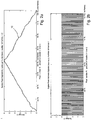
- Fig. 1 shows in a schematic diagram of an example of the voltage characteristic of an analog line of a backplane device according to the prior art.
- the voltage V is shown as the function of the pixel number N for the duration of two frames. Because of the addressing scheme of the prior art, wherein the pixels of a spatial light modulator are addressed line by line and within a single line are addressed one after another, different uniformly distributed voltages between the range of 0 V and 6 V are applied on the analog line of the prior art backplane, whenever the next pixel according to the fixed addressing scheme is addressed. This results in driving analog values from the outside of the display area in a very fast manner, leading to the physical limits of the electronics of a backplane device, for example the large line capacities prevent increasing switching frequencies on the continues analog lines. However, the frame rate or refresh rate of the spatial light modulator can be increased according to the particulars of the present invention.
- a pixel value assigning scheme different to the one known from the prior art is used.
- the diagram in Fig. 2a shows a voltage characteristic 10 being a voltage function which is applied to the analog line of the backplane device, to which the pixels are connected.
- This voltage characteristic 10 shown in the diagram comprises the voltage values which are applied to the analog line during two frames.
- the voltage characteristic 10 comprises the shape of a ramp up function for the first frame and comprises essentially a ramp down function for the second frame.
- the voltage characteristic 10 has been generated depending on the pixel values which have to be assigned to single pixels of the spatial light modulator by the backplane device.
- the voltage characteristic 10 is almost a function comprising a linear increase for the first frame and almost a linear decrease for the second frame, the pixel values to be assigned to the pixels are rather highly distributed. In other words, no regions comprising the same pixel value appear in the two frames which will be assigned by the voltage characteristic 10 of Fig. 2a , because if, for example 1/3 of all pixels would have the same pixel value, this would result in a region of the voltage characteristic 10 being horizontal or parallel to the abscissa as shown in the diagram of Fig. 2a .
- the schematic diagram according to Fig. 2b shows the pixel address signals which are applied to the addressing lines of the backplane device for the first frame. As can be seen, in this embodiment, high frequency signals are applied to the addressing lines. However, because these addressing signals are digital signals having the logical value of either 0 or 1, this can be realized electronically at a higher frequency than realizing the high frequency analog voltage values as they are shown for example in Fig. 1 .
- Fig. 3a shows a part of a spatial light modulator 12 comprising pixels 14.
- the pixels 14 of the spatial light modulator 12 as shown in Fig. 3a comprise four different pixel values 15 being indicated with different hatching. In the example of Fig. 3a four pixels have been assigned with the maximum pixel value 15 of 100%.
- Two pixels 14 comprise the pixel value 15 of 75 %.
- Three pixels 14 comprise the pixel value 15 of 25% and the remaining seven pixels comprise the pixel value 15 of 0%.
- Above the spatial light modulator 12 of Fig. 3a the address numbering of the single pixels in the x-direction is indicated, being from 0 to 3.
- the address numbering of the single pixels 14 in the y-direction are indicated, being 0 to 3.
- Fig. 3b shows in a schematic representation the voltage characteristic 10 to be applied on the analog line (not shown in Fig. 3a, 3b ) for the pixel value 15 distribution as indicated in Fig. 3a .
- the voltage corresponding to the pixel value 15 of 0% is applied to the analog line for a total of 7 pixel addressing cycles.
- the voltage corresponding to the pixel value 15 of 25% is applied to the analog line for three pixel writing cycles.
- the voltage corresponding to a pixel value 15 of 75% is applied for two addressing cycles.
- the voltage corresponding to the pixel value 15 of 100% is assigned for four pixel addressing cycles to complete the assigning of all 16 pixels 14 of the spatial light modulator 12 for one frame as shown in Fig. 3a .
- the voltage characteristic 10 is variable in time and in these examples has predominantly the characteristic a mathematically monotonic function. It is noted, that the voltage characteristic 10 of Fig. 3b is of a continued kind, indicated by the dotted lines between the different voltages indicated by the solid lines.
- the voltage characteristic 10 is generated.
- a ramp up function is applied. Therefore, the voltage characteristics 10 starts with the lowest voltage and increases to the highest voltage. Therefore, the voltage characteristic 10 depends on the pixel values 15 to be assigned to the pixels 14. This is to be understood in particular under the term "pixel value assigning scheme".
- the voltage characteristic 10 is generated by generating means not shown in Fig. 3a and 3b .
- the pixel addresses of the pixels 14 to be addressed when the voltage characteristic 10 is applied to the analog line is determined.
- the pixels 14 comprising a pixel value 15 having 0% need to be addressed first. Therefore, the pixels (0,2), (1,0), (1,1), (1,3), (3,0), (3,1) and (3,3) are generated. It is not necessary that the addresses of the pixels 14 having the 0% pixel value 15 are exactly in the order as indicated above. A different order of assigning these pixel values 15 to the pixels 14 could be used as well. Therefore, it is possible that the generated voltage characteristic 10 being applied to the at least one analog line determines the order of addressing of the pixels 14. In this example, the addressing of all pixels 14 to which the same pixel value 15 is assigned is performed in temporal proximity to each other.
- Fig. 4 shows an example of a backplane device 16 comprising a plurality of clusters 18.
- Fig. 4 does not show the complete backplane device 16, but only a single section of it. Therefore, only four clusters 18 are shown in Fig. 4 .
- Every cluster 18 comprises pixel circuits 20 being indicated schematically with single squares. Every pixel circuit 20 is assigned to pixel of the spatial light modulator 12 (not shown in Fig. 4 ).
- the clusters 18 are controlled independently from each other.
- the pixels and therefore the pixel circuits 20 form a connected and contiguous region of the backplane device 16 as well as of the spatial light modulator to form the cluster 18.
- the connected regions of this embodiment have a rectangular shape and the clusters 18 do not extent over the full width or over the full length of the backplane device 16 or the spatial light modulator.
- Every cluster 18 comprises an analog line 22 as well as pixel addressing means 24 for addressing the pixels or the pixel circuits 20 of the cluster 18. It is schematically indicated in Fig. 4 , that pixel data coming for example for a computer are transferred to the display electronics of the display device in which the spatial light modulator and the backplane device 16 is included. The display electronics transfers the pixel values and the addressing values to the panel electronics of the backplane device 16. Depending on the particular configuration of the display device, the voltage characteristic 10 and the pixel address can be generated either in the computer or in the display electronics of the display device or in the panel electronics of the backplane device 16. In Fig.
- each cluster 18 comprises a connecting line between the panel electronics and the pixel addressing means 24 for transferring address information to the pixel addressing means 24. It is schematically shown in Fig. 4 that the pixel addressing means 24 is connected and/or comprises x-addressing lines 26. The addressing means 24 for addressing the y-address of a pixel comprises y-addressing lines 28.
- Fig. 31 shows in a schematic representation of another example of a small cluster 18.
- the cluster 18 shown in Fig. 31 comprises only 16 pixels and the pixel circuits 20 therefore (of which only 3 pixel circuits 20 are shown in Fig. 31 ), only for the sake of explanation. In reality, clusters will have more pixels, but can be operated in the same way.
- cluster designs are possible. They differ in regard to their number of TFT per pixel and to the number and arrangement of the electrical lines. Different cluster designs usually comprise different features.
- the cluster 18 as shown in Fig. 31 is controlled by an address decoder circuit 50 which comprises an x-address decoder 38 and a y-address decoder 44.
- the x-address decoder 38 and the y-address decoder 44 receive addresses, e.g. x_Addr[1:0] and y_Addr[1:0], from the panel electronics (not shown).
- Each single pixel circuit 20 comprises a TFT circuit composed of 2, 3 or more TFTs.
- a 3-TFT variant according to the example of Fig. 7 is chosen, because it offers additional features.
- the pixel circuit 20 comprises two selection TFTs 100, 200 and a transfer TFT 300. If both selection TFTs 100, 200 are activated, they connect the enable line 22 to the gate of the transfer TFT 300 in order to switch it on or off respectively. When the transfer TFT 300 is switched on, the analogue voltage from the analogue line 22 will be applied to pixel electrode 500.
- each pixel electrode 500 Due to the random access of each pixel electrode 500 by the cluster configuration, it is possible to control that a certain analogue voltage, provided by the panel electronic, is sequentially applied to several pixel cells with arbitrary positions within the cluster 18. Subsequently, the voltage on the analog line 22 is increased and the appropriate pixels are selected to be addressed. Once they are, the voltage being applied on the analog line 22 is applied to a such a pixel electrode 50 or to such a group of pixel electrodes 500.
- the address decoders 50 schematically depicted beside the cluster 18 in Fig. 31 are actually implemented such that they are distributed over the pixel circuits 20 of the entire cluster 18, as shown e.g. in Fig. 12 . This will avoid gaps in between the clusters.
- maximum frame rate of the cluster based approach only depends on the maximum switching frequencies of implemented TFTs 100, 200, 300.
- a ramp-up voltage (the voltage characteristic 10) is applied to the analog line 22 by the panel electronics.
- the ramp-up starts with the lowest voltage, i.e. 0V.
- all transfer TFTs 300 still remain enabled and therefore conductive. This means that changing the voltage V applied on the analog line 22 will change the voltages over all pixel electrodes 500.
- the voltage applied on the analog line 22 is increased to a higher value (for instance to 1V) and this amount is applied to all pixel electrodes 500, except for those that were already disabled in the previously described first step. All pixel electrodes 500 that should store 1V are isolated by individual deactivation operations, comprising to switch the selection TFTs 100, 200 "On” and the enable line 30 "Off'. Then the ramp-up voltage and pixel deactivation continues, until all voltage levels which are to be assigned to the pixels are completed.
- a higher value for instance to 1V
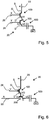
- Figures 5 and 29 show an example of a control circuit 20 (or pixel circuit) for a pixel comprises two TFTs 100, 200 according to the first embodiment mentioned above.
- the source S of the first TFT 100 is connected to the analog line 22, the gate G of the first TFT 100 is connected to an x-addressing line 26 and the drain D of the first TFT 100 is connected to the second TFT 200.
- the source S of the second TFT 200 is connected to the drain D of the first TFT 100, the gate G of the second TFT 200 is connected to a y-addressing line 28 and the drain D of the second TFT 200 is connected to the electrode 500 of the pixel.
- the electrode 500 of the pixel is indicated as a capacitor.
- first TFT 100 is connected to the x-addressing line 26 and the second TFT 200 is connected to the y-addressing line 28, it could also be vice versa, i.e. the first TFT 100 could be connected to the y-addressing line 28 and the second TFT 200 could be connected to the x-addressing line 26 instead.
- the TFTs 100, 200 connected to the x and y address lines 26, 28, respectively have the function of selection TFTs, selecting, if the transfer TFT 300 is switched on or off by controlling the voltage on the gate of the transfer TFT 300.
- the source S of the transfer TFT 300 is connected to the analog line 22 and the drain D is connected to the pixel electrode 500. If this transistor 300 is switched on, the charges are transferred from the analog line 22 to the pixel electrode 500. If the transistor 300 is switched off, the actual charge is stored on the pixel electrode 500 defining the pixel value.
- Fig. 6 shows an example of a control circuit 20 for a pixel comprising two TFTs 100, 200 according to the second embodiment mentioned above.
- the first TFT 100 - a selection TFT - is connected to an x-addressing line 26, to a y-addressing line 28 and to the second TFT 200.
- the second TFT 200 - a transfer TFT - is connected to the first TFT 100, to the analog line 22 and to the electrode 500 of the pixel.
- Such a pixel circuit 20 is comparable to a circuit of a DRAM (Dynamic Random Access Memory) storage cell.
- DRAM Dynamic Random Access Memory
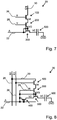
- Fig. 7 shows an example of a control circuit 20 for a pixel comprising three TFTs 100, 200, 300 according to the third embodiment mentioned above.
- the first TFT 100 is connected to the enable line 30, to an x-addressing line 26 and to the second TFT 200.
- the second TFT 200 is connected to the first TFT 100, to a y-addressing line 28 and to the third TFT 300.
- the third TFT 300 - also called transfer TFT - is connected to the second TFT 200, to the analog line 22 and to the electrode 500 of the pixel.
- Fig. 8 shows an example of a control circuit 20 for a pixel comprising four TFTs 100, 200, 300, 400.
- the first TFT 100 is connected to the x-addressing line 26 (X0) of a neighbouring pixel (not shown in Fig. 8 ) - as an enabling function and therefore indicated with reference numeral 30 -, to an x-addressing line 26 and to the second TFT 200.
- the second TFT 200 is connected to the first TFT 100, to a y-addressing line 28 and to the third TFT 300.
- the y-addressing line 28 is generated with the help of the fourth TFT 400 from the analog line 22.
- the third TFT 300 - also called transfer TFT - is connected to the second TFT 200, to the analog line 22 - via the fourth TFT 400 - and to the electrode 500 of the pixel.
- Fig. 9 shows an example of two control circuits 20, 32 for two neighbouring pixels, each control circuit 20 or 32 comprising three TFTs 100, 200, 300 according to the fourth embodiment mentioned above.
- the two pixels are addressed by the same y-addressing line 28.
- the first TFT 100 of the first pixel circuit 20 is connected to the x-addressing line 26 (X1) of the second pixel circuit 32 - as an enabling function and therefore indicated with reference numeral 30 -, to the y-addressing line 28 and to the second TFT 200 of the first pixel circuit 20.
- the second TFT 200 of the first pixel circuit 20 is connected to the first TFT 100 of the first pixel circuit 20, to an x-addressing line 26 (X0) of the first pixel circuit 20 and to the third TFT 300 of the first pixel circuit 20.
- the third TFT 300 of the first pixel circuit 20 is connected to the second TFT 200 of the first pixel circuit 20, to the analog line 22 and to the electrode 500 of the first pixel circuit 20.
- the first TFT 100 of the second pixel circuit 32 is connected to the x-addressing line 26 (X0) of the first pixel circuit 20 - as an enabling function and therefore indicated with reference numeral 30 -, to the y-addressing line 28 and to the second TFT 200 of the second pixel circuit 32.
- the second TFT 200 of the second pixel circuit 32 is connected to the first TFT 100 of the second pixel circuit 32, to an x-addressing line 26 (X1) of the second pixel circuit 32 and to the third TFT 300 of the second pixel circuit 32.
- the third TFT 300 of the second pixel circuit 32 is connected to the second TFT 200 of the second pixel circuit 32, to the analog line 22 and to the electrode 500 of the second pixel circuit 32.
- This embodiment does not have to have a separate enable line on the backplane device for the enablement functionality of a pixel. This is achieved by using the x-addressing line of the one pixel as the enable line for the other pixel of the two neighbouring pixels.
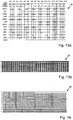
- n-channel-transfer TFT & n-channel-selection TFT Y X1 X0 1 1 1 enable both 1 0 1 disable left 1 1 0 disable right p-channel-transfer TFT & n-channel-selection TFT Y X1 X0 1 1 1 disable both 1 0 1 enable left 1 1 0 enable right p-channel-transfer TFT & p-channel-selection TFT Y X1 X0 1 1 1 disable both 1 0 1 enable left 1 1 0 enable right p-channel-transfer TFT & p-channel-selection TFT Y X1 X0 0 0 enable both 0 1 0 disable left 0 0 1 disable right
- Fig. 10 shows an example of four control circuits 20, 32, 34, 36 for four neighbouring pixels
- each control circuit 20, 32, 34 or 36 comprise three TFTs 100, 200, 300 according to the fifth embodiment mentioned above.
- the four pixels are located adjacent to each other and are addressed by the same y-addressing line 28.
- the first TFT 100 of the first pixel circuit 20 is connected to the x-addressing line 26 (X2) of the third pixel circuit 34 - as an enabling function and therefore indicated with reference numeral 30 -, to the y-addressing line 28 and to the second TFT 200 of the first pixel circuit 20.
- the second TFT 200 of the first pixel circuit 20 is connected to the first TFT 100 of the first pixel circuit 20, to an x-addressing line 26 (X0) of the first pixel circuit 20 and to the third TFT 300 of the first pixel circuit 20.
- the third TFT 300 of the first pixel circuit 20 is connected to the second TFT 200 of the first pixel circuit 20, to the analog line 22 and to the electrode 500 of the first pixel circuit 20.
- the first TFT 100 of the second pixel circuit 32 is connected to the x-addressing line 26 (X0) of the first pixel circuit 20 - as an enabling function and therefore indicated with reference numeral 30 -, to the y-addressing line 28 and to the second TFT 200 of the second pixel circuit 32.
- the second TFT 200 of the second pixel circuit 32 is connected to the first TFT 100 of the second pixel circuit 32, to an x-addressing line 26 (X1) of the second pixel circuit 32 and to the third TFT 300 of the second pixel circuit 32.
- the third TFT 300 of the second pixel circuit 32 is connected to the second TFT 200 of the second pixel circuit 32, to the analog line 22 and to the electrode 500 of the second pixel circuit 32.
- the first TFT 100 of the third pixel circuit 34 is connected to the x-addressing line 26 (X3) of the fourth pixel circuit 36 - as an enabling function and therefore indicated with reference numeral 30 -, to the y-addressing line 28 and to the second TFT 200 of the third pixel circuit 34.
- the second TFT 200 of the third pixel circuit 34 is connected to the first TFT 100 of the third pixel circuit 34, to an x-addressing line 26 (X2) of the third pixel circuit 34 and to the third TFT 300 of the third pixel circuit 34.
- the third TFT 300 of the third pixel circuit 34 is connected to the second TFT 200 of the third pixel circuit 34, to the analog line 22 and to the electrode 500 of the third pixel circuit 34.
- the first TFT 100 of the fourth pixel circuit 36 is connected to the x-addressing line 26 (X1) of the second pixel circuit 32 - as an enabling function and therefore indicated with reference numeral 30 -, to the y-addressing line 28 and to the second TFT 200 of the fourth pixel circuit 36.
- the second TFT 200 of the fourth pixel circuit 36 is connected to the first TFT 100 of the fourth pixel circuit 36, to an x-addressing line 26 (X3) of the fourth pixel circuit 36 and to the third TFT 300 of the fourth pixel circuit 36.
- the third TFT 300 of the fourth pixel circuit 36 is connected to the second TFT 200 of the fourth pixel circuit 36, to the analog line 22 and to the electrode 500 of the fourth pixel circuit 36.
- this embodiment does not have to have a separate enable line on the backplane device for the enablement functionality of a pixel. This can be achieved, if for one pixel, the x-addressing line of one of the other pixels of the four neighbouring pixels is used as the enable line for this pixel.
- Fig. 11 shows an example of an x-address decoder 38 comprising Dynamic-NOR circuits being indicated on the top of the representation of Fig. 11 .
- the x-address decoder 38 can be used for addressing all pixel circuits 20 comprising the two TFTs, which are shown in the bottom of the representation of Fig. 11 .
- the x-address decoder 38 could, for example, be located at the outside edge of the backplane device.
- the pixels circuits 20 as shown in the bottom of Fig. 11 are comparable to the pixels circuits as shown in Fig. 5 .
- Fig. 12 shows an example of an x-address decoder 38 comprising dynamic-NOR circuits for the two TFT pixel circuits 20.
- the x-address decoder 38 is embedded between the pixel circuits 20.
- the y-address decoder (not shown in Fig. 12 ) could also be embedded between the pixel circuits 20.
- Fig. 13a shows a detail of an example of an x-address decoder 38 which comprises dynamic-NOR circuits. This address decoder as shown in Fig. 13a is used for addressing sixteen x-addressing lines, indicated by X0, ..., X15.
- Fig. 13b shows the x-address decoder 38 of Fig. 13a for addressing 64 x-addressing lines.
- This decoder comprises dynamic-NOR circuits being suitable to address three TFT pixel circuits 20.
- Fig. 14 shows an example of an x-address decoder 38 which comprises dynamic-NAND components. These components can be composed from CMOS-elements.
- the x-address decoder 38 as shown in Fig. 15 is suitable for addressing 16 TFTs on the x-addressing lines X0 to X15 and Fig. 16 shows an example of an x-address decoder 38 comprising OR elements.
- Fig. 17 shows an example of a regular arrangement of pixel circuits 20 of the backplane device 16.
- the pixel circuits 20 as shown in Fig. 17 comprise two TFTs 100, 200.
- the pixel control circuits 20 are arranged in a regular layout, i.e. pixel circuits 20 are oriented in same way.
- Fig. 18 shows an example of an arrangement of pixel circuits 20, wherein the pixel circuits 20 of one row 40 is mirrored to the pixel circuits of a second row 42.
- the axis of symmetry or mirror axis is located horizontally between the two rows 40, 42.
- the arrangement of pixel circuits according to Fig. 18 comprises the x-address decoder 38 and y-address decoder 44 between the pixel circuits 20 on the backplane device 16 itself.
- the first row 40' is the mirror image of the second row 42', wherein the axis of symmetry is located horizontally between the two rows 40', 42'.
- row 40 is the mirror image of another row 40', wherein the axis of symmetry for such a mirroring axis is located in a vertical direction. The same is true with a row 42 and 42'.
- Fig. 19 shows an example of an arrangement of pixel circuits 20 being mirrored in two directions of the backplane device 16 as can be seen for example with the four pixel circuits 20 being located on the right hand side and at the top of Fig. 19 .
- the pixel circuits 20 of the right most columns is the mirror image of the column of pixel circuits being located with the left, wherein the mirror axis can be regarded as for example the analog line 22.
- the top row 40 can be regarded as the mirror image of the row 42 being located next to the top row 40.
- the mirror axis or axis of symmetry can be regarded as a horizontal line between row 40 and row 42.
- the pixels circuits 20 as shown in Fig. 19 are comparable to the pixel circuits 20 of Figs. 17 and/or 18, except for their orientation.
- the rectangles 46 as shown in Fig. 19 indicate possible locations of address decoders for the pixel circuits 20, the address decoder circuits are not shown in Fig. 19 .
- Fig. 20 shows in a schematic diagram an example for an adaptive overdrive being possible with the value sorted addressing approach according to the present invention.
- pixel electrodes 500 can remain connected to the analogue line 22 for much longer periods of the total frame time.
- the overdrive values can be applied for a long, medium or short period of time, depending on the desired pixel value to be assigned to a pixel.
- the pixel voltage is much closer to the exact voltage (representing the pixel value) needed to switch the LC (Liquid Crystals) molecules of a spatial light modulator to the desired pixel value than it would be in a standard overdrive scheme.
- an overdrive voltage being higher than the voltage normally used to switch a pixel fully on.
- Fig. 20 shows an overdrive pulse 48 with a value of 12V as it is "seen” by the LC molecules of the pixels with a normal maximal pixel voltage of 6V (see time period between enable and disable marked by the arrows below the diagram).
- An overdrive pulse e.g. 48', 48" is applied for a shorter time period to pixels to which a lower phase and voltage pixel value needs to be assigned, respectively.
- the time to achieve a LC molecules rotation corresponding to a static voltage of 4V is very short, if a 12V overdrive voltage is used.
- On the right side of Fig. 20 one can see the overdrive time and effect of the overdrive that is actually applied to a pixel.
- This operation mode of the method according to the invention significantly speeds up grey-to-grey switching in the on-direction.
- the frame time can be regarded as the sum of tOFF (being the time it takes for the LC molecules to get in the 0V or in a predetermined position) and the time the backlight is switched on (tBL), provided tOFF is at least the time to write in all pixel values (tWR).
- tOFF being the time it takes for the LC molecules to get in the 0V or in a predetermined position
- tWR the time the backlight is switched on
- the maximum worse case frame time is either the sum of tOFF + tBL or tWR + tON + tBL, depending on which time is longer.
- tON is the time it takes for the LC molecules to get in the position/orientation determined by the electrical field being generated by the electrode of a pixel. For a conventional display with a flashing backlight, this time is much longer and a minimum tWR + tOFF + tBL. Even for a conventional display with a scanning backlight, the frame time is at least tOFF + tBL. If tON is longer than tOFF, a pre-charge to maximum can be combined with a ramp-up cycle analog to the described solution.
- the LC molecule response time can be further increased by writing additional overdrive values into the pixel. This could be applied to, for instance, 10% of the "slowest" pixels only. This overdrive can be achieved by clever sorting of the pixel values.
- the value sorted approach can achieve the same frame time using only a flashing backlight as a conventional display with a more costly scanning backlight. This is essential for display types like holographic displays, which might not allow a scanning backlight. But this solution can also reduce costs for normal LC displays. For holographic displays, the frame time can be even further reduced by putting the write time (tWR) into the tOFF time.
- the advantageous for LC switching times to be obtained by operation modes like underdrive and overdrive are described.
- the LC switching time effect only the motion blur but for 3D and holographic displays using time sequential separation of different views, the LC switching time defines the useable frame rate.
- This frame rate should be e.g. at least 2x50Hz for a flicker free image for one user.
- Standard AM displays re-write values (or assign new pixel values to pixels) only once per frame. So in fact, the possibilities to apply an overdrive are limited. It is not possible to apply a higher voltage for a shorter or a longer time because the time period is fixed and determined by the frame rate.
- Fig. 21 and 22 show an LC switching from 5V to 3V for a conventional AM display without an initialization to 0V. This display exhibits a slow gray to gray switching time, which is longer than in the proposed new driving scheme shown e.g. in Fig. 23 and even longer than tOFF.
- Fig. 21 shows the situation for an arbitrary line of a display with a scanning backlight or for the first line of a display with flashing backlight.
- Fig. 22 shows the relations for the last line of a display with a flashing backlight, which is even worse, because the LC molecules are not yet oriented as they should be, see the large difference between the dotted line (representing the orientation status of LC molecules) and the 3V orientation value.
- the value sorted approach allows to apply multiple values per frame.
- the value sorted approach can speed up the LC switching by applying initial values and also use LC switching times better than any other driving method.
- the explanation assumes a spatial light modulator or a LC display with an LC-mode that is ON at 6V and OFF at 0V.
- the rotation of the LC into the direction driven by the electrical field (tON) can be speed-up by applying a higher voltage.
- tON electrical field
- the special overdrive scheme can be used to speed up the switching in the on direction.
- this implementation of the values-sorted approach drives all pixels to 0V value immediately after frame start, so the LC of all pixels starts turning to the off direction with maximum (passive) relaxation force.
- the address mode is changed to access only single pixels, but the pixel electrodes remain 0V until the pixel is accessed again.
- Fig. 24 shows the update from an old pixel value of 2V to a new pixel value of 5V.
- the initialisation to 0V at frame start assigns the LC molecules for this pixel to start to rotate in the wrong direction, however, this rotation by the passive relaxation is relatively slow.
- the LC rotates back in the correct direction at even higher forces and faster times.
- the higher the possible rotation angle into the on-direction the earlier the pixel is addressed, therefore minimizing the effect of a possible rotation in the wrong direction and enlarging the time from the write in of the pixel value to switching on the backlight.
Landscapes
- Physics & Mathematics (AREA)
- Engineering & Computer Science (AREA)
- General Physics & Mathematics (AREA)
- Computer Hardware Design (AREA)
- Theoretical Computer Science (AREA)
- Optics & Photonics (AREA)
- Control Of Indicators Other Than Cathode Ray Tubes (AREA)
- Liquid Crystal (AREA)
- Liquid Crystal Display Device Control (AREA)
- Devices For Indicating Variable Information By Combining Individual Elements (AREA)
- Holo Graphy (AREA)
Priority Applications (1)
| Application Number | Priority Date | Filing Date | Title |
|---|---|---|---|
| EP11708461.6A EP2548194B1 (en) | 2010-03-15 | 2011-03-15 | Backplane device for a spatial light modulator and method for operating a backplane device |
Applications Claiming Priority (3)
| Application Number | Priority Date | Filing Date | Title |
|---|---|---|---|
| EP10156572 | 2010-03-15 | ||
| EP11708461.6A EP2548194B1 (en) | 2010-03-15 | 2011-03-15 | Backplane device for a spatial light modulator and method for operating a backplane device |
| PCT/EP2011/053912 WO2011113843A1 (en) | 2010-03-15 | 2011-03-15 | Backplane device for a spatial light modulator and method for operating a backplane device |
Publications (2)
| Publication Number | Publication Date |
|---|---|
| EP2548194A1 EP2548194A1 (en) | 2013-01-23 |
| EP2548194B1 true EP2548194B1 (en) | 2021-09-01 |
Family
ID=43903938
Family Applications (1)
| Application Number | Title | Priority Date | Filing Date |
|---|---|---|---|
| EP11708461.6A Active EP2548194B1 (en) | 2010-03-15 | 2011-03-15 | Backplane device for a spatial light modulator and method for operating a backplane device |
Country Status (8)
| Country | Link |
|---|---|
| US (1) | US9076375B2 (https=) |
| EP (1) | EP2548194B1 (https=) |
| JP (1) | JP5907899B2 (https=) |
| KR (1) | KR101819073B1 (https=) |
| CN (1) | CN103038808B (https=) |
| CA (1) | CA2793123C (https=) |
| TW (1) | TWI507733B (https=) |
| WO (1) | WO2011113843A1 (https=) |
Families Citing this family (9)
| Publication number | Priority date | Publication date | Assignee | Title |
|---|---|---|---|---|
| WO2012028678A2 (en) | 2010-09-01 | 2012-03-08 | Seereal Technologies S.A. | Backplane device |
| JPWO2015040971A1 (ja) | 2013-09-18 | 2017-03-02 | 株式会社Jvcケンウッド | 画像表示装置 |
| KR20150066901A (ko) | 2013-12-09 | 2015-06-17 | 삼성전자주식회사 | 디스플레이 패널의 구동 장치 및 구동 방법 |
| KR102536628B1 (ko) * | 2015-08-24 | 2023-05-26 | 엘지디스플레이 주식회사 | 투명표시장치 |
| US20210223738A1 (en) * | 2015-12-28 | 2021-07-22 | Seereal Technologies S.A. | Display device and method for optimizing the image quality |
| US11716548B2 (en) | 2018-03-13 | 2023-08-01 | Meta Platforms Technologies, Llc | Timing of multiplexed sensor phase measurements in a depth camera assembly for depth determination using fringe interferometry |
| US10665319B1 (en) * | 2018-09-20 | 2020-05-26 | Amazon Technologies, Inc. | Memory device testing |
| CN115346498B (zh) * | 2021-05-14 | 2026-01-20 | 深圳晶微峰光电科技有限公司 | 一种硅基液晶面板及其像素电路 |
| CN116170547B (zh) * | 2023-02-16 | 2026-02-03 | 上海瑞立柯信息技术有限公司 | 一种空间光调制器控制方法、空间光调制器及控制系统 |
Family Cites Families (29)
| Publication number | Priority date | Publication date | Assignee | Title |
|---|---|---|---|---|
| JPH0683416B2 (ja) * | 1986-10-24 | 1994-10-19 | 株式会社日立製作所 | 液晶表示装置用駆動回路 |
| JP3295953B2 (ja) * | 1991-11-11 | 2002-06-24 | セイコーエプソン株式会社 | 液晶表示体駆動装置 |
| JPH0667154A (ja) * | 1992-08-14 | 1994-03-11 | Semiconductor Energy Lab Co Ltd | 液晶電気光学装置の駆動方法 |
| JP3070893B2 (ja) * | 1993-08-26 | 2000-07-31 | シャープ株式会社 | 液晶駆動装置 |
| JPH07319429A (ja) * | 1994-05-30 | 1995-12-08 | Matsushita Electric Ind Co Ltd | 液晶画像表示装置の駆動方法および液晶画像表示装置 |
| JPH07334124A (ja) * | 1994-06-08 | 1995-12-22 | Casio Comput Co Ltd | 液晶駆動装置 |
| JP3234131B2 (ja) * | 1995-06-23 | 2001-12-04 | 株式会社東芝 | 液晶表示装置 |
| US6329973B1 (en) * | 1995-09-20 | 2001-12-11 | Hitachi, Ltd. | Image display device |
| US20030071813A1 (en) * | 1996-06-05 | 2003-04-17 | Alessandro Chiabrera | Three-dimensional display system: apparatus and method |
| JP3947249B2 (ja) * | 1996-07-10 | 2007-07-18 | 株式会社日立製作所 | 画像表示素子、画像表示装置およびその駆動方法 |
| KR20030010607A (ko) * | 2000-04-26 | 2003-02-05 | 울트라칩, 인코포레이티드. | 저전력 엘씨디 구동 방식 |
| JP3705086B2 (ja) * | 2000-07-03 | 2005-10-12 | 株式会社日立製作所 | 液晶表示装置 |
| JP3428593B2 (ja) | 2000-09-05 | 2003-07-22 | 株式会社東芝 | 表示装置及びその駆動方法 |
| JP2003050404A (ja) * | 2001-08-06 | 2003-02-21 | Hitachi Ltd | アクティブマトリクス型液晶表示装置 |
| SG120888A1 (en) * | 2001-09-28 | 2006-04-26 | Semiconductor Energy Lab | A light emitting device and electronic apparatus using the same |
| US7492513B2 (en) * | 2002-01-23 | 2009-02-17 | Sergey Fridman | Autostereoscopic display and method |
| EP1414011A1 (en) * | 2002-10-22 | 2004-04-28 | STMicroelectronics S.r.l. | Method for scanning sequence selection for displays |
| JP2006030592A (ja) * | 2004-07-16 | 2006-02-02 | Ricoh Co Ltd | 画像表示装置及びその駆動回路 |
| DE102004063838A1 (de) | 2004-12-23 | 2006-07-06 | Seereal Technologies Gmbh | Verfahren und Einrichtung zum Berechnen computer generierter Videohologramme |
| TW200638304A (en) * | 2005-04-22 | 2006-11-01 | Silicon Touch Tech Inc | Driving method and device enabling a display to reduce power consumption |
| US20070263016A1 (en) * | 2005-05-25 | 2007-11-15 | Naugler W E Jr | Digital drive architecture for flat panel displays |
| US7605785B2 (en) * | 2005-07-12 | 2009-10-20 | Eastman Kodak Company | Black level uniformity correction method |
| JP2007047348A (ja) * | 2005-08-09 | 2007-02-22 | Sanyo Epson Imaging Devices Corp | 電気光学装置、駆動方法および電子機器 |
| JP4790798B2 (ja) * | 2006-05-19 | 2011-10-12 | シャープ株式会社 | アクティブマトリクス型液晶表示装置及びその駆動方法 |
| GB2482076B (en) | 2007-05-16 | 2012-08-22 | Seereal Technologies Sa | Communications system including a holographic display |
| GB0718626D0 (en) | 2007-05-16 | 2007-11-07 | Seereal Technologies Sa | Holograms |
| DE102007040712B4 (de) | 2007-08-23 | 2014-09-04 | Seereal Technologies S.A. | Elektronisches Anzeigegerät und Vorrichtung zur Ansteuerung von Pixeln eines Displays |
| TWI428875B (zh) | 2008-01-21 | 2014-03-01 | Seereal Technologies Sa | An apparatus for controlling the pixels of the pixel array |
| CA3062343A1 (en) | 2009-06-23 | 2010-12-29 | Seereal Technologies S.A. | Light modulator device used for a display for the presentation of two- and/or three-dimensional image contents |
-
2011
- 2011-03-15 TW TW100108865A patent/TWI507733B/zh active
- 2011-03-15 WO PCT/EP2011/053912 patent/WO2011113843A1/en not_active Ceased
- 2011-03-15 US US13/635,104 patent/US9076375B2/en active Active
- 2011-03-15 CA CA2793123A patent/CA2793123C/en active Active
- 2011-03-15 EP EP11708461.6A patent/EP2548194B1/en active Active
- 2011-03-15 CN CN201180024060.1A patent/CN103038808B/zh active Active
- 2011-03-15 JP JP2012557532A patent/JP5907899B2/ja active Active
- 2011-03-15 KR KR1020127026915A patent/KR101819073B1/ko active Active
Also Published As
| Publication number | Publication date |
|---|---|
| US20130002638A1 (en) | 2013-01-03 |
| US9076375B2 (en) | 2015-07-07 |
| KR20130018772A (ko) | 2013-02-25 |
| JP2013525825A (ja) | 2013-06-20 |
| TW201213859A (en) | 2012-04-01 |
| CN103038808B (zh) | 2016-08-03 |
| CN103038808A (zh) | 2013-04-10 |
| WO2011113843A1 (en) | 2011-09-22 |
| CA2793123C (en) | 2018-08-28 |
| CA2793123A1 (en) | 2011-09-22 |
| EP2548194A1 (en) | 2013-01-23 |
| KR101819073B1 (ko) | 2018-01-16 |
| JP5907899B2 (ja) | 2016-04-26 |
| TWI507733B (zh) | 2015-11-11 |
Similar Documents
| Publication | Publication Date | Title |
|---|---|---|
| EP2548194B1 (en) | Backplane device for a spatial light modulator and method for operating a backplane device | |
| KR102730170B1 (ko) | 액정 표시 장치 | |
| US7230597B2 (en) | Active matrix array devices | |
| US9860943B2 (en) | Backplane device | |
| JP2010511900A (ja) | 低消費電力アクティブ・マトリックス・ディスプレイ | |
| US7061463B2 (en) | Addressing technique for an active backplane device | |
| JP2002533768A5 (https=) | ||
| MX2011010906A (es) | Pantalla de matriz activa de energia baja. | |
| US20090244419A1 (en) | Liquid crystal display device | |
| CN101297344B (zh) | 用于显示设备的复位电路 | |
| WO2012023467A1 (ja) | 表示装置 | |
| CN111399303B (zh) | 电光显示器 | |
| KR20080032248A (ko) | 액정 디스플레이 디바이스를 위한 능동 매트릭스 | |
| KR100879769B1 (ko) | 능동 매트릭스 어레이 장치 | |
| WO2023081119A1 (en) | Methods for driving electro-optic displays | |
| HK40026776B (en) | Electro-optic displays |
Legal Events
| Date | Code | Title | Description |
|---|---|---|---|
| PUAI | Public reference made under article 153(3) epc to a published international application that has entered the european phase |
Free format text: ORIGINAL CODE: 0009012 |
|
| 17P | Request for examination filed |
Effective date: 20121015 |
|
| AK | Designated contracting states |
Kind code of ref document: A1 Designated state(s): AL AT BE BG CH CY CZ DE DK EE ES FI FR GB GR HR HU IE IS IT LI LT LU LV MC MK MT NL NO PL PT RO RS SE SI SK SM TR |
|
| DAX | Request for extension of the european patent (deleted) | ||
| RAP1 | Party data changed (applicant data changed or rights of an application transferred) |
Owner name: SEEREAL TECHNOLOGIES S.A. |
|
| RAP1 | Party data changed (applicant data changed or rights of an application transferred) |
Owner name: SEEREAL TECHNOLOGIES S.A. |
|
| STAA | Information on the status of an ep patent application or granted ep patent |
Free format text: STATUS: EXAMINATION IS IN PROGRESS |
|
| 17Q | First examination report despatched |
Effective date: 20171213 |
|
| GRAP | Despatch of communication of intention to grant a patent |
Free format text: ORIGINAL CODE: EPIDOSNIGR1 |
|
| STAA | Information on the status of an ep patent application or granted ep patent |
Free format text: STATUS: GRANT OF PATENT IS INTENDED |
|
| RIC1 | Information provided on ipc code assigned before grant |
Ipc: G03H 1/04 20060101ALI20201028BHEP Ipc: G09G 3/20 20060101AFI20201028BHEP |
|
| INTG | Intention to grant announced |
Effective date: 20201127 |
|
| GRAS | Grant fee paid |
Free format text: ORIGINAL CODE: EPIDOSNIGR3 |
|
| GRAJ | Information related to disapproval of communication of intention to grant by the applicant or resumption of examination proceedings by the epo deleted |
Free format text: ORIGINAL CODE: EPIDOSDIGR1 |
|
| GRAL | Information related to payment of fee for publishing/printing deleted |
Free format text: ORIGINAL CODE: EPIDOSDIGR3 |
|
| STAA | Information on the status of an ep patent application or granted ep patent |
Free format text: STATUS: EXAMINATION IS IN PROGRESS |
|
| GRAP | Despatch of communication of intention to grant a patent |
Free format text: ORIGINAL CODE: EPIDOSNIGR1 |
|
| STAA | Information on the status of an ep patent application or granted ep patent |
Free format text: STATUS: GRANT OF PATENT IS INTENDED |
|
| INTC | Intention to grant announced (deleted) | ||
| INTG | Intention to grant announced |
Effective date: 20210430 |
|
| GRAA | (expected) grant |
Free format text: ORIGINAL CODE: 0009210 |
|
| STAA | Information on the status of an ep patent application or granted ep patent |
Free format text: STATUS: THE PATENT HAS BEEN GRANTED |
|
| AK | Designated contracting states |
Kind code of ref document: B1 Designated state(s): AL AT BE BG CH CY CZ DE DK EE ES FI FR GB GR HR HU IE IS IT LI LT LU LV MC MK MT NL NO PL PT RO RS SE SI SK SM TR |
|
| REG | Reference to a national code |
Ref country code: GB Ref legal event code: FG4D |
|
| REG | Reference to a national code |
Ref country code: CH Ref legal event code: EP Ref country code: AT Ref legal event code: REF Ref document number: 1427046 Country of ref document: AT Kind code of ref document: T Effective date: 20210915 |
|
| REG | Reference to a national code |
Ref country code: DE Ref legal event code: R096 Ref document number: 602011071680 Country of ref document: DE |
|
| REG | Reference to a national code |
Ref country code: IE Ref legal event code: FG4D |
|
| REG | Reference to a national code |
Ref country code: LT Ref legal event code: MG9D |
|
| REG | Reference to a national code |
Ref country code: NL Ref legal event code: MP Effective date: 20210901 |
|
| PG25 | Lapsed in a contracting state [announced via postgrant information from national office to epo] |
Ref country code: RS Free format text: LAPSE BECAUSE OF FAILURE TO SUBMIT A TRANSLATION OF THE DESCRIPTION OR TO PAY THE FEE WITHIN THE PRESCRIBED TIME-LIMIT Effective date: 20210901 Ref country code: NO Free format text: LAPSE BECAUSE OF FAILURE TO SUBMIT A TRANSLATION OF THE DESCRIPTION OR TO PAY THE FEE WITHIN THE PRESCRIBED TIME-LIMIT Effective date: 20211201 Ref country code: FI Free format text: LAPSE BECAUSE OF FAILURE TO SUBMIT A TRANSLATION OF THE DESCRIPTION OR TO PAY THE FEE WITHIN THE PRESCRIBED TIME-LIMIT Effective date: 20210901 Ref country code: ES Free format text: LAPSE BECAUSE OF FAILURE TO SUBMIT A TRANSLATION OF THE DESCRIPTION OR TO PAY THE FEE WITHIN THE PRESCRIBED TIME-LIMIT Effective date: 20210901 Ref country code: BG Free format text: LAPSE BECAUSE OF FAILURE TO SUBMIT A TRANSLATION OF THE DESCRIPTION OR TO PAY THE FEE WITHIN THE PRESCRIBED TIME-LIMIT Effective date: 20211201 Ref country code: LT Free format text: LAPSE BECAUSE OF FAILURE TO SUBMIT A TRANSLATION OF THE DESCRIPTION OR TO PAY THE FEE WITHIN THE PRESCRIBED TIME-LIMIT Effective date: 20210901 Ref country code: SE Free format text: LAPSE BECAUSE OF FAILURE TO SUBMIT A TRANSLATION OF THE DESCRIPTION OR TO PAY THE FEE WITHIN THE PRESCRIBED TIME-LIMIT Effective date: 20210901 Ref country code: HR Free format text: LAPSE BECAUSE OF FAILURE TO SUBMIT A TRANSLATION OF THE DESCRIPTION OR TO PAY THE FEE WITHIN THE PRESCRIBED TIME-LIMIT Effective date: 20210901 |
|
| REG | Reference to a national code |
Ref country code: AT Ref legal event code: MK05 Ref document number: 1427046 Country of ref document: AT Kind code of ref document: T Effective date: 20210901 |
|
| PG25 | Lapsed in a contracting state [announced via postgrant information from national office to epo] |
Ref country code: PL Free format text: LAPSE BECAUSE OF FAILURE TO SUBMIT A TRANSLATION OF THE DESCRIPTION OR TO PAY THE FEE WITHIN THE PRESCRIBED TIME-LIMIT Effective date: 20210901 Ref country code: LV Free format text: LAPSE BECAUSE OF FAILURE TO SUBMIT A TRANSLATION OF THE DESCRIPTION OR TO PAY THE FEE WITHIN THE PRESCRIBED TIME-LIMIT Effective date: 20210901 Ref country code: GR Free format text: LAPSE BECAUSE OF FAILURE TO SUBMIT A TRANSLATION OF THE DESCRIPTION OR TO PAY THE FEE WITHIN THE PRESCRIBED TIME-LIMIT Effective date: 20211202 |
|
| PG25 | Lapsed in a contracting state [announced via postgrant information from national office to epo] |
Ref country code: AT Free format text: LAPSE BECAUSE OF FAILURE TO SUBMIT A TRANSLATION OF THE DESCRIPTION OR TO PAY THE FEE WITHIN THE PRESCRIBED TIME-LIMIT Effective date: 20210901 |
|
| PG25 | Lapsed in a contracting state [announced via postgrant information from national office to epo] |
Ref country code: IS Free format text: LAPSE BECAUSE OF FAILURE TO SUBMIT A TRANSLATION OF THE DESCRIPTION OR TO PAY THE FEE WITHIN THE PRESCRIBED TIME-LIMIT Effective date: 20220101 Ref country code: SM Free format text: LAPSE BECAUSE OF FAILURE TO SUBMIT A TRANSLATION OF THE DESCRIPTION OR TO PAY THE FEE WITHIN THE PRESCRIBED TIME-LIMIT Effective date: 20210901 Ref country code: SK Free format text: LAPSE BECAUSE OF FAILURE TO SUBMIT A TRANSLATION OF THE DESCRIPTION OR TO PAY THE FEE WITHIN THE PRESCRIBED TIME-LIMIT Effective date: 20210901 Ref country code: RO Free format text: LAPSE BECAUSE OF FAILURE TO SUBMIT A TRANSLATION OF THE DESCRIPTION OR TO PAY THE FEE WITHIN THE PRESCRIBED TIME-LIMIT Effective date: 20210901 Ref country code: PT Free format text: LAPSE BECAUSE OF FAILURE TO SUBMIT A TRANSLATION OF THE DESCRIPTION OR TO PAY THE FEE WITHIN THE PRESCRIBED TIME-LIMIT Effective date: 20220103 Ref country code: NL Free format text: LAPSE BECAUSE OF FAILURE TO SUBMIT A TRANSLATION OF THE DESCRIPTION OR TO PAY THE FEE WITHIN THE PRESCRIBED TIME-LIMIT Effective date: 20210901 Ref country code: EE Free format text: LAPSE BECAUSE OF FAILURE TO SUBMIT A TRANSLATION OF THE DESCRIPTION OR TO PAY THE FEE WITHIN THE PRESCRIBED TIME-LIMIT Effective date: 20210901 Ref country code: CZ Free format text: LAPSE BECAUSE OF FAILURE TO SUBMIT A TRANSLATION OF THE DESCRIPTION OR TO PAY THE FEE WITHIN THE PRESCRIBED TIME-LIMIT Effective date: 20210901 Ref country code: AL Free format text: LAPSE BECAUSE OF FAILURE TO SUBMIT A TRANSLATION OF THE DESCRIPTION OR TO PAY THE FEE WITHIN THE PRESCRIBED TIME-LIMIT Effective date: 20210901 |
|
| REG | Reference to a national code |
Ref country code: DE Ref legal event code: R097 Ref document number: 602011071680 Country of ref document: DE |
|
| PLBE | No opposition filed within time limit |
Free format text: ORIGINAL CODE: 0009261 |
|
| STAA | Information on the status of an ep patent application or granted ep patent |
Free format text: STATUS: NO OPPOSITION FILED WITHIN TIME LIMIT |
|
| PG25 | Lapsed in a contracting state [announced via postgrant information from national office to epo] |
Ref country code: IT Free format text: LAPSE BECAUSE OF FAILURE TO SUBMIT A TRANSLATION OF THE DESCRIPTION OR TO PAY THE FEE WITHIN THE PRESCRIBED TIME-LIMIT Effective date: 20210901 Ref country code: DK Free format text: LAPSE BECAUSE OF FAILURE TO SUBMIT A TRANSLATION OF THE DESCRIPTION OR TO PAY THE FEE WITHIN THE PRESCRIBED TIME-LIMIT Effective date: 20210901 |
|
| 26N | No opposition filed |
Effective date: 20220602 |
|
| PG25 | Lapsed in a contracting state [announced via postgrant information from national office to epo] |
Ref country code: SI Free format text: LAPSE BECAUSE OF FAILURE TO SUBMIT A TRANSLATION OF THE DESCRIPTION OR TO PAY THE FEE WITHIN THE PRESCRIBED TIME-LIMIT Effective date: 20210901 |
|
| PG25 | Lapsed in a contracting state [announced via postgrant information from national office to epo] |
Ref country code: MC Free format text: LAPSE BECAUSE OF FAILURE TO SUBMIT A TRANSLATION OF THE DESCRIPTION OR TO PAY THE FEE WITHIN THE PRESCRIBED TIME-LIMIT Effective date: 20210901 |
|
| REG | Reference to a national code |
Ref country code: CH Ref legal event code: PL |
|
| REG | Reference to a national code |
Ref country code: BE Ref legal event code: MM Effective date: 20220331 |
|
| PG25 | Lapsed in a contracting state [announced via postgrant information from national office to epo] |
Ref country code: LU Free format text: LAPSE BECAUSE OF NON-PAYMENT OF DUE FEES Effective date: 20220315 Ref country code: LI Free format text: LAPSE BECAUSE OF NON-PAYMENT OF DUE FEES Effective date: 20220331 Ref country code: IE Free format text: LAPSE BECAUSE OF NON-PAYMENT OF DUE FEES Effective date: 20220315 Ref country code: CH Free format text: LAPSE BECAUSE OF NON-PAYMENT OF DUE FEES Effective date: 20220331 |
|
| PG25 | Lapsed in a contracting state [announced via postgrant information from national office to epo] |
Ref country code: BE Free format text: LAPSE BECAUSE OF NON-PAYMENT OF DUE FEES Effective date: 20220331 |
|
| P01 | Opt-out of the competence of the unified patent court (upc) registered |
Effective date: 20230529 |
|
| PG25 | Lapsed in a contracting state [announced via postgrant information from national office to epo] |
Ref country code: HU Free format text: LAPSE BECAUSE OF FAILURE TO SUBMIT A TRANSLATION OF THE DESCRIPTION OR TO PAY THE FEE WITHIN THE PRESCRIBED TIME-LIMIT; INVALID AB INITIO Effective date: 20110315 |
|
| PG25 | Lapsed in a contracting state [announced via postgrant information from national office to epo] |
Ref country code: MK Free format text: LAPSE BECAUSE OF FAILURE TO SUBMIT A TRANSLATION OF THE DESCRIPTION OR TO PAY THE FEE WITHIN THE PRESCRIBED TIME-LIMIT Effective date: 20210901 Ref country code: CY Free format text: LAPSE BECAUSE OF FAILURE TO SUBMIT A TRANSLATION OF THE DESCRIPTION OR TO PAY THE FEE WITHIN THE PRESCRIBED TIME-LIMIT Effective date: 20210901 |
|
| PG25 | Lapsed in a contracting state [announced via postgrant information from national office to epo] |
Ref country code: TR Free format text: LAPSE BECAUSE OF FAILURE TO SUBMIT A TRANSLATION OF THE DESCRIPTION OR TO PAY THE FEE WITHIN THE PRESCRIBED TIME-LIMIT Effective date: 20210901 |
|
| PG25 | Lapsed in a contracting state [announced via postgrant information from national office to epo] |
Ref country code: MT Free format text: LAPSE BECAUSE OF FAILURE TO SUBMIT A TRANSLATION OF THE DESCRIPTION OR TO PAY THE FEE WITHIN THE PRESCRIBED TIME-LIMIT Effective date: 20210901 |
|
| PGFP | Annual fee paid to national office [announced via postgrant information from national office to epo] |
Ref country code: DE Payment date: 20250919 Year of fee payment: 15 |
|
| PGFP | Annual fee paid to national office [announced via postgrant information from national office to epo] |
Ref country code: GB Payment date: 20250916 Year of fee payment: 15 |
|
| PGFP | Annual fee paid to national office [announced via postgrant information from national office to epo] |
Ref country code: FR Payment date: 20250924 Year of fee payment: 15 |