EP2530718B1 - Siliciumcarbidhalbleiterbauelement und herstellungsverfahren dafür - Google Patents
Siliciumcarbidhalbleiterbauelement und herstellungsverfahren dafür Download PDFInfo
- Publication number
- EP2530718B1 EP2530718B1 EP10830926.1A EP10830926A EP2530718B1 EP 2530718 B1 EP2530718 B1 EP 2530718B1 EP 10830926 A EP10830926 A EP 10830926A EP 2530718 B1 EP2530718 B1 EP 2530718B1
- Authority
- EP
- European Patent Office
- Prior art keywords
- trench
- silicon carbide
- sidewall
- conductive
- semiconductor layer
- Prior art date
- Legal status (The legal status is an assumption and is not a legal conclusion. Google has not performed a legal analysis and makes no representation as to the accuracy of the status listed.)
- Active
Links
Images


Classifications
-
- H—ELECTRICITY
- H10—SEMICONDUCTOR DEVICES; ELECTRIC SOLID-STATE DEVICES NOT OTHERWISE PROVIDED FOR
- H10D—INORGANIC ELECTRIC SEMICONDUCTOR DEVICES
- H10D12/00—Bipolar devices controlled by the field effect, e.g. insulated-gate bipolar transistors [IGBT]
- H10D12/01—Manufacture or treatment
- H10D12/031—Manufacture or treatment of IGBTs
-
- H—ELECTRICITY
- H10—SEMICONDUCTOR DEVICES; ELECTRIC SOLID-STATE DEVICES NOT OTHERWISE PROVIDED FOR
- H10D—INORGANIC ELECTRIC SEMICONDUCTOR DEVICES
- H10D30/00—Field-effect transistors [FET]
- H10D30/01—Manufacture or treatment
- H10D30/021—Manufacture or treatment of FETs having insulated gates [IGFET]
- H10D30/028—Manufacture or treatment of FETs having insulated gates [IGFET] of double-diffused metal oxide semiconductor [DMOS] FETs
- H10D30/0291—Manufacture or treatment of FETs having insulated gates [IGFET] of double-diffused metal oxide semiconductor [DMOS] FETs of vertical DMOS [VDMOS] FETs
- H10D30/0297—Manufacture or treatment of FETs having insulated gates [IGFET] of double-diffused metal oxide semiconductor [DMOS] FETs of vertical DMOS [VDMOS] FETs using recessing of the gate electrodes, e.g. to form trench gate electrodes
-
- H—ELECTRICITY
- H10—SEMICONDUCTOR DEVICES; ELECTRIC SOLID-STATE DEVICES NOT OTHERWISE PROVIDED FOR
- H10D—INORGANIC ELECTRIC SEMICONDUCTOR DEVICES
- H10D30/00—Field-effect transistors [FET]
- H10D30/60—Insulated-gate field-effect transistors [IGFET]
- H10D30/64—Double-diffused metal-oxide semiconductor [DMOS] FETs
- H10D30/66—Vertical DMOS [VDMOS] FETs
- H10D30/668—Vertical DMOS [VDMOS] FETs having trench gate electrodes, e.g. UMOS transistors
-
- H—ELECTRICITY
- H10—SEMICONDUCTOR DEVICES; ELECTRIC SOLID-STATE DEVICES NOT OTHERWISE PROVIDED FOR
- H10D—INORGANIC ELECTRIC SEMICONDUCTOR DEVICES
- H10D62/00—Semiconductor bodies, or regions thereof, of devices having potential barriers
- H10D62/40—Crystalline structures
- H10D62/405—Orientations of crystalline planes
-
- H—ELECTRICITY
- H10—SEMICONDUCTOR DEVICES; ELECTRIC SOLID-STATE DEVICES NOT OTHERWISE PROVIDED FOR
- H10D—INORGANIC ELECTRIC SEMICONDUCTOR DEVICES
- H10D62/00—Semiconductor bodies, or regions thereof, of devices having potential barriers
- H10D62/80—Semiconductor bodies, or regions thereof, of devices having potential barriers characterised by the materials
- H10D62/83—Semiconductor bodies, or regions thereof, of devices having potential barriers characterised by the materials being Group IV materials, e.g. B-doped Si or undoped Ge
- H10D62/832—Semiconductor bodies, or regions thereof, of devices having potential barriers characterised by the materials being Group IV materials, e.g. B-doped Si or undoped Ge being Group IV materials comprising two or more elements, e.g. SiGe
- H10D62/8325—Silicon carbide
-
- H—ELECTRICITY
- H10—SEMICONDUCTOR DEVICES; ELECTRIC SOLID-STATE DEVICES NOT OTHERWISE PROVIDED FOR
- H10D—INORGANIC ELECTRIC SEMICONDUCTOR DEVICES
- H10D64/00—Electrodes of devices having potential barriers
- H10D64/01—Manufacture or treatment
- H10D64/013—Manufacture or treatment of electrodes having a conductor capacitively coupled to a semiconductor by an insulator
- H10D64/01366—Manufacture or treatment of electrodes having a conductor capacitively coupled to a semiconductor by an insulator the semiconductor being silicon carbide
-
- H—ELECTRICITY
- H10—SEMICONDUCTOR DEVICES; ELECTRIC SOLID-STATE DEVICES NOT OTHERWISE PROVIDED FOR
- H10D—INORGANIC ELECTRIC SEMICONDUCTOR DEVICES
- H10D64/00—Electrodes of devices having potential barriers
- H10D64/60—Electrodes characterised by their materials
- H10D64/66—Electrodes having a conductor capacitively coupled to a semiconductor by an insulator, e.g. MIS electrodes
- H10D64/68—Electrodes having a conductor capacitively coupled to a semiconductor by an insulator, e.g. MIS electrodes characterised by the insulator, e.g. by the gate insulator
- H10D64/693—Electrodes having a conductor capacitively coupled to a semiconductor by an insulator, e.g. MIS electrodes characterised by the insulator, e.g. by the gate insulator the insulator comprising nitrogen, e.g. nitrides, oxynitrides or nitrogen-doped materials
Definitions
- the present invention relates to a silicon carbide semiconductor device and a method of manufacturing thereof, and particularly to a silicon carbide semiconductor device exhibiting excellent electrical characteristics and a method of manufacturing thereof.
- Patent Document 1 discloses a MOS-type field effect transistor (MOSFET) that is formed as a silicon carbide semiconductor device using an SiC substrate of the 4H polytype having a surface orientation of substantially ⁇ 03-38 ⁇ . According to Patent Document 1 disclosing the MOSFET, a gate oxide film is formed by dry oxidation and a high channel mobility (about 100 cm 2 /Vs) can be achieved.
- MOSFET MOS-type field effect transistor
- Patent Document 1 International Patent Publication WO01/018872
- JP 2009 158933 A relates to a semiconductor device (1) comprising a substrate (2) composed of a silicon carbide having an off-angle of 50 to 65 degrees with respect to a plane direction ⁇ 0001 ⁇ a semiconductor layer; and an insulating film.
- the semiconductor layer (p-type layer 41) is formed on the substrate (2) and is composed of a silicon carbide.
- the insulating film (oxide film 8) is formed to contact the surface of the semiconductor layer (p-type layer 4).
- the maximum value of nitrogen atom concentration in a region within 10 nm from an interface between the semiconductor layer and the insulating film (interface between a channel region and the (oxide film 8)) is 1X10 21 cm -3 or more.
- EP 1 065 726 A1 relates to a semiconductor switching device comprising a silicon carbide single crystal of hexagonal symmetry having a first conductive type and a semiconductor region of a second conductive type opposite to the first conductive type and locating in the silicon carbide single crystal.
- the silicon carbide single crystal of the first conductive type and the semiconductor region of the second conductive type form a pn junction.
- the pn junction interface has an interface extended in the depth direction from the surface of the silicon carbide single crystal, and the interface includes a crystal plane in parallel to the ⁇ 11-20> orientation of the silicon carbide single crystal or approximately in parallel thereto, thereby reducing the leak current.
- JP 2001 144288 A relates to a SiC semiconductor device.
- a current, flowing through a channel region formed on a surface channel layer (5). is set so as to flow in a [11-20] direction.
- this wav by having the direction of a current flowing through the channel region set as the direction of [11-20]. where channel mobility becomes maximum, the channel resistance can be reduced, and a MOSFET can be further decreased in the on-state resistance.
- US 5 736 753 A relates to a field-effect transistor having a large power conversion capacity and its fabrication method by decreasing the leakage current between the source and the drain of a semiconductor device made of hexagonal-system silicon carbide when the gate voltage of the semiconductor device is turned off and also decreasing the electrical resistance of the semiconductor device when the gate voltage of the semiconductor device is turned on.
- the main current path of the field-effect transistor is formed so that the current flowing between the source and the drain of, for example, a field-effect transistor flows in the direction parallel with the ⁇ 0001 ⁇ plane and a channel forming plane is parallel with the ⁇ 1120 ⁇ plane.
- JP 2005 340685 A relates to a semiconductor element.
- an n-type 4H-SiC or 6H-SiC substrate (1) whose main surface is the (11-20) plane, by using a heat CVD method, an n-type drift layer 2 of 5 ⁇ m and 10 16 cm -3 , a p type base layer (3) of 1 ⁇ m and 10 17 cm -3 and an n type source layer (4) of 0.5 ⁇ m and 10 19 cm -3 are formed in this order by epitaxial growth.
- the substrate (1) is perpendicularly etched by a reactive-ion etching method to a depth wherein the source layer (4) and the base layer (3) can be partially completely removed and a trench (11) is formed.
- Etching is performed so that the long side of the rectangle of a trench periphery makes angle of 54.7° from a ⁇ 1-100> direction when seeing from a ⁇ 11-20> direction so that an MOS interface of a trench side wall turns into a 4H-SiC (03-38) plane or a 6H-SiC (01-14) plane.
- an object of the present invention is to provide a silicon carbide semiconductor device capable of achieving a high channel mobility with high reproducibility, and a method of manufacturing the same.
- the present invention is a silicon carbide semiconductor device including: a substrate made of silicon carbide of a first conductive type; a semiconductor layer made of silicon carbide of the first conductive type, formed on the substrate, containing a first-conductive-type impurity of a lower concentration than the substrate, and having a surface with a trench having a sidewall formed of a crystal plane tilted at an angle in a range of not less than 50° and not more than 65° relative to a ⁇ 0001 ⁇ plane; a second-conductive-type impurity diffusion layer formed in the sidewall of the trench; a first-conductive-type impurity diffusion layer formed in the surface of the semiconductor layer; an insulating film formed to contact the sidewall of the trench; a source electrode formed to contact at least a part of a region, except for a portion where the insulating film is formed, of the surface of the semiconductor layer; a gate electrode formed on the insulating film; and a drain electrode formed on a surface of the substrate opposite to a surface of the substrate on
- a maximum value of a nitrogen concentration in a region within 10 nm from an interface between the sidewall of the trench and the insulating film is not less than 1 ⁇ 10 21 cm -3 , and the silicon carbide semiconductor device has a channel direction in a range of ⁇ 10° relative to a direction orthogonal to a ⁇ -2110> direction in the sidewall of the trench.
- the source electrode has a surface in a stripe pattern.
- the source electrode has a surface in a honeycomb pattern.
- the sidewall of the trench is formed of a crystal plane tilted at an angle of ⁇ 5° relative to a ⁇ 03-38 ⁇ plane.
- the present invention is a method of manufacturing a silicon carbide semiconductor device, including the steps of: forming a trench having a sidewall formed of a crystal plane tilted at an angle in a range of not less than 50° and not more than 65° relative to a ⁇ 0001 ⁇ plane, in a surface of a semiconductor layer made of silicon carbide; forming an insulating film contacting the sidewall of the trench so that a channel direction is set in a range of ⁇ 10° relative to a direction orthogonal to a ⁇ -2110> direction in the sidewall of the trench; and adjusting a nitrogen concentration so that a maximum value of the nitrogen concentration in a region within 10 nm from an interface between the sidewall of the trench and the insulating film is not less than 1 ⁇ 10 21 cm -3 .
- the channel direction is set in a range of ⁇ 10° relative to the direction orthogonal to the ⁇ -2110> direction in the sidewall of the trench, based on an orientation of a defect included in the semiconductor layer.
- the step of adjusting the nitrogen concentration includes the step of performing a heat treatment in an atmosphere of a gas containing nitrogen, on the semiconductor layer where the insulating film is formed.
- the step of adjusting the nitrogen concentration includes the step of performing, on the semiconductor layer having undergone the heat treatment, a heat treatment in an atmosphere of an inert gas.
- the present invention can provide a silicon carbide semiconductor device that can achieve a high channel mobility with high reproducibility, as well as a method of manufacturing the same.
- crystal plane and direction are to be expressed, they should actually be expressed with a bar on a required number. Because of restricted expression means, however, they are expressed in the present invention with "-" added before a required number instead of a bar on the required number.
- an individual orientation is denoted in []
- a group orientation is denoted in ⁇ >
- an individual plane is denoted in ()
- a group plane is denoted in ⁇ ⁇ .
- Fig. 1 shows a schematic cross section of an example of a vertical trench gate MOSFET (Metal Oxide Semiconductor Field Effect Transistor) that is an example of the silicon carbide semiconductor device of the present invention.
- MOSFET Metal Oxide Semiconductor Field Effect Transistor
- a silicon carbide semiconductor device 1 shown in Fig. 1 includes a substrate 11 made of silicon carbide of n type and 4H-SiC polytype for example, a semiconductor layer 12 made of silicon carbide of n type formed on a surface 11a of substrate 11, a trench 20 formed in a surface 12a of semiconductor layer 12, a second-conductive-type impurity diffusion layer 14 that is a p-type region formed in surface 12a of semiconductor layer 12, a first-conductive-type impurity diffusion layer 15 that is an n-type region formed in a surface of second-conductive-type impurity diffusion layer 14 (also in surface 12a of semiconductor layer 12), an insulating film 13 formed on a part of surface 12a of semiconductor layer 12 to contact a sidewall 19 of trench 20, a source electrode 16 formed in a region of surface 12a of semiconductor layer 12 other than a region where insulating film 13 is formed, a gate electrode 17 formed on a surface of insulating film 13, and a drain electrode 18 formed on the back surface of substrate 11.
- surface 11a of substrate 11 on which semiconductor layer 12 is formed a crystal plane that is a ⁇ 2-1-10 ⁇ plane for example may be used.
- semiconductor layer 12 a layer such as a layer made of silicon carbide of n type having a lower n-type impurity concentration than substrate 11 for example may be used.
- sidewall 19 of trench 20 formed in surface 12a of semiconductor layer 12 is formed of a crystal plane tilted at an angle in a range of not less than 50° and not more than 65° relative to the ⁇ 0001 ⁇ plane.
- Insulating film 13 a film such as an oxide film formed for example by dry oxidation (thermal oxidation) or the like may be used. Insulating film 13 is not limited to a single-layer structure, and may be of a structure including two or more layers.
- second-conductive-type impurity diffusion layer 14 a layer such as a p-type region may be used that is formed by diffusing a p-type impurity serving as a second-conductive-type impurity in surface 12a of semiconductor layer 12, for example.
- a p-type impurity serving as a second-conductive-type impurity aluminum, boron, or the like may be used, for example.
- a p+-type region containing a p-type impurity serving as a second-conductive-type impurity and having a higher concentration than second-conductive-type impurity diffusion layer 14 may be formed.
- first-conductive-type impurity diffusion layer 15 a layer such as an n-type region that is formed by diffusing an n-type impurity serving as a first-conductive-type impurity in surface 12a of semiconductor layer 12 may be used, for example.
- the n-type impurity concentration of first-conductive-type impurity diffusion layer 15 may be made higher than the n-type impurity concentration of semiconductor layer 12.
- nitrogen, phosphorous or the like may be used, for example.
- gate electrode 17, and drain electrode 18 each, a conventionally known metal or the like may be used, for example.
- a maximum value of the nitrogen concentration in a region within 10 nm from the interface between sidewall 19 of trench 20 and insulating film 13 is not less than 1 ⁇ 10 21 cm -3 .
- the region within 10 nm from the interface between sidewall 19 of trench 20 and insulating film 13 refers to a region made up of: a region extending from the interface between sidewall 19 of trench 20 and insulating film 13 perpendicularly to the interface toward sidewall 19 side of trench 20 by 10 nm, and a region extending from the interface between sidewall 19 of trench 20 and insulating film 13 perpendicularly to the interface toward insulating film 13 side by 10 nm.
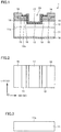
- Fig. 2 shows a schematic plan view of silicon carbide semiconductor device 1 shown in Fig. 1 as seen from gate electrode 17 side.
- the surface of source electrode 16 and the surface of gate electrode 17 are formed to extend in a stripe pattern in the ⁇ -2110> direction.
- source electrode 16 and gate electrode 17 are alternately arranged, and one gate electrode 17 is disposed between two source electrodes 16. Further, from a gap between source electrode 16 and gate electrode 17, a surface of insulating film 13 is exposed.
- the channel direction tends to be set easily in a range of ⁇ 10° relative to the direction orthogonal to the ⁇ -2110> direction, in sidewall 19 (crystal plane tilted by an angle in a range of not less than 50° and not more than 65° relative to the ⁇ 0001 ⁇ plane) of trench 20 as described later herein.
- the channel direction means the direction in which carriers move in sidewall 19 of trench 20.
- the channel direction of silicon carbide semiconductor device 1 with the above-described structure is set to be included in a range of ⁇ 10° relative to the direction orthogonal to the ⁇ -2110> direction, in sidewall 19 of trench 20 that is formed of a crystal plane tilted by an angle in a range of not less than 50° and not more than 65° relative to the ⁇ 0001 ⁇ plane.
- substrate 11 made of silicon carbide (4H-SiC) having surface 11a formed of a crystal plane that is a ⁇ 2-1-10 ⁇ plane for example is prepared.
- semiconductor layer 12 is formed on surface 11a of substrate 11.
- semiconductor layer 12 may be formed for example by epitaxial growth or the like of semiconductor layer 12 made of n-type silicon carbide having an n-type impurity with a lower concentration than substrate 11, on surface 11a of substrate 11.
- semiconductor layer 12 is formed by the above-described epitaxial growth
- surface 12a of semiconductor layer 12 is allowed to have the same crystal plane as surface 11a of substrate 11. Therefore, if surface 11a of substrate 11 is formed for example of a crystal plane that is a ⁇ 2-1-10 ⁇ plane, surface 12a of semiconductor layer 12 is allowed to have a crystal plane that is a ⁇ 2-1-10 ⁇ plane as well, as shown in the schematic plan view of Fig. 5 for example.
- second-conductive-type impurity diffusion layer 14 is formed in surface 12a of semiconductor layer 12.
- second-conductive-type impurity diffusion layer 14 is formed in a stripe pattern extending in the ⁇ -2110> direction.
- Second-conductive-type impurity diffusion layer 14, however, is not limited to this form.
- second-conductive-type impurity diffusion layer 14 may be formed for example by ion implantation or the like in which ions of a p-type impurity serving as a second-conductive-type impurity are implanted into surface 12a of semiconductor layer 12, after an ion implantation block mask is placed in a region other than the region where second-conductive-type impurity diffusion layer 14 is to be formed in surface 12a of semiconductor layer 12.
- an oxide film or the like that has been patterned by photolithography and etching for example may be used.
- first-conductive-type impurity diffusion layer 15 is formed in a surface of second-conductive-type impurity diffusion layer 14 formed in the above-described manner.
- first-conductive-type impurity diffusion layer 15 is also formed in a stripe pattern extending in the ⁇ -2110> direction.
- first-conductive-type impurity diffusion layer 15 may be formed for example by ion implantation or the like in which ions of an n-type impurity serving as a first-conductive-type impurity are implanted into surface 12a of semiconductor layer 12, after an ion implantation block mask is placed in a region other than the region where first-conductive-type impurity diffusion layer 15 is to be formed in surface 12a of semiconductor layer 12.
- an oxide film or the like that has been patterned by photolithography and etching for example may be used as well.
- an activation annealing treatment is performed on semiconductor layer 12 in which second-conductive-type impurity diffusion layer 14 and first-conductive-type impurity diffusion layer 15 have been formed in the above-described manner. Accordingly, the p-type impurity serving as a second-conductive-type impurity in second-conductive-type impurity diffusion layer 14 as well as the n-type impurity serving as a first-conductive-type impurity in first-conductive-type impurity diffusion layer 15 that have been introduced by the above-described ion implantation can be activated.
- the activation annealing treatment may be performed for example in an argon gas atmosphere by heating semiconductor layer 12 in which second-conductive-type impurity diffusion layer 14 and first-conductive-type impurity diffusion layer 15 have been formed, at a temperature of approximately 1700°C for approximately 30 minutes, for example.
- trench 20 having sidewall 19 is formed in surface 12a of semiconductor layer 12.
- Trench 20 may be formed for example by providing an etching mask in a region other than the region where trench 20 is to be formed in surface 12a of semiconductor layer 12, and thereafter etching and thereby removing the region of surface 12a of semiconductor layer 12 where the etching mask is not provided.
- the channel direction is to be made coincident with the direction in which sidewall 19 of trench 20 extends
- a defect could be formed at a certain portion of semiconductor layer 12. Therefore, the position of the defect formed at a certain portion of semiconductor layer 12 may be used as a reference. Then, where the channel direction is to be made coincident with the direction in which sidewall 19 of trench 20 extends for example, trench 20 can be formed easily so that the direction in which sidewall 19 of trench 20 extends is included in a range of ⁇ 10° relative to the direction orthogonal to the ⁇ -2110> direction.
- sidewall 19 of trench 20 is formed of a crystal plane (hatched portion in Fig. 10 ) that is tilted at an angle ⁇ ° in a range of not less than 50° and not more than 65° relative to the ⁇ 0001 ⁇ plane.
- the crystal plane of sidewall 19 of trench 20 is also tilted at an angle in a range of ⁇ 5° relative to the ⁇ 03-38 ⁇ plane as shown for example in a schematic cross section of Fig. 11 .
- sidewall 19 of trench 20 is a crystal plane tilted at an angle in a range of ⁇ 5° relative to the ⁇ 03-38 ⁇ plane
- electrical characteristics such as channel mobility of silicon carbide semiconductor device 1 tend to be improved.
- sidewall 19 of trench 20 is a crystal plane tilted at an angle in a range of ⁇ 3° relative to the ⁇ 03-38 ⁇ plane, and most preferably sidewall 19 of trench 20 is the ⁇ 03-38 ⁇ plane.
- a crystal plane tilted at an angle in a range of ⁇ 5° relative to the ⁇ 03-38 ⁇ plane and a crystal plane tilted at an angle in a range of ⁇ 3° relative to the ⁇ 03-38 ⁇ plane each include the ⁇ 03-38 ⁇ plane.
- Insulating film 13 is formed to contact sidewall 19 of trench 20 formed in the above-described manner.
- Insulating film 13 can be formed to contact sidewall 19 of trench 20 that extends in the direction as controlled so that the direction in which sidewall 19 of trench 20 extends is included in a range of ⁇ 10° relative to the direction orthogonal to the ⁇ -2110> direction, and thereby set the channel direction in a range of ⁇ 10° relative to the direction orthogonal to the ⁇ -2110> direction.
- insulating film 13 an oxide film or the like formed for example by dry oxidation (thermal oxidation) or the like may be used.
- dry oxidation thermal oxidation
- a nitrogen annealing treatment is performed on semiconductor layer 12 where above-described insulating film 13 has been formed.
- the nitrogen concentration is adjusted so that a maximum value of the nitrogen concentration in a region within 10 nm from the interface between sidewall 19 of trench 20 and insulating film 13 is not less than 1 ⁇ 10 21 cm -3 .
- semiconductor layer 12 where above-described insulating film 13 has been formed is heated for example in an atmosphere of a gas containing nitrogen such as nitrogen monoxide (NO) gas at a temperature of approximately 1100°C for approximately 120 minutes for example.
- a maximum value of the nitrogen concentration in the region within 10 nm from the interface between sidewall 19 of trench 20 and insulating film 13 can be set to 1 ⁇ 10 21 cm -3 or more.
- an inert gas annealing treatment on semiconductor layer 12 having undergone the above-described nitrogen annealing treatment, in an atmosphere of an inert gas such as argon gas for example.
- an inert gas such as argon gas for example.
- the above-described inert gas annealing treatment may be performed for example in an argon gas atmosphere by heating semiconductor layer 12 having undergone the above-described nitrogen annealing treatment, at a temperature of approximately 1100°C for approximately 60 minutes for example.
- patterning of insulating film 13 is performed by removing a part of insulating film 13 so that at least a part of the surface of first-conductive-type impurity diffusion layer 15 in surface 12a of semiconductor layer 12 is exposed.
- a part of insulating film 13 may be removed for example by forming, on the surface of insulating film 13, an etching mask patterned by means of photolithography and etching for exposing a part to be removed of insulating film 13, for example, and thereafter etching and thereby removing the exposed part of insulating film 13.
- source electrode 16 is formed to contact the exposed surface of first-conductive-type impurity diffusion layer 15 in surface 12a of semiconductor layer 12 that is exposed from the part where insulating film 13 has been removed.
- source electrode 16 may be formed for example by performing sputtering for example to form an electrically conductive film made of a metal such as nickel for example, on surface 12a of semiconductor layer 12 exposed after the above-described etching of insulating film 13 and on the surface of the above-described etching mask, and thereafter removing this etching mask.
- the conductive film formed on the surface of the etching mask is removed (lifted off) together with the etching mask while only the conductive film formed on surface 12a of semiconductor layer 12 is left to serve as source electrode 16.
- a heat treatment for achieving alloying is performed on semiconductor layer 12 on which above-described source electrode 16 has been formed.
- the heat treatment for achieving alloying may be performed for example in an atmosphere of an inert gas such as argon gas by heating semiconductor layer 12 on which above-described source electrode 16 has been formed, at a temperature of approximately 950°C for approximately two minutes for example.
- an inert gas such as argon gas
- gate electrode 17 is formed on a surface of insulating film 13.
- gate electrode 17 may be formed for example by performing photolithography and etching or the like to form a resist mask having an opening corresponding to a portion where gate electrode 17 is to be formed and covering respective entire surfaces of insulating film 13 and source electrode 16, then performing for example sputtering or the like to form an electrically conductive film made of a metal such as aluminum for example, on the surface of the resist mask and on the surface of insulating film 13 that is exposed from the opening of the resist mask, and thereafter removing this resist mask.
- the conductive film formed on the surface of the resist mask is removed (lifted off) together with the resist mask while only the conductive film formed on the surface of insulating film 13 is left to serve as gate electrode 17.
- drain electrode 18 is formed on the back surface of substrate 11.
- drain electrode 18 may be formed for example by performing for example sputtering or the like to form an electrically conductive film made of a metal such as nickel for example, on the back surface of substrate 11.
- silicon carbide semiconductor device 1 with the structure shown in Fig. 1 can be manufactured.
- the surface of source electrode 16 may be formed in a honeycomb pattern and a region except for a partial region surrounding the outer periphery of source electrode 16 may be formed as gate electrode 17 as shown for example in a schematic plan view of Fig. 14 .
- each source electrode 16 is formed in the shape of a hexagon.
- the surface of source electrode 16 is preferably formed in the shape of a regular hexagon.
- the possible number of silicon carbide semiconductor devices 1 to be formed from substrate 11 of the same size can be increased. Therefore, there is a tendency that silicon carbide semiconductor device 1 having a high channel mobility can be fabricated with higher reproducibility and at a higher manufacturing efficiency.
- second-conductive-type impurity diffusion layer 14 and first-conductive-type impurity diffusion layer 15 may also be formed in a hexagonal shape such as regular hexagonal shape.
- silicon carbide semiconductor device 1 having source electrode 16 and gate electrode 17 structured as shown in Fig. 14 may be similar to the above-described ones.
- silicon carbide semiconductor device 1 structured in the above-described manner, when a negative voltage is applied to source electrode 16 and a positive voltage is applied to gate electrode 17 and drain electrode 18 for example, carriers (electrons in the above-described example) injected from source electrode 16 move to drain electrode 18 through the surface of first-conductive-type impurity diffusion layer 15, sidewall 19 of trench 20, the inside of semiconductor layer 12, and the inside of substrate 11.
- a maximum value of the nitrogen concentration in a region within 10 nm from the interface between sidewall 19 of trench 20 and insulating film 13 is not less than 1 ⁇ 10 21 cm -3 as shown for example in Fig. 15 . Therefore, in silicon carbide semiconductor device 1 of the present invention, the number of interface states that occur when insulating film 13 is formed by dry oxidation (thermal oxidation) or the like at the interface between sidewall 19 of trench 20 and insulating film 13 can be reduced. Accordingly, particularly in a channel directly below insulating film 13 (the portion of sidewall 19 of trench 20 contacting insulating film 13), the carrier mobility (channel mobility) can stably be improved.
- Fig. 15 shows an example of the nitrogen concentration in the vicinity of the interface between sidewall 19 of trench 20 and insulating film 13 in silicon carbide semiconductor device 1 with the above-described structure.
- the vertical axis represents the nitrogen concentration (cm -3 ) and the horizontal axis represents the distance (nm) from the interface between sidewall 19 of trench 20 and insulating film 13.
- the portion where the distance (nm) on the horizontal axis is 0 (nm) represents the interface between sidewall 19 of trench 20 and insulating film 13.
- the extension in the leftward direction with respect to the portion of 0 (nm) on the horizontal axis of the distance (nm) represents extension in the direction toward insulating film 13 side, while the extension in the rightward direction with respect to the portion of 0 (nm) on the horizontal axis of the distance (nm) represents extension in the direction toward sidewall 19 side of trench 20.
- silicon carbide semiconductor device 1 with the above-described structure has the channel direction in a range of ⁇ 10° relative to the direction orthogonal to the ⁇ -2110> direction in sidewall 19 of trench 20. Carriers therefore move smoothly in this channel direction, and the carrier mobility in this channel direction and electric current characteristics can be improved. Accordingly, the ON resistance of silicon carbide semiconductor device 1 can be reduced.
- Fig. 16 shows an example of the relation between the channel mobility (relative value) and the angle (°) relative to the ⁇ -2110> direction in sidewall 19 of trench 20 (in the crystal plane tilted by an angle in a range of not less than 50° and not more than 65° relative to the ⁇ 0001 ⁇ plane) of silicon carbide semiconductor device 1 with the above-described structure.
- the vertical axis represents the channel mobility (relative value) and the horizontal axis represents the angle (°) relative to the ⁇ -2110> direction in sidewall 19 of trench 20.
- the angle (°) on the horizontal axis in Fig. 16 the angle is not distinguished in terms of the direction of tilt relative to the ⁇ -2110> direction. Therefore, 80° on the horizontal axis for example represents both the direction tilted by +80° relative to the ⁇ -2110> direction and the direction tilted by -80° relative to the ⁇ -2110> direction.
- the channel mobility (relative value) on the vertical axis in Fig. 16 is indicated by a relative value with respect to 1 of the channel mobility in the direction orthogonal to the ⁇ -2110> direction in sidewall 19 of trench 20. Further, the portion where the angle is 90° on the horizontal axis in Fig. 16 indicates the direction orthogonal to the ⁇ -2110> direction in sidewall 19 of trench 20.
- the channel mobility is highest when the channel direction extends in the direction at an angle of 90° relative to the ⁇ -2110> direction (the direction orthogonal to the ⁇ -2110> direction) in sidewall 19 of trench 20, while the channel mobility tends to be smaller as a deviation is larger from the direction orthogonal to the ⁇ -2110> direction in sidewall 19 of trench 20.
- the tendency seen from Fig. 16 is also satisfied by any crystal plane of sidewall 19 of trench 20 that is tilted at an angle in a range of not less than 50° and not more than 65° relative to the ⁇ 0001 ⁇ plane.
- the channel direction orthogonal to the ⁇ -2110> direction in sidewall 19 of trench 20 (crystal plane tilted at an angle in a range of not less than 50° and not more than 65° relative to the ⁇ 0001 ⁇ plane) (namely the direction of ⁇ 0° orthogonal to the ⁇ -2110> direction).
- the channel direction is a direction at an angle of not less than 80° and not more than 90° relative to the ⁇ -2110> direction in sidewall 19 of trench 20 (namely a direction in a range of ⁇ 10° relative to the direction orthogonal to the ⁇ - 2110> direction)
- the channel mobility (relative value) is higher than 0.99. Therefore, even when the channel mobility varies to a certain extent due to a problem or the like in manufacture, the channel mobility would unlikely to be deteriorated to a large extent.
- silicon carbide semiconductor device 1 of the present invention having a channel direction in a range of ⁇ 10° relative to the direction orthogonal to the ⁇ -2110> direction in sidewall 19 of trench 20, a high channel mobility can be achieved with high reproducibility. Further, in order to achieve a high channel mobility with high reproducibility in silicon carbide semiconductor device 1 of the present invention, it is most preferable that the channel direction is set in the direction orthogonal to the ⁇ -2110> direction in sidewall 19 of trench 20 as described above.
- the present invention may be constructed so that the first conductive type is the p-type and the second conductive type is the n-type in the structure of the above-described silicon carbide semiconductor device 1.
- a silicon carbide semiconductor device was formed as a vertical trench gate MOSFET of an Example in the following way.
- substrate 11 formed of an n-type silicon carbide crystal (4H-SiC) with a thickness of 400 ⁇ m was prepared.
- substrate 11 had surface 11a formed of a crystal plane that is a ⁇ 2-1-10 ⁇ plane.
- semiconductor layer 12 (n-type impurity concentration: 5 ⁇ 10 15 cm -3 ) formed of an n-type silicon carbide crystal doped with nitrogen as an n-type impurity was epitaxially grown to a thickness of 10 ⁇ m on surface 11a of substrate 11 by means of CVD (Chemical Vapor Deposition).
- surface 12a of semiconductor layer 12 was formed of a crystal plane that is a ⁇ 2-1-10 ⁇ plane having the ⁇ -2110> direction and the ⁇ 03-38> direction orthogonal to the ⁇ -2110> direction as shown in Fig. 5 .
- second-conductive-type impurity diffusion layer 14 (p-type impurity concentration: 1 ⁇ 10 17 cm -3 ) was formed in surface 12a of semiconductor layer 12.
- second-conductive-type impurity diffusion layer 14 was formed by using photolithography and etching to form a patterned oxide film in a region other than the region where second-conductive-type impurity diffusion layer 14 was to be formed in surface 12a of semiconductor layer 12, and implanting ions of boron as a p-type impurity using the oxide film as an ion implantation block mask.
- Second-conductive-type impurity diffusion layer 14 was formed in a stripe pattern extending in the ⁇ -2110> direction.
- first-conductive-type impurity diffusion layer 15 (n-type impurity concentration: 5 ⁇ 10 19 cm -3 ) and a p+-type region (not shown) (p-type impurity concentration: 3 ⁇ 10 19 cm -3 ) were formed.
- first-conductive-type impurity diffusion layer 15 was formed in a stripe pattern extending in the ⁇ -2110> direction
- the p+-type region was formed in a stripe pattern extending in the ⁇ -2110> direction on the outside of first-conductive-type impurity diffusion layer 15 shown in Fig. 7 to contact first-conductive-type impurity diffusion layer 15.
- First-conductive-type impurity diffusion layer 15 was formed by using photolithography and etching to form a patterned oxide film in a region other than the region where first-conductive-type impurity diffusion layer 15 was to be formed in surface 12a of semiconductor layer 12, and implanting ions of phosphorous as an n-type impurity using the oxide film as an ion implantation block mask.
- the p+-type region was also formed by using photolithography and etching to form a patterned oxide film in a region other than the region where the p+-type region was to be formed in surface 12a of semiconductor layer 12, and implanting ions of boron as a p-type impurity using the oxide film as an ion implantation block mask.
- an activation annealing treatment was performed by heating semiconductor layer 12 in which second-conductive-type impurity diffusion layer 14, first-conductive-type impurity diffusion layer 15, and the p+-type region were formed in the above-described manner, in an argon gas atmosphere at 1700°C for 30 minutes.
- trench 20 having sidewall 19 was formed in surface 12a of semiconductor layer 12.
- Trench 20 may be formed for example by providing an etching mask in a region other than the region where trench 20 was to be formed in surface 12a of semiconductor layer 12, and thereafter performing etching perpendicularly to surface 12a of semiconductor layer 12 to remove the region where the etching mask was not provided and thus trench 20 was to be formed in surface 12a of semiconductor layer 12.
- trench 20 was formed in the following way.
- a defect formed in semiconductor layer 12 was used as a reference to specify the direction orthogonal to the ⁇ -2110> direction. As shown in Fig.
- trench 20 was formed so that the direction of extension of sidewall 19 of trench 20 was included in a range of ⁇ 10° relative to the direction orthogonal to the ⁇ -2110> direction. Accordingly, sidewall 19 of trench 20 was formed of the ⁇ 03-38 ⁇ plane which was a crystal plane tilted at an angle of about 55° relative to the ⁇ 0001 ⁇ plane. Further, sidewall 19 of trench 20 extended perpendicularly to surface 12a ( ⁇ 2-1-10 ⁇ plane) of semiconductor layer 12.
- surface 12a of semiconductor layer 12 was heated in oxygen at 1200°C for 30 minutes to be dry-oxidized (thermally oxidized) and thereby form insulating film 13 contacting the whole of surface 12a of semiconductor layer 12.
- a nitrogen annealing treatment was performed by heating semiconductor layer 12 on which insulating film 13 had been formed, in a nitrogen monoxide (NO) gas atmosphere at 1100°C for 120 minutes.
- NO nitrogen monoxide
- an inert gas annealing treatment was performed by heating semiconductor layer 12 having undergone the above-described nitrogen annealing treatment, in an argon gas atmosphere at 1100°C for 60 minutes.
- insulating film 13 was patterned by removing a part of insulating film 13 so that a part of the surface of first-conductive-type impurity diffusion layer 15 and the surface of the p+-type region (not shown) in surface 12a of semiconductor layer 12 were exposed.
- patterning of insulating film 13 was performed by forming, on the surface of insulating film 13, an etching mask patterned by photolithography and etching in order to expose a part-to-be-removed of insulating film 13, and thereafter etching and thereby removing the exposed part of insulating film 13.
- source electrode 16 was formed that was made of nickel and having its surface in the shape of a regular hexagon as shown in Fig. 14 and a thickness of 0.1 ⁇ m.
- semiconductor layer 12 on which above-described source electrode 16 had been formed was heat-treated for alloying, by being heated in an argon gas atmosphere at 950°C for two minutes.
- gate electrode 17 was formed that was made of aluminum and having a surface shape as shown in Fig. 14 and a thickness of 1 ⁇ m.
- drain electrode 18 of nickel with a thickness of 0.1 ⁇ m was formed.
- silicon carbide semiconductor device 1 was fabricated as a vertical trench gate MOSFET of the Example.
- Silicon carbide semiconductor device 1 to serve as a vertical trench gate MOSFET of the Example fabricated in the above-described manner had a channel length (the length, along the direction in which sidewall 19 extends, of first-conductive-type impurity diffusion layer 15 exposed on sidewall 19 of trench 20) was set to 2 ⁇ m.
- a silicon carbide semiconductor device to serve as a vertical trench gate MOSFET of a Comparative Example was fabricated in a manner similar to the above-described one, except that the channel direction of sidewall 19 of trench 20 in surface 12a was the ⁇ -2110> direction.
- the distribution, in the depth direction, of the nitrogen concentration in the vicinity of the interface between sidewall 19 of trench 20 and insulating film 13 was measured by SIMS (secondary ion mass spectrometry).
- the maximum value of the nitrogen concentration in the vicinity of the interface between sidewall 19 of trench 20 and insulating film 13 was 1 ⁇ 10 21 cm -3 or more in both of respective vertical trench gate MOSFETs of the Example and the Comparative Example. It was thus confirmed that the maximum value of the nitrogen concentration in a region within 10 nm from the interface between sidewall 19 of trench 20 and insulating film 13 was not less than 1 ⁇ 10 21 cm -3 in each of respective vertical trench gate MOSFETs of the Example and the Comparative Example.
- the channel mobility was evaluated.
- Channel mobility ⁇ gm ⁇ L ⁇ d / W ⁇ ⁇ ⁇ VDS
- L represents the channel length
- d represents the thickness of insulating film 13
- W represents the channel width
- ⁇ represents the dielectric constant of insulating film 13.
- the channel mobility of the vertical trench gate MOSFET of the Example was 100 cm 2 /Vs and the channel mobility of the vertical trench gate MOSFET of the Comparative Example was 40 cm 2 /Vs.
- the channel mobility of the vertical trench gate MOSFET of the Example was 2.5 times as high as the channel mobility of the vertical trench gate MOSFET of the Comparative Example, and accordingly the source-drain current value was 2.5 times. Thus, a significant reduction in ON resistance was confirmed.
- the channel mobility is unlikely to considerably decrease even when the channel mobility varies depending on problems in manufacture, and thus a high channel mobility can be achieved with high reproducibility.
- the present invention can provide a silicon carbide semiconductor device that can achieve a high channel mobility with high reproducibility as well as a method of manufacturing the same, the present invention is suitably applicable for example to a vertical trench gate MOSFET and the like in which SiC is used.
Landscapes
- Insulated Gate Type Field-Effect Transistor (AREA)
- Electrodes Of Semiconductors (AREA)
Claims (7)
- Siliziumkarbid-Halbleitervorrichtung (1), umfassend:ein Substrat (11) aus Siliziumkarbid mit einem ersten Leitfähigkeitstyp;eine Halbleiterschicht (12) aus Siliziumkarbid, die den ersten Leitfähigkeitstyp aufweist, die auf dem Substrat (11) ausgebildet ist und die eine Verunreinigung mit dem ersten Leitfähigkeitstyp mit einer niedrigeren Konzentration als das Substrat (11) aufweist,wobei die Halbleiterschicht (12) eine Oberfläche (12a) mit einem Graben (20) umfasst, der eine Seitenwand (19) aufweist, die aus einer Kristallebene gebildet ist, die in einem Winkel in einem Bereich von nicht weniger als 50° und nicht mehr als 65° in Bezug auf eine {0001} Ebene geneigt ist; undeinen Isolierfilm (13), der so ausgebildet ist, dass er mit der Seitenwand (19) des Grabens (20) in Kontakt ist,eine Diffusionsschicht (14) mit einer zweiten Leitfähigkeitstypverunreinigung, die in der Seitenwand (19) des Grabens (20) ausgebildet ist;eine Diffusionsschicht (15) mit der ersten Leitfähigkeitstypverunreinigung, die in der Oberfläche der Halbleiterschicht (12) ausgebildet ist;eine Source-Elektrode (16), die so ausgebildet ist, dass sie mit wenigstens einem Teil eines Gebiets, mit Ausnahme eines Gebiets, in dem der Isolierfilm (13) ausgebildet ist, der Oberfläche (12a) der Halbleiterschicht (12) in Kontakt ist;eine Gate-Elektrode (17), die auf dem Isolierfilm (13) ausgebildet ist; undeine Drain-Elektrode (18), die auf einer Oberfläche des Substrats (11) gegenüber einer Oberfläche des Substrats (11) ausgebildet ist, auf der die Halbleiterschicht (12) ausgebildet ist;dadurch gekennzeichnet, dassein Maximalwert einer Stickstoffkonzentration in einem Bereich innerhalb von 10 nm von einer Grenzfläche zwischen der Seitenwand (19) des Grabens (20) und dem Isolierfilm (13) nicht weniger als 1x1021 cm-3 beträgt,wobei die Siliziumkarbid-Halbleitervorrichtung eine Kanalrichtung in einem Bereich von ±10° relativ zu einer Richtung orthogonal zu einer <-2110> Richtung in der Seitenwand (19) des Grabens (20) aufweist.
- Siliziumkarbid-Halbleitervorrichtung (1) nach Anspruch 1, wobei die Source-Elektrode (16) eine Oberfläche mit einem Streifenmuster aufweist.
- Siliziumkarbid-Halbleitervorrichtung (1) nach Anspruch 1, wobei die Source-Elektrode (16) eine Oberfläche mit einem Wabenmuster aufweist.
- Siliziumkarbid-Halbleitervorrichtung (1) nach Anspruch 1, wobei die Seitenwand (19) des Grabens (20) aus einer Kristallebene gebildet ist, die in einem Winkel von ±5° relativ zu einer {03-38} Ebene geneigt ist.
- Verfahren zur Herstellung einer Siliziumkarbid-Halbleitervorrichtung (1), das die folgenden Schritte umfasst:Bilden eines Substrats (11) aus Siliziumkarbid mit einem ersten Leitfähigkeitstyp;Bilden einer Halbleiterschicht (12) mit dem Leitfähigkeitstyp auf dem Substrat (11), die eine Verunreinigung mit dem ersten Leitfähigkeitstyp mit einer niedrigeren Konzentration als das Substrat (11) aufweist,Bilden eines Grabens (20) mit einer Seitenwand (19), die aus einer Kristallebene gebildet ist, die in einem Winkel in einem Bereich von nicht weniger als 50° und nicht mehr als 65° in Bezug auf eine {0001} Ebene in einer Oberfläche der Halbleiterschicht (12) aus Siliziumkarbid geneigt ist;Bilden einer Diffusionsschicht (14) mit einer zweiten Leitfähigkeitstypverunreinigung, die in der Seitenwand (19) des Grabens (20) ausgebildet ist;Bilden einer Diffusionsschicht (15) mit der ersten Leitfähigkeitstypverunreinigung, die in der Oberfläche der Halbleiterschicht (12) ausgebildet ist;Bilden eines Isolierfilms (13) derart, dass er mit der Seitenwand (19) des Grabens (20) in Kontakt ist, so dass eine Kanalrichtung in einem Bereich von ±10° relativ zu einer Richtung orthogonal zu einer <-2110> Richtung in der Seitenwand (19) des Grabens (20) eingestellt ist; undEinstellen einer Stickstoffkonzentration, so dass ein Maximalwert der Stickstoffkonzentration in einem Bereich innerhalb von 10 nm von einer Grenzfläche zwischen der Seitenwand (19) des Grabens (20) und dem Isolierfilm (13) nicht weniger als 1x1021 cm-3 beträgt,Bilden einer Source-Elektrode (16), die so ausgebildet ist, dass sie mit wenigstens einem Teil eines Gebiets, mit Ausnahme eines Gebiets, in dem der Isolierfilm (13) ausgebildet ist, der Oberfläche (12a) der Halbleiterschicht (12) in Kontakt ist;Bilden einer Gate-Elektrode (17), die auf dem Isolierfilm (13) ausgebildet ist; undBilden einer Drain-Elektrode (18), die auf einer Oberfläche des Substrats (11) gegenüber einer Oberfläche des Substrats (11) ausgebildet ist, auf der die Halbleiterschicht (12) ausgebildet ist.
- Verfahren zur Herstellung einer Siliziumkarbid-Halbleitervorrichtung (1) nach Anspruch 5, wobei der Stickstoffkonzentration-Einstellschritt den Schritt des Durchführens einer Wärmebehandlung in einer stickstoffhaltigen Gasatmosphäre auf der Halbleiterschicht (12), auf der der Isolierfilm (13) gebildet wird, umfasst.
- Verfahren zur Herstellung einer Siliziumkarbid-Halbleitervorrichtung (1) nach Anspruch 6, wobei der Stickstoffkonzentration-Einstellschritt den Schritt des Durchführens einer Wärmebehandlung in einer Inertgas-Atmosphäre auf der Halbleiterschicht (12), die der Wärmebehandlung unterzogen wurde, umfasst.
Applications Claiming Priority (1)
| Application Number | Priority Date | Filing Date | Title |
|---|---|---|---|
| PCT/JP2010/051034 WO2011092808A1 (ja) | 2010-01-27 | 2010-01-27 | 炭化ケイ素半導体装置およびその製造方法 |
Publications (3)
| Publication Number | Publication Date |
|---|---|
| EP2530718A1 EP2530718A1 (de) | 2012-12-05 |
| EP2530718A4 EP2530718A4 (de) | 2014-01-01 |
| EP2530718B1 true EP2530718B1 (de) | 2019-10-23 |
Family
ID=44318326
Family Applications (1)
| Application Number | Title | Priority Date | Filing Date |
|---|---|---|---|
| EP10830926.1A Active EP2530718B1 (de) | 2010-01-27 | 2010-01-27 | Siliciumcarbidhalbleiterbauelement und herstellungsverfahren dafür |
Country Status (7)
| Country | Link |
|---|---|
| US (2) | US8450750B2 (de) |
| EP (1) | EP2530718B1 (de) |
| JP (1) | JPWO2011092808A1 (de) |
| KR (1) | KR20120107838A (de) |
| CN (1) | CN102725849B (de) |
| CA (1) | CA2740244A1 (de) |
| WO (1) | WO2011092808A1 (de) |
Families Citing this family (16)
| Publication number | Priority date | Publication date | Assignee | Title |
|---|---|---|---|---|
| CA2777675A1 (en) | 2010-01-19 | 2011-07-28 | Sumitomo Electric Industries, Ltd. | Silicon carbide semiconductor device and method of manufacturing thereof |
| JP6119100B2 (ja) * | 2012-02-01 | 2017-04-26 | 住友電気工業株式会社 | 炭化珪素半導体装置 |
| JP2013165197A (ja) * | 2012-02-13 | 2013-08-22 | Sumitomo Electric Ind Ltd | 炭化珪素半導体装置および炭化珪素半導体装置の製造方法 |
| JP5867134B2 (ja) | 2012-02-13 | 2016-02-24 | 住友電気工業株式会社 | 炭化珪素半導体装置の製造方法 |
| JP6064366B2 (ja) * | 2012-05-18 | 2017-01-25 | 住友電気工業株式会社 | 半導体装置 |
| JP5875684B2 (ja) * | 2012-07-09 | 2016-03-02 | 株式会社日立製作所 | Mos型電界効果トランジスタ |
| CN104969357B (zh) * | 2013-02-05 | 2019-02-01 | 三菱电机株式会社 | 绝缘栅型碳化硅半导体装置及其制造方法 |
| JP6206012B2 (ja) * | 2013-09-06 | 2017-10-04 | 住友電気工業株式会社 | 炭化珪素半導体装置 |
| JP6237046B2 (ja) * | 2013-09-25 | 2017-11-29 | 住友電気工業株式会社 | 炭化珪素半導体装置およびその製造方法 |
| JP2015072944A (ja) * | 2013-10-01 | 2015-04-16 | 住友電気工業株式会社 | 炭化珪素半導体装置およびその製造方法 |
| JP2015156429A (ja) * | 2014-02-20 | 2015-08-27 | 住友電気工業株式会社 | 炭化珪素半導体装置およびその製造方法 |
| JP6301795B2 (ja) * | 2014-09-19 | 2018-03-28 | 株式会社東芝 | 半導体装置 |
| DE102015103067B3 (de) * | 2015-03-03 | 2016-09-01 | Infineon Technologies Ag | Halbleitervorrichtung mit trenchgatestrukturen in einem halbleiterkörper mit hexagonalem kristallgitter |
| KR102335489B1 (ko) * | 2016-12-13 | 2021-12-03 | 현대자동차 주식회사 | 반도체 소자 및 그 제조 방법 |
| CN111261720A (zh) * | 2018-12-03 | 2020-06-09 | 珠海格力电器股份有限公司 | 半导体器件及其制备方法 |
| CN115513297B (zh) * | 2022-11-09 | 2023-09-22 | 中芯越州集成电路制造(绍兴)有限公司 | 碳化硅平面mosfet器件及其制造方法 |
Family Cites Families (23)
| Publication number | Priority date | Publication date | Assignee | Title |
|---|---|---|---|---|
| JPH0752772B2 (ja) * | 1986-11-22 | 1995-06-05 | ヤマハ株式会社 | 半導体装置の製法 |
| JP3334290B2 (ja) * | 1993-11-12 | 2002-10-15 | 株式会社デンソー | 半導体装置 |
| US5736753A (en) * | 1994-09-12 | 1998-04-07 | Hitachi, Ltd. | Semiconductor device for improved power conversion having a hexagonal-system single-crystal silicon carbide |
| JP3471509B2 (ja) * | 1996-01-23 | 2003-12-02 | 株式会社デンソー | 炭化珪素半導体装置 |
| BR9806136A (pt) * | 1997-08-27 | 1999-10-26 | Matsushita Eletric Industrtial | Substrato de carbureto de silìco e método para a produção do substrato, e dispositivo semicondutor utilizand o substrato. |
| EP1065726B1 (de) * | 1998-03-19 | 2010-01-13 | Hitachi, Ltd. | Sperrschicht-feldeffekttransistor aus silicumcarbid |
| DE60033829T2 (de) * | 1999-09-07 | 2007-10-11 | Sixon Inc. | SiC-HALBLEITERSCHEIBE, SiC-HALBLEITERBAUELEMENT SOWIE HERSTELLUNGSVERFAHREN FÜR EINE SiC-HALBLEITERSCHEIBE |
| JP4450123B2 (ja) | 1999-11-17 | 2010-04-14 | 株式会社デンソー | 炭化珪素半導体装置 |
| EP1187220A3 (de) * | 2000-09-11 | 2007-10-10 | Kabushiki Kaisha Toshiba | MOS-Feldeffekttransistor mit reduziertem Anschaltwiderstand |
| JP4843854B2 (ja) | 2001-03-05 | 2011-12-21 | 住友電気工業株式会社 | Mosデバイス |
| JP2003095797A (ja) | 2001-09-26 | 2003-04-03 | Toshiba Corp | 単結晶材料の製造方法及び電子装置の製造方法 |
| US7709403B2 (en) | 2003-10-09 | 2010-05-04 | Panasonic Corporation | Silicon carbide-oxide layered structure, production method thereof, and semiconductor device |
| JP2005136386A (ja) | 2003-10-09 | 2005-05-26 | Matsushita Electric Ind Co Ltd | 炭化珪素−酸化物積層体,その製造方法及び半導体装置 |
| JP5017768B2 (ja) * | 2004-05-31 | 2012-09-05 | 富士電機株式会社 | 炭化珪素半導体素子 |
| JP4549167B2 (ja) | 2004-11-25 | 2010-09-22 | 三菱電機株式会社 | 炭化珪素半導体装置の製造方法 |
| JP2006210818A (ja) * | 2005-01-31 | 2006-08-10 | Matsushita Electric Ind Co Ltd | 半導体素子およびその製造方法 |
| US7553740B2 (en) * | 2005-05-26 | 2009-06-30 | Fairchild Semiconductor Corporation | Structure and method for forming a minimum pitch trench-gate FET with heavy body region |
| JP5017855B2 (ja) * | 2005-12-14 | 2012-09-05 | 富士電機株式会社 | 半導体装置の製造方法 |
| JPWO2007086196A1 (ja) * | 2006-01-30 | 2009-06-18 | 住友電気工業株式会社 | 炭化珪素半導体装置の製造方法 |
| JP5167593B2 (ja) | 2006-03-23 | 2013-03-21 | 富士電機株式会社 | 半導体装置 |
| JP5157843B2 (ja) * | 2007-12-04 | 2013-03-06 | 住友電気工業株式会社 | 炭化ケイ素半導体装置およびその製造方法 |
| JP5504597B2 (ja) * | 2007-12-11 | 2014-05-28 | 住友電気工業株式会社 | 炭化ケイ素半導体装置およびその製造方法 |
| JP5298691B2 (ja) * | 2008-07-31 | 2013-09-25 | 住友電気工業株式会社 | 炭化ケイ素半導体装置およびその製造方法 |
-
2010
- 2010-01-27 KR KR1020117011408A patent/KR20120107838A/ko not_active Withdrawn
- 2010-01-27 WO PCT/JP2010/051034 patent/WO2011092808A1/ja not_active Ceased
- 2010-01-27 JP JP2011522717A patent/JPWO2011092808A1/ja active Pending
- 2010-01-27 CA CA2740244A patent/CA2740244A1/en not_active Abandoned
- 2010-01-27 US US13/130,986 patent/US8450750B2/en active Active
- 2010-01-27 EP EP10830926.1A patent/EP2530718B1/de active Active
- 2010-01-27 CN CN201080003308.1A patent/CN102725849B/zh active Active
-
2013
- 2013-04-08 US US13/858,904 patent/US20130224941A1/en not_active Abandoned
Non-Patent Citations (1)
| Title |
|---|
| None * |
Also Published As
| Publication number | Publication date |
|---|---|
| CA2740244A1 (en) | 2011-07-27 |
| EP2530718A4 (de) | 2014-01-01 |
| KR20120107838A (ko) | 2012-10-04 |
| US8450750B2 (en) | 2013-05-28 |
| CN102725849A (zh) | 2012-10-10 |
| EP2530718A1 (de) | 2012-12-05 |
| WO2011092808A1 (ja) | 2011-08-04 |
| US20130224941A1 (en) | 2013-08-29 |
| JPWO2011092808A1 (ja) | 2013-05-30 |
| US20110297963A1 (en) | 2011-12-08 |
| CN102725849B (zh) | 2015-09-09 |
Similar Documents
| Publication | Publication Date | Title |
|---|---|---|
| EP2530718B1 (de) | Siliciumcarbidhalbleiterbauelement und herstellungsverfahren dafür | |
| US12057498B2 (en) | Silicon carbide semiconductor device and method for manufacturing same | |
| EP2725622B1 (de) | Siliziumcarbid-halbleiterelement und herstellungsverfahren dafür | |
| US8421151B2 (en) | Semiconductor device and process for production thereof | |
| JP5298691B2 (ja) | 炭化ケイ素半導体装置およびその製造方法 | |
| US8502236B2 (en) | Insulated gate field effect transistor | |
| US7982224B2 (en) | Semiconductor device with silicon carbide epitaxial layer including dopant profiles for reducing current overconcentration | |
| US8525187B2 (en) | Insulated gate bipolar transistor | |
| EP2528098B1 (de) | Siliciumcarbid-halbleiterbauelement und herstellungsverfahren dafür | |
| US20110198616A1 (en) | Semiconductor device and method for manufacturing same | |
| EP2717318A1 (de) | Siliciumcarbid-halbleiterbauelement und herstellungsverfahren dafür | |
| KR20130139739A (ko) | Igbt | |
| KR20140097130A (ko) | 반도체 장치 및 그 제조 방법 | |
| JP5817204B2 (ja) | 炭化珪素半導体装置 | |
| US9728633B2 (en) | Silicon carbide semiconductor device and method for manufacturing the same | |
| US8536583B2 (en) | MOSFET and method for manufacturing MOSFET |
Legal Events
| Date | Code | Title | Description |
|---|---|---|---|
| PUAI | Public reference made under article 153(3) epc to a published international application that has entered the european phase |
Free format text: ORIGINAL CODE: 0009012 |
|
| 17P | Request for examination filed |
Effective date: 20120519 |
|
| AK | Designated contracting states |
Kind code of ref document: A1 Designated state(s): AT BE BG CH CY CZ DE DK EE ES FI FR GB GR HR HU IE IS IT LI LT LU LV MC MK MT NL NO PL PT RO SE SI SK SM TR |
|
| DAX | Request for extension of the european patent (deleted) | ||
| A4 | Supplementary search report drawn up and despatched |
Effective date: 20131203 |
|
| RIC1 | Information provided on ipc code assigned before grant |
Ipc: H01L 29/12 20060101ALI20131127BHEP Ipc: H01L 29/78 20060101AFI20131127BHEP Ipc: H01L 29/04 20060101ALI20131127BHEP Ipc: H01L 21/336 20060101ALI20131127BHEP Ipc: H01L 29/06 20060101ALI20131127BHEP |
|
| STAA | Information on the status of an ep patent application or granted ep patent |
Free format text: STATUS: EXAMINATION IS IN PROGRESS |
|
| 17Q | First examination report despatched |
Effective date: 20180514 |
|
| GRAP | Despatch of communication of intention to grant a patent |
Free format text: ORIGINAL CODE: EPIDOSNIGR1 |
|
| STAA | Information on the status of an ep patent application or granted ep patent |
Free format text: STATUS: GRANT OF PATENT IS INTENDED |
|
| INTG | Intention to grant announced |
Effective date: 20181116 |
|
| GRAJ | Information related to disapproval of communication of intention to grant by the applicant or resumption of examination proceedings by the epo deleted |
Free format text: ORIGINAL CODE: EPIDOSDIGR1 |
|
| STAA | Information on the status of an ep patent application or granted ep patent |
Free format text: STATUS: EXAMINATION IS IN PROGRESS |
|
| INTC | Intention to grant announced (deleted) | ||
| GRAP | Despatch of communication of intention to grant a patent |
Free format text: ORIGINAL CODE: EPIDOSNIGR1 |
|
| STAA | Information on the status of an ep patent application or granted ep patent |
Free format text: STATUS: GRANT OF PATENT IS INTENDED |
|
| INTG | Intention to grant announced |
Effective date: 20190522 |
|
| GRAS | Grant fee paid |
Free format text: ORIGINAL CODE: EPIDOSNIGR3 |
|
| GRAA | (expected) grant |
Free format text: ORIGINAL CODE: 0009210 |
|
| STAA | Information on the status of an ep patent application or granted ep patent |
Free format text: STATUS: THE PATENT HAS BEEN GRANTED |
|
| AK | Designated contracting states |
Kind code of ref document: B1 Designated state(s): AT BE BG CH CY CZ DE DK EE ES FI FR GB GR HR HU IE IS IT LI LT LU LV MC MK MT NL NO PL PT RO SE SI SK SM TR |
|
| REG | Reference to a national code |
Ref country code: GB Ref legal event code: FG4D |
|
| REG | Reference to a national code |
Ref country code: CH Ref legal event code: EP |
|
| REG | Reference to a national code |
Ref country code: IE Ref legal event code: FG4D |
|
| REG | Reference to a national code |
Ref country code: DE Ref legal event code: R096 Ref document number: 602010061670 Country of ref document: DE |
|
| REG | Reference to a national code |
Ref country code: AT Ref legal event code: REF Ref document number: 1194664 Country of ref document: AT Kind code of ref document: T Effective date: 20191115 |
|
| REG | Reference to a national code |
Ref country code: NL Ref legal event code: MP Effective date: 20191023 |
|
| REG | Reference to a national code |
Ref country code: LT Ref legal event code: MG4D |
|
| PG25 | Lapsed in a contracting state [announced via postgrant information from national office to epo] |
Ref country code: NL Free format text: LAPSE BECAUSE OF FAILURE TO SUBMIT A TRANSLATION OF THE DESCRIPTION OR TO PAY THE FEE WITHIN THE PRESCRIBED TIME-LIMIT Effective date: 20191023 Ref country code: SE Free format text: LAPSE BECAUSE OF FAILURE TO SUBMIT A TRANSLATION OF THE DESCRIPTION OR TO PAY THE FEE WITHIN THE PRESCRIBED TIME-LIMIT Effective date: 20191023 Ref country code: LV Free format text: LAPSE BECAUSE OF FAILURE TO SUBMIT A TRANSLATION OF THE DESCRIPTION OR TO PAY THE FEE WITHIN THE PRESCRIBED TIME-LIMIT Effective date: 20191023 Ref country code: PL Free format text: LAPSE BECAUSE OF FAILURE TO SUBMIT A TRANSLATION OF THE DESCRIPTION OR TO PAY THE FEE WITHIN THE PRESCRIBED TIME-LIMIT Effective date: 20191023 Ref country code: NO Free format text: LAPSE BECAUSE OF FAILURE TO SUBMIT A TRANSLATION OF THE DESCRIPTION OR TO PAY THE FEE WITHIN THE PRESCRIBED TIME-LIMIT Effective date: 20200123 Ref country code: GR Free format text: LAPSE BECAUSE OF FAILURE TO SUBMIT A TRANSLATION OF THE DESCRIPTION OR TO PAY THE FEE WITHIN THE PRESCRIBED TIME-LIMIT Effective date: 20200124 Ref country code: ES Free format text: LAPSE BECAUSE OF FAILURE TO SUBMIT A TRANSLATION OF THE DESCRIPTION OR TO PAY THE FEE WITHIN THE PRESCRIBED TIME-LIMIT Effective date: 20191023 Ref country code: LT Free format text: LAPSE BECAUSE OF FAILURE TO SUBMIT A TRANSLATION OF THE DESCRIPTION OR TO PAY THE FEE WITHIN THE PRESCRIBED TIME-LIMIT Effective date: 20191023 Ref country code: BG Free format text: LAPSE BECAUSE OF FAILURE TO SUBMIT A TRANSLATION OF THE DESCRIPTION OR TO PAY THE FEE WITHIN THE PRESCRIBED TIME-LIMIT Effective date: 20200123 Ref country code: FI Free format text: LAPSE BECAUSE OF FAILURE TO SUBMIT A TRANSLATION OF THE DESCRIPTION OR TO PAY THE FEE WITHIN THE PRESCRIBED TIME-LIMIT Effective date: 20191023 Ref country code: PT Free format text: LAPSE BECAUSE OF FAILURE TO SUBMIT A TRANSLATION OF THE DESCRIPTION OR TO PAY THE FEE WITHIN THE PRESCRIBED TIME-LIMIT Effective date: 20200224 |
|
| PG25 | Lapsed in a contracting state [announced via postgrant information from national office to epo] |
Ref country code: IS Free format text: LAPSE BECAUSE OF FAILURE TO SUBMIT A TRANSLATION OF THE DESCRIPTION OR TO PAY THE FEE WITHIN THE PRESCRIBED TIME-LIMIT Effective date: 20200224 Ref country code: HR Free format text: LAPSE BECAUSE OF FAILURE TO SUBMIT A TRANSLATION OF THE DESCRIPTION OR TO PAY THE FEE WITHIN THE PRESCRIBED TIME-LIMIT Effective date: 20191023 |
|
| REG | Reference to a national code |
Ref country code: DE Ref legal event code: R097 Ref document number: 602010061670 Country of ref document: DE |
|
| PG2D | Information on lapse in contracting state deleted |
Ref country code: IS |
|
| PG25 | Lapsed in a contracting state [announced via postgrant information from national office to epo] |
Ref country code: CZ Free format text: LAPSE BECAUSE OF FAILURE TO SUBMIT A TRANSLATION OF THE DESCRIPTION OR TO PAY THE FEE WITHIN THE PRESCRIBED TIME-LIMIT Effective date: 20191023 Ref country code: EE Free format text: LAPSE BECAUSE OF FAILURE TO SUBMIT A TRANSLATION OF THE DESCRIPTION OR TO PAY THE FEE WITHIN THE PRESCRIBED TIME-LIMIT Effective date: 20191023 Ref country code: DK Free format text: LAPSE BECAUSE OF FAILURE TO SUBMIT A TRANSLATION OF THE DESCRIPTION OR TO PAY THE FEE WITHIN THE PRESCRIBED TIME-LIMIT Effective date: 20191023 Ref country code: RO Free format text: LAPSE BECAUSE OF FAILURE TO SUBMIT A TRANSLATION OF THE DESCRIPTION OR TO PAY THE FEE WITHIN THE PRESCRIBED TIME-LIMIT Effective date: 20191023 Ref country code: IS Free format text: LAPSE BECAUSE OF FAILURE TO SUBMIT A TRANSLATION OF THE DESCRIPTION OR TO PAY THE FEE WITHIN THE PRESCRIBED TIME-LIMIT Effective date: 20200223 |
|
| REG | Reference to a national code |
Ref country code: AT Ref legal event code: MK05 Ref document number: 1194664 Country of ref document: AT Kind code of ref document: T Effective date: 20191023 |
|
| PLBE | No opposition filed within time limit |
Free format text: ORIGINAL CODE: 0009261 |
|
| STAA | Information on the status of an ep patent application or granted ep patent |
Free format text: STATUS: NO OPPOSITION FILED WITHIN TIME LIMIT |
|
| PG25 | Lapsed in a contracting state [announced via postgrant information from national office to epo] |
Ref country code: IT Free format text: LAPSE BECAUSE OF FAILURE TO SUBMIT A TRANSLATION OF THE DESCRIPTION OR TO PAY THE FEE WITHIN THE PRESCRIBED TIME-LIMIT Effective date: 20191023 Ref country code: MC Free format text: LAPSE BECAUSE OF FAILURE TO SUBMIT A TRANSLATION OF THE DESCRIPTION OR TO PAY THE FEE WITHIN THE PRESCRIBED TIME-LIMIT Effective date: 20191023 Ref country code: SK Free format text: LAPSE BECAUSE OF FAILURE TO SUBMIT A TRANSLATION OF THE DESCRIPTION OR TO PAY THE FEE WITHIN THE PRESCRIBED TIME-LIMIT Effective date: 20191023 Ref country code: SM Free format text: LAPSE BECAUSE OF FAILURE TO SUBMIT A TRANSLATION OF THE DESCRIPTION OR TO PAY THE FEE WITHIN THE PRESCRIBED TIME-LIMIT Effective date: 20191023 |
|
| REG | Reference to a national code |
Ref country code: CH Ref legal event code: PL |
|
| GBPC | Gb: european patent ceased through non-payment of renewal fee |
Effective date: 20200127 |
|
| 26N | No opposition filed |
Effective date: 20200724 |
|
| REG | Reference to a national code |
Ref country code: BE Ref legal event code: MM Effective date: 20200131 |
|
| PG25 | Lapsed in a contracting state [announced via postgrant information from national office to epo] |
Ref country code: LU Free format text: LAPSE BECAUSE OF NON-PAYMENT OF DUE FEES Effective date: 20200127 Ref country code: FR Free format text: LAPSE BECAUSE OF NON-PAYMENT OF DUE FEES Effective date: 20200131 Ref country code: GB Free format text: LAPSE BECAUSE OF NON-PAYMENT OF DUE FEES Effective date: 20200127 |
|
| PG25 | Lapsed in a contracting state [announced via postgrant information from national office to epo] |
Ref country code: BE Free format text: LAPSE BECAUSE OF NON-PAYMENT OF DUE FEES Effective date: 20200131 Ref country code: SI Free format text: LAPSE BECAUSE OF FAILURE TO SUBMIT A TRANSLATION OF THE DESCRIPTION OR TO PAY THE FEE WITHIN THE PRESCRIBED TIME-LIMIT Effective date: 20191023 Ref country code: CH Free format text: LAPSE BECAUSE OF NON-PAYMENT OF DUE FEES Effective date: 20200131 Ref country code: LI Free format text: LAPSE BECAUSE OF NON-PAYMENT OF DUE FEES Effective date: 20200131 Ref country code: AT Free format text: LAPSE BECAUSE OF FAILURE TO SUBMIT A TRANSLATION OF THE DESCRIPTION OR TO PAY THE FEE WITHIN THE PRESCRIBED TIME-LIMIT Effective date: 20191023 |
|
| PG25 | Lapsed in a contracting state [announced via postgrant information from national office to epo] |
Ref country code: IE Free format text: LAPSE BECAUSE OF NON-PAYMENT OF DUE FEES Effective date: 20200127 |
|
| PG25 | Lapsed in a contracting state [announced via postgrant information from national office to epo] |
Ref country code: TR Free format text: LAPSE BECAUSE OF FAILURE TO SUBMIT A TRANSLATION OF THE DESCRIPTION OR TO PAY THE FEE WITHIN THE PRESCRIBED TIME-LIMIT Effective date: 20191023 Ref country code: MT Free format text: LAPSE BECAUSE OF FAILURE TO SUBMIT A TRANSLATION OF THE DESCRIPTION OR TO PAY THE FEE WITHIN THE PRESCRIBED TIME-LIMIT Effective date: 20191023 Ref country code: CY Free format text: LAPSE BECAUSE OF FAILURE TO SUBMIT A TRANSLATION OF THE DESCRIPTION OR TO PAY THE FEE WITHIN THE PRESCRIBED TIME-LIMIT Effective date: 20191023 |
|
| PG25 | Lapsed in a contracting state [announced via postgrant information from national office to epo] |
Ref country code: MK Free format text: LAPSE BECAUSE OF FAILURE TO SUBMIT A TRANSLATION OF THE DESCRIPTION OR TO PAY THE FEE WITHIN THE PRESCRIBED TIME-LIMIT Effective date: 20191023 |
|
| P01 | Opt-out of the competence of the unified patent court (upc) registered |
Effective date: 20230515 |
|
| REG | Reference to a national code |
Ref country code: DE Ref legal event code: R079 Ref document number: 602010061670 Country of ref document: DE Free format text: PREVIOUS MAIN CLASS: H01L0029780000 Ipc: H10D0030600000 |
|
| PGFP | Annual fee paid to national office [announced via postgrant information from national office to epo] |
Ref country code: DE Payment date: 20251203 Year of fee payment: 17 |