EP2426484A2 - Gassensor mit metalloxidnanopartikeln und herstellungsverfahren dafür - Google Patents
Gassensor mit metalloxidnanopartikeln und herstellungsverfahren dafür Download PDFInfo
- Publication number
- EP2426484A2 EP2426484A2 EP10769981A EP10769981A EP2426484A2 EP 2426484 A2 EP2426484 A2 EP 2426484A2 EP 10769981 A EP10769981 A EP 10769981A EP 10769981 A EP10769981 A EP 10769981A EP 2426484 A2 EP2426484 A2 EP 2426484A2
- Authority
- EP
- European Patent Office
- Prior art keywords
- gas sensor
- sensor
- metal oxide
- thin layer
- oxide nanoparticles
- Prior art date
- Legal status (The legal status is an assumption and is not a legal conclusion. Google has not performed a legal analysis and makes no representation as to the accuracy of the status listed.)
- Granted
Links
Images
Classifications
-
- G—PHYSICS
- G01—MEASURING; TESTING
- G01N—INVESTIGATING OR ANALYSING MATERIALS BY DETERMINING THEIR CHEMICAL OR PHYSICAL PROPERTIES
- G01N27/00—Investigating or analysing materials by the use of electric, electrochemical, or magnetic means
- G01N27/02—Investigating or analysing materials by the use of electric, electrochemical, or magnetic means by investigating impedance
- G01N27/04—Investigating or analysing materials by the use of electric, electrochemical, or magnetic means by investigating impedance by investigating resistance
- G01N27/12—Investigating or analysing materials by the use of electric, electrochemical, or magnetic means by investigating impedance by investigating resistance of a solid body in dependence upon absorption of a fluid; of a solid body in dependence upon reaction with a fluid, for detecting components in the fluid
-
- B—PERFORMING OPERATIONS; TRANSPORTING
- B05—SPRAYING OR ATOMISING IN GENERAL; APPLYING FLUENT MATERIALS TO SURFACES, IN GENERAL
- B05B—SPRAYING APPARATUS; ATOMISING APPARATUS; NOZZLES
- B05B5/00—Electrostatic spraying apparatus; Spraying apparatus with means for charging the spray electrically; Apparatus for spraying liquids or other fluent materials by other electric means
- B05B5/025—Discharge apparatus, e.g. electrostatic spray guns
- B05B5/0255—Discharge apparatus, e.g. electrostatic spray guns spraying and depositing by electrostatic forces only
-
- C—CHEMISTRY; METALLURGY
- C23—COATING METALLIC MATERIAL; COATING MATERIAL WITH METALLIC MATERIAL; CHEMICAL SURFACE TREATMENT; DIFFUSION TREATMENT OF METALLIC MATERIAL; COATING BY VACUUM EVAPORATION, BY SPUTTERING, BY ION IMPLANTATION OR BY CHEMICAL VAPOUR DEPOSITION, IN GENERAL; INHIBITING CORROSION OF METALLIC MATERIAL OR INCRUSTATION IN GENERAL
- C23C—COATING METALLIC MATERIAL; COATING MATERIAL WITH METALLIC MATERIAL; SURFACE TREATMENT OF METALLIC MATERIAL BY DIFFUSION INTO THE SURFACE, BY CHEMICAL CONVERSION OR SUBSTITUTION; COATING BY VACUUM EVAPORATION, BY SPUTTERING, BY ION IMPLANTATION OR BY CHEMICAL VAPOUR DEPOSITION, IN GENERAL
- C23C24/00—Coating starting from inorganic powder
- C23C24/02—Coating starting from inorganic powder by application of pressure only
- C23C24/04—Impact or kinetic deposition of particles
-
- B—PERFORMING OPERATIONS; TRANSPORTING
- B82—NANOTECHNOLOGY
- B82B—NANOSTRUCTURES FORMED BY MANIPULATION OF INDIVIDUAL ATOMS, MOLECULES, OR LIMITED COLLECTIONS OF ATOMS OR MOLECULES AS DISCRETE UNITS; MANUFACTURE OR TREATMENT THEREOF
- B82B3/00—Manufacture or treatment of nanostructures by manipulation of individual atoms or molecules, or limited collections of atoms or molecules as discrete units
-
- C—CHEMISTRY; METALLURGY
- C23—COATING METALLIC MATERIAL; COATING MATERIAL WITH METALLIC MATERIAL; CHEMICAL SURFACE TREATMENT; DIFFUSION TREATMENT OF METALLIC MATERIAL; COATING BY VACUUM EVAPORATION, BY SPUTTERING, BY ION IMPLANTATION OR BY CHEMICAL VAPOUR DEPOSITION, IN GENERAL; INHIBITING CORROSION OF METALLIC MATERIAL OR INCRUSTATION IN GENERAL
- C23C—COATING METALLIC MATERIAL; COATING MATERIAL WITH METALLIC MATERIAL; SURFACE TREATMENT OF METALLIC MATERIAL BY DIFFUSION INTO THE SURFACE, BY CHEMICAL CONVERSION OR SUBSTITUTION; COATING BY VACUUM EVAPORATION, BY SPUTTERING, BY ION IMPLANTATION OR BY CHEMICAL VAPOUR DEPOSITION, IN GENERAL
- C23C24/00—Coating starting from inorganic powder
-
- C—CHEMISTRY; METALLURGY
- C23—COATING METALLIC MATERIAL; COATING MATERIAL WITH METALLIC MATERIAL; CHEMICAL SURFACE TREATMENT; DIFFUSION TREATMENT OF METALLIC MATERIAL; COATING BY VACUUM EVAPORATION, BY SPUTTERING, BY ION IMPLANTATION OR BY CHEMICAL VAPOUR DEPOSITION, IN GENERAL; INHIBITING CORROSION OF METALLIC MATERIAL OR INCRUSTATION IN GENERAL
- C23C—COATING METALLIC MATERIAL; COATING MATERIAL WITH METALLIC MATERIAL; SURFACE TREATMENT OF METALLIC MATERIAL BY DIFFUSION INTO THE SURFACE, BY CHEMICAL CONVERSION OR SUBSTITUTION; COATING BY VACUUM EVAPORATION, BY SPUTTERING, BY ION IMPLANTATION OR BY CHEMICAL VAPOUR DEPOSITION, IN GENERAL
- C23C24/00—Coating starting from inorganic powder
- C23C24/02—Coating starting from inorganic powder by application of pressure only
-
- C—CHEMISTRY; METALLURGY
- C23—COATING METALLIC MATERIAL; COATING MATERIAL WITH METALLIC MATERIAL; CHEMICAL SURFACE TREATMENT; DIFFUSION TREATMENT OF METALLIC MATERIAL; COATING BY VACUUM EVAPORATION, BY SPUTTERING, BY ION IMPLANTATION OR BY CHEMICAL VAPOUR DEPOSITION, IN GENERAL; INHIBITING CORROSION OF METALLIC MATERIAL OR INCRUSTATION IN GENERAL
- C23C—COATING METALLIC MATERIAL; COATING MATERIAL WITH METALLIC MATERIAL; SURFACE TREATMENT OF METALLIC MATERIAL BY DIFFUSION INTO THE SURFACE, BY CHEMICAL CONVERSION OR SUBSTITUTION; COATING BY VACUUM EVAPORATION, BY SPUTTERING, BY ION IMPLANTATION OR BY CHEMICAL VAPOUR DEPOSITION, IN GENERAL
- C23C26/00—Coating not provided for in groups C23C2/00 - C23C24/00
-
- C—CHEMISTRY; METALLURGY
- C23—COATING METALLIC MATERIAL; COATING MATERIAL WITH METALLIC MATERIAL; CHEMICAL SURFACE TREATMENT; DIFFUSION TREATMENT OF METALLIC MATERIAL; COATING BY VACUUM EVAPORATION, BY SPUTTERING, BY ION IMPLANTATION OR BY CHEMICAL VAPOUR DEPOSITION, IN GENERAL; INHIBITING CORROSION OF METALLIC MATERIAL OR INCRUSTATION IN GENERAL
- C23C—COATING METALLIC MATERIAL; COATING MATERIAL WITH METALLIC MATERIAL; SURFACE TREATMENT OF METALLIC MATERIAL BY DIFFUSION INTO THE SURFACE, BY CHEMICAL CONVERSION OR SUBSTITUTION; COATING BY VACUUM EVAPORATION, BY SPUTTERING, BY ION IMPLANTATION OR BY CHEMICAL VAPOUR DEPOSITION, IN GENERAL
- C23C4/00—Coating by spraying the coating material in the molten state, e.g. by flame, plasma or electric discharge
- C23C4/04—Coating by spraying the coating material in the molten state, e.g. by flame, plasma or electric discharge characterised by the coating material
- C23C4/10—Oxides, borides, carbides, nitrides or silicides; Mixtures thereof
-
- C—CHEMISTRY; METALLURGY
- C23—COATING METALLIC MATERIAL; COATING MATERIAL WITH METALLIC MATERIAL; CHEMICAL SURFACE TREATMENT; DIFFUSION TREATMENT OF METALLIC MATERIAL; COATING BY VACUUM EVAPORATION, BY SPUTTERING, BY ION IMPLANTATION OR BY CHEMICAL VAPOUR DEPOSITION, IN GENERAL; INHIBITING CORROSION OF METALLIC MATERIAL OR INCRUSTATION IN GENERAL
- C23C—COATING METALLIC MATERIAL; COATING MATERIAL WITH METALLIC MATERIAL; SURFACE TREATMENT OF METALLIC MATERIAL BY DIFFUSION INTO THE SURFACE, BY CHEMICAL CONVERSION OR SUBSTITUTION; COATING BY VACUUM EVAPORATION, BY SPUTTERING, BY ION IMPLANTATION OR BY CHEMICAL VAPOUR DEPOSITION, IN GENERAL
- C23C4/00—Coating by spraying the coating material in the molten state, e.g. by flame, plasma or electric discharge
- C23C4/18—After-treatment
-
- G—PHYSICS
- G01—MEASURING; TESTING
- G01N—INVESTIGATING OR ANALYSING MATERIALS BY DETERMINING THEIR CHEMICAL OR PHYSICAL PROPERTIES
- G01N27/00—Investigating or analysing materials by the use of electric, electrochemical, or magnetic means
- G01N27/02—Investigating or analysing materials by the use of electric, electrochemical, or magnetic means by investigating impedance
- G01N27/04—Investigating or analysing materials by the use of electric, electrochemical, or magnetic means by investigating impedance by investigating resistance
- G01N27/12—Investigating or analysing materials by the use of electric, electrochemical, or magnetic means by investigating impedance by investigating resistance of a solid body in dependence upon absorption of a fluid; of a solid body in dependence upon reaction with a fluid, for detecting components in the fluid
- G01N27/125—Composition of the body, e.g. the composition of its sensitive layer
- G01N27/127—Composition of the body, e.g. the composition of its sensitive layer comprising nanoparticles
-
- G—PHYSICS
- G01—MEASURING; TESTING
- G01N—INVESTIGATING OR ANALYSING MATERIALS BY DETERMINING THEIR CHEMICAL OR PHYSICAL PROPERTIES
- G01N33/00—Investigating or analysing materials by specific methods not covered by groups G01N1/00 - G01N31/00
- G01N33/0004—Gaseous mixtures, e.g. polluted air
- G01N33/0009—General constructional details of gas analysers, e.g. portable test equipment
- G01N33/0027—General constructional details of gas analysers, e.g. portable test equipment concerning the detector
- G01N33/0036—General constructional details of gas analysers, e.g. portable test equipment concerning the detector specially adapted to detect a particular component
-
- B—PERFORMING OPERATIONS; TRANSPORTING
- B82—NANOTECHNOLOGY
- B82Y—SPECIFIC USES OR APPLICATIONS OF NANOSTRUCTURES; MEASUREMENT OR ANALYSIS OF NANOSTRUCTURES; MANUFACTURE OR TREATMENT OF NANOSTRUCTURES
- B82Y15/00—Nanotechnology for interacting, sensing or actuating, e.g. quantum dots as markers in protein assays or molecular motors
Definitions
- the present invention relates to a gas sensor and a method of manufacturing the same. More particularly, the present invention relates to a gas sensor, which can ultrasensitively detect hydrogen (H 2 ), oxygen (O 2 ) and harmful environmental gases (NO x , CO, CO 2 , HC, SO x , VOCs, etc.) using a metal oxide nanoparticle thin layer formed by spraying a solution containing metal oxide nanoparticles, and to a method of manufacturing the same.
- H 2 hydrogen
- O 2 oxygen
- NO x harmful environmental gases
- metal oxide semiconductor gas sensors measure the concentration of gases by detecting the change in resistance occurring when external gases are adsorbed onto the surface of metal oxides.
- metal oxides ZnO, SnO 2 , WO 3 , TiO 2 , etc.
- materials having a band-gap of 3.0 ⁇ 4.8 eV have semiconductor properties.
- external gases NO x , CO, H 2 , HC, SO x , etc.
- the sensitivity of a sensor increases as the change in resistance of the metal oxide increases. Therefore, in order to improve the sensitivity of a sensor, it is preferable to increase the specific surface area of a metal oxide and to allow a sensor to have a porous structure such that gas easily moves on the surface of a metal oxide.
- Nanowires or nanotubes are characterized in that they can be fabricated in the form of an ultrasensitive nanosensor because the specific surface area of nanowires or nanotubes is relatively large.
- forming such nanostructures is generally accompanied by complicated processes and heat treatment must be conducted at a high temperature of 600°C or above.
- a sensor material including a gas-sensitive material into a thin layer.
- a thin layer is generally formed by screen printing, spin coating, sputtering, pulsed laser deposition (PLD), chemical vapor deposition (CVD) or the like. Further, the thin layer may be formed by an electrospray process.
- Screen printing is problematic in that it is difficult to form a sensor material layer to a thickness of less than 500 nm, and in that additional heat treatment is required in order to remove a binder and improve the adhesiveness between the sensor material layer and a substrate after screen printing.
- U.S. Pat. No. 7,259,109 discloses a method of forming a thin film by preparing a precursor-containing solution and then directly spraying the solution onto a semiconductor substrate.
- this method is used to form a thin film having a low dielectric constant.
- Korean Patent Registration No. 10-0843191 discloses a method of manufacturing a nanofiber fiter medium containing silver nanoparticles, comprising the steps of: forming a nanofiber layer by electrospinning; and electrospraying a silver nanoparticle-containing solution onto the nanofiber layer to diffuse silver nanoparticles into the surface of the nanofiber layer.
- this method only silver nanoparticles are used as the metal nanoparticles.
- Korean Patent Registration No. 10-0583910 discloses a method for patterning nanosized structures by electrospraying nanoparticles in order to overcome the limit of the line width of a pattern, to maintain high reproducibility and solve the problem of noise pattern occurrence.
- gold nanoparticles having a size of 20 nm are used as metal nanoparticles.
- the metal particles such as silver (Ag) particles, gold (Au) particles and the like, mentioned in the above Patent documents, react with environmental pollutants, such as alcohols, NO x , SO x , NH 3 , CO 2 , DMMP, phenol, acetone, formaldehyde, hydrogen gas and the like, it is difficult for them to change the resistance. Therefore, they cannot be used as sensor materials.
- environmental pollutants such as alcohols, NO x , SO x , NH 3 , CO 2 , DMMP, phenol, acetone, formaldehyde, hydrogen gas and the like
- a thin film, formed by electrospraying a solution in which metal ions as metal oxide precursors are dissolved has a surface structure which is not greatly different from that of a sensor thin layer obtained by a general sol-gel reaction or a sensor thin layer formed by sputtering or chemical vapor deposition (CVD), and has high density. Therefore, there is a problem in that it is difficult to manufacture an ultrasensitive sensor which can measure harmful gases at the ppm sensitivity level.
- a first object of the present invention is to provide a high-sensitive gas sensor, which includes a sensor material that has a porous structure and contains metal oxide nanoparticles having a large specific surface area, and which can detect harmful gases at the ppb level.
- a second object of the present invention is to provide an ultrasensitive gas sensor, which has high mechanical and electrical stability because the adhesivity between a sensor substrate provided with an electrode and a sensor material containing metal oxide nanoparticles is greatly increased.
- a third object of the present invention is to provide a method of manufacturing a gas sensor, which can manufacture the above-mentioned high-sensitive gas sensor at room temperature, which can easily adjust the thickness of a sensor material to form a thin film or a thick film, and, if necessary, which can adjust the characteristics of a sensor material by conducting heat treatment.
- a fourth object of the present invention is to provide a method of manufacturing a gas sensor, which can produce the above-mentioned high-sensitive gas sensor in a high yield and at low cost using a simple process.
- an aspect of the present invention provides a gas sensor, including: a sensor substrate provided with an electrode; and a thin layer of sensor material formed by spraying a solution in which metal oxide nanoparticles are dispersed onto the sensor substrate.
- Another aspect of the present invention provides a method of manufacturing a gas sensor, including the steps of preparing a solution in which metal oxide nanoparticles are uniformly dispersed in a solvent; and spraying the solution onto a sensor substrate provided with an electrode to form a thin layer of sensor material.
- the method may further include the step of heat-treating the sensor material at a temperature of 80 °C ⁇ 300 °C.
- the method may further include the step of heat-treating the sensor material at a temperature of 350°C ⁇ 600 °C.
- the method may further include the step of adhering the sensor material closely to the sensor substrate by thermal pressing.
- the gas sensor of the present invention since a sensor material is formed in a porous thin layer containing metal oxide nanoparticles having a large specific surface area, the gas sensor can realize the high sensitivity of ppb and a high reaction rate.
- the gas sensor of the present invention since the gas sensor can be applied to various kinds of gases by changing the kinds of metal oxide nanoparticles used as the material of the sensor, it is possible to impart the gas sensor with the ability to be selective to specific gases.
- the gas sensor of the present invention since the gas sensor is manufactured by directly spraying metal oxide nanoparticles onto a sensor electrode by electrostatic spray deposition, the adhesivity between a sensor substrate and a thin layer composed of metal oxide nanoparticles is greatly improved, and thus the electrical and mechanical stability of the gas sensor becomes high.
- a gas sensor can be manufactured easily and cheaply because the gas sensor is manufactured by electrostatic spray deposition at room temperature. Further, in this method, it is possible to easily form a metal oxide thin layer having a thickness of 10 nm ⁇ several ⁇ m by adjusting the spray time.
- a gas sensor of the present invention it is possible to further improve the electrical, thermal and mechanical stability of a gas sensor by the addition of thermal pressing, first heat treatment and/or second heat treatment.
- the gas sensor of the present invention includes a sensor substrate provided with an electrode which can measure changes of in resistance, and a thin layer of sensor material formed by spraying a solution in which metal oxide nanoparticles are dispersed onto the sensor substrate.
- the electrode may be made of one or more selected from the group consisting of platinum (Pt), gold (Au), palladium (Pd), iridium (Ir), silver (Ag), ruthenium (Ru), nickel (Ni), stainless steel (STS), aluminum (Al), molybdenum (Mo), chromium (Cr), copper (Cu), titanium (Ti), tungsten (W), ITO (Sn-doped In 2 O 3 ) and FTO (F-doped SnO 2 ), and the sensor substrate may be a ceramic substrate, an alumina (Al 2 O 3 ) substrate, a silicon (Si) substrate deposited with an insulation layer, or a silicon oxide (SiO 2 ) substrate.
- two or more of the sensor substrates may be arrayed, and each of them may be provided thereon with a thin layer of sensor material which is made of different metal oxide nanoparticles from that used in a thin layer of sensor material of the other sensor substrates.
- the gas sensor of the present invention can exhibit high mechanical stability because fine metal oxide nanoparticles are uniformly deposited on the sensor substrate by an electrostatic force. Further, since the gas sensor can be manufactured at room temperature, the production cost thereof can be greatly reduced, and the production yield thereof can be greatly increased. It is preferred that metal oxide nanoparticles having an average diameter of 1 ⁇ 200 nm, more preferably less than 100 nm, be used as the metal oxide nanoparticles. When the average diameter of the metal oxide nanoparticles is within the above range, the gas sensor manufactured using these metal oxide nanoparticles can exhibit high sensitivity, and can increase selectivity by means of an array structure.
- the method of manufacturing a gas sensor according to the present invention includes the steps of preparing a solution in which metal oxide nanoparticles are uniformly dispersed in a solvent; and spraying the solution onto a sensor substrate provided with an electrode to form a sensor material.
- the method may further include the steps of: adhering the sensor material closely to the sensor substrate by thermal pressing; heat-treating the sensor material at a temperature of 80 °C ⁇ 300 °C; and/or heat-treating the sensor material at a temperature of 350 °C ⁇ 600°C.
- a solution including metal oxide nanoparticles and a solvent is prepared.
- any kind of metal oxide nanoparticles can be used as long as they have the characteristics of a semiconductor.
- Specific examples of the metal oxide nanoparticles may include SnO 2 , TiO 2 , ZnO, VO 2 , In 2 O 3 , NiO, MoO 3 , SrTiO 3 , Fe-doped SrTiO 3 SrTiO 3 (SrTi 0.65 Fe 0.35 O 3 ), Fe 2 O 3 , WO 3 and CuO nanoparticles. They may be used independently or in a combination of two or more.
- the metal oxide nanoparticles may be formed in the shape of grain or rod.
- the size of the metal oxide nanoparticles may be 1 ⁇ 200 nm, and is not particularly limited as long as they can be uniformly dispersed in a solvent.
- the solvent may include, but are not limited to, ethanol, methanol, propanol, butanol, isopropyl alcohol (IPA), dimethylformamide (DMF), acetone, tetrahydrofuran, toluene, and water. They may be used independently or in a combination of two or more.
- the mixing ratio of the metal oxide nanoparticles and the solvent is not particularly limited as long as the metal oxide nanoparticles can be uniformly dispersed in the solvent.
- the metal oxide nanoparticles may be included in an amount of 0.1 ⁇ 10 wt% based on the total amount of the solution.
- conglomerated metal oxide nanoparticle may be dispersed by ultrasonication. Further, when the metal oxide nanoparticles having a size of 30 nm ⁇ several ⁇ m are distributed, the size of the metal oxide nanoparticles may be decreased by ball milling or microbead milling.
- the solution may further include a dispersant such that the metal oxide nanoparticles are uniformly dispersed in the solvent.
- a dispersant such that the metal oxide nanoparticles are uniformly dispersed in the solvent.
- dispersant dispersants commonly known in the related field may be used without limitation.
- Specific examples of the dispersant may include Triton X-100, acetic acid, cetyltrimethyl ammonium bromide (CTAB), isopropyltris(N-aminoethyl-aminoethyl) titanate (INAAT, Ajimoto fine-techno Co., Inc.), 3-aminopropyltriethoxy-silane (APTS, Aldrich, 99%), polyvinyl pyrrolidone (PVP), and poly(4-vinylphenol). They are may be used independently or in a combination of two or more.
- the spraying of the solution may be conducted by electrospraying, air-flash spraying or the like, preferably electrospraying.
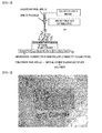
- FIG. 1 is a schematic view showing an electrospraying apparatus used to obtain a metal oxide nanoparticle thin layer in the method of manufacturing a gas sensor according to the present invention.
- the prepared solution is sprayed onto a substrate provided with a sensor electrode.
- the electrospraying apparatus includes a spray nozzle connected to a quantitative pump for quantitatively introducing the solution, a high voltage generator, a grounded conductive substrate, and the like.
- a sensor electrode is disposed on the grounded conductive substrate.
- the grounded conductive substrate is used as a negative electrode
- the spray nozzle provided with a pump that can adjust the amount of the solution discharged per hour is used as a positive electrode.
- a voltage of 8 ⁇ 30 kV is applied, the feed rate of the solution is adjusted to 10 ⁇ 100 ⁇ l/min, and then the solution is sprayed onto the conductive substrate provided with the sensor electrode until the thickness of a metal oxide nanoparticle thin layer is 0.1 ⁇ 10 ⁇ m.
- the method of manufacturing a gas sensor according to the present invention may further include the steps of primarily heat-treating the metal oxide nanoparticle thin layer (sensor material) at a temperature of 80 °C ⁇ 300 °C; and/or secondarily heat-treating the metal oxide nanoparticle thin layer (sensor material) at a temperature of 350 °C ⁇ 600°C.
- This heat treatment includes: a high-temperature drying process (primary heat treatment) that is carried out at a temperature of 80 °C ⁇ 300 °C in order to completely remove the solvent remaining on the substrate after spraying the solution; and a heat treatment process (secondary heat treatment) that is carried out at a temperature of 350 °C ⁇ 600 °C in order to increase the bonding force between metal oxide nanoparticles, to increase the adhesion between the metal oxide nanoparticle thin layer and the substrate and to improve the electrical characteristics of the metal oxide nanoparticle thin layer by the growth of the metal oxide nanoparticles.
- primary heat treatment that is carried out at a temperature of 80 °C ⁇ 300 °C in order to completely remove the solvent remaining on the substrate after spraying the solution
- secondary heat treatment that is carried out at a temperature of 350 °C ⁇ 600 °C in order to increase the bonding force between metal oxide nanoparticles, to increase the adhesion between the metal oxide nanoparticle thin layer and the substrate and to improve the electrical characteristics of the
- the primary heat treatment and/or the secondary heat treatment may be omitted when the metal oxide nanoparticle thin layer formed by spraying the solution has mechanical, electrical and thermal characteristics that are sufficiently stable.
- the method of manufacturing a gas sensor according to the present invention may further include the step of attaching the metal oxide nanoparticle thin layer (sensor material) to the substrate by thermal pressing.
- the pressure, temperature and time for which the thermal pressing is conducted may be appropriately selected in consideration of the characteristics of the used metal oxide nanoparticles.
- the thermal pressing may be conducted under the conditions of a temperature of 20 °C ⁇ 150 °C, a pressure of 0.01 MPa ⁇ 10 Mpa and a pressing time of 10 seconds ⁇ 10 minutes.
- Such thermal pressing serves to improve the adhesion between the metal oxide nanoparticle thin layer (sensor material) and the substrate and to improve the electrical and mechanical characteristics of the metal oxide nanoparticle thin layer.
- the thermal pressing may also be simultaneously conducted together with the above-mentioned heat treatment processes, that is, primary heat treatment that is carried out at a temperature of 80 °C ⁇ 300 °C in order to completely remove the solvent remaining on the substrate after spraying the solution and/or secondary heat treatment that is carried out at a temperature of 350°C ⁇ 600°C in order to increase the bonding force between metal oxide nanoparticles, to increase the adhesion between the metal oxide nanoparticle thin layer and the substrate and to improve the electrical characteristics of the metal oxide nanoparticle thin layer by growing the metal oxide nanoparticles.
- primary heat treatment that is carried out at a temperature of 80 °C ⁇ 300 °C in order to completely remove the solvent remaining on the substrate after spraying the solution
- secondary heat treatment that is carried out at a temperature of 350°C ⁇ 600°C in order to increase the bonding force between metal oxide nanoparticles, to increase the adhesion between the metal oxide nanoparticle thin layer and the substrate and to improve the electrical characteristics of the metal oxide nanoparticle thin
- ZnO zinc oxide
- Aldrich ⁇ 100 nm
- ethanol a solution for spray.
- ultrasonication was carried out for 30 minutes. Since the size of commercially-available zinc oxide nanoparticles is less than 100 nm, the solution for spray was prepared without performing a pulverizing process.
- the prepared solution was charged into a syringe, the syringe charged with the solution was mounted on an electrospraying apparatus, and then voltage was applied between a tip provided at the end of the syringe and a lower substrate to obtain a zinc oxide nanoparticle thin layer.
- the voltage was 12 Kv
- the flow rate of the solution was 30 ⁇ l/min
- the distance between the tip and the lower substrate was 10 cm.
- the zinc oxide nanoparticle thin layer formed on the sensor substrate in Example 1 was heat-treated (secondarily heat-treated) at a temperature of 500 °C.
- the heat treatment of the zinc oxide nanoparticle thin layer was carried out under an air atmosphere for 30 minutes using a box furnace.
- tin oxide (SnO 2 ) nanoparticles Aldrich, ⁇ 100 nm
- ethanol a solution for spray.
- ultrasonication was carried out for 30 minutes.
- the prepared solution for spray was charged into a syringe, the syringe charged with the solution was mounted on an electrospraying apparatus, and then voltage was applied between a tip provided at the end of the syringe and a lower substrate to obtain a tin oxide nanoparticle thin layer.
- the voltage was 12 Kv
- the flow rate of the solution was 30 ⁇ l/min
- the distance between the tip and the lower substrate was 10 cm.
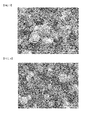
- FIG. 4 shows a scanning electron microscope photograph of the obtained tin oxide nanoparticle thin layer.
- the tin oxide nanoparticle thin layer is divided into two parts, that is, one part in which nanoparticles conglomerate with each other in a size of 300 ⁇ 1.5 ⁇ m and the other part in which nanoparticles are formed into a thin layer without conglomerating with each other. Further, it can be ascertained that, regardless of the conglomeration of nanoparticles during the spray process, all of the nanoparticle thin layers are composed of ultrafine tin oxide nanoparticles having a size of 20 ⁇ 100 nm.
- the tin oxide nanoparticle thin layer formed on the sensor substrate in Example 3 was heat-treated (secondarily heat-treated) at a temperature of 500°C.
- the heat treatment of the tin oxide nanoparticle thin layer was carried out under an air atmosphere for 30 minutes using a box furnace.
- FIG. 5 shows a scanning electron microscope (SEM) photograph of the tin oxide (SnO 2 ) nanoparticle thin layer prepared in Example 2, which has been heat-treated at 500°C.
- SEM scanning electron microscope
- the crystal growth of tin oxide nanoparticles occurs, and fine nanoparticles grow, so that the tin oxide nanoparticles are distributed in a size of 300 nm ⁇ 2 ⁇ m.
- the electroconductivity of the sensor material is improved because nanoparticles are more easily bonded with each other.
- the sensor material maintains a high specific surface area because the grown particles are also composed of fine nanoparticles.
- This heat treatment can improve the adhesive characteristics between the thin layer obtained by spraying at room temperature and the substrate provided with the sensor electrode.
- the heat treatment was carried out at a temperature of 500 °C, but is not limited to any specific temperature.
- the primary heat treatment in which the solution is dried at a temperature of 80 °C ⁇ 300 °C may be included in the second heat treatment.
- metal oxide nanoparticles in addition to the zinc oxide (ZnO) nanoparticles and tin oxide (SnO 2 ) nanoparticles, all kinds of metal oxide nanoparticles may be used as long as they are metal oxide nanoparticles having semiconductor characteristics.
- Specific examples of metal oxide nanoparticles may include SnO 2 , TiO 2 , ZnO, VO 2 , In 2 O 3 , NiO, MoO 3 , SrTiO 3 , Fe-doped SrTiO 3 , Fe 2 O 3 , WO 3 and CuO nanoparticles.
- Fe-doped SrTiO 3 When Fe-doped SrTiO 3 is used to manufacture an oxygen sensor, it may have a composition of SrTi 0.65 Fe 0.35 O 3 .
- the metal oxide nanoparticle thin layer formed by electrospraying can be used to manufacture a high sensitive sensor for detecting various environmental gases such as HC, H 2 , O 2 , CO, NOx, alcohol, NH 3 , CH 4 , SO x , DMMP, phenol, acetone, formaldehyde, VOCs (volatile organic compounds).
- environmental gases are not limited to specific gases as long as they are harmful environmental materials which can be detected by a change in resistance.
- Example 2 In order to evaluate the electrical characteristics of the zinc oxide (ZnO) nanoparticle thin layer (sensor material) obtained in Example 1, the current-voltage (I-V) characteristics thereof were evaluated using Agilent B 1500. The current change was measured while changing the applied voltage from -10V to +10V. Additionally, the current-voltage (I-V) characteristics of the heat-treated zinc oxide (ZnO) nanoparticle thin layer (sensor material) obtained in Example 2 were also evaluated.
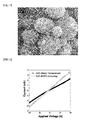
- FIG. 6 is a graph showing the current-voltage characteristics of the zinc oxide nanoparticle thin layer prepared in Example 1 and those of the zinc oxide nanoparticle thin layer (Example 2) which have additionally been heat-treated at 500 ⁇ .
- the current values of the thin layers are 2.5 ⁇ A and 4 ⁇ A (heat-treated ZnO thin layer) at an applied voltage of 10V, so that these thin layers exhibit typical semiconductor characteristics.
- FIG. 7 is a graph showing the current-voltage characteristics of the zinc oxide nanoparticle thin layers prepared in Examples 3 and 4.
- the current val ue of the tin oxide thin layer which has not been heat-treated is 2.5 nA at an applied voltage of 10V, so that this thin layer exhibited typical semiconductor characteristics.
- the current value of the tin oxide thin layer which was heat-treated (500°C) is 3000 ⁇ A at an applied voltage of 10V. Therefore, it can be ascertained that the electroconductivity of the tin oxide nanoparticle thin layer which has been heat-treated at 500 °C is greatly improved compared to that of the tin oxide nanoparticle thin layer which has not been heat-treated. The reason for this is because the contact characteristics between particles are improved by heat treatment.
- a gas sensor was manufactured using each of the tin oxide (SnO 2 ) nanoparticle thin layers prepared in Examples 3 and 4, and then the change in resistance before and after reaction at 300°C was measured using the gas sensor while changing carbon monoxide (CO) concentration.
- the gas sensor including the tin oxide nanoparticle thin layer was mounted in a quartz tube of a tube furnace.
- a Pt/Pt-Rh (type S) thermocouple measured temperature change while the gas sensor measured the change in resistance that occurred with various changes in a kind of gas and concentration of gas.
- Gas flow was controlled by MFC (Tylan UFC-1500A mass flow controller and Tylan RO-28 mass flow controller).
- the reaction was a reversible reaction, and the reaction time was very short. This measurement can also be carried out in a chamber provided with a heating element in addition to the tube furnace.
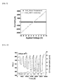
- FIG. 8 is a graph showing the results of measuring the change in resistance while changing the CO gas concentration from 0.5 ppm to 50 ppm at 300 °C, using the gas sensor manufactured using the tin oxide (SnO 2 ) nanoparticle thin layer.
- the gas sensor using the tin oxide (SnO 2 ) nanoparticle thin layer shows typical N-type semiconductor characteristics that the resistance decreases when the gas sensor is exposed to a reducing gas (CO).
- CO reducing gas
- the gas sensor can also easily measure a very small amount of CO (0.5 ppm) because it includes a tin oxide nanoparticle thin layer made of fine tine oxide nanoparticles.
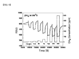
- the change in resistance before and after reaction at 300 °C was measured using the same sensor and method as those of Test example 3, except that the change in resistance thereof was measured while changing the CH 4 gas concentration from 7.5 ppm to 500 ppm at 300 °C.
- FIG. 9 is a graph showing the results of measuring the change in resistance while changing the CH 4 gas concentration from 7.5 ppm to 500 ppm at 300 °C, using the gas sensor manufactured using the tin oxide (SnO 2 ) nanoparticle thin layer.
- the gas sensor using the tin oxide (SnO 2 ) nanoparticle thin layer shows typical N-type semiconductor characteristics that the resistance decreases when the gas sensor is exposed to methane gas (CH 4 ).
- CH 4 methane gas
- metal oxide nanoparticles that can be used to obtain a thin layer (sensor material) for a gas sensor, and these are limited to specific metal oxide nanoparticles.
Landscapes
- Chemical & Material Sciences (AREA)
- Engineering & Computer Science (AREA)
- Chemical Kinetics & Catalysis (AREA)
- Organic Chemistry (AREA)
- Metallurgy (AREA)
- Mechanical Engineering (AREA)
- Materials Engineering (AREA)
- Health & Medical Sciences (AREA)
- Life Sciences & Earth Sciences (AREA)
- Physics & Mathematics (AREA)
- Immunology (AREA)
- Analytical Chemistry (AREA)
- General Health & Medical Sciences (AREA)
- Pathology (AREA)
- General Physics & Mathematics (AREA)
- Biochemistry (AREA)
- Nanotechnology (AREA)
- Electrochemistry (AREA)
- Medicinal Chemistry (AREA)
- Food Science & Technology (AREA)
- Combustion & Propulsion (AREA)
- Plasma & Fusion (AREA)
- Crystallography & Structural Chemistry (AREA)
- Manufacturing & Machinery (AREA)
- Investigating Or Analyzing Materials By The Use Of Fluid Adsorption Or Reactions (AREA)
Applications Claiming Priority (2)
| Application Number | Priority Date | Filing Date | Title |
|---|---|---|---|
| KR20090038043A KR101125170B1 (ko) | 2009-04-30 | 2009-04-30 | 금속산화물 나노입자를 이용한 가스센서 및 그 제조방법 |
| PCT/KR2010/002766 WO2010126336A2 (ko) | 2009-04-30 | 2010-04-30 | 금속산화물 나노입자를 이용한 가스센서 및 그 제조방법 |
Publications (3)
| Publication Number | Publication Date |
|---|---|
| EP2426484A2 true EP2426484A2 (de) | 2012-03-07 |
| EP2426484A4 EP2426484A4 (de) | 2015-12-02 |
| EP2426484B1 EP2426484B1 (de) | 2018-03-21 |
Family
ID=43032712
Family Applications (1)
| Application Number | Title | Priority Date | Filing Date |
|---|---|---|---|
| EP10769981.1A Active EP2426484B1 (de) | 2009-04-30 | 2010-04-30 | Verfahren zur herstellung eines gassensors mit metalloxidnanopartikeln |
Country Status (4)
| Country | Link |
|---|---|
| US (1) | US9133549B2 (de) |
| EP (1) | EP2426484B1 (de) |
| KR (1) | KR101125170B1 (de) |
| WO (1) | WO2010126336A2 (de) |
Cited By (5)
| Publication number | Priority date | Publication date | Assignee | Title |
|---|---|---|---|---|
| RU2509302C1 (ru) * | 2012-10-15 | 2014-03-10 | Федеральное государственное бюджетное образовательное учреждение высшего профессионального образования "Санкт-Петербургский государственный электротехнический университет "ЛЭТИ" им. В.И. Ульянова (Ленина)" | Способ получения газочувствительного материала на основе оксида цинка к парам ацетона |
| EP2837931A1 (de) * | 2013-08-16 | 2015-02-18 | Sensirion AG | Verfahren zur Herstellung eines integrierten Metalloxid-Gassensors |
| EP2837932A1 (de) * | 2013-08-16 | 2015-02-18 | Sensirion AG | Wärmebehandlungsverfahren für integrierte Metalloxid-Gassensoren |
| WO2017020859A1 (zh) * | 2015-08-06 | 2017-02-09 | 北京大学 | 锡掺杂的光催化甲醛传感材料及其制备方法和甲醛传感器 |
| EA034557B1 (ru) * | 2018-05-21 | 2020-02-20 | Федеральное государственное бюджетное образовательное учреждение высшего образования "Саратовский государственный технический университет имени Гагарина Ю.А." | Способ изготовления хеморезистора на основе наноструктур оксида цинка электрохимическим методом |
Families Citing this family (31)
| Publication number | Priority date | Publication date | Assignee | Title |
|---|---|---|---|---|
| US20140083508A1 (en) * | 2012-09-25 | 2014-03-27 | Research Foundation Of The City University Of New York | Method for forming an aluminum organic photovoltaic cell electrode and electrically conducting product thereof |
| KR101460500B1 (ko) * | 2013-02-27 | 2014-11-11 | 한양대학교 에리카산학협력단 | 칼코지나이드계 나노선을 이용한 열화학 가스 센서 및 그 제조방법 |
| KR102192973B1 (ko) * | 2013-12-19 | 2020-12-18 | 에스케이이노베이션 주식회사 | 나노 구조체를 갖는 센서 및 그 제조 방법 |
| DE102014203839A1 (de) * | 2014-03-03 | 2015-09-03 | Siemens Aktiengesellschaft | Verfahren zur Herstellung eines Gassensors |
| KR101618337B1 (ko) | 2014-04-18 | 2016-05-09 | 한국과학기술연구원 | 센서의 제조방법 및 이에 의하여 제조된 센서 |
| US10175227B2 (en) | 2015-05-20 | 2019-01-08 | Gm Nameplate, Inc. | Gas sensor module |
| US9897590B2 (en) | 2015-05-20 | 2018-02-20 | Gm Nameplate, Inc. | Breath capture and sampling system |
| EP3384280B1 (de) * | 2015-11-30 | 2023-10-11 | Robert Bosch GmbH | Umgebungssensorvorrichtung aus nanostrukturiertem nickeloxid und gehäuse zur verkapselung der vorrichtung |
| US10793964B2 (en) | 2016-05-04 | 2020-10-06 | Uchicago Argonne, Llc | Pre-treated functionalized multi-walled carbon nanotube based methane sensor |
| CN106568812B (zh) * | 2016-11-09 | 2020-03-17 | 西安交通大学 | 一种用于异戊二烯气体检测的气体传感器的制备方法 |
| KR101922187B1 (ko) * | 2017-03-13 | 2018-11-26 | 한국과학기술연구원 | 가스센서용 감지물질 및 그 제조방법, 그리고 상기 감지물질을 포함하는 가스센서 및 그 제조방법 |
| KR101990675B1 (ko) | 2017-03-22 | 2019-10-01 | 한양대학교 에리카산학협력단 | 가스 센서 및 그 제조 방법 |
| US11525818B2 (en) | 2018-01-05 | 2022-12-13 | King Fahd University Of Petroleum And Minerals | Hydrogen gas sensor and a method of fabricating thereof |
| US10942157B2 (en) | 2018-02-21 | 2021-03-09 | Stmicroelectronics Pte Ltd | Gas sensor device for detecting gases with large molecules |
| KR102090489B1 (ko) * | 2018-10-19 | 2020-03-18 | 한국과학기술연구원 | 산화구리 나노입자로 도핑된 그래핀을 이용한 암모니아 가스 검출 센서 및 이를 포함하는 암모니아 가스 검출 장치 |
| EP3705879A1 (de) * | 2019-03-06 | 2020-09-09 | Sensirion AG | Resistiver metalloxidgassensor |
| KR102301531B1 (ko) | 2019-06-11 | 2021-09-15 | 한국원자력연구원 | 그래핀 기반 가스 센서 및 그 제조 방법 |
| KR102352913B1 (ko) * | 2019-08-07 | 2022-01-19 | 한양대학교 산학협력단 | 가스센서용 금속/세라믹 복합체 및 그 제조 방법 |
| CN110672672A (zh) * | 2019-10-21 | 2020-01-10 | 陕西师范大学 | Zn–In2O3多孔纳米纤维气敏材料的制备方法及应用 |
| KR102236900B1 (ko) * | 2019-11-25 | 2021-04-06 | (주)라디안큐바이오 | 드롭 모드의 무전해 도금 방식을 이용한 금 나노구조체 제조 방법 |
| CN112323017B (zh) * | 2020-09-18 | 2022-10-04 | 中国科学院合肥物质科学研究院 | 一种氧化铜桥连纳米线器件及其制备方法和应用 |
| KR102462285B1 (ko) * | 2020-10-26 | 2022-11-03 | 한국전자기술연구원 | 잉크 조성물 및 그를 이용한 mems 기반 가스 센서의 제조 방법 |
| KR102567482B1 (ko) * | 2021-01-26 | 2023-08-17 | 한국과학기술연구원 | 산화주석 및 산화니켈 나노입자로 도핑된 그래핀을 이용한 고감도 암모니아 가스 검출 센서 및 암모니아 가스 검출 시스템의 개발 및 이의 제조 방법 |
| KR102487004B1 (ko) * | 2021-03-24 | 2023-01-11 | 울산대학교 산학협력단 | 니켈 산화물 용액 및 이를 이용한 열처리가 필요없는 태양전지의 제조 방법 |
| CN113325041B (zh) * | 2021-05-31 | 2022-10-04 | 吉林大学 | 基于金修饰富含氧空位二氧化锡的dmmp传感器及其制备方法 |
| CN113820363B (zh) * | 2021-08-27 | 2023-03-17 | 山东大学 | 铂负载的多孔氧化锡纳米球气敏材料及其制备方法与应用 |
| CN114622172B (zh) * | 2021-09-29 | 2023-12-01 | 天地(常州)自动化股份有限公司 | 氧化铝修饰的氧化锌气敏薄膜及其制备方法 |
| KR102622679B1 (ko) * | 2021-10-26 | 2024-01-10 | 한국전자기술연구원 | 자기조립단분자막을 이용한 가스 센서 및 그의 제조 방법 |
| CN113933360B (zh) * | 2021-11-22 | 2023-06-23 | 广州航海学院 | 一种用于提高氢气传感器性能的掺杂型敏感材料及其制备方法和应用 |
| KR102553980B1 (ko) * | 2022-11-16 | 2023-07-11 | 박준경 | 친환경 구리산화물 나노입자를 이용한 포름알데하이드 센서의 제조방법 |
| CN118961999B (zh) * | 2024-06-20 | 2025-09-16 | 中国科学院合肥物质科学研究院 | 一种可用于双模态检测多种VOCs的气体传感器及其制备方法 |
Family Cites Families (11)
| Publication number | Priority date | Publication date | Assignee | Title |
|---|---|---|---|---|
| GB9512929D0 (en) * | 1995-06-24 | 1995-08-30 | Sun Electric Uk Ltd | Multi-gas sensor systems for automatic emissions measurement |
| KR100583910B1 (ko) | 2003-07-02 | 2006-05-29 | 재단법인서울대학교산학협력재단 | 나노 입자의 정전 스프레이 방식을 이용한 나노 크기구조의 패터닝 방법 |
| US7259109B2 (en) | 2004-09-22 | 2007-08-21 | Intel Corporation | Electrospray and enhanced electrospray deposition of thin films on semiconductor substrates |
| EP1669747A1 (de) * | 2004-12-09 | 2006-06-14 | ETH Zürich | Bildung von hochporösen Schichten durch Abscheidung von durch Flammsprühpyrolyse hergestellten Nanopartikeln |
| KR100735031B1 (ko) * | 2004-12-22 | 2007-07-03 | 한국전자통신연구원 | 화학 센서 |
| KR100812357B1 (ko) * | 2005-12-23 | 2008-03-11 | 한국과학기술연구원 | 초고감도 금속산화물 가스센서 및 그 제조방법 |
| KR100843191B1 (ko) | 2006-03-30 | 2008-07-02 | 주식회사 아모메디 | 은 나노입자 함유 나노섬유 필터여재 및 그 제조방법 |
| KR20080052249A (ko) * | 2006-12-06 | 2008-06-11 | 한국전자통신연구원 | 금속산화물 반도체 화학센서 및 이의 제조 방법 |
| US7786037B2 (en) * | 2007-01-11 | 2010-08-31 | Los Alamos National Security, Llc | Nanostructured metal-polyaniline composites |
| KR100906496B1 (ko) * | 2007-07-27 | 2009-07-08 | (주)엠투엔 | 가스 센서 및 그 제조 방법 |
| KR101027074B1 (ko) | 2008-10-23 | 2011-04-05 | 서울대학교산학협력단 | 금속산화물층을 갖는 나노구조물 가스센서, 나노구조물 가스센서 어레이 및 그 제조 방법 |
-
2009
- 2009-04-30 KR KR20090038043A patent/KR101125170B1/ko active Active
-
2010
- 2010-04-30 EP EP10769981.1A patent/EP2426484B1/de active Active
- 2010-04-30 US US13/266,815 patent/US9133549B2/en active Active
- 2010-04-30 WO PCT/KR2010/002766 patent/WO2010126336A2/ko not_active Ceased
Non-Patent Citations (1)
| Title |
|---|
| See references of WO2010126336A2 * |
Cited By (5)
| Publication number | Priority date | Publication date | Assignee | Title |
|---|---|---|---|---|
| RU2509302C1 (ru) * | 2012-10-15 | 2014-03-10 | Федеральное государственное бюджетное образовательное учреждение высшего профессионального образования "Санкт-Петербургский государственный электротехнический университет "ЛЭТИ" им. В.И. Ульянова (Ленина)" | Способ получения газочувствительного материала на основе оксида цинка к парам ацетона |
| EP2837931A1 (de) * | 2013-08-16 | 2015-02-18 | Sensirion AG | Verfahren zur Herstellung eines integrierten Metalloxid-Gassensors |
| EP2837932A1 (de) * | 2013-08-16 | 2015-02-18 | Sensirion AG | Wärmebehandlungsverfahren für integrierte Metalloxid-Gassensoren |
| WO2017020859A1 (zh) * | 2015-08-06 | 2017-02-09 | 北京大学 | 锡掺杂的光催化甲醛传感材料及其制备方法和甲醛传感器 |
| EA034557B1 (ru) * | 2018-05-21 | 2020-02-20 | Федеральное государственное бюджетное образовательное учреждение высшего образования "Саратовский государственный технический университет имени Гагарина Ю.А." | Способ изготовления хеморезистора на основе наноструктур оксида цинка электрохимическим методом |
Also Published As
| Publication number | Publication date |
|---|---|
| WO2010126336A3 (ko) | 2011-01-27 |
| US9133549B2 (en) | 2015-09-15 |
| WO2010126336A2 (ko) | 2010-11-04 |
| KR20100119100A (ko) | 2010-11-09 |
| EP2426484A4 (de) | 2015-12-02 |
| EP2426484B1 (de) | 2018-03-21 |
| US20120042713A1 (en) | 2012-02-23 |
| KR101125170B1 (ko) | 2012-03-19 |
Similar Documents
| Publication | Publication Date | Title |
|---|---|---|
| US9133549B2 (en) | Gas sensor using metal oxide nanoparticles, and method for manufacturing same | |
| JP4523582B2 (ja) | 金属酸化物ガスセンサの製造方法 | |
| KR101035003B1 (ko) | 촉매를 포함하는 금속산화물 가스센서 및 이의 제조방법 | |
| CN104569061B (zh) | 金属氧化物半导体气体传感器及其制备方法 | |
| Jiménez-Cadena et al. | Gas sensors based on nanostructured materials | |
| Ayesh | Metal/Metal‐Oxide Nanoclusters for Gas Sensor Applications | |
| US10845325B2 (en) | In-situ localized growth of porous metal oxide films on microheater platform for low temperature gas detection | |
| KR20100071618A (ko) | 센서용 산화물 반도체 나노섬유 제조 방법 및 그를 이용한 가스 센서 | |
| EP2220482B1 (de) | Gassensor mit einer verbesserten selektivität | |
| WO2008153593A1 (en) | Nanomaterial-based gas sensors | |
| KR101859832B1 (ko) | 광소결을 통한 상변화 및 입성장 된 3차원 나노계층구조 금속산화물 감지층을 이용한 가스 센서용 부재, 가스 센서 및 그 제조 방법 | |
| CN204389426U (zh) | 金属氧化物半导体气体传感器 | |
| KR101201896B1 (ko) | 정전용량형 환경유해가스 센서 및 그 제조방법 | |
| KR102643736B1 (ko) | 금속화합물-다층 그래핀으로 이루어진 핵-껍질 양자점을 포함하는 가스 센서 및 그 제조방법 | |
| KR101552326B1 (ko) | 금속산화물 반도체 나노섬유와 이중 촉매를 이용한 가스 센서용 부재 및 그 제조 방법 | |
| EA036464B1 (ru) | Мультиоксидное газоаналитическое устройство и способ его изготовления | |
| Kruefu et al. | Selectivity of flame-spray-made Nb/ZnO thick films towards NO2 gas | |
| Hussain et al. | Oxygen sensing and transport properties of nanofibers of silica, bismuth doped silica and bismuth silicate prepared via electrospinning | |
| WO2008014153A1 (en) | Sensors for detecting nox in a gas and methods for fabricating the same | |
| KR20130112531A (ko) | 복합 계층 구조를 갖는 가스 감지막, 이를 포함하는 가스센서 및 그 제조 방법 | |
| Li et al. | Fabrication and characterization of a low power consumption ethanol gas sensor based on a suspended micro-hotplate | |
| Hunter et al. | Chemical sensors based on metal oxide nanostructures | |
| EP4660621A1 (de) | Metalloxid-halbleiter-gassensor | |
| KR102389583B1 (ko) | 1차원 다공성 이종금속 나노벨트, 이를 이용한 가스센서 및 가스센서 제조 방법 | |
| Chang et al. | La-doped SnO2/ZnO brush-distributed nanostructure for enhancing ethanol sensing performance |
Legal Events
| Date | Code | Title | Description |
|---|---|---|---|
| PUAI | Public reference made under article 153(3) epc to a published international application that has entered the european phase |
Free format text: ORIGINAL CODE: 0009012 |
|
| 17P | Request for examination filed |
Effective date: 20111129 |
|
| AK | Designated contracting states |
Kind code of ref document: A2 Designated state(s): AT BE BG CH CY CZ DE DK EE ES FI FR GB GR HR HU IE IS IT LI LT LU LV MC MK MT NL NO PL PT RO SE SI SK SM TR |
|
| DAX | Request for extension of the european patent (deleted) | ||
| REG | Reference to a national code |
Ref country code: DE Ref legal event code: R079 Ref document number: 602010049326 Country of ref document: DE Free format text: PREVIOUS MAIN CLASS: G01N0027120000 Ipc: C23C0024020000 |
|
| A4 | Supplementary search report drawn up and despatched |
Effective date: 20151029 |
|
| RIC1 | Information provided on ipc code assigned before grant |
Ipc: C23C 24/02 20060101AFI20151023BHEP Ipc: G01N 27/12 20060101ALI20151023BHEP Ipc: G01N 33/00 20060101ALI20151023BHEP Ipc: B05B 5/025 20060101ALI20151023BHEP |
|
| GRAP | Despatch of communication of intention to grant a patent |
Free format text: ORIGINAL CODE: EPIDOSNIGR1 |
|
| INTG | Intention to grant announced |
Effective date: 20171123 |
|
| GRAS | Grant fee paid |
Free format text: ORIGINAL CODE: EPIDOSNIGR3 |
|
| GRAA | (expected) grant |
Free format text: ORIGINAL CODE: 0009210 |
|
| AK | Designated contracting states |
Kind code of ref document: B1 Designated state(s): AT BE BG CH CY CZ DE DK EE ES FI FR GB GR HR HU IE IS IT LI LT LU LV MC MK MT NL NO PL PT RO SE SI SK SM TR |
|
| REG | Reference to a national code |
Ref country code: GB Ref legal event code: FG4D |
|
| REG | Reference to a national code |
Ref country code: CH Ref legal event code: EP |
|
| REG | Reference to a national code |
Ref country code: AT Ref legal event code: REF Ref document number: 981190 Country of ref document: AT Kind code of ref document: T Effective date: 20180415 |
|
| REG | Reference to a national code |
Ref country code: IE Ref legal event code: FG4D |
|
| REG | Reference to a national code |
Ref country code: DE Ref legal event code: R096 Ref document number: 602010049326 Country of ref document: DE |
|
| REG | Reference to a national code |
Ref country code: FR Ref legal event code: PLFP Year of fee payment: 9 |
|
| REG | Reference to a national code |
Ref country code: NL Ref legal event code: MP Effective date: 20180321 |
|
| PG25 | Lapsed in a contracting state [announced via postgrant information from national office to epo] |
Ref country code: FI Free format text: LAPSE BECAUSE OF FAILURE TO SUBMIT A TRANSLATION OF THE DESCRIPTION OR TO PAY THE FEE WITHIN THE PRESCRIBED TIME-LIMIT Effective date: 20180321 Ref country code: CY Free format text: LAPSE BECAUSE OF FAILURE TO SUBMIT A TRANSLATION OF THE DESCRIPTION OR TO PAY THE FEE WITHIN THE PRESCRIBED TIME-LIMIT Effective date: 20180321 Ref country code: LT Free format text: LAPSE BECAUSE OF FAILURE TO SUBMIT A TRANSLATION OF THE DESCRIPTION OR TO PAY THE FEE WITHIN THE PRESCRIBED TIME-LIMIT Effective date: 20180321 Ref country code: NO Free format text: LAPSE BECAUSE OF FAILURE TO SUBMIT A TRANSLATION OF THE DESCRIPTION OR TO PAY THE FEE WITHIN THE PRESCRIBED TIME-LIMIT Effective date: 20180621 Ref country code: HR Free format text: LAPSE BECAUSE OF FAILURE TO SUBMIT A TRANSLATION OF THE DESCRIPTION OR TO PAY THE FEE WITHIN THE PRESCRIBED TIME-LIMIT Effective date: 20180321 |
|
| REG | Reference to a national code |
Ref country code: LT Ref legal event code: MG4D |
|
| REG | Reference to a national code |
Ref country code: AT Ref legal event code: MK05 Ref document number: 981190 Country of ref document: AT Kind code of ref document: T Effective date: 20180321 |
|
| PG25 | Lapsed in a contracting state [announced via postgrant information from national office to epo] |
Ref country code: GR Free format text: LAPSE BECAUSE OF FAILURE TO SUBMIT A TRANSLATION OF THE DESCRIPTION OR TO PAY THE FEE WITHIN THE PRESCRIBED TIME-LIMIT Effective date: 20180622 Ref country code: BG Free format text: LAPSE BECAUSE OF FAILURE TO SUBMIT A TRANSLATION OF THE DESCRIPTION OR TO PAY THE FEE WITHIN THE PRESCRIBED TIME-LIMIT Effective date: 20180621 Ref country code: SE Free format text: LAPSE BECAUSE OF FAILURE TO SUBMIT A TRANSLATION OF THE DESCRIPTION OR TO PAY THE FEE WITHIN THE PRESCRIBED TIME-LIMIT Effective date: 20180321 Ref country code: LV Free format text: LAPSE BECAUSE OF FAILURE TO SUBMIT A TRANSLATION OF THE DESCRIPTION OR TO PAY THE FEE WITHIN THE PRESCRIBED TIME-LIMIT Effective date: 20180321 |
|
| PG25 | Lapsed in a contracting state [announced via postgrant information from national office to epo] |
Ref country code: PL Free format text: LAPSE BECAUSE OF FAILURE TO SUBMIT A TRANSLATION OF THE DESCRIPTION OR TO PAY THE FEE WITHIN THE PRESCRIBED TIME-LIMIT Effective date: 20180321 Ref country code: EE Free format text: LAPSE BECAUSE OF FAILURE TO SUBMIT A TRANSLATION OF THE DESCRIPTION OR TO PAY THE FEE WITHIN THE PRESCRIBED TIME-LIMIT Effective date: 20180321 Ref country code: NL Free format text: LAPSE BECAUSE OF FAILURE TO SUBMIT A TRANSLATION OF THE DESCRIPTION OR TO PAY THE FEE WITHIN THE PRESCRIBED TIME-LIMIT Effective date: 20180321 Ref country code: ES Free format text: LAPSE BECAUSE OF FAILURE TO SUBMIT A TRANSLATION OF THE DESCRIPTION OR TO PAY THE FEE WITHIN THE PRESCRIBED TIME-LIMIT Effective date: 20180321 Ref country code: RO Free format text: LAPSE BECAUSE OF FAILURE TO SUBMIT A TRANSLATION OF THE DESCRIPTION OR TO PAY THE FEE WITHIN THE PRESCRIBED TIME-LIMIT Effective date: 20180321 Ref country code: IT Free format text: LAPSE BECAUSE OF FAILURE TO SUBMIT A TRANSLATION OF THE DESCRIPTION OR TO PAY THE FEE WITHIN THE PRESCRIBED TIME-LIMIT Effective date: 20180321 |
|
| PG25 | Lapsed in a contracting state [announced via postgrant information from national office to epo] |
Ref country code: CZ Free format text: LAPSE BECAUSE OF FAILURE TO SUBMIT A TRANSLATION OF THE DESCRIPTION OR TO PAY THE FEE WITHIN THE PRESCRIBED TIME-LIMIT Effective date: 20180321 Ref country code: AT Free format text: LAPSE BECAUSE OF FAILURE TO SUBMIT A TRANSLATION OF THE DESCRIPTION OR TO PAY THE FEE WITHIN THE PRESCRIBED TIME-LIMIT Effective date: 20180321 Ref country code: SM Free format text: LAPSE BECAUSE OF FAILURE TO SUBMIT A TRANSLATION OF THE DESCRIPTION OR TO PAY THE FEE WITHIN THE PRESCRIBED TIME-LIMIT Effective date: 20180321 Ref country code: SK Free format text: LAPSE BECAUSE OF FAILURE TO SUBMIT A TRANSLATION OF THE DESCRIPTION OR TO PAY THE FEE WITHIN THE PRESCRIBED TIME-LIMIT Effective date: 20180321 |
|
| REG | Reference to a national code |
Ref country code: CH Ref legal event code: PL |
|
| REG | Reference to a national code |
Ref country code: BE Ref legal event code: MM Effective date: 20180430 |
|
| PG25 | Lapsed in a contracting state [announced via postgrant information from national office to epo] |
Ref country code: PT Free format text: LAPSE BECAUSE OF FAILURE TO SUBMIT A TRANSLATION OF THE DESCRIPTION OR TO PAY THE FEE WITHIN THE PRESCRIBED TIME-LIMIT Effective date: 20180723 |
|
| REG | Reference to a national code |
Ref country code: DE Ref legal event code: R097 Ref document number: 602010049326 Country of ref document: DE |
|
| REG | Reference to a national code |
Ref country code: IE Ref legal event code: MM4A |
|
| PLBE | No opposition filed within time limit |
Free format text: ORIGINAL CODE: 0009261 |
|
| STAA | Information on the status of an ep patent application or granted ep patent |
Free format text: STATUS: NO OPPOSITION FILED WITHIN TIME LIMIT |
|
| PG25 | Lapsed in a contracting state [announced via postgrant information from national office to epo] |
Ref country code: DK Free format text: LAPSE BECAUSE OF FAILURE TO SUBMIT A TRANSLATION OF THE DESCRIPTION OR TO PAY THE FEE WITHIN THE PRESCRIBED TIME-LIMIT Effective date: 20180321 Ref country code: MC Free format text: LAPSE BECAUSE OF FAILURE TO SUBMIT A TRANSLATION OF THE DESCRIPTION OR TO PAY THE FEE WITHIN THE PRESCRIBED TIME-LIMIT Effective date: 20180321 Ref country code: LU Free format text: LAPSE BECAUSE OF NON-PAYMENT OF DUE FEES Effective date: 20180430 |
|
| 26N | No opposition filed |
Effective date: 20190102 |
|
| PG25 | Lapsed in a contracting state [announced via postgrant information from national office to epo] |
Ref country code: LI Free format text: LAPSE BECAUSE OF NON-PAYMENT OF DUE FEES Effective date: 20180430 Ref country code: CH Free format text: LAPSE BECAUSE OF NON-PAYMENT OF DUE FEES Effective date: 20180430 Ref country code: BE Free format text: LAPSE BECAUSE OF NON-PAYMENT OF DUE FEES Effective date: 20180430 |
|
| PG25 | Lapsed in a contracting state [announced via postgrant information from national office to epo] |
Ref country code: IE Free format text: LAPSE BECAUSE OF NON-PAYMENT OF DUE FEES Effective date: 20180430 |
|
| PG25 | Lapsed in a contracting state [announced via postgrant information from national office to epo] |
Ref country code: SI Free format text: LAPSE BECAUSE OF FAILURE TO SUBMIT A TRANSLATION OF THE DESCRIPTION OR TO PAY THE FEE WITHIN THE PRESCRIBED TIME-LIMIT Effective date: 20180321 |
|
| PG25 | Lapsed in a contracting state [announced via postgrant information from national office to epo] |
Ref country code: MT Free format text: LAPSE BECAUSE OF NON-PAYMENT OF DUE FEES Effective date: 20180430 |
|
| PG25 | Lapsed in a contracting state [announced via postgrant information from national office to epo] |
Ref country code: TR Free format text: LAPSE BECAUSE OF FAILURE TO SUBMIT A TRANSLATION OF THE DESCRIPTION OR TO PAY THE FEE WITHIN THE PRESCRIBED TIME-LIMIT Effective date: 20180321 |
|
| PG25 | Lapsed in a contracting state [announced via postgrant information from national office to epo] |
Ref country code: HU Free format text: LAPSE BECAUSE OF FAILURE TO SUBMIT A TRANSLATION OF THE DESCRIPTION OR TO PAY THE FEE WITHIN THE PRESCRIBED TIME-LIMIT; INVALID AB INITIO Effective date: 20100430 |
|
| PG25 | Lapsed in a contracting state [announced via postgrant information from national office to epo] |
Ref country code: MK Free format text: LAPSE BECAUSE OF NON-PAYMENT OF DUE FEES Effective date: 20180321 |
|
| PG25 | Lapsed in a contracting state [announced via postgrant information from national office to epo] |
Ref country code: IS Free format text: LAPSE BECAUSE OF FAILURE TO SUBMIT A TRANSLATION OF THE DESCRIPTION OR TO PAY THE FEE WITHIN THE PRESCRIBED TIME-LIMIT Effective date: 20180721 |
|
| PGFP | Annual fee paid to national office [announced via postgrant information from national office to epo] |
Ref country code: DE Payment date: 20250320 Year of fee payment: 16 |
|
| PGFP | Annual fee paid to national office [announced via postgrant information from national office to epo] |
Ref country code: GB Payment date: 20260324 Year of fee payment: 17 |
|
| PGFP | Annual fee paid to national office [announced via postgrant information from national office to epo] |
Ref country code: FR Payment date: 20260323 Year of fee payment: 17 |