EP2410582B1 - Diode électroluminescente à nano-bâtonnets et procédé de fabrication d'une diode électroluminescente à nano-bâtonnets - Google Patents
Diode électroluminescente à nano-bâtonnets et procédé de fabrication d'une diode électroluminescente à nano-bâtonnets Download PDFInfo
- Publication number
- EP2410582B1 EP2410582B1 EP11186011.0A EP11186011A EP2410582B1 EP 2410582 B1 EP2410582 B1 EP 2410582B1 EP 11186011 A EP11186011 A EP 11186011A EP 2410582 B1 EP2410582 B1 EP 2410582B1
- Authority
- EP
- European Patent Office
- Prior art keywords
- nano
- light emitting
- nano rod
- layer
- polarity
- Prior art date
- Legal status (The legal status is an assumption and is not a legal conclusion. Google has not performed a legal analysis and makes no representation as to the accuracy of the status listed.)
- Active
Links
Images


Classifications
-
- H—ELECTRICITY
- H01—ELECTRIC ELEMENTS
- H01L—SEMICONDUCTOR DEVICES NOT COVERED BY CLASS H10
- H01L33/00—Semiconductor devices with at least one potential-jump barrier or surface barrier specially adapted for light emission; Processes or apparatus specially adapted for the manufacture or treatment thereof or of parts thereof; Details thereof
- H01L33/02—Semiconductor devices with at least one potential-jump barrier or surface barrier specially adapted for light emission; Processes or apparatus specially adapted for the manufacture or treatment thereof or of parts thereof; Details thereof characterised by the semiconductor bodies
- H01L33/16—Semiconductor devices with at least one potential-jump barrier or surface barrier specially adapted for light emission; Processes or apparatus specially adapted for the manufacture or treatment thereof or of parts thereof; Details thereof characterised by the semiconductor bodies with a particular crystal structure or orientation, e.g. polycrystalline, amorphous or porous
- H01L33/18—Semiconductor devices with at least one potential-jump barrier or surface barrier specially adapted for light emission; Processes or apparatus specially adapted for the manufacture or treatment thereof or of parts thereof; Details thereof characterised by the semiconductor bodies with a particular crystal structure or orientation, e.g. polycrystalline, amorphous or porous within the light emitting region
-
- H—ELECTRICITY
- H01—ELECTRIC ELEMENTS
- H01L—SEMICONDUCTOR DEVICES NOT COVERED BY CLASS H10
- H01L33/00—Semiconductor devices with at least one potential-jump barrier or surface barrier specially adapted for light emission; Processes or apparatus specially adapted for the manufacture or treatment thereof or of parts thereof; Details thereof
- H01L33/005—Processes
- H01L33/0093—Wafer bonding; Removal of the growth substrate
-
- B—PERFORMING OPERATIONS; TRANSPORTING
- B82—NANOTECHNOLOGY
- B82Y—SPECIFIC USES OR APPLICATIONS OF NANOSTRUCTURES; MEASUREMENT OR ANALYSIS OF NANOSTRUCTURES; MANUFACTURE OR TREATMENT OF NANOSTRUCTURES
- B82Y20/00—Nanooptics, e.g. quantum optics or photonic crystals
-
- H—ELECTRICITY
- H01—ELECTRIC ELEMENTS
- H01L—SEMICONDUCTOR DEVICES NOT COVERED BY CLASS H10
- H01L33/00—Semiconductor devices with at least one potential-jump barrier or surface barrier specially adapted for light emission; Processes or apparatus specially adapted for the manufacture or treatment thereof or of parts thereof; Details thereof
- H01L33/005—Processes
- H01L33/0062—Processes for devices with an active region comprising only III-V compounds
- H01L33/0066—Processes for devices with an active region comprising only III-V compounds with a substrate not being a III-V compound
- H01L33/007—Processes for devices with an active region comprising only III-V compounds with a substrate not being a III-V compound comprising nitride compounds
-
- H—ELECTRICITY
- H01—ELECTRIC ELEMENTS
- H01L—SEMICONDUCTOR DEVICES NOT COVERED BY CLASS H10
- H01L33/00—Semiconductor devices with at least one potential-jump barrier or surface barrier specially adapted for light emission; Processes or apparatus specially adapted for the manufacture or treatment thereof or of parts thereof; Details thereof
- H01L33/02—Semiconductor devices with at least one potential-jump barrier or surface barrier specially adapted for light emission; Processes or apparatus specially adapted for the manufacture or treatment thereof or of parts thereof; Details thereof characterised by the semiconductor bodies
- H01L33/08—Semiconductor devices with at least one potential-jump barrier or surface barrier specially adapted for light emission; Processes or apparatus specially adapted for the manufacture or treatment thereof or of parts thereof; Details thereof characterised by the semiconductor bodies with a plurality of light emitting regions, e.g. laterally discontinuous light emitting layer or photoluminescent region integrated within the semiconductor body
-
- H—ELECTRICITY
- H01—ELECTRIC ELEMENTS
- H01L—SEMICONDUCTOR DEVICES NOT COVERED BY CLASS H10
- H01L33/00—Semiconductor devices with at least one potential-jump barrier or surface barrier specially adapted for light emission; Processes or apparatus specially adapted for the manufacture or treatment thereof or of parts thereof; Details thereof
- H01L33/02—Semiconductor devices with at least one potential-jump barrier or surface barrier specially adapted for light emission; Processes or apparatus specially adapted for the manufacture or treatment thereof or of parts thereof; Details thereof characterised by the semiconductor bodies
- H01L33/20—Semiconductor devices with at least one potential-jump barrier or surface barrier specially adapted for light emission; Processes or apparatus specially adapted for the manufacture or treatment thereof or of parts thereof; Details thereof characterised by the semiconductor bodies with a particular shape, e.g. curved or truncated substrate
- H01L33/24—Semiconductor devices with at least one potential-jump barrier or surface barrier specially adapted for light emission; Processes or apparatus specially adapted for the manufacture or treatment thereof or of parts thereof; Details thereof characterised by the semiconductor bodies with a particular shape, e.g. curved or truncated substrate of the light emitting region, e.g. non-planar junction
-
- H—ELECTRICITY
- H01—ELECTRIC ELEMENTS
- H01L—SEMICONDUCTOR DEVICES NOT COVERED BY CLASS H10
- H01L33/00—Semiconductor devices with at least one potential-jump barrier or surface barrier specially adapted for light emission; Processes or apparatus specially adapted for the manufacture or treatment thereof or of parts thereof; Details thereof
- H01L33/02—Semiconductor devices with at least one potential-jump barrier or surface barrier specially adapted for light emission; Processes or apparatus specially adapted for the manufacture or treatment thereof or of parts thereof; Details thereof characterised by the semiconductor bodies
- H01L33/26—Materials of the light emitting region
- H01L33/28—Materials of the light emitting region containing only elements of group II and group VI of the periodic system
-
- H—ELECTRICITY
- H01—ELECTRIC ELEMENTS
- H01L—SEMICONDUCTOR DEVICES NOT COVERED BY CLASS H10
- H01L33/00—Semiconductor devices with at least one potential-jump barrier or surface barrier specially adapted for light emission; Processes or apparatus specially adapted for the manufacture or treatment thereof or of parts thereof; Details thereof
- H01L33/02—Semiconductor devices with at least one potential-jump barrier or surface barrier specially adapted for light emission; Processes or apparatus specially adapted for the manufacture or treatment thereof or of parts thereof; Details thereof characterised by the semiconductor bodies
- H01L33/26—Materials of the light emitting region
- H01L33/30—Materials of the light emitting region containing only elements of group III and group V of the periodic system
- H01L33/32—Materials of the light emitting region containing only elements of group III and group V of the periodic system containing nitrogen
-
- H—ELECTRICITY
- H01—ELECTRIC ELEMENTS
- H01L—SEMICONDUCTOR DEVICES NOT COVERED BY CLASS H10
- H01L33/00—Semiconductor devices with at least one potential-jump barrier or surface barrier specially adapted for light emission; Processes or apparatus specially adapted for the manufacture or treatment thereof or of parts thereof; Details thereof
- H01L33/36—Semiconductor devices with at least one potential-jump barrier or surface barrier specially adapted for light emission; Processes or apparatus specially adapted for the manufacture or treatment thereof or of parts thereof; Details thereof characterised by the electrodes
- H01L33/40—Materials therefor
- H01L33/405—Reflective materials
-
- H—ELECTRICITY
- H01—ELECTRIC ELEMENTS
- H01L—SEMICONDUCTOR DEVICES NOT COVERED BY CLASS H10
- H01L33/00—Semiconductor devices with at least one potential-jump barrier or surface barrier specially adapted for light emission; Processes or apparatus specially adapted for the manufacture or treatment thereof or of parts thereof; Details thereof
- H01L33/36—Semiconductor devices with at least one potential-jump barrier or surface barrier specially adapted for light emission; Processes or apparatus specially adapted for the manufacture or treatment thereof or of parts thereof; Details thereof characterised by the electrodes
- H01L33/40—Materials therefor
- H01L33/42—Transparent materials
-
- Y—GENERAL TAGGING OF NEW TECHNOLOGICAL DEVELOPMENTS; GENERAL TAGGING OF CROSS-SECTIONAL TECHNOLOGIES SPANNING OVER SEVERAL SECTIONS OF THE IPC; TECHNICAL SUBJECTS COVERED BY FORMER USPC CROSS-REFERENCE ART COLLECTIONS [XRACs] AND DIGESTS
- Y10—TECHNICAL SUBJECTS COVERED BY FORMER USPC
- Y10S—TECHNICAL SUBJECTS COVERED BY FORMER USPC CROSS-REFERENCE ART COLLECTIONS [XRACs] AND DIGESTS
- Y10S977/00—Nanotechnology
- Y10S977/902—Specified use of nanostructure
- Y10S977/932—Specified use of nanostructure for electronic or optoelectronic application
- Y10S977/949—Radiation emitter using nanostructure
- Y10S977/95—Electromagnetic energy
Definitions
- the present invention relates to a nano rod type light emitting diode (LED) and a method for fabricating a nano rod type LED.
- LED light emitting diode
- a light emitting diode is a light source with a single wavelength, which has various applications such as light sources for cars, electronic display boards, lighting devices, and backlight units for display devices.
- Light generated in a light emitting diode is mostly confined inside the diode due to total internal reflection with a critical angle at an interface between two media such as a semiconductor and air.
- FIG. 1 is a conceptual diagram illustrating a light path between two media having different refraction indices.
- the light follows the Snell's law that is expressed by Equation 1. That is, light incident on the second medium from the first medium with an angle less than the critical angle passes through an interface in-between and light incident at an angle larger than the critical angle undergoes a total internal reflection.
- n 1 * sin ⁇ 1 n 2 * sin ⁇ 2
- ⁇ 1 is an incident angle and ⁇ 2 is a refraction angle.
- FIG. 2 is a schematic sectional view showing a light path in a typical light emitting diode.
- a light emitting diode in which an n-semiconductor layer (11), an active layer (12) and a p-semiconductor layer (13) are laminated in sequence on a substrate (10), light (a, b, c) traveling to the outside of the device at an angle less than a critical angle among light emitted from the active layer (12) passes through an interface.
- the light output of the light emitting diode decreases and the characteristics thereof are degraded.
- the surface texturing techniques are for improving light extraction efficiency in a light emitting diode chip. They can further improve the light extraction efficiency by being employed in combination with other existing techniques such as a chip shape modification technique, an epoxy encapsulation technique, and a substrate modification technique.
- the surface texturing techniques currently employ a method for providing a texture on a surface by forming a pattern using a mask or the like and performing wet or dry etching.
- each layer in the structure of a light emitting diode has a certain thickness and thus the height of a surface texture is restricted.
- etching thickness needs to be precisely controlled and reproduced during the etching process.
- the n-GaN nanocolumns and InGaN/GaN MQD active regions have isolated columnar structures, while the column-diameters gradually increase in the p-GaN region by controlling the growth conditions. Consequently, the resulting nanocolumn LED has a continuous top surface without chasms.
- This LED structure enables p-type electrodes to be fabricated by a conventional method on top of such nanocolumn LEDs while keeping the superior light-emitting properties of the laterally isolated nanocolumn active region.
- the resulting nanocolumn LED shows clear rectifying behavior with a typical turn-on voltage of 2.5 - 3.0 V at room temperature. Electroluminescence is observed through semitransparent electrodes with various emission colors from green (530 nm) to red (645 nm).
- the present invention is conceived to solve the aforementioned problems in the prior art.
- the present invention provides a nano rod type light emitting diode (LED) in accordance with the appended claim 1.
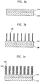
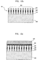
- FIGS. 3a to 3c are sectional views illustrating processes of fabricating a light emitting device with rods according to an illustrative example which does not form part of the present invention as defined by the claims but illustrates its context.
- a first polarity (i.e. conductivity-type) layer (110) is levelly formed on a substrate (100) ( FIG. 3a ).
- a plurality of light emitting rods (120) are formed on the first polarity layer (110) such that they are spaced apart from one another ( FIG. 3b ).
- a second polarity (i.e. conductivity-type) layer (130) is formed to wrap around each of the plurality of rods (120) ( FIG. 3c ).
- first polarity layer (110) and the second polarity layer (130) are defined as having opposite polarities.
- the second polarity layer (130) is a p-type semiconductor layer.
- the first polarity layer (110) is an n-type, it is an electron-supplying layer. If the second polarity layer (130) is a p-type, it is a hole-supplying layer.
- the polarities of the first and second polarity layers (110, 130) can be designed arbitrarily.
- the plurality of rods (120) correspond to active layers capable of emitting light.
- the rod type light emitting device comprises the first polarity layer (110), the plurality of light emitting rods (120) formed on the first polarity layer (110) such that they are spaced apart from one another, and the second polarity layer (130) wrapping around each of the plurality of rods (120).
- the substrate (100) is preferably provided below the first polarity layer (110).
- the plurality of rods (120) be ultra-minute structures having a width on the order of nanometres.
- FIG. 4 is a sectional view showing a state where light is emitted from the rod type light emitting device according to the illustrative example. Since the plurality of rods (120) are active layers capable of emitting light, each of the rods (120) emits light over an entire surface thereof. Thus, a light emitting area is increased to improve the light output of the device.
- the plurality of rods (120) spaced apart from one another emit light, the amount of light emitted to the outside without being confined within the device is increased. Thus, total internal reflection occurring in a conventional device is not a concern in the context of the present invention.
- FIG. 5 is a sectional view showing a vertical structure of the rod type light emitting device according to the example illustrating the context of the present invention. If the substrate (100) illustrated in FIG. 3c is a conductive substrate, an electrode (140) is formed on the rods (120).
- FIG. 6 is a sectional view showing a horizontal structure of the rod type light emitting device according to the example illustrating the context of the present invention. If the substrate (100) in FIG. 3c is a non-conductive substrate, the plurality of rods (120) are formed only on a part of the first polarity layer (110).
- electrodes (140, 150) are formed on the rods (120) and a part of the first polarity layer where a rod is not formed, respectively.
- FIGS. 7a and 7b are sectional views showing a state where a conductive material is filled between the rods of the rod type light emitting device according to the example illustrating the context of the present invention.
- the conductive material (160) is filled between the second polarity layers (130) wrapping around the rods (120).
- the conductive material (160) can facilitate the supply of an electric current to the rods (120).
- the conductive material (160) is preferably a transparent conductive material in a sol-gel state. It is preferred that the transparent conductive material be one of ITO, IZO, ZnO and AZO.
- FIGS. 8a and 8b are views showing second polarity layers protruding beyond a conductive material film according to the illustrative example and illustrating a light extraction path.
- the conductive material (160) is filled between the second polarity layers (130) wrapping around the rods (120) in such a manner that the second polarity layers (130) partially protrude beyond the conductive material (160).
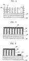
- FIG. 9 is a sectional view showing another structure of the rod type light emitting device according to an illustrative example. As described above, the plurality of rods (120) are formed on the first polarity layer (110).
- each of the rods (120) is wrapped sequentially by a second polarity layer (130), a current transport enhanced layer (CTEL) (200) and a transparent conductive oxide film (210), thereby forming the rod type emitting device according to the example illustrating the context of the present invention.
- CEL current transport enhanced layer
- the current transport enhanced layer (200) contains the material of the second polarity layer (130) and thus improves carrier mobility to facilitate the flow of an electric current.
- the current transport enhanced layer (200) is formed of a material containing GaN.
- the current transport enhanced layer (200) is defined as a layer formed of a material of which a work function is smaller than that of the second polarity layer (130) and larger than that of the transparent conductive oxide film (150).
- FIGS. 10a and 10b When the current transport enhanced layer (CTEL) and the transparent conductive oxide film are sequentially wrapped on the p-GaN layer, an energy band diagram at interfaces is shown in FIG. 10a .
- CTEL current transport enhanced layer
- FIG. 10a An energy band diagram at interfaces is shown in FIG. 10a .
- the deposited transparent conductive oxide film is not in ohmic contact with the current transport enhanced layer.
- the Schottky barrier is lowered to establish ohmic contact, as shown in FIG. 10b .
- the current transport enhanced layer enables holes injected from the transparent conductive oxide film to smoothly move into the p-GaN layer, so that carrier mobility can be improved to facilitate the flow of an electric current.
- the rod may be formed through an etching process, or may be formed to have a size on the order of nanometres using seeds shown in FIGS. 11a and 11b .
- the rods may be formed by means of various other methods.
- FIGS. 11a and 11b are schematic sectional views illustrating the concept of growth of nano-rods on a base substrate according to the present invention.
- the nano rod can be grown at a temperature of 200 ⁇ 900 °C.
- a compound semiconductor is grown on a base substrate, which is not a metallic substrate, at a grown temperature of 500 °C (within the temperature range of 200 ⁇ 900 °C)
- a plurality of seeds (305) are formed in a dot pattern on the original base substrate (300) .
- the growth temperature of 500 °C is a temperature relatively lower than the growth temperature of a compound semiconductor such as GaN.
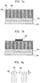
- FIGS. 12a to 12e are sectional views illustrating processes for fabricating a nano rod type light emitting diode according to an embodiment of the method of the present invention.
- a plurality of nano rods (310) formed of a compound semiconductor doped with a first polarity dopant are formed on a base substrate (300) ( FIG. 12a ).
- the base substrate (300) is not a metallic substrate but comprises a substrate made of an oxide-based material such as Al 2 O 3 and Ga 2 O 3 , or a semiconductor material such as Si, SiC and GaAs.
- the nano rods (310) are defined as nano rods and preferably each rod have a width (W) of 1 ⁇ 1,000 nm.
- each of the nano rods (310) be a single-layered nano rod formed of any one selected from Al x Ga 1-x N(0 ⁇ x ⁇ 1), In y Ga 1-y N(0 ⁇ y ⁇ 1), Zn z Mg 1-z O(0 ⁇ z ⁇ 1) and Zn u Cd 1-u O(0 ⁇ u ⁇ 1), or a multi-layered rod formed of a lamination of these materials.
- the nano rods (310) are grown at a temperature range of 200 ⁇ 900 °C using crystal growth equipment such as MOVPE, HVPE and MBE.
- a compound semiconductor doped with a first polarity dopant is grown on the base substrate (300)
- a plurality of nano rods (310) can be formed to be posts each perpendicular to the surface of the base substrate (300).
- the light emitting diode according to the present invention employs a compound semiconductor doped with a first polarity dopant as a material for more specifically implementing the first polarity layer in the light emitting device of the illustrative example.
- an active layer (320) and a compound semiconductor layer (330) doped with a second polarity dopant are sequentially formed on each of the rods (310) to form a light emitting structure (350) including a plurality of nano rod structures (351) spaced apart from one another ( FIG. 12b ).
- the active layer (320) and the compound semiconductor layer (330) doped with a second polarity dopant are formed sequentially on the nano rods (310) to form the nano rod structures (351) spaced apart from one another.
- each of the nano rod structures (351) grows independently from neighboring nano rod structures without interference.
- the active layer (320) comprises a multiple quantum well structure.
- the light emitting structure (350) composed of the plurality of nano rod structures is formed.
- Each of the nano rod structures comprises a compound semiconductor doped with a first polarity dopant, an active layer, and a compound semiconductor doped with a second polarity dopant.
- the first polarity dopant is either an n-type dopant or a p-type dopant
- the second polarity dopant is a dopant having a polarity opposite to that of the first polarity dopant.
- the first polarity dopant and the second polarity dopant have opposite polarities, it is also possible to form nano rods out of a compound semiconductor doped with a second polarity dopant on the base substrate (300).
- the active layer can define a multiple quantum well with a heterojunction by alternately laminating InGaN and GaN.
- an ohmic-contact and reflective electrode (400) is formed on the nano rod structures (351), and a metallic support layer (410) is formed on the ohmic-contact and reflective electrode (400) ( FIG. 12c ).
- the metallic support layer (410) is preferably a layer formed on the ohmic-contact and reflective electrode (400) using any one of an electro-plating process, an electroless plating process, an evaporation process, a sputtering process and a screen printing process.
- the metallic support layer (410) is preferably a prefabricated metallic substrate that is bonded to the ohmic-contact and reflective electrode (400).
- the ohmic contact and reflective electrode 400 may not be formed thereon with the metallic support layer but may be formed with a support layer made of Si, SiC or the like.
- the thickness of the metallic support layer (410) be in a range of 1 ⁇ 100 ⁇ m.
- the base substrate (300) is removed from the nano rod structures (351) ( FIG. 12d ).
- the base substrate (300) is removed using a laser process or a wet etching process.
- an ohmic-contact and transmissive electrode (450) is formed on bottoms of the nano rod structures (351) that have been exposed due to the removal of the base substrate (300) ( FIG. 12e ).
- the ohmic-contact and transmissive electrode (450) refers to, for example, a transparent electrode such as an ITO film.
- the ohmic-contact and reflective electrode (400) is defined as an electrode capable of being in ohmic contact and reflecting light.
- the ohmic-contact and transmissive electrode (450) is defined as an electrode capable of being in ohmic contact and transmitting light.
- the nano rod type light emitting diode of the embodiment of the method of the present invention is completely fabricated.
- the nano rod type light emitting diode comprises the metallic support layer (410); the ohmic-contact and reflective electrode (400) formed on the support layer (410); the plurality of nano rod structures formed on the ohmic-contact and reflective electrode (400) so as to be spaced apart from one another; and the ohmic-contact and transmissive electrode (450) formed on the nano rod structures.
- Each of the nano rod structures comprises the compound semiconductor layer doped with the first polarity dopant, the active layer, and the compound semiconductor doped with the second polarity dopant, which are sequentially formed.
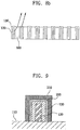
- FIG. 13 is a schematic sectional view illustrating another embodiment of the method for fabricating the nano rod type light emitting diode according to the present invention.
- a buffer layer (307) is formed on a base substrate (300).
- a plurality of nano rods (310) formed of a compound semiconductor doped with a first polarity dopant are formed on the buffer layer (307).
- the plurality of the nano rods (310) are grown at a temperature lower than the growth temperature of the buffer layer (307).
- FIG. 14 is a schematic sectional view illustrating a further embodiment of the method for fabricating the nano rod type light emitting diode according to the present invention.
- a plurality of nano rod structures (351) are formed to be spaced apart from one another.
- Each of the nano rod structures (351) comprises a nano rod (310) made of a compound semiconductor doped with a first polarity dopant, an active layer (320), and a compound semiconductor layer (330) doped with a second polarity dopant, which are sequentially formed.
- a planar compound semiconductor layer (370) doped with a second polarity dopant is , in accordance with the light emitting diode of the present invention, grown on the compound semiconductor layers (330) doped with a second polarity dopant in the plurality of the nano rod structures (351).
- the planar compound semiconductor layer (370) is grown at a temperature higher than the growth temperature of the nano rod structures (351).
- an ohmic-contact and reflective electrode (400) is formed on the planar compound semiconductor layer (370).
- the electrode (400) can be more easily formed on the planar compound semiconductor layer (370) that is doped with a second polarity dopant.
- the nano rod structures (351) are in a state with spaces existing therebetween.
- the flat compound semiconductor layer (370) doped with a second polarity dopant allows for easier formation of the ohmic-contact and reflective electrode (400).
- FIG. 15 is a sectional view illustrating a phenomenon in which light is emitted from the nano rod type light emitting diode fabricated according to the method of the present invention.
- Each of the nano rod structures (351) comprising the nano rod (310) formed of a compound semiconductor doped with a first polarity dopant, the active layer (320), and the compound semiconductor layer (330) doped with a second polarity dopant is a light emitting structure.
- the plurality of nano rod structures emit light in the present invention, there is an advantage in that a light emitting area is increased as compared with a conventional LED where light is emitted from the surface of the diode.
- nano rod structures are spaced apart from one another, there is an advantage in that light scattering can be reduced in the LED and thermal characteristics can be improved.
- a defect called "threading dislocation" occurs with a density of 10 8 ⁇ 10 10 /cm 2 due to lattice mismatch.
- GaN is grown in the form of a thin film and thus a defect remains in the diode.
- stress and strain due to the lattice mismatch can be mitigated and propagation of the threading dislocation into ultra-minute nano rods can be reduced. Therefore, the light emitting structure is grown to have good crystalinity, thereby providing improved characteristics of the LED.
- rods are formed of a material capable of emitting light on a first polarity layer and a second polarity layer is formed to wrap around each of the rods.
- an active layer is formed of a nano rod structure to enhance light extraction efficiency.
- the light emitting structure is grown to have good crystalinity, thereby providing improved characteristics of the light emitting diode.
- nano rod structures are spaced apart from one another, light scattering within the LED of the present invention can be reduced and thermal characteristics can be improved.
Claims (15)
- Diode luminescente, LED (« light emitting diode »), de type à nanotiges, comprenant :une couche de support métallique (410) ;une électrode réfléchissante et de contact ohmique (400) sur la couche de support métallique (410) ;une pluralité de structures de nanotiges (351) sur l'électrode réfléchissante et de contact ohmique, chaque structure de nanotige (351) comprenant séquentiellement : une couche de semi-conducteur composé de première polarité (310), une couche active (320) et une couche de semi-conducteur composé de seconde polarité (330) dont la polarité est opposée à celle de la couche de semi-conducteur composé de première polarité (310), et séparées les unes des autres ;une électrode transmissive et de contact ohmique (450) sur la pluralité de structures de nanotiges (351) ; etune couche de semi-conducteur composé plane (370) entre la pluralité de structures de nanotiges (351) et l'électrode réfléchissante et de contact ohmique (400), dont la polarité est la seconde.
- LED selon la revendication 1, comprenant en outre une couche tampon (307) entre la pluralité de structures de nanotiges (351) et l'électrode transmissive et de contact ohmique (450).
- LED selon la revendication 1 ou 2, dans laquelle la couche de support métallique (410) a une épaisseur dans une plage de 1 à 100 µm.
- LED selon la revendication 1 ou 2, dans laquelle l'électrode transmissive et de contact ohmique (450) inclut un film d'ITO.
- LED selon la revendication 1 ou 2, dans laquelle les nanotiges (310) sont des nanotiges monocouches formées d'un composé quelconque choisi parmi AlxGa1-xN (0 ≤ x ≤ 1), InyGa1-yN (0 ≤ y ≤ 1), ZnzMg1-zO (0 ≤ z ≤ 1) et ZnuCd1-uO (0 ≤ u ≤ 1).
- LED selon la revendication 1 ou 2, dans laquelle les nanotiges (310) sont des nanotiges multicouches formées d'un composé quelconque choisi parmi AlxGa1-xN(0 ≤ x ≤ 1), InyGa1-yN (0 ≤ y ≤ 1), ZnzMg1-zO (0 ≤ z ≤ 1) ou ZnuCd1-uO (0 ≤ u ≤ 1).
- LED selon l'une quelconque des revendications 1 à 4, dans laquelle les structures de nanotiges (351) ont une largeur dans une plage de 1 à 1000 nm.
- Procédé de fabrication d'une diode luminescente, LED (« light emitting diode »), de type à nanotiges, le procédé comprenant :faire croître une pluralité de nanotiges sur un substrat (300), les nanotiges incluant une couche de semi-conducteur composé de première polarité (310) ;former une pluralité de structures de nanotiges (351) en faisant croître une couche active (320) et une couche de semi-conducteur composé de seconde polarité (330), dont la polarité est opposée à celle de la couche de semi-conducteur composé de première polarité (310), sur les nanotiges ;former une électrode réfléchissante et de contact ohmique (400) sur la pluralité de structures de nanotiges (351) ;former une couche de support métallique (410) sur l'électrode réfléchissante et de contact ohmique (400) ;éliminer le substrat (300) ; etformer une électrode transmissive et de contact ohmique (450) sur la pluralité de structures de nanotiges (351).
- Procédé selon la revendication 8, comprenant en outre :
faire croître une couche de semi-conducteur composé plane (370) sur la pluralité de structures de nanotiges (351), dont la polarité est la seconde. - Procédé selon la revendication 8, comprenant en outre: faire croître une couche tampon (307) sur le substrat (300).
- Procédé selon l'une quelconque des revendications 8 à 10, dans lequel faire croître la pluralité de nanotiges comprend :faire croître un semi-conducteur composé sur le substrat (300) pour former une pluralité de germes (305) sur le substrat ; etfaire croître la pluralité de germes pour former la pluralité de nanotiges.
- Procédé selon l'une quelconque des revendications 8 à 11, dans lequel l'électrode transmissive et de contact ohmique (450) inclut un film d'ITO.
- Procédé selon l'une quelconque des revendications 8 à 12, dans lequel les nanotiges sont des nanotiges monocouches formées d'un composé quelconque choisi parmi AlxGa1-xN (0 ≤ x ≤ 1), InyGa1-yN (0 ≤ y ≤ 1), ZnzMg1-zO (0 ≤ z ≤ 1) et ZnuCd1-uO (0 ≤ u ≤ 1).
- Procédé selon l'une quelconque des revendications 8 à 13, dans lequel les nanotiges sont des nanotiges multicouches formées d'un composé quelconque choisi parmi AlxGa1-xN (0 ≤ x ≤ 1), InyGa1-yN (0 ≤ y ≤ 1), ZnzMg1-zO (0 ≤ z ≤ 1) et ZnuCd1-uO (0 ≤ u ≤ 1).
- Procédé selon l'une quelconque des revendications 8 à 14, dans lequel les structures de nanotiges (351) ont une largeur dans une plage de 1 à 1000 nm.
Applications Claiming Priority (3)
| Application Number | Priority Date | Filing Date | Title |
|---|---|---|---|
| KR1020050043577A KR100658938B1 (ko) | 2005-05-24 | 2005-05-24 | 나노 로드를 갖는 발광 소자 및 그의 제조 방법 |
| KR1020050044373A KR101129094B1 (ko) | 2005-05-26 | 2005-05-26 | 로드형 발광 소자 및 그의 제조방법 |
| EP06290812.4A EP1727216B1 (fr) | 2005-05-24 | 2006-05-18 | Diode électroluminescente à bâtonnets et procédé de fabrication correspondant |
Related Parent Applications (3)
| Application Number | Title | Priority Date | Filing Date |
|---|---|---|---|
| EP06290812.4 Division | 2006-05-18 | ||
| EP06290812.4A Division-Into EP1727216B1 (fr) | 2005-05-24 | 2006-05-18 | Diode électroluminescente à bâtonnets et procédé de fabrication correspondant |
| EP06290812.4A Division EP1727216B1 (fr) | 2005-05-24 | 2006-05-18 | Diode électroluminescente à bâtonnets et procédé de fabrication correspondant |
Publications (3)
| Publication Number | Publication Date |
|---|---|
| EP2410582A2 EP2410582A2 (fr) | 2012-01-25 |
| EP2410582A3 EP2410582A3 (fr) | 2013-10-23 |
| EP2410582B1 true EP2410582B1 (fr) | 2019-09-04 |
Family
ID=36791575
Family Applications (2)
| Application Number | Title | Priority Date | Filing Date |
|---|---|---|---|
| EP11186011.0A Active EP2410582B1 (fr) | 2005-05-24 | 2006-05-18 | Diode électroluminescente à nano-bâtonnets et procédé de fabrication d'une diode électroluminescente à nano-bâtonnets |
| EP06290812.4A Active EP1727216B1 (fr) | 2005-05-24 | 2006-05-18 | Diode électroluminescente à bâtonnets et procédé de fabrication correspondant |
Family Applications After (1)
| Application Number | Title | Priority Date | Filing Date |
|---|---|---|---|
| EP06290812.4A Active EP1727216B1 (fr) | 2005-05-24 | 2006-05-18 | Diode électroluminescente à bâtonnets et procédé de fabrication correspondant |
Country Status (3)
| Country | Link |
|---|---|
| US (2) | US7947989B2 (fr) |
| EP (2) | EP2410582B1 (fr) |
| JP (1) | JP4740795B2 (fr) |
Families Citing this family (83)
| Publication number | Priority date | Publication date | Assignee | Title |
|---|---|---|---|---|
| EP1821347B1 (fr) * | 2006-02-16 | 2018-01-03 | LG Electronics Inc. | Dispositif luminescent de structure verticale et son procédé de fabrication |
| FR2902237B1 (fr) * | 2006-06-09 | 2008-10-10 | Commissariat Energie Atomique | Procede de realisation d'un dispositif microelectronique emetteur de lumiere a nanofils semi-conducteurs formes sur un substrat metallique |
| JP2008066590A (ja) * | 2006-09-08 | 2008-03-21 | Matsushita Electric Works Ltd | 化合物半導体発光素子およびそれを用いる照明装置ならびに化合物半導体素子の製造方法 |
| JP2008098220A (ja) * | 2006-10-06 | 2008-04-24 | Asahi Kasei Corp | 発光ダイオード |
| WO2008079076A1 (fr) | 2006-12-22 | 2008-07-03 | Qunano Ab | Diode électroluminescente avec structure de nanofil verticale et procédé de fabrication de celle-ci |
| EP2091862B1 (fr) * | 2006-12-22 | 2019-12-11 | QuNano AB | Diode électroluminescente surélevée et son procédé de production |
| WO2008079077A2 (fr) * | 2006-12-22 | 2008-07-03 | Qunano Ab | Structure nanoélectronique et procédé de production associé |
| US8049203B2 (en) | 2006-12-22 | 2011-11-01 | Qunano Ab | Nanoelectronic structure and method of producing such |
| WO2008082097A1 (fr) | 2006-12-28 | 2008-07-10 | Seoul Opto Device Co., Ltd. | Dispositif émettant de la lumière et procédé de fabrication de celui-ci |
| US7829443B2 (en) | 2007-01-12 | 2010-11-09 | Qunano Ab | Nitride nanowires and method of producing such |
| WO2008129859A1 (fr) * | 2007-04-13 | 2008-10-30 | Panasonic Corporation | Elément d'émission de lumière et dispositif d'affichage |
| JP5112761B2 (ja) * | 2007-06-26 | 2013-01-09 | パナソニック株式会社 | 化合物半導体素子およびそれを用いる照明装置ならびに化合物半導体素子の製造方法 |
| KR20090012493A (ko) * | 2007-07-30 | 2009-02-04 | 삼성전기주식회사 | 광자결정 발광소자 |
| JP5247109B2 (ja) * | 2007-10-05 | 2013-07-24 | パナソニック株式会社 | 半導体発光装置およびそれを用いる照明装置ならびに半導体発光装置の製造方法 |
| FR2922685B1 (fr) * | 2007-10-22 | 2011-02-25 | Commissariat Energie Atomique | Dispositif optoelectronique a base de nanofils et procedes correspondants |
| US8084337B2 (en) * | 2007-10-26 | 2011-12-27 | Qunano Ab | Growth of III-V compound semiconductor nanowires on silicon substrates |
| KR20090058952A (ko) * | 2007-12-05 | 2009-06-10 | 삼성전자주식회사 | 나노로드를 이용한 발광소자 및 그 제조 방법 |
| JP5097532B2 (ja) * | 2007-12-21 | 2012-12-12 | パナソニック株式会社 | 化合物半導体発光素子の製造方法 |
| JP4856666B2 (ja) * | 2008-03-26 | 2012-01-18 | 独立行政法人科学技術振興機構 | 発光ダイオード素子及びその製造方法 |
| KR101496151B1 (ko) * | 2008-06-25 | 2015-02-27 | 삼성전자주식회사 | 산화물 다이오드를 이용한 디스플레이 장치 |
| WO2010014032A1 (fr) | 2008-07-07 | 2010-02-04 | Glo Ab | Del nanostructurée |
| US20110168976A1 (en) * | 2008-07-24 | 2011-07-14 | The Regents Of The University Of California | Micro- and nano-structured led and oled devices |
| KR100956499B1 (ko) * | 2008-08-01 | 2010-05-07 | 주식회사 실트론 | 금속층을 가지는 화합물 반도체 기판, 그 제조 방법 및이를 이용한 화합물 반도체 소자 |
| WO2010022064A1 (fr) * | 2008-08-21 | 2010-02-25 | Nanocrystal Corporation | Nanostructures de nitrure du groupe iii sans défaut et dispositifs utilisant des techniques de croissance pulsée et non pulsée |
| TWI379443B (en) * | 2008-11-28 | 2012-12-11 | Univ Nat Taiwan | A lighting device having high efficiency and a method for fabricating the same |
| KR101061150B1 (ko) | 2009-05-22 | 2011-08-31 | 서울대학교산학협력단 | 발광 디바이스와 이의 제조 방법 |
| US8872214B2 (en) | 2009-10-19 | 2014-10-28 | Sharp Kabushiki Kaisha | Rod-like light-emitting device, method of manufacturing rod-like light-emitting device, backlight, illuminating device, and display device |
| JP5094824B2 (ja) * | 2009-10-19 | 2012-12-12 | シャープ株式会社 | 棒状構造発光素子、バックライト、照明装置および表示装置 |
| JP5014403B2 (ja) * | 2009-11-19 | 2012-08-29 | シャープ株式会社 | 棒状構造発光素子、発光装置、発光装置の製造方法、バックライト、照明装置および表示装置 |
| JP2011119617A (ja) * | 2009-12-07 | 2011-06-16 | Sharp Corp | 棒状構造発光素子の製造方法 |
| JP5066164B2 (ja) * | 2009-12-07 | 2012-11-07 | シャープ株式会社 | 半導体素子の製造方法 |
| US9329433B2 (en) | 2010-03-12 | 2016-05-03 | Sharp Kabushiki Kaisha | Light-emitting device manufacturing method, light-emitting device, lighting device, backlight, liquid-crystal panel, display device, display device manufacturing method, display device drive method and liquid-crystal display device |
| JP2011198697A (ja) * | 2010-03-23 | 2011-10-06 | Sharp Corp | 発光装置、発光装置の製造方法、照明装置およびバックライト |
| DE102010012711A1 (de) * | 2010-03-25 | 2011-09-29 | Osram Opto Semiconductors Gmbh | Strahlungsemittierendes Halbleiterbauelement und Verfahren zur Herstellung eines strahlungsemittierenden Halbleiterbauelements |
| US8669125B2 (en) | 2010-06-18 | 2014-03-11 | Glo Ab | Nanowire LED structure and method for manufacturing the same |
| KR20130093115A (ko) | 2010-09-01 | 2013-08-21 | 샤프 가부시키가이샤 | 발광 소자 및 그 제조 방법, 발광 장치의 제조 방법, 조명 장치, 백라이트, 표시 장치 및 다이오드 |
| JP4927223B2 (ja) * | 2010-09-01 | 2012-05-09 | シャープ株式会社 | 発光素子およびその製造方法、発光装置の製造方法、照明装置、バックライト並びに表示装置 |
| FR2975532B1 (fr) * | 2011-05-18 | 2013-05-10 | Commissariat Energie Atomique | Connexion electrique en serie de nanofils emetteurs de lumiere |
| KR101217209B1 (ko) * | 2010-10-07 | 2012-12-31 | 서울대학교산학협력단 | 발광소자 및 그 제조방법 |
| TWI573288B (zh) * | 2010-10-18 | 2017-03-01 | 鴻海精密工業股份有限公司 | 發光二極體及其製作方法 |
| CN102456786B (zh) * | 2010-10-29 | 2016-03-09 | 鸿富锦精密工业(深圳)有限公司 | 发光二极管及其制作方法 |
| DE102010051286A1 (de) * | 2010-11-12 | 2012-05-16 | Osram Opto Semiconductors Gmbh | Optoelektronischer Halbleiterchip und Verfahren zu dessen Herstellung |
| TWI419367B (zh) * | 2010-12-02 | 2013-12-11 | Epistar Corp | 光電元件及其製造方法 |
| TWI495155B (zh) * | 2010-12-02 | 2015-08-01 | Epistar Corp | 光電元件及其製造方法 |
| GB201021112D0 (en) | 2010-12-13 | 2011-01-26 | Ntnu Technology Transfer As | Nanowires |
| US20120146069A1 (en) * | 2010-12-14 | 2012-06-14 | International Business Machines Corporation | Oxide Based LED BEOL Integration |
| KR101209449B1 (ko) * | 2011-04-29 | 2012-12-07 | 피에스아이 주식회사 | 풀-칼라 led 디스플레이 장치 및 그 제조방법 |
| CN102185068A (zh) * | 2011-05-06 | 2011-09-14 | 西安神光安瑞光电科技有限公司 | 发光二极管及其制备方法 |
| CN102185070A (zh) * | 2011-05-06 | 2011-09-14 | 西安神光安瑞光电科技有限公司 | 发光二极管及其制备方法 |
| US8604491B2 (en) | 2011-07-21 | 2013-12-10 | Tsmc Solid State Lighting Ltd. | Wafer level photonic device die structure and method of making the same |
| DE102011112706B4 (de) | 2011-09-07 | 2021-09-02 | OSRAM Opto Semiconductors Gesellschaft mit beschränkter Haftung | Optoelektronisches Bauelement |
| US8350249B1 (en) * | 2011-09-26 | 2013-01-08 | Glo Ab | Coalesced nanowire structures with interstitial voids and method for manufacturing the same |
| DE102011056140A1 (de) * | 2011-12-07 | 2013-06-13 | Osram Opto Semiconductors Gmbh | Optoelektronischer Halbleiterchip |
| FR2984599B1 (fr) | 2011-12-20 | 2014-01-17 | Commissariat Energie Atomique | Procede de fabrication d'un micro- ou nano- fil semiconducteur, structure semiconductrice comportant un tel micro- ou nano- fil et procede de fabrication d'une structure semiconductrice |
| EP2815423B1 (fr) | 2012-02-14 | 2017-05-24 | Hexagem AB | Electronique à base de nanofil de nitrure de gallium |
| DE102012101718A1 (de) * | 2012-03-01 | 2013-09-05 | Osram Opto Semiconductors Gmbh | Optoelektronischer Halbleiterchip |
| GB201211038D0 (en) | 2012-06-21 | 2012-08-01 | Norwegian Univ Sci & Tech Ntnu | Solar cells |
| KR101898679B1 (ko) | 2012-12-14 | 2018-10-04 | 삼성전자주식회사 | 나노구조 발광소자 |
| FR3000294B1 (fr) * | 2012-12-21 | 2016-03-04 | Aledia | Support fonctionnel comprenant des nanofils et des nano-empreintes et procede de fabrication dudit support |
| KR101603207B1 (ko) | 2013-01-29 | 2016-03-14 | 삼성전자주식회사 | 나노구조 반도체 발광소자 제조방법 |
| WO2014138904A1 (fr) * | 2013-03-14 | 2014-09-18 | The Royal Institution For The Advancement Of Learning/Mcgill University | Procédés et dispositifs pour dispositifs à nanofils à semi-conducteur |
| FR3004000B1 (fr) * | 2013-03-28 | 2016-07-15 | Aledia | Dispositif electroluminescent avec capteur integre et procede de controle de l'emission du dispositif |
| FR3004006B1 (fr) * | 2013-03-28 | 2016-10-07 | Aledia | Dispositif electroluminescent a nanofils actifs et nanofils de contact et procede de fabrication |
| GB201311101D0 (en) | 2013-06-21 | 2013-08-07 | Norwegian Univ Sci & Tech Ntnu | Semiconducting Films |
| FR3011383B1 (fr) * | 2013-09-30 | 2017-05-26 | Commissariat Energie Atomique | Procede de fabrication de dispositifs optoelectroniques a diodes electroluminescentes |
| US9099573B2 (en) | 2013-10-31 | 2015-08-04 | Samsung Electronics Co., Ltd. | Nano-structure semiconductor light emitting device |
| KR102285786B1 (ko) * | 2014-01-20 | 2021-08-04 | 삼성전자 주식회사 | 반도체 발광 소자 |
| WO2016022824A1 (fr) | 2014-08-08 | 2016-02-11 | Glo Ab | Dispositif d'affichage pixélisé basé sur des led à nanofils et son procédé de fabrication |
| KR102227771B1 (ko) | 2014-08-25 | 2021-03-16 | 삼성전자주식회사 | 나노구조 반도체 발광소자 |
| WO2016049507A1 (fr) | 2014-09-26 | 2016-03-31 | Glo Ab | Puce d'image monolithique pour affichage proche de l'œil |
| US10347791B2 (en) | 2015-07-13 | 2019-07-09 | Crayonano As | Nanowires or nanopyramids grown on graphitic substrate |
| AU2016292849B2 (en) | 2015-07-13 | 2019-05-16 | Crayonano As | Nanowires/nanopyramids shaped light emitting diodes and photodetectors |
| KR20180053652A (ko) | 2015-07-31 | 2018-05-23 | 크래요나노 에이에스 | 그라파이트 기판 상에 나노와이어 또는 나노피라미드를 성장시키는 방법 |
| US10374127B2 (en) * | 2015-09-17 | 2019-08-06 | Nxp Usa, Inc. | Electronic devices with nanorings, and methods of manufacture thereof |
| JP6149247B1 (ja) * | 2016-11-21 | 2017-06-21 | 株式会社奥本研究所 | 発光デバイスおよびその製造方法 |
| KR20180071465A (ko) | 2016-12-19 | 2018-06-28 | 삼성디스플레이 주식회사 | 발광장치 및 그의 제조방법 |
| KR102587958B1 (ko) * | 2017-02-03 | 2023-10-11 | 삼성전자주식회사 | 메타 광학 소자 및 그 제조 방법 |
| FR3063129B1 (fr) * | 2017-02-17 | 2019-04-12 | Valeo Vision | Module lumineux a encombrement reduit |
| GB201705755D0 (en) * | 2017-04-10 | 2017-05-24 | Norwegian Univ Of Science And Tech (Ntnu) | Nanostructure |
| US11063178B2 (en) * | 2017-10-25 | 2021-07-13 | Sensor Electronic Technology, Inc. | Semiconductor heterostructure with improved light emission |
| CN108565322A (zh) * | 2018-06-01 | 2018-09-21 | 广东工业大学 | 一种led外延芯片及一种led外延芯片的制备方法 |
| FR3083002B1 (fr) * | 2018-06-20 | 2020-07-31 | Aledia | Dispositif optoelectronique comprenant une matrice de diodes |
| GB2575311B (en) * | 2018-07-06 | 2021-03-03 | Plessey Semiconductors Ltd | Monolithic LED array and a precursor thereto |
Family Cites Families (46)
| Publication number | Priority date | Publication date | Assignee | Title |
|---|---|---|---|---|
| US4920793A (en) * | 1986-05-23 | 1990-05-01 | Djorup Robert Sonny | Directional thermal anemometer transducer |
| JPH06244457A (ja) * | 1993-02-16 | 1994-09-02 | Nisshin Steel Co Ltd | 発光ダイオードの製造方法 |
| CN1082254C (zh) * | 1995-08-22 | 2002-04-03 | 松下电器产业株式会社 | 硅结构体及其制造方法和装置及使用硅结构体的太阳电池 |
| JP3517091B2 (ja) * | 1997-07-04 | 2004-04-05 | 東芝電子エンジニアリング株式会社 | 窒化ガリウム系半導体発光素子およびその製造方法 |
| JP4083866B2 (ja) * | 1998-04-28 | 2008-04-30 | シャープ株式会社 | 半導体レーザ素子 |
| JP2000208874A (ja) * | 1999-01-12 | 2000-07-28 | Sony Corp | 窒化物半導体と、窒化物半導体発光装置と、窒化物半導体の製造方法と、半導体発光装置の製造方法 |
| US6992334B1 (en) * | 1999-12-22 | 2006-01-31 | Lumileds Lighting U.S., Llc | Multi-layer highly reflective ohmic contacts for semiconductor devices |
| JP3662806B2 (ja) * | 2000-03-29 | 2005-06-22 | 日本電気株式会社 | 窒化物系半導体層の製造方法 |
| JP3882539B2 (ja) * | 2000-07-18 | 2007-02-21 | ソニー株式会社 | 半導体発光素子およびその製造方法、並びに画像表示装置 |
| US20020017652A1 (en) * | 2000-08-08 | 2002-02-14 | Stefan Illek | Semiconductor chip for optoelectronics |
| JP4672839B2 (ja) * | 2000-09-06 | 2011-04-20 | キヤノン株式会社 | 発光体、構造体及びその製造方法 |
| JP4595198B2 (ja) * | 2000-12-15 | 2010-12-08 | ソニー株式会社 | 半導体発光素子及び半導体発光素子の製造方法 |
| JP3946969B2 (ja) * | 2001-05-31 | 2007-07-18 | 日本碍子株式会社 | 電界効果トランジスタ、及びヘテロ接合型バイポーラトランジスタ |
| WO2003015143A1 (fr) * | 2001-08-01 | 2003-02-20 | Nagoya Industrial Science Research Institute | Film semi-conducteur en nitrure du groupe iii et son procede de production |
| JP4254157B2 (ja) * | 2001-08-22 | 2009-04-15 | ソニー株式会社 | 窒化物半導体素子及び窒化物半導体素子の製造方法 |
| KR20040029301A (ko) * | 2001-08-22 | 2004-04-06 | 소니 가부시끼 가이샤 | 질화물 반도체소자 및 질화물 반도체소자의 제조방법 |
| JP2003101069A (ja) * | 2001-09-25 | 2003-04-04 | Nagoya Industrial Science Research Inst | Iii族窒化物量子ドットおよびその製造方法 |
| JP3988429B2 (ja) * | 2001-10-10 | 2007-10-10 | ソニー株式会社 | 半導体発光素子、画像表示装置及び照明装置とその製造方法 |
| TWI220319B (en) * | 2002-03-11 | 2004-08-11 | Solidlite Corp | Nano-wire light emitting device |
| JP4514402B2 (ja) * | 2002-10-28 | 2010-07-28 | シャープ株式会社 | 半導体素子及びその製造方法 |
| AU2003274418A1 (en) * | 2002-11-05 | 2004-06-07 | Koninklijke Philips Electronics N.V. | Nanostructure, electronic device having such nanostructure and method of preparing nanostructure |
| US6969897B2 (en) * | 2002-12-10 | 2005-11-29 | Kim Ii John | Optoelectronic devices employing fibers for light collection and emission |
| JP2004288799A (ja) * | 2003-03-20 | 2004-10-14 | Sony Corp | 半導体発光素子およびその製造方法、集積型半導体発光装置およびその製造方法、画像表示装置およびその製造方法ならびに照明装置およびその製造方法 |
| US20040252737A1 (en) * | 2003-06-16 | 2004-12-16 | Gyu Chul Yi | Zinc oxide based nanorod with quantum well or coaxial quantum structure |
| KR100593264B1 (ko) * | 2003-06-26 | 2006-06-26 | 학교법인 포항공과대학교 | p-타입 반도체 박막과 n-타입 산화아연(ZnO)계나노막대의 이종접합 구조체, 이의 제법 및 이를 이용한소자 |
| US20050040212A1 (en) * | 2003-08-23 | 2005-02-24 | Kuang-Neng Yang | Method for manufacturing nitride light-emitting device |
| KR100644166B1 (ko) * | 2004-02-12 | 2006-11-10 | 학교법인 포항공과대학교 | 질화물 반도체의 이종접합 구조체, 이를 포함하는나노소자 또는 이의 어레이 |
| JP4160000B2 (ja) * | 2004-02-13 | 2008-10-01 | ドンゴク ユニバーシティ インダストリー アカデミック コーポレイション ファウンデイション | 発光ダイオードおよびその製造方法 |
| KR100646696B1 (ko) * | 2004-03-10 | 2006-11-23 | 주식회사 실트론 | 질화물 반도체 소자 및 그 제조방법 |
| KR100624419B1 (ko) * | 2004-04-07 | 2006-09-19 | 삼성전자주식회사 | 나노와이어 발광소자 및 그 제조방법 |
| KR100553317B1 (ko) * | 2004-04-23 | 2006-02-20 | 한국과학기술연구원 | 실리콘 나노선을 이용한 실리콘 광소자 및 이의 제조방법 |
| KR100616600B1 (ko) * | 2004-08-24 | 2006-08-28 | 삼성전기주식회사 | 수직구조 질화물 반도체 발광소자 |
| KR100664986B1 (ko) * | 2004-10-29 | 2007-01-09 | 삼성전기주식회사 | 나노로드를 이용한 질화물계 반도체 소자 및 그 제조 방법 |
| US7180097B2 (en) * | 2004-11-12 | 2007-02-20 | Formosa Epitaxy Incorporation | High-brightness gallium-nitride based light emitting diode structure |
| US7202173B2 (en) * | 2004-12-20 | 2007-04-10 | Palo Alto Research Corporation Incorporated | Systems and methods for electrical contacts to arrays of vertically aligned nanorods |
| US20060207647A1 (en) * | 2005-03-16 | 2006-09-21 | General Electric Company | High efficiency inorganic nanorod-enhanced photovoltaic devices |
| CN1850580A (zh) * | 2005-04-22 | 2006-10-25 | 清华大学 | 超晶格纳米器件及其制作方法 |
| US8330173B2 (en) * | 2005-06-25 | 2012-12-11 | Seoul Opto Device Co., Ltd. | Nanostructure having a nitride-based quantum well and light emitting diode employing the same |
| KR20070021671A (ko) * | 2005-08-19 | 2007-02-23 | 서울옵토디바이스주식회사 | 나노막대들의 어레이를 채택한 발광 다이오드 및 그것을제조하는 방법 |
| US7635600B2 (en) * | 2005-11-16 | 2009-12-22 | Sharp Laboratories Of America, Inc. | Photovoltaic structure with a conductive nanowire array electrode |
| AU2007313096B2 (en) * | 2006-03-10 | 2011-11-10 | Unm Rainforest Innovations | Pulsed growth of GaN nanowires and applications in group III nitride semiconductor substrate materials and devices |
| EP2091862B1 (fr) * | 2006-12-22 | 2019-12-11 | QuNano AB | Diode électroluminescente surélevée et son procédé de production |
| TWI411124B (zh) * | 2007-07-10 | 2013-10-01 | Delta Electronics Inc | 發光二極體裝置及其製造方法 |
| KR20090058952A (ko) * | 2007-12-05 | 2009-06-10 | 삼성전자주식회사 | 나노로드를 이용한 발광소자 및 그 제조 방법 |
| TWI389346B (zh) * | 2008-10-01 | 2013-03-11 | Epistar Corp | 光電元件 |
| TWI396307B (zh) * | 2009-02-05 | 2013-05-11 | Huga Optotech Inc | 發光二極體 |
-
2006
- 2006-05-18 EP EP11186011.0A patent/EP2410582B1/fr active Active
- 2006-05-18 JP JP2006139266A patent/JP4740795B2/ja active Active
- 2006-05-18 EP EP06290812.4A patent/EP1727216B1/fr active Active
- 2006-05-19 US US11/436,771 patent/US7947989B2/en active Active
-
2011
- 2011-04-15 US US13/088,139 patent/US8653538B2/en active Active
Non-Patent Citations (1)
| Title |
|---|
| None * |
Also Published As
| Publication number | Publication date |
|---|---|
| US20110272723A1 (en) | 2011-11-10 |
| EP2410582A3 (fr) | 2013-10-23 |
| EP1727216B1 (fr) | 2019-04-24 |
| US8653538B2 (en) | 2014-02-18 |
| EP2410582A2 (fr) | 2012-01-25 |
| JP4740795B2 (ja) | 2011-08-03 |
| JP2006332650A (ja) | 2006-12-07 |
| US20070041214A1 (en) | 2007-02-22 |
| EP1727216A2 (fr) | 2006-11-29 |
| US7947989B2 (en) | 2011-05-24 |
| EP1727216A3 (fr) | 2011-07-27 |
Similar Documents
| Publication | Publication Date | Title |
|---|---|---|
| EP2410582B1 (fr) | Diode électroluminescente à nano-bâtonnets et procédé de fabrication d'une diode électroluminescente à nano-bâtonnets | |
| JP4927042B2 (ja) | 光子結晶発光素子及びその製造方法 | |
| US7893448B2 (en) | Light emitting device having nano structures for light extraction | |
| US7816700B2 (en) | Light emitting diode employing an array of nanorods and method of fabricating the same | |
| US8847199B2 (en) | Nanorod light emitting device and method of manufacturing the same | |
| US7763881B2 (en) | Photonic crystal light emitting device | |
| US20040094772A1 (en) | Gallium nitride based compound semiconductor light-emitting device and manufacturing method therefor | |
| JP4339822B2 (ja) | 発光装置 | |
| JP2005277423A (ja) | 高効率発光素子 | |
| JP5038382B2 (ja) | 半導体発光素子 | |
| KR20120055391A (ko) | 나노로드 발광소자 | |
| JP5989318B2 (ja) | 半導体発光素子及びその製造方法 | |
| JP5165668B2 (ja) | 半導体発光素子及びその製造方法 | |
| JP4751093B2 (ja) | 半導体発光素子 | |
| KR20110091245A (ko) | 반도체 발광소자 및 그 제조방법 | |
| KR102453545B1 (ko) | 나노막대를 포함하는 나노막대 발광 구조물, 발광소자 및 그 제조방법, 그의 패키지 및 이를 포함하는 조명장치 | |
| KR20200111323A (ko) | 반도체 발광소자 및 그 제조 방법 | |
| KR20110091246A (ko) | 반도체 발광소자의 제조방법 및 이에 의해 제조된 반도체 발광소자 | |
| KR101762176B1 (ko) | 나노로드 발광소자 | |
| KR101428068B1 (ko) | 그룹 3족 질화물계 반도체 발광다이오드 소자 및 이의 제조방법 | |
| KR20110094976A (ko) | 발광 소자 및 그 제조 방법 |
Legal Events
| Date | Code | Title | Description |
|---|---|---|---|
| AC | Divisional application: reference to earlier application |
Ref document number: 1727216 Country of ref document: EP Kind code of ref document: P |
|
| AK | Designated contracting states |
Kind code of ref document: A2 Designated state(s): AT BE BG CH CY CZ DE DK EE ES FI FR GB GR HU IE IS IT LI LT LU LV MC NL PL PT RO SE SI SK TR |
|
| PUAI | Public reference made under article 153(3) epc to a published international application that has entered the european phase |
Free format text: ORIGINAL CODE: 0009012 |
|
| PUAL | Search report despatched |
Free format text: ORIGINAL CODE: 0009013 |
|
| AK | Designated contracting states |
Kind code of ref document: A3 Designated state(s): AT BE BG CH CY CZ DE DK EE ES FI FR GB GR HU IE IS IT LI LT LU LV MC NL PL PT RO SE SI SK TR |
|
| RIC1 | Information provided on ipc code assigned before grant |
Ipc: H01L 33/00 20100101AFI20130918BHEP Ipc: H01L 33/32 20100101ALN20130918BHEP Ipc: B82Y 20/00 20110101ALN20130918BHEP Ipc: H01L 33/08 20100101ALN20130918BHEP Ipc: H01L 33/18 20100101ALI20130918BHEP Ipc: H01L 33/28 20100101ALN20130918BHEP |
|
| 17P | Request for examination filed |
Effective date: 20140331 |
|
| RBV | Designated contracting states (corrected) |
Designated state(s): AT BE BG CH CY CZ DE DK EE ES FI FR GB GR HU IE IS IT LI LT LU LV MC NL PL PT RO SE SI SK TR |
|
| RAP1 | Party data changed (applicant data changed or rights of an application transferred) |
Owner name: LG INNOTEK CO., LTD. Owner name: LG ELECTRONICS INC. |
|
| RAP1 | Party data changed (applicant data changed or rights of an application transferred) |
Owner name: LG INNOTEK CO., LTD. Owner name: LG ELECTRONICS INC. |
|
| REG | Reference to a national code |
Ref country code: DE Ref legal event code: R079 Ref document number: 602006058561 Country of ref document: DE Free format text: PREVIOUS MAIN CLASS: H01L0033080000 Ipc: H01L0033180000 |
|
| GRAP | Despatch of communication of intention to grant a patent |
Free format text: ORIGINAL CODE: EPIDOSNIGR1 |
|
| STAA | Information on the status of an ep patent application or granted ep patent |
Free format text: STATUS: GRANT OF PATENT IS INTENDED |
|
| RIC1 | Information provided on ipc code assigned before grant |
Ipc: H01L 33/28 20100101ALN20190220BHEP Ipc: H01L 33/18 20100101AFI20190220BHEP Ipc: H01L 33/42 20100101ALN20190220BHEP Ipc: H01L 33/08 20100101ALN20190220BHEP Ipc: H01L 33/32 20100101ALN20190220BHEP Ipc: B82Y 20/00 20110101ALN20190220BHEP Ipc: H01L 33/00 20100101ALI20190220BHEP Ipc: H01L 33/40 20100101ALN20190220BHEP |
|
| INTG | Intention to grant announced |
Effective date: 20190319 |
|
| GRAS | Grant fee paid |
Free format text: ORIGINAL CODE: EPIDOSNIGR3 |
|
| GRAA | (expected) grant |
Free format text: ORIGINAL CODE: 0009210 |
|
| STAA | Information on the status of an ep patent application or granted ep patent |
Free format text: STATUS: THE PATENT HAS BEEN GRANTED |
|
| RAP1 | Party data changed (applicant data changed or rights of an application transferred) |
Owner name: LG ELECTRONICS INC. Owner name: LG INNOTEK CO., LTD. |
|
| AC | Divisional application: reference to earlier application |
Ref document number: 1727216 Country of ref document: EP Kind code of ref document: P |
|
| AK | Designated contracting states |
Kind code of ref document: B1 Designated state(s): AT BE BG CH CY CZ DE DK EE ES FI FR GB GR HU IE IS IT LI LT LU LV MC NL PL PT RO SE SI SK TR |
|
| REG | Reference to a national code |
Ref country code: GB Ref legal event code: FG4D |
|
| REG | Reference to a national code |
Ref country code: CH Ref legal event code: EP |
|
| REG | Reference to a national code |
Ref country code: AT Ref legal event code: REF Ref document number: 1176598 Country of ref document: AT Kind code of ref document: T Effective date: 20190915 |
|
| REG | Reference to a national code |
Ref country code: DE Ref legal event code: R096 Ref document number: 602006058561 Country of ref document: DE |
|
| REG | Reference to a national code |
Ref country code: IE Ref legal event code: FG4D |
|
| REG | Reference to a national code |
Ref country code: NL Ref legal event code: MP Effective date: 20190904 |
|
| REG | Reference to a national code |
Ref country code: LT Ref legal event code: MG4D |
|
| PG25 | Lapsed in a contracting state [announced via postgrant information from national office to epo] |
Ref country code: SE Free format text: LAPSE BECAUSE OF FAILURE TO SUBMIT A TRANSLATION OF THE DESCRIPTION OR TO PAY THE FEE WITHIN THE PRESCRIBED TIME-LIMIT Effective date: 20190904 Ref country code: LT Free format text: LAPSE BECAUSE OF FAILURE TO SUBMIT A TRANSLATION OF THE DESCRIPTION OR TO PAY THE FEE WITHIN THE PRESCRIBED TIME-LIMIT Effective date: 20190904 Ref country code: BG Free format text: LAPSE BECAUSE OF FAILURE TO SUBMIT A TRANSLATION OF THE DESCRIPTION OR TO PAY THE FEE WITHIN THE PRESCRIBED TIME-LIMIT Effective date: 20191204 Ref country code: FI Free format text: LAPSE BECAUSE OF FAILURE TO SUBMIT A TRANSLATION OF THE DESCRIPTION OR TO PAY THE FEE WITHIN THE PRESCRIBED TIME-LIMIT Effective date: 20190904 |
|
| PG25 | Lapsed in a contracting state [announced via postgrant information from national office to epo] |
Ref country code: GR Free format text: LAPSE BECAUSE OF FAILURE TO SUBMIT A TRANSLATION OF THE DESCRIPTION OR TO PAY THE FEE WITHIN THE PRESCRIBED TIME-LIMIT Effective date: 20191205 Ref country code: ES Free format text: LAPSE BECAUSE OF FAILURE TO SUBMIT A TRANSLATION OF THE DESCRIPTION OR TO PAY THE FEE WITHIN THE PRESCRIBED TIME-LIMIT Effective date: 20190904 Ref country code: LV Free format text: LAPSE BECAUSE OF FAILURE TO SUBMIT A TRANSLATION OF THE DESCRIPTION OR TO PAY THE FEE WITHIN THE PRESCRIBED TIME-LIMIT Effective date: 20190904 |
|
| REG | Reference to a national code |
Ref country code: AT Ref legal event code: MK05 Ref document number: 1176598 Country of ref document: AT Kind code of ref document: T Effective date: 20190904 |
|
| PG25 | Lapsed in a contracting state [announced via postgrant information from national office to epo] |
Ref country code: NL Free format text: LAPSE BECAUSE OF FAILURE TO SUBMIT A TRANSLATION OF THE DESCRIPTION OR TO PAY THE FEE WITHIN THE PRESCRIBED TIME-LIMIT Effective date: 20190904 Ref country code: EE Free format text: LAPSE BECAUSE OF FAILURE TO SUBMIT A TRANSLATION OF THE DESCRIPTION OR TO PAY THE FEE WITHIN THE PRESCRIBED TIME-LIMIT Effective date: 20190904 Ref country code: AT Free format text: LAPSE BECAUSE OF FAILURE TO SUBMIT A TRANSLATION OF THE DESCRIPTION OR TO PAY THE FEE WITHIN THE PRESCRIBED TIME-LIMIT Effective date: 20190904 Ref country code: IT Free format text: LAPSE BECAUSE OF FAILURE TO SUBMIT A TRANSLATION OF THE DESCRIPTION OR TO PAY THE FEE WITHIN THE PRESCRIBED TIME-LIMIT Effective date: 20190904 Ref country code: RO Free format text: LAPSE BECAUSE OF FAILURE TO SUBMIT A TRANSLATION OF THE DESCRIPTION OR TO PAY THE FEE WITHIN THE PRESCRIBED TIME-LIMIT Effective date: 20190904 Ref country code: PT Free format text: LAPSE BECAUSE OF FAILURE TO SUBMIT A TRANSLATION OF THE DESCRIPTION OR TO PAY THE FEE WITHIN THE PRESCRIBED TIME-LIMIT Effective date: 20200106 Ref country code: PL Free format text: LAPSE BECAUSE OF FAILURE TO SUBMIT A TRANSLATION OF THE DESCRIPTION OR TO PAY THE FEE WITHIN THE PRESCRIBED TIME-LIMIT Effective date: 20190904 |
|
| PG25 | Lapsed in a contracting state [announced via postgrant information from national office to epo] |
Ref country code: IS Free format text: LAPSE BECAUSE OF FAILURE TO SUBMIT A TRANSLATION OF THE DESCRIPTION OR TO PAY THE FEE WITHIN THE PRESCRIBED TIME-LIMIT Effective date: 20200224 Ref country code: SK Free format text: LAPSE BECAUSE OF FAILURE TO SUBMIT A TRANSLATION OF THE DESCRIPTION OR TO PAY THE FEE WITHIN THE PRESCRIBED TIME-LIMIT Effective date: 20190904 Ref country code: CZ Free format text: LAPSE BECAUSE OF FAILURE TO SUBMIT A TRANSLATION OF THE DESCRIPTION OR TO PAY THE FEE WITHIN THE PRESCRIBED TIME-LIMIT Effective date: 20190904 |
|
| REG | Reference to a national code |
Ref country code: DE Ref legal event code: R097 Ref document number: 602006058561 Country of ref document: DE |
|
| PLBE | No opposition filed within time limit |
Free format text: ORIGINAL CODE: 0009261 |
|
| STAA | Information on the status of an ep patent application or granted ep patent |
Free format text: STATUS: NO OPPOSITION FILED WITHIN TIME LIMIT |
|
| PG2D | Information on lapse in contracting state deleted |
Ref country code: IS |
|
| PG25 | Lapsed in a contracting state [announced via postgrant information from national office to epo] |
Ref country code: DK Free format text: LAPSE BECAUSE OF FAILURE TO SUBMIT A TRANSLATION OF THE DESCRIPTION OR TO PAY THE FEE WITHIN THE PRESCRIBED TIME-LIMIT Effective date: 20190904 Ref country code: IS Free format text: LAPSE BECAUSE OF FAILURE TO SUBMIT A TRANSLATION OF THE DESCRIPTION OR TO PAY THE FEE WITHIN THE PRESCRIBED TIME-LIMIT Effective date: 20200105 |
|
| 26N | No opposition filed |
Effective date: 20200605 |
|
| PG25 | Lapsed in a contracting state [announced via postgrant information from national office to epo] |
Ref country code: SI Free format text: LAPSE BECAUSE OF FAILURE TO SUBMIT A TRANSLATION OF THE DESCRIPTION OR TO PAY THE FEE WITHIN THE PRESCRIBED TIME-LIMIT Effective date: 20190904 |
|
| PG25 | Lapsed in a contracting state [announced via postgrant information from national office to epo] |
Ref country code: LI Free format text: LAPSE BECAUSE OF NON-PAYMENT OF DUE FEES Effective date: 20200531 Ref country code: MC Free format text: LAPSE BECAUSE OF FAILURE TO SUBMIT A TRANSLATION OF THE DESCRIPTION OR TO PAY THE FEE WITHIN THE PRESCRIBED TIME-LIMIT Effective date: 20190904 Ref country code: CH Free format text: LAPSE BECAUSE OF NON-PAYMENT OF DUE FEES Effective date: 20200531 |
|
| REG | Reference to a national code |
Ref country code: BE Ref legal event code: MM Effective date: 20200531 |
|
| GBPC | Gb: european patent ceased through non-payment of renewal fee |
Effective date: 20200518 |
|
| PG25 | Lapsed in a contracting state [announced via postgrant information from national office to epo] |
Ref country code: LU Free format text: LAPSE BECAUSE OF NON-PAYMENT OF DUE FEES Effective date: 20200518 |
|
| PG25 | Lapsed in a contracting state [announced via postgrant information from national office to epo] |
Ref country code: IE Free format text: LAPSE BECAUSE OF NON-PAYMENT OF DUE FEES Effective date: 20200518 Ref country code: FR Free format text: LAPSE BECAUSE OF NON-PAYMENT OF DUE FEES Effective date: 20200531 Ref country code: GB Free format text: LAPSE BECAUSE OF NON-PAYMENT OF DUE FEES Effective date: 20200518 |
|
| PG25 | Lapsed in a contracting state [announced via postgrant information from national office to epo] |
Ref country code: BE Free format text: LAPSE BECAUSE OF NON-PAYMENT OF DUE FEES Effective date: 20200531 |
|
| REG | Reference to a national code |
Ref country code: DE Ref legal event code: R081 Ref document number: 602006058561 Country of ref document: DE Owner name: LG INNOTEK CO., LTD., KR Free format text: FORMER OWNERS: LG ELECTRONICS INC., SEOUL, KR; LG INNOTEK CO., LTD., SEOUL, KR Ref country code: DE Ref legal event code: R081 Ref document number: 602006058561 Country of ref document: DE Owner name: SUZHOU LEKIN SEMICONDUCTOR CO. LTD., TAICANG, CN Free format text: FORMER OWNERS: LG ELECTRONICS INC., SEOUL, KR; LG INNOTEK CO., LTD., SEOUL, KR Ref country code: DE Ref legal event code: R081 Ref document number: 602006058561 Country of ref document: DE Owner name: LG ELECTRONICS INC., KR Free format text: FORMER OWNERS: LG ELECTRONICS INC., SEOUL, KR; LG INNOTEK CO., LTD., SEOUL, KR |
|
| PG25 | Lapsed in a contracting state [announced via postgrant information from national office to epo] |
Ref country code: TR Free format text: LAPSE BECAUSE OF FAILURE TO SUBMIT A TRANSLATION OF THE DESCRIPTION OR TO PAY THE FEE WITHIN THE PRESCRIBED TIME-LIMIT Effective date: 20190904 Ref country code: CY Free format text: LAPSE BECAUSE OF FAILURE TO SUBMIT A TRANSLATION OF THE DESCRIPTION OR TO PAY THE FEE WITHIN THE PRESCRIBED TIME-LIMIT Effective date: 20190904 |
|
| REG | Reference to a national code |
Ref country code: DE Ref legal event code: R081 Ref document number: 602006058561 Country of ref document: DE Owner name: LG INNOTEK CO., LTD., KR Free format text: FORMER OWNERS: LG ELECTRONICS INC., SEOUL, KR; SUZHOU LEKIN SEMICONDUCTOR CO. LTD., TAICANG, SUZHOU, CN Ref country code: DE Ref legal event code: R081 Ref document number: 602006058561 Country of ref document: DE Owner name: LG ELECTRONICS INC., KR Free format text: FORMER OWNERS: LG ELECTRONICS INC., SEOUL, KR; SUZHOU LEKIN SEMICONDUCTOR CO. LTD., TAICANG, SUZHOU, CN |
|
| PGFP | Annual fee paid to national office [announced via postgrant information from national office to epo] |
Ref country code: DE Payment date: 20230420 Year of fee payment: 18 |