EP2410411B1 - Kapazitives berührungsschaltungsmuster - Google Patents
Kapazitives berührungsschaltungsmuster Download PDFInfo
- Publication number
- EP2410411B1 EP2410411B1 EP10753074.3A EP10753074A EP2410411B1 EP 2410411 B1 EP2410411 B1 EP 2410411B1 EP 10753074 A EP10753074 A EP 10753074A EP 2410411 B1 EP2410411 B1 EP 2410411B1
- Authority
- EP
- European Patent Office
- Prior art keywords
- electrode blocks
- axis
- group
- adjacent
- conductive wires
- Prior art date
- Legal status (The legal status is an assumption and is not a legal conclusion. Google has not performed a legal analysis and makes no representation as to the accuracy of the status listed.)
- Active
Links
- 239000000758 substrate Substances 0.000 claims description 41
- 238000009413 insulation Methods 0.000 claims description 34
- 125000006850 spacer group Chemical group 0.000 claims description 15
- 239000004020 conductor Substances 0.000 claims description 8
- 229910052751 metal Inorganic materials 0.000 claims description 2
- 239000002184 metal Substances 0.000 claims description 2
- 239000010410 layer Substances 0.000 description 36
- 238000000034 method Methods 0.000 description 18
- 230000008569 process Effects 0.000 description 16
- 239000011159 matrix material Substances 0.000 description 9
- 239000007769 metal material Substances 0.000 description 9
- 238000004519 manufacturing process Methods 0.000 description 6
- 239000012774 insulation material Substances 0.000 description 5
- 230000015572 biosynthetic process Effects 0.000 description 4
- 238000002834 transmittance Methods 0.000 description 3
- VYPSYNLAJGMNEJ-UHFFFAOYSA-N Silicium dioxide Chemical compound O=[Si]=O VYPSYNLAJGMNEJ-UHFFFAOYSA-N 0.000 description 2
- 230000004075 alteration Effects 0.000 description 2
- 230000000694 effects Effects 0.000 description 2
- 239000000463 material Substances 0.000 description 2
- 230000035945 sensitivity Effects 0.000 description 2
- 230000001953 sensory effect Effects 0.000 description 2
- 230000008054 signal transmission Effects 0.000 description 2
- 229910052814 silicon oxide Inorganic materials 0.000 description 2
- 239000002356 single layer Substances 0.000 description 2
- RYGMFSIKBFXOCR-UHFFFAOYSA-N Copper Chemical compound [Cu] RYGMFSIKBFXOCR-UHFFFAOYSA-N 0.000 description 1
- BQCADISMDOOEFD-UHFFFAOYSA-N Silver Chemical compound [Ag] BQCADISMDOOEFD-UHFFFAOYSA-N 0.000 description 1
- 229910052782 aluminium Inorganic materials 0.000 description 1
- XAGFODPZIPBFFR-UHFFFAOYSA-N aluminium Chemical compound [Al] XAGFODPZIPBFFR-UHFFFAOYSA-N 0.000 description 1
- 238000003491 array Methods 0.000 description 1
- 230000005540 biological transmission Effects 0.000 description 1
- 230000008859 change Effects 0.000 description 1
- 229910052802 copper Inorganic materials 0.000 description 1
- 239000010949 copper Substances 0.000 description 1
- 230000001419 dependent effect Effects 0.000 description 1
- 230000005674 electromagnetic induction Effects 0.000 description 1
- 238000005516 engineering process Methods 0.000 description 1
- 239000011521 glass Substances 0.000 description 1
- PCHJSUWPFVWCPO-UHFFFAOYSA-N gold Chemical compound [Au] PCHJSUWPFVWCPO-UHFFFAOYSA-N 0.000 description 1
- 229910052737 gold Inorganic materials 0.000 description 1
- 239000010931 gold Substances 0.000 description 1
- 238000012986 modification Methods 0.000 description 1
- 230000004048 modification Effects 0.000 description 1
- 230000003287 optical effect Effects 0.000 description 1
- 230000004044 response Effects 0.000 description 1
- 229910052709 silver Inorganic materials 0.000 description 1
- 239000004332 silver Substances 0.000 description 1
Images


Classifications
-
- G—PHYSICS
- G06—COMPUTING; CALCULATING OR COUNTING
- G06F—ELECTRIC DIGITAL DATA PROCESSING
- G06F3/00—Input arrangements for transferring data to be processed into a form capable of being handled by the computer; Output arrangements for transferring data from processing unit to output unit, e.g. interface arrangements
- G06F3/01—Input arrangements or combined input and output arrangements for interaction between user and computer
- G06F3/03—Arrangements for converting the position or the displacement of a member into a coded form
- G06F3/041—Digitisers, e.g. for touch screens or touch pads, characterised by the transducing means
- G06F3/044—Digitisers, e.g. for touch screens or touch pads, characterised by the transducing means by capacitive means
- G06F3/0448—Details of the electrode shape, e.g. for enhancing the detection of touches, for generating specific electric field shapes, for enhancing display quality
-
- G—PHYSICS
- G06—COMPUTING; CALCULATING OR COUNTING
- G06F—ELECTRIC DIGITAL DATA PROCESSING
- G06F3/00—Input arrangements for transferring data to be processed into a form capable of being handled by the computer; Output arrangements for transferring data from processing unit to output unit, e.g. interface arrangements
- G06F3/01—Input arrangements or combined input and output arrangements for interaction between user and computer
- G06F3/03—Arrangements for converting the position or the displacement of a member into a coded form
- G06F3/041—Digitisers, e.g. for touch screens or touch pads, characterised by the transducing means
- G06F3/0412—Digitisers structurally integrated in a display
-
- G—PHYSICS
- G06—COMPUTING; CALCULATING OR COUNTING
- G06F—ELECTRIC DIGITAL DATA PROCESSING
- G06F3/00—Input arrangements for transferring data to be processed into a form capable of being handled by the computer; Output arrangements for transferring data from processing unit to output unit, e.g. interface arrangements
- G06F3/01—Input arrangements or combined input and output arrangements for interaction between user and computer
- G06F3/03—Arrangements for converting the position or the displacement of a member into a coded form
- G06F3/041—Digitisers, e.g. for touch screens or touch pads, characterised by the transducing means
- G06F3/044—Digitisers, e.g. for touch screens or touch pads, characterised by the transducing means by capacitive means
- G06F3/0443—Digitisers, e.g. for touch screens or touch pads, characterised by the transducing means by capacitive means using a single layer of sensing electrodes
-
- G—PHYSICS
- G06—COMPUTING; CALCULATING OR COUNTING
- G06F—ELECTRIC DIGITAL DATA PROCESSING
- G06F3/00—Input arrangements for transferring data to be processed into a form capable of being handled by the computer; Output arrangements for transferring data from processing unit to output unit, e.g. interface arrangements
- G06F3/01—Input arrangements or combined input and output arrangements for interaction between user and computer
- G06F3/03—Arrangements for converting the position or the displacement of a member into a coded form
- G06F3/041—Digitisers, e.g. for touch screens or touch pads, characterised by the transducing means
- G06F3/044—Digitisers, e.g. for touch screens or touch pads, characterised by the transducing means by capacitive means
- G06F3/0446—Digitisers, e.g. for touch screens or touch pads, characterised by the transducing means by capacitive means using a grid-like structure of electrodes in at least two directions, e.g. using row and column electrodes
-
- G—PHYSICS
- G06—COMPUTING; CALCULATING OR COUNTING
- G06F—ELECTRIC DIGITAL DATA PROCESSING
- G06F2203/00—Indexing scheme relating to G06F3/00 - G06F3/048
- G06F2203/041—Indexing scheme relating to G06F3/041 - G06F3/045
- G06F2203/04103—Manufacturing, i.e. details related to manufacturing processes specially suited for touch sensitive devices
-
- G—PHYSICS
- G06—COMPUTING; CALCULATING OR COUNTING
- G06F—ELECTRIC DIGITAL DATA PROCESSING
- G06F2203/00—Indexing scheme relating to G06F3/00 - G06F3/048
- G06F2203/041—Indexing scheme relating to G06F3/041 - G06F3/045
- G06F2203/04111—Cross over in capacitive digitiser, i.e. details of structures for connecting electrodes of the sensing pattern where the connections cross each other, e.g. bridge structures comprising an insulating layer, or vias through substrate
-
- Y—GENERAL TAGGING OF NEW TECHNOLOGICAL DEVELOPMENTS; GENERAL TAGGING OF CROSS-SECTIONAL TECHNOLOGIES SPANNING OVER SEVERAL SECTIONS OF THE IPC; TECHNICAL SUBJECTS COVERED BY FORMER USPC CROSS-REFERENCE ART COLLECTIONS [XRACs] AND DIGESTS
- Y10—TECHNICAL SUBJECTS COVERED BY FORMER USPC
- Y10T—TECHNICAL SUBJECTS COVERED BY FORMER US CLASSIFICATION
- Y10T29/00—Metal working
- Y10T29/49—Method of mechanical manufacture
- Y10T29/49002—Electrical device making
- Y10T29/49105—Switch making
Definitions
- the present invention relates to a touch circuit pattern, and more particularly to a capacitive touch circuit pattern formed on surface of a substrate.
- Conventional touch input modes of touch panels comprise of resistive mode, capacitive mode, optical mode, electromagnetic induction mode, and acoustic wave sensing mode, etc.
- resistive mode and capacitive mode a user touches the surface of a panel by a finger or a stylus, causing a change of voltage and current inside touch location of the panel, and then the touch location on surface of the panel can be detected so to achieve the purpose of a touch input.
- structure of a grid capacitive touch circuit pattern comprises two groups of capacitive sensing layers which are spaced by an intermediate insulation layer so as to form capacitance effect.
- Each capacitive sensing layer comprises conductive elements which are arranged substantially parallel to each other.
- the two capacitive sensing layers are substantially perpendicular to each other; each conductive element comprising a series of diamond-shaped electrode blocks.
- the conductive element is made of a transparent conductive material (such as ITO), and the electrode blocks are connected by narrow conductive wires.
- Conductive elements on each capacitive sensing layer are electrically connected to a surrounding circuit.
- a control circuit provides signals to two groups of conductive elements respectively, via the surrounding circuits and can receive touch signals generated by electrode blocks when a surface is touched so as to determine the touch location on each layer.
- the method of manufacturing a conventional capacitive touch circuit pattern structure includes forming a plurality of electrode blocks of a first group of capacitive sensing layer through the first processing.
- a surrounding circuit is formed through a second process such that the surrounding circuit is connected to the electrode blocks of the first group of capacitive sensing layer, to form a whole insulation layer through a third process.
- a plurality of electrode blocks of a second group of capacitive sensing layer are formed through a fourth process and another surrounding circuit is formed through a fifth process. Finally the surrounding circuit is connected to the electrode blocks of the second group of the capacitive sensing layer.
- CN 101 131 492 A discloses a touch panel and its manufacturing method, directed to overcoming technical display difficulties such as chromatic aberration and improving light transmission.
- the touch panel may have a double layer sensing pad structure or a single layer sensing pad structure.
- the double-layer sensing pad structure the transmittance of light at one sensing pad in one of the layers is compensated by a sensing pad in the other layer.
- the single layer sensing pad structure the sensing pads are in the same plane and the problem of chromatic aberration may be overcome.
- TW M 344 544 U describes a two dimensional sensory structure for a capacitive touch panel with a reduced thickness having an insulating layer with a designed pattern.
- the sensory structure includes a substrate having a plurality of first and second metal structures on a first surface of the substrate, a dot-like insulating layer located on the substrate and composed of several insulating dots, and an electrode layer located on the dot-like insulating layer and composed of several conductive traces.
- US 2005 030048 A1 discloses a capacitive sensing device for use in a keypad assembly of an electronic system.
- the capacitive sensing device includes a substantially transparent single sheet capacitive sensor.
- the substantially transparent single sheet capacitive sensor is configured to be disposed within the keypad assembly without requiring the formation of key post holes through them. Additionally, the substantially transparent single sheet capacitive sensor has a flexibility which enables desired tactile response during the use of keys of the keypad assembly.
- An object of the present invention is to provide a capacitive touch circuit pattern according to independent claim 1. Further embodiments of the invention are defined in dependent claims 2-5.
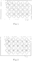
- FIG. 3 discloses a plan view of a capacitive touch circuit pattern in accordance with the present disclosure and combining with FIG 1 and FIG 2 , it can be seen that the present disclosure forms at least two adjacent transparent first-axis electrode blocks 1, a transparent first-axis conductive wire 11, and at least two adjacent transparent second-axis electrode blocks 2 on the surface of a substrate 3.
- the first-axis conductive wire 11 is formed between the two adjacent first-axis electrode blocks 1 to connect the two adjacent first-axis electrode blocks 1.
- the two adjacent second-axis electrode blocks 2 are disposed, respectively, at two sides of the first-axis conductive wire 11, and a second-axis conductive wire 21, which is made of a metal material, connects the two adjacent second-axis electrode blocks 2 and stretches across the first-axis conductive wire 11.
- An insulation spacer 4 is formed between the first-axis conductive wire 11 and the second-axis conductive wire 21 so that the first-axis conductive wire 11 and the second-axis conductive wire 21 are electrically insulated.
- a first-axis surrounding circuit 51 and a second-axis surrounding circuit 52 are respectively formed at two adjacent edges of the substrate 3, wherein the first-axis surrounding circuit 51 connects the first-axis electrode blocks 1, and the second-axis surrounding circuit 52 connects the second-axis electrode blocks 2.
- photolithographic processing can be adopted, the following steps:
- the second-axis conductive wire 21, the first-axis surrounding circuit 51 and, the second-axis surrounding circuit 52 can be made of gold, silver, copper, aluminum or any other metal materials with good conductivity.
- the second-axis conductive wire 21, the first-axis surrounding circuit 51, and the second-axis surrounding circuit 52 can be formed with multiple groups.
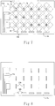
- the second-axis conductive wire 22 can serially connect a plurality of second-axis electrode blocks 2 by a superposition method (as shown in FIG 4 ).
- first-axis electrode blocks 1 and the first-axis conductive wire 11 form a first-axis conductive element 10 and all first-axis conductive elements 10 form a capacitive sensing layer.
- the second-axis electrode blocks 2 and the second-axis conductive wire 21 form a second-axis conductive element 20 and all the second-axis conductive elements 20 form the other capacitive sensing layer.
- the capacitive sensing layers, the insulation spacers 4, and the surrounding circuits 51 and 52 form a touch circuit pattern (as shown in FIG 3 and FIG. 4 ).
- the substrate 3 can be made of glass, plastic or any other transparent insulation material.
- the capacitive touch circuit pattern structure of the present disclosure can be applied to a touch panel of a touch display screen.
- the touch panel comprises a substrate and a capacitive touch circuit pattern structure formed on the substrate in accordance with the present disclosure.
- the touch panel can be superposed on a display panel of the touch display screen.
- the display panel comprises an upper substrate, a lower substrate, a pixel unit disposed between the upper and lower substrates, and a black matrix used for shading light.
- the second conductive wires which are made of non-transparent conductive material in the capacitive touch circuit pattern structure are aligned with the black matrix inside the touch display screen so as to improve transmittance of the light emitted by the display panel.
- the touch circuit pattern structure can be disposed under the upper substrate or above the lower substrate of the display panel so as to use the upper substrate or lower substrate of the display panel as a substrate of the touch panel.
- the second-axis conductive wires 21 and 22 can overlap with a shading layer which is used for shading light and formed by several black matrixes arranged inside the display panel.
- the shading layer can be omitted, using the second-axis conductive wires 21 and 22 as shading elements of the display panel, and the second-axis conductive wires 21 and 22, which are made of a metal material, can reduce the impedance between the second-axis electrode blocks 2 and the second-axis surrounding circuit 52 so as to improve sensitivity of the signal transmission between the electrode blocks and the surrounding circuits.
- the design of arranging the plurality of insulation spacers 4 at intervals as a matrix has the effect of improving the transmittance of the panel.
- first-axis electrode blocks 1 and the second-axis electrode blocks 2 can be formed on the surface of the transparent substrate 3 through a single process.
- the touch circuit pattern can be completed through a third process, which simplifies the photolithographic processing of disposing the touch circuit pattern.
- FIG 7 discloses a plan view of another capacitive touch circuit pattern in accordance with the present disclosure
- disposition form of this circuit pattern is similar to FIG 3 , with the difference being in the order of elements formed on the surface of the substrate.
- photolithographic processing can be adopted, comprising the following steps:
- the first-axis electrode blocks 1a, the second-axis electrode blocks 2a, and the first-axis conductive wire 11a can be respectively formed with multiple groups so that the plurality of first-axis electrode blocks 1a and the second-axis electrode blocks 2a form a touch circuit pattern, and formation and implementing modes of other elements are the same as shown in FIG 1 ⁇ FIG 3 .
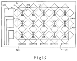
- FIG. 10 discloses a plan view of another capacitive touch circuit pattern in accordance with the present disclosure and combining with FIG 8 and FIG 9 , it can be seen that the present disclosure forms two adjacent first-axis electrode blocks 1b, a first-axis conductive wire 11b and two adjacent second-axis electrode blocks 2b on a substrate 3b.
- the first-axis conductive wire 11b is formed between the two adjacent first-axis electrode blocks 1b to connect the two adjacent first-axis electrode blocks 1b.
- the two adjacent second-axis electrode blocks 2b are disposed respectively at two sides of the first-axis conductive wire 11b.
- the second-axis conductive wire 21b which is made of a metal material, connects the two adjacent second-axis electrode blocks 2b and stretches across the first-axis conductive wire 11b.
- An insulation layer 40b is formed on the surface of the substrate 3b and filled among the first-axis electrode blocks 1b, the second-axis electrode blocks 2b, the first-axis conductive wire 11b, and the second-axis conductive wire 21b so that the first-axis conductive wire 11b and the second-axis conductive wire 21b are electrically insulated.
- a first-axis surrounding circuit 51b and a second-axis surrounding circuit 52b are, respectively, formed at two adjacent edges of the substrate 3b, wherein the first-axis surrounding circuit 51b connects the first-axis electrode blocks 1b and the second-axis surrounding circuit 52b connects the second-axis electrode blocks 2b.
- photolithographic processing can be adopted, comprising the following steps:
- the first-axis electrode blocks 1b, the second-axis electrode blocks 2b, and the first-axis conductive wire 11b can be, respectively, formed with multiple groups so that the plurality of the first-axis electrode blocks 1b and the second-axis electrode blocks 2b form a touch circuit pattern, and formation and implementing modes of other elements are the same as shown in FIG 1 ⁇ FIG 3 .
- FIG. 13 discloses a plan view of another capacitive touch circuit pattern in accordance with the present disclosure
- its disposition form is similar to FIG 10 and the difference is only the order of elements formed on the surface of the substrate.
- photolithographic processing can be adopted, comprising the following steps:
- the second-axis conductive wire 21c, the first-axis surrounding circuit 51c and the second-axis surrounding circuit 52c can be, respectively, formed with multiple groups so that the plurality of first-axis electrode blocks 1c and the second-axis electrode blocks 2c form a touch circuit pattern, and formation and implementing modes of other elements are the same as shown in FIG 8 ⁇ FIG. 10 .
- the second-axis conductive wire, the first-axis surrounding circuit, and the second-axis surrounding circuit can be made of a metal material, according to the present disclosure, the second-axis conductive wire, the first-axis surrounding circuit, and/or the second-axis surrounding circuit can also be made from other non-transparent conductive materials.
Landscapes
- Engineering & Computer Science (AREA)
- General Engineering & Computer Science (AREA)
- Theoretical Computer Science (AREA)
- Human Computer Interaction (AREA)
- Physics & Mathematics (AREA)
- General Physics & Mathematics (AREA)
- Quality & Reliability (AREA)
- Position Input By Displaying (AREA)
Claims (5)
- Ein Touchdisplaybildschirm, der ein Touchpanel umfasst,
wobei das Touchpanel ein Substrat (3) und eine kapazitive Berührungs-Schaltkreis-Musterstruktur umfasst, die auf dem Substrat ausgebildet ist,
wobei die Berührungs-Schaltkreis-Musterstruktur Folgendes umfasst:mindestens eine Gruppe von transparenten ersten Elektrodenblöcken (1), wobei eine jede Gruppe von transparenten ersten Elektrodenblöcken (1) mindestens zwei erste Elektrodenblöcke (1) umfasst, die in Intervallen entlang der Richtung einer ersten Achse angeordnet sind;mindestens eine Gruppe von transparenten ersten leitfähigen Drähten (11), wobei eine jede Gruppe von transparenten ersten leitfähigen Drähten (11) zwischen den benachbarten ersten Elektrodenblöcken (1) in einer selben Gruppe der ersten Elektrodenblöcke (1) angeordnet ist, und verwendet wird, um die ersten Elektrodenblöcke (1) in derselben Gruppe elektrisch zu verbinden;mindestens eine Gruppe von transparenten zweiten Elektrodenblöcken (2), wobei eine jede Gruppe von transparenten zweiten Elektrodenblöcken (2) mindestens zwei zweite Elektrodenblöcke (2) umfasst, die in Intervallen entlang der Richtung einer zweiten Achse angeordnet sind;und wobei die zwei benachbarten zweiten Elektrodenblöcke (2) jeweils an zwei Seiten der mindestens einen Gruppe von ersten leitfähigen Drähten (11) angeordnet sind;mindestens eine Gruppe von zweiten leitfähigen Drähten (21), die aus einem nicht transparenten leitfähigen Material bestehen, wobei eine jede Gruppe von zweiten leitfähigen Drähten (21) zwischen den benachbarten zweiten Elektrodenblöcken (2) in einer selben Gruppe der zweiten Elektrodenblöcke (2) angeordnet sind und verwendet werden, um die zweiten Elektrodenblöcke (2) in derselben Gruppe elektrisch zu verbinden, undeine Isolationsschicht (40), die zwischen den ersten leitfähigen Drähten (11) und den zweiten leitfähigen Drähten (21) ausgebildet ist, sodass die ersten leitfähigen Drähte (11) und die zweiten leitfähigen Drähte (21) elektrisch isoliert sind,wobei die kapazitive Berührungs-Schaltkreis-Musterstruktur ferner einen ersten umgebenden Schaltkreis (51) und einen zweiten umgebenden Schaltkreis (52) an den Rändern der Oberfläche des Substrats (1) umfasst, wobei der erste umgebende Schalkreis (51) elektrisch mit den ersten Elektrodenblöcken (1) verbunden ist und der zweite umgebende Schaltkreis (52) elektrisch mit den zweiten Elektrodenblöcken (2) verbunden ist, dadurch gekennzeichnet, dass die zweiten leitfähigen Drähte (21) in einer selben Gruppe sich in einen Draht erstrecken,und dass die kapazitive Berührungs-Schaltkreis-Musterstruktur des Touchpanels zwischen dem oberen und unteren Substrat eines Anzeige-Panels eines Touchdisplaybildschirms ausgebildet ist, wobei die zweiten leitfähigen Drähte (21) mit einer Schattierungsschicht überlappen, die verwendet wird, um Licht abzufangen und die aus mehreren schwarzen Matrizen gebildet ist, die innerhalb des Anzeigepanels angeordnet sind. - Touchdisplaybildschirm nach Anspruch 1, wobei der erste umgebende Schaltkreis und der zweite umgebende Schaltkreis aus einem nicht transparenten leitfähigen Material bestehen.
- Touchdisplaybildschirm nach Anspruch 1 oder 2, wobei das nicht transparente leitfähige Material ein Metall ist.
- Touchdisplaybildschirm nach Anspruch 3, wobei die Isolationsschicht (40) einen oder mehrere Isolations-Zwischenstücke (4) umfasst, die in Intervallen angeordnet sind, und sich die zweiten leitfähigen Drähte (21) über die entsprechenden Isolations-Zwischenstücke (4) erstrecken.
- Touchdisplaybildschirm nach Anspruch 3, wobei die Isolationsschicht (40) eine integrale Struktur ist, die zumindest einen Teil der ersten Elektrodenblöcke (1) und der zweiten Elektrodenblöcke (2) bedeckt; mindestens ein Paar von durchgängigen Löchern in der Isolationsschicht (40) ausgebildet ist, und das Paar von durchgängigen Löchern an den zwei benachbarten zweiten Elektrodenblöcken (2) in einer selben Gruppe überlagert ist; wobei mindestens ein zweiter leitfähiger Draht (21) zwischen dem Paar von durchgängigen Löchern angeordnet ist und sich auf dem Paar von durchgängigen Löchern erstreckt und diesem überlagert ist, um die zwei benachbarten zweiten Elektrodenblöcke (2) in mindestens einer Gruppe von zweiten Elektrodenblöcken (2) elektrisch zu verbinden.
Applications Claiming Priority (3)
| Application Number | Priority Date | Filing Date | Title |
|---|---|---|---|
| CN2009101295038A CN101840292B (zh) | 2009-03-20 | 2009-03-20 | 电容式触控电路图形及其制法 |
| CN200920006657U CN201374687Y (zh) | 2009-03-20 | 2009-03-20 | 电容式触控电路图形结构 |
| PCT/CN2010/000334 WO2010105507A1 (zh) | 2009-03-20 | 2010-03-19 | 电容式触控电路图形及其制法 |
Publications (3)
| Publication Number | Publication Date |
|---|---|
| EP2410411A1 EP2410411A1 (de) | 2012-01-25 |
| EP2410411A4 EP2410411A4 (de) | 2013-10-02 |
| EP2410411B1 true EP2410411B1 (de) | 2019-03-06 |
Family
ID=42739174
Family Applications (1)
| Application Number | Title | Priority Date | Filing Date |
|---|---|---|---|
| EP10753074.3A Active EP2410411B1 (de) | 2009-03-20 | 2010-03-19 | Kapazitives berührungsschaltungsmuster |
Country Status (5)
| Country | Link |
|---|---|
| US (1) | US10282040B2 (de) |
| EP (1) | EP2410411B1 (de) |
| JP (1) | JP5829206B2 (de) |
| KR (1) | KR101304787B1 (de) |
| WO (1) | WO2010105507A1 (de) |
Families Citing this family (27)
| Publication number | Priority date | Publication date | Assignee | Title |
|---|---|---|---|---|
| JP5418130B2 (ja) * | 2009-10-15 | 2014-02-19 | 大日本印刷株式会社 | 静電容量式タッチパネルセンサおよび当該タッチパネルセンサの製造方法 |
| IT1400933B1 (it) * | 2010-06-21 | 2013-07-02 | St Microelectronics Srl | Touch sensor and method of forming a touch sensor. |
| CN102314271B (zh) * | 2010-07-07 | 2014-11-05 | 宸鸿科技(厦门)有限公司 | 一种电容式触控图形结构及其制法、触控面板及触控显示装置 |
| JP2012068287A (ja) * | 2010-09-21 | 2012-04-05 | Toppan Printing Co Ltd | カラーフィルタ基板及びその製造方法 |
| JP5730551B2 (ja) * | 2010-12-01 | 2015-06-10 | 株式会社ワコム | 指示体による指示位置を検出するための検出センサ、指示体位置検出装置および検出センサの製造方法 |
| CN102081486B (zh) * | 2010-12-21 | 2012-11-28 | 东南大学 | 一种电容式触摸感应器 |
| CN102866794A (zh) | 2011-06-15 | 2013-01-09 | 宸鸿光电科技股份有限公司 | 触控感测层及其制造方法 |
| KR101191949B1 (ko) * | 2011-06-20 | 2012-10-17 | 박준영 | 정전용량 터치 패널의 제조 방법 및 이에 의해 제조되는 터치 패널 |
| CN102955603B (zh) * | 2011-08-17 | 2016-05-25 | 宸鸿科技(厦门)有限公司 | 触控面板及其制造方法 |
| US9612265B1 (en) | 2011-09-23 | 2017-04-04 | Cypress Semiconductor Corporation | Methods and apparatus to detect a conductive object |
| US8903679B2 (en) | 2011-09-23 | 2014-12-02 | Cypress Semiconductor Corporation | Accuracy in a capacitive sense array |
| CN103049144A (zh) | 2011-10-14 | 2013-04-17 | 宸鸿科技(厦门)有限公司 | 触控装置图形及其制造方法 |
| CN103186271B (zh) * | 2011-12-29 | 2016-08-10 | 宸鸿科技(厦门)有限公司 | 触控面板及其制作方法 |
| CN103970311A (zh) * | 2013-01-24 | 2014-08-06 | 联胜(中国)科技有限公司 | 触控板 |
| CN104423674B (zh) * | 2013-09-10 | 2017-09-12 | 宸鸿科技(厦门)有限公司 | 触控面板及其制作方法 |
| US8872526B1 (en) * | 2013-09-10 | 2014-10-28 | Cypress Semiconductor Corporation | Interleaving sense elements of a capacitive-sense array |
| US9495050B1 (en) | 2013-09-10 | 2016-11-15 | Monterey Research, Llc | Sensor pattern with signal-spreading electrodes |
| CN104123036B (zh) * | 2014-06-09 | 2017-02-01 | 京东方科技集团股份有限公司 | 光栅基板及其制作方法、显示装置 |
| KR102375190B1 (ko) * | 2014-11-24 | 2022-03-17 | 삼성디스플레이 주식회사 | 스트레처블 도전 패턴 및 스트레처블 장치 |
| CN104991679B (zh) * | 2015-07-31 | 2018-06-05 | 合肥鑫晟光电科技有限公司 | 触摸基板及其制作方法、触摸显示装置 |
| KR101913395B1 (ko) | 2016-07-29 | 2018-10-31 | 삼성디스플레이 주식회사 | 표시장치 |
| JP6760385B2 (ja) * | 2016-09-14 | 2020-09-23 | ソニー株式会社 | センサ、入力装置および電子機器 |
| KR102438256B1 (ko) * | 2017-06-07 | 2022-08-30 | 엘지디스플레이 주식회사 | 터치 스크린을 갖는 유기 발광 표시 장치 및 이의 제조 방법 |
| KR101964856B1 (ko) | 2017-09-26 | 2019-04-04 | 주식회사 시노펙스 | Lds 공법을 이용한 아이콘 빛 점등용 터치패드 |
| JP2022538698A (ja) * | 2019-03-28 | 2022-09-06 | 京東方科技集團股▲ふん▼有限公司 | タッチ基板、タッチ装置及びタッチ検出方法 |
| KR20210056468A (ko) * | 2019-11-08 | 2021-05-20 | 삼성디스플레이 주식회사 | 센싱 유닛과 그를 포함하는 표시 장치 |
| CN113778261B (zh) * | 2021-09-13 | 2023-09-05 | 武汉华星光电半导体显示技术有限公司 | 可拉伸显示模组及可拉伸显示设备 |
Citations (5)
| Publication number | Priority date | Publication date | Assignee | Title |
|---|---|---|---|---|
| EP1986084A1 (de) * | 2007-04-27 | 2008-10-29 | TPK Touch Solutions Inc. | Leitermusterstruktur eines kapazitiven Berührungsbildschirms |
| US20080264699A1 (en) * | 2007-04-27 | 2008-10-30 | Trendon Touch Technology Corp. | Conductor pattern structure of capacitive touch panel |
| US20080297174A1 (en) * | 2007-05-31 | 2008-12-04 | Sarangan Narasimhan | Capacitive sensing devices |
| CN101359265A (zh) * | 2008-09-10 | 2009-02-04 | 友达光电股份有限公司 | 触控面板、显示器及触控面板的制作方法 |
| CN100495139C (zh) * | 2007-10-10 | 2009-06-03 | 友达光电股份有限公司 | 触控面板及其制作方法 |
Family Cites Families (103)
| Publication number | Priority date | Publication date | Assignee | Title |
|---|---|---|---|---|
| US4028509A (en) | 1975-08-29 | 1977-06-07 | Hughes Aircraft Company | Simplified tabulator keyboard assembly for use in watch/calculator having transparent foldable flexible printed circuit board with contacts and actuator indicia |
| US4233522A (en) | 1978-10-30 | 1980-11-11 | General Electric Company | Capacitive touch switch array |
| JPS57204938A (en) | 1981-06-11 | 1982-12-15 | Fujitsu Ltd | Finger contact type coordinate input device |
| JPS58166437A (ja) | 1982-03-26 | 1983-10-01 | Fujitsu Ltd | 指タツチ式座標検出パネルの製造方法 |
| JPS6075927A (ja) | 1983-09-30 | 1985-04-30 | Fujitsu Ltd | 座標入力装置 |
| US4550221A (en) | 1983-10-07 | 1985-10-29 | Scott Mabusth | Touch sensitive control device |
| US4733222A (en) | 1983-12-27 | 1988-03-22 | Integrated Touch Arrays, Inc. | Capacitance-variation-sensitive touch sensing array system |
| JPS6184729A (ja) | 1984-10-03 | 1986-04-30 | Yamatake Honeywell Co Ltd | 透視形指タツチ入力装置 |
| GB2168816A (en) | 1984-12-19 | 1986-06-25 | Philips Electronic Associated | Touch-sensitive position sensor apparatus |
| US5381160A (en) | 1991-09-27 | 1995-01-10 | Calcomp Inc. | See-through digitizer with clear conductive grid |
| US5543590A (en) | 1992-06-08 | 1996-08-06 | Synaptics, Incorporated | Object position detector with edge motion feature |
| US6239389B1 (en) | 1992-06-08 | 2001-05-29 | Synaptics, Inc. | Object position detection system and method |
| US5880411A (en) | 1992-06-08 | 1999-03-09 | Synaptics, Incorporated | Object position detector with edge motion feature and gesture recognition |
| US7532205B2 (en) | 1992-06-08 | 2009-05-12 | Synaptics, Inc. | Object position detector with edge motion feature and gesture recognition |
| DE69324067T2 (de) | 1992-06-08 | 1999-07-15 | Synaptics Inc | Objekt-Positionsdetektor |
| GB9406702D0 (en) | 1994-04-05 | 1994-05-25 | Binstead Ronald P | Multiple input proximity detector and touchpad system |
| US6114862A (en) | 1996-02-14 | 2000-09-05 | Stmicroelectronics, Inc. | Capacitive distance sensor |
| TW345294U (en) | 1996-06-07 | 1998-11-11 | Mei-Yong Chen | Improved structure for cursor positioned apparatus |
| JPH10171583A (ja) | 1996-12-05 | 1998-06-26 | Wacom Co Ltd | 位置検出装置およびその位置指示器 |
| US6392636B1 (en) | 1998-01-22 | 2002-05-21 | Stmicroelectronics, Inc. | Touchpad providing screen cursor/pointer movement control |
| US7663607B2 (en) | 2004-05-06 | 2010-02-16 | Apple Inc. | Multipoint touchscreen |
| US6188391B1 (en) * | 1998-07-09 | 2001-02-13 | Synaptics, Inc. | Two-layer capacitive touchpad and method of making same |
| US6057903A (en) | 1998-08-18 | 2000-05-02 | International Business Machines Corporation | Liquid crystal display device employing a guard plane between a layer for measuring touch position and common electrode layer |
| US6478976B1 (en) | 1998-12-30 | 2002-11-12 | Stmicroelectronics, Inc. | Apparatus and method for contacting a conductive layer |
| US7030860B1 (en) | 1999-10-08 | 2006-04-18 | Synaptics Incorporated | Flexible transparent touch sensing system for electronic devices |
| GB2367530B (en) | 2000-10-03 | 2003-07-23 | Nokia Mobile Phones Ltd | User interface device |
| JP2002252340A (ja) | 2001-02-26 | 2002-09-06 | Sony Corp | 固体撮像素子 |
| DE10123633A1 (de) | 2001-05-09 | 2003-02-06 | Ego Elektro Geraetebau Gmbh | Sensorelement |
| US6498590B1 (en) | 2001-05-24 | 2002-12-24 | Mitsubishi Electric Research Laboratories, Inc. | Multi-user touch surface |
| JP2003066417A (ja) | 2001-08-22 | 2003-03-05 | Sharp Corp | タッチセンサ一体型表示装置 |
| JP3987729B2 (ja) | 2001-09-11 | 2007-10-10 | シャープ株式会社 | 入出力一体型表示装置 |
| US7477242B2 (en) | 2002-05-20 | 2009-01-13 | 3M Innovative Properties Company | Capacitive touch screen with conductive polymer |
| US7463246B2 (en) | 2002-06-25 | 2008-12-09 | Synaptics Incorporated | Capacitive sensing device |
| US7202859B1 (en) | 2002-08-09 | 2007-04-10 | Synaptics, Inc. | Capacitive sensing pattern |
| US7292229B2 (en) | 2002-08-29 | 2007-11-06 | N-Trig Ltd. | Transparent digitiser |
| US7253808B2 (en) | 2002-11-18 | 2007-08-07 | Lg.Philips Lcd Co., Ltd. | Touch screen system and display device using the same |
| US6970160B2 (en) | 2002-12-19 | 2005-11-29 | 3M Innovative Properties Company | Lattice touch-sensing system |
| US20050030048A1 (en) * | 2003-08-05 | 2005-02-10 | Bolender Robert J. | Capacitive sensing device for use in a keypad assembly |
| US8068186B2 (en) | 2003-10-15 | 2011-11-29 | 3M Innovative Properties Company | Patterned conductor touch screen having improved optics |
| US7382139B2 (en) | 2004-06-03 | 2008-06-03 | Synaptics Incorporated | One layer capacitive sensing apparatus having varying width sensing elements |
| US7394458B2 (en) | 2004-09-24 | 2008-07-01 | Apple Inc. | Low EMI capacitive trackpad |
| US7589713B2 (en) | 2004-10-07 | 2009-09-15 | Alps Electric Co., Ltd. | Capacitive coordinate detection device |
| TWI259409B (en) | 2005-01-07 | 2006-08-01 | Au Optronics Corp | Touch panel for recognizing fingerprint and method of making the same |
| US7952564B2 (en) | 2005-02-17 | 2011-05-31 | Hurst G Samuel | Multiple-touch sensor |
| US7439962B2 (en) | 2005-06-01 | 2008-10-21 | Synaptics Incorporated | Touch pad with flexible substrate |
| GB2428306B (en) | 2005-07-08 | 2007-09-26 | Harald Philipp | Two-dimensional capacitive position sensor |
| TW200709024A (en) | 2005-08-31 | 2007-03-01 | Elan Microelectronics Corp | Touch sensor |
| US7864160B2 (en) | 2005-10-05 | 2011-01-04 | 3M Innovative Properties Company | Interleaved electrodes for touch sensing |
| US20070132737A1 (en) | 2005-12-09 | 2007-06-14 | Mulligan Roger C | Systems and methods for determining touch location |
| US8166649B2 (en) * | 2005-12-12 | 2012-05-01 | Nupix, LLC | Method of forming an electroded sheet |
| US8111243B2 (en) | 2006-03-30 | 2012-02-07 | Cypress Semiconductor Corporation | Apparatus and method for recognizing a tap gesture on a touch sensing device |
| US8144125B2 (en) | 2006-03-30 | 2012-03-27 | Cypress Semiconductor Corporation | Apparatus and method for reducing average scan rate to detect a conductive object on a sensing device |
| US20070229469A1 (en) | 2006-03-31 | 2007-10-04 | Ryan Seguine | Non-planar touch sensor pad |
| US20070229470A1 (en) | 2006-03-31 | 2007-10-04 | Warren Snyder | Capacitive touch sense device having polygonal shaped sensor elements |
| US8264466B2 (en) | 2006-03-31 | 2012-09-11 | 3M Innovative Properties Company | Touch screen having reduced visibility transparent conductor pattern |
| TWI313431B (en) | 2006-04-14 | 2009-08-11 | Ritdisplay Corporatio | Transparent touch panel |
| TWI322374B (en) | 2006-04-14 | 2010-03-21 | Ritdisplay Corp | Light transmission touch panel and manufacturing method thereof |
| CN100530065C (zh) * | 2006-04-20 | 2009-08-19 | 铼宝科技股份有限公司 | 透明触控面板结构 |
| US8004497B2 (en) | 2006-05-18 | 2011-08-23 | Cypress Semiconductor Corporation | Two-pin buttons |
| US8059015B2 (en) | 2006-05-25 | 2011-11-15 | Cypress Semiconductor Corporation | Capacitance sensing matrix for keyboard architecture |
| US8169421B2 (en) | 2006-06-19 | 2012-05-01 | Cypress Semiconductor Corporation | Apparatus and method for detecting a touch-sensor pad gesture |
| US8068097B2 (en) | 2006-06-27 | 2011-11-29 | Cypress Semiconductor Corporation | Apparatus for detecting conductive material of a pad layer of a sensing device |
| US8040321B2 (en) | 2006-07-10 | 2011-10-18 | Cypress Semiconductor Corporation | Touch-sensor with shared capacitive sensors |
| US20080036473A1 (en) | 2006-08-09 | 2008-02-14 | Jansson Hakan K | Dual-slope charging relaxation oscillator for measuring capacitance |
| US20080074398A1 (en) | 2006-09-26 | 2008-03-27 | David Gordon Wright | Single-layer capacitive sensing device |
| US8120584B2 (en) | 2006-12-21 | 2012-02-21 | Cypress Semiconductor Corporation | Feedback mechanism for user detection of reference location on a sensing device |
| US8072429B2 (en) | 2006-12-22 | 2011-12-06 | Cypress Semiconductor Corporation | Multi-axial touch-sensor device with multi-touch resolution |
| US8058937B2 (en) | 2007-01-30 | 2011-11-15 | Cypress Semiconductor Corporation | Setting a discharge rate and a charge rate of a relaxation oscillator circuit |
| US20080180399A1 (en) | 2007-01-31 | 2008-07-31 | Tung Wan Cheng | Flexible Multi-touch Screen |
| US20080231605A1 (en) | 2007-03-21 | 2008-09-25 | Kai-Ti Yang | Compound touch panel |
| JP4506785B2 (ja) | 2007-06-14 | 2010-07-21 | エプソンイメージングデバイス株式会社 | 静電容量型入力装置 |
| JP4998919B2 (ja) * | 2007-06-14 | 2012-08-15 | ソニーモバイルディスプレイ株式会社 | 静電容量型入力装置 |
| TW200901014A (en) * | 2007-06-28 | 2009-01-01 | Sense Pad Tech Co Ltd | Touch panel device |
| CN101349960B (zh) | 2007-07-16 | 2011-05-04 | 张玉辉 | 触控面板装置 |
| TWM344544U (en) * | 2007-12-25 | 2008-11-11 | Cando Corp | Sensory structure of touch panel |
| CN101261379A (zh) | 2008-02-01 | 2008-09-10 | 信利半导体有限公司 | 电容式触摸屏及包含该触摸屏的触摸显示器件 |
| TW200947289A (en) | 2008-05-12 | 2009-11-16 | Tpk Touch Solutions Inc | Layout method of touch circuit pattern |
| CN101587391B (zh) | 2008-05-21 | 2011-06-15 | 宸鸿光电科技股份有限公司 | 触控电路图的制作方法 |
| TWM342558U (en) | 2008-05-26 | 2008-10-11 | Young Fast Optoelectronics Co | Capacitive type touch panel |
| TWM345294U (en) | 2008-05-28 | 2008-11-21 | Young Fast Optoelectronics Co | Structure improvement of capacitive touch panel |
| US8629842B2 (en) * | 2008-07-11 | 2014-01-14 | Samsung Display Co., Ltd. | Organic light emitting display device |
| JP5178379B2 (ja) | 2008-07-31 | 2013-04-10 | 株式会社ジャパンディスプレイイースト | 表示装置 |
| US8711105B2 (en) | 2008-08-21 | 2014-04-29 | Wacom Co., Ltd. | Touchscreen with extended conductive pattern |
| CN102112950B (zh) | 2008-09-12 | 2015-01-28 | 奥博特瑞克斯株式会社 | 电容型触摸面板、显示装置及电容型触摸面板的制造方法 |
| US8493337B2 (en) | 2008-09-22 | 2013-07-23 | Ritfast Corporation | Light transmission touch panel |
| US8816967B2 (en) * | 2008-09-25 | 2014-08-26 | Apple Inc. | Capacitive sensor having electrodes arranged on the substrate and the flex circuit |
| US8624845B2 (en) * | 2008-09-26 | 2014-01-07 | Cypress Semiconductor Corporation | Capacitance touch screen |
| CN201298221Y (zh) | 2008-10-10 | 2009-08-26 | 达虹科技股份有限公司 | 电容式触控面板的二维感测结构 |
| CN101441545A (zh) | 2008-12-08 | 2009-05-27 | 中国南玻集团股份有限公司 | 电容式触控屏及其制造方法 |
| US8274486B2 (en) * | 2008-12-22 | 2012-09-25 | Flextronics Ap, Llc | Diamond pattern on a single layer |
| JP3149113U (ja) | 2008-12-25 | 2009-03-12 | 洋華光電股▲ふん▼有限公司 | キャパシタ式接触制御インダクション構造 |
| JP2010160670A (ja) | 2009-01-08 | 2010-07-22 | Seiko Epson Corp | タッチパネルの製造方法、タッチパネル、表示装置、及び電子機器 |
| CN201374687Y (zh) | 2009-03-20 | 2009-12-30 | 宸鸿科技(厦门)有限公司 | 电容式触控电路图形结构 |
| US9024907B2 (en) | 2009-04-03 | 2015-05-05 | Synaptics Incorporated | Input device with capacitive force sensor and method for constructing the same |
| KR101073333B1 (ko) | 2009-08-27 | 2011-10-12 | 삼성모바일디스플레이주식회사 | 터치 스크린 패널 및 그 제조방법 |
| CN102033669B (zh) | 2009-09-24 | 2013-08-14 | 群康科技(深圳)有限公司 | 电容式触控面板 |
| TWI427520B (zh) | 2009-12-10 | 2014-02-21 | Au Optronics Corp | 觸控顯示面板以及觸控基板 |
| JP5566142B2 (ja) | 2010-03-17 | 2014-08-06 | オートスプライス株式会社 | クリップ端子 |
| KR101100987B1 (ko) | 2010-03-23 | 2011-12-30 | 삼성모바일디스플레이주식회사 | 터치 스크린 패널 |
| KR101040881B1 (ko) | 2010-04-12 | 2011-06-16 | 삼성모바일디스플레이주식회사 | 터치 스크린 패널 |
| KR101448251B1 (ko) | 2010-10-28 | 2014-10-08 | 삼성디스플레이 주식회사 | 터치 스크린 패널 및 이를 구비한 표시 장치 |
| CN102799301B (zh) | 2011-05-28 | 2015-05-20 | 宸鸿科技(厦门)有限公司 | 触控面板的电极结构、制造方法以及触控面板 |
| JP6184729B2 (ja) | 2013-04-17 | 2017-08-23 | 株式会社長谷工コーポレーション | 結合部材 |
-
2010
- 2010-03-19 EP EP10753074.3A patent/EP2410411B1/de active Active
- 2010-03-19 US US13/256,933 patent/US10282040B2/en active Active
- 2010-03-19 KR KR1020107026862A patent/KR101304787B1/ko active IP Right Grant
- 2010-03-19 JP JP2012500043A patent/JP5829206B2/ja active Active
- 2010-03-19 WO PCT/CN2010/000334 patent/WO2010105507A1/zh active Application Filing
Patent Citations (5)
| Publication number | Priority date | Publication date | Assignee | Title |
|---|---|---|---|---|
| EP1986084A1 (de) * | 2007-04-27 | 2008-10-29 | TPK Touch Solutions Inc. | Leitermusterstruktur eines kapazitiven Berührungsbildschirms |
| US20080264699A1 (en) * | 2007-04-27 | 2008-10-30 | Trendon Touch Technology Corp. | Conductor pattern structure of capacitive touch panel |
| US20080297174A1 (en) * | 2007-05-31 | 2008-12-04 | Sarangan Narasimhan | Capacitive sensing devices |
| CN100495139C (zh) * | 2007-10-10 | 2009-06-03 | 友达光电股份有限公司 | 触控面板及其制作方法 |
| CN101359265A (zh) * | 2008-09-10 | 2009-02-04 | 友达光电股份有限公司 | 触控面板、显示器及触控面板的制作方法 |
Also Published As
| Publication number | Publication date |
|---|---|
| WO2010105507A1 (zh) | 2010-09-23 |
| US10282040B2 (en) | 2019-05-07 |
| JP5829206B2 (ja) | 2015-12-09 |
| EP2410411A1 (de) | 2012-01-25 |
| EP2410411A4 (de) | 2013-10-02 |
| JP2012521026A (ja) | 2012-09-10 |
| KR20110000760A (ko) | 2011-01-05 |
| US20120127099A1 (en) | 2012-05-24 |
| KR101304787B1 (ko) | 2013-09-05 |
Similar Documents
| Publication | Publication Date | Title |
|---|---|---|
| EP2410411B1 (de) | Kapazitives berührungsschaltungsmuster | |
| TWI585659B (zh) | 電容式觸控面板及降低電容式觸控面板的金屬導體可見度之觸控面板的製造方法 | |
| JP5512734B2 (ja) | 静電容量式タッチパネルの導電模様構造 | |
| US9454267B2 (en) | Touch sensing circuit and method for making the same | |
| JP5439565B2 (ja) | タッチパネル及びその製造方法 | |
| US8593413B2 (en) | Sensory structure of capacitive touch panel and capacitive touch panel having the same | |
| US20110032207A1 (en) | Capacitive touch sensor | |
| KR101330779B1 (ko) | 터치 패널의 전극 구조, 그 방법 및 터치 패널 | |
| CN101840292B (zh) | 电容式触控电路图形及其制法 | |
| CN103941914B (zh) | 触控面板、触控显示面板及触控信号的感测方法 | |
| EP2650765B1 (de) | Leitermusterstruktur eines kapazitiven Berührungsbildschirms | |
| US9582129B2 (en) | Touch screen panel | |
| CN201741139U (zh) | 触控电路图形结构、触控面板及触控显示屏 | |
| CN104503636A (zh) | 触控模组 | |
| TWI403945B (zh) | Capacitive touch circuit and its manufacturing method | |
| CN102419673A (zh) | 电容式触控电路图形结构及其制法 | |
| TWI640910B (zh) | 顯示面板、電容式觸控電路及其製法 | |
| JP6396815B2 (ja) | 入力装置 | |
| CN104331199A (zh) | 触控电路图形结构及制造方法、触控面板及触控显示屏 |
Legal Events
| Date | Code | Title | Description |
|---|---|---|---|
| PUAI | Public reference made under article 153(3) epc to a published international application that has entered the european phase |
Free format text: ORIGINAL CODE: 0009012 |
|
| 17P | Request for examination filed |
Effective date: 20111014 |
|
| AK | Designated contracting states |
Kind code of ref document: A1 Designated state(s): AT BE BG CH CY CZ DE DK EE ES FI FR GB GR HR HU IE IS IT LI LT LU LV MC MK MT NL NO PL PT RO SE SI SK SM TR |
|
| DAX | Request for extension of the european patent (deleted) | ||
| A4 | Supplementary search report drawn up and despatched |
Effective date: 20130902 |
|
| RIC1 | Information provided on ipc code assigned before grant |
Ipc: G06F 3/044 20060101AFI20130827BHEP |
|
| 17Q | First examination report despatched |
Effective date: 20151119 |
|
| GRAP | Despatch of communication of intention to grant a patent |
Free format text: ORIGINAL CODE: EPIDOSNIGR1 |
|
| STAA | Information on the status of an ep patent application or granted ep patent |
Free format text: STATUS: GRANT OF PATENT IS INTENDED |
|
| INTG | Intention to grant announced |
Effective date: 20180913 |
|
| GRAS | Grant fee paid |
Free format text: ORIGINAL CODE: EPIDOSNIGR3 |
|
| GRAA | (expected) grant |
Free format text: ORIGINAL CODE: 0009210 |
|
| STAA | Information on the status of an ep patent application or granted ep patent |
Free format text: STATUS: THE PATENT HAS BEEN GRANTED |
|
| AK | Designated contracting states |
Kind code of ref document: B1 Designated state(s): AT BE BG CH CY CZ DE DK EE ES FI FR GB GR HR HU IE IS IT LI LT LU LV MC MK MT NL NO PL PT RO SE SI SK SM TR |
|
| REG | Reference to a national code |
Ref country code: GB Ref legal event code: FG4D |
|
| REG | Reference to a national code |
Ref country code: CH Ref legal event code: EP Ref country code: AT Ref legal event code: REF Ref document number: 1105425 Country of ref document: AT Kind code of ref document: T Effective date: 20190315 |
|
| REG | Reference to a national code |
Ref country code: DE Ref legal event code: R096 Ref document number: 602010057397 Country of ref document: DE |
|
| REG | Reference to a national code |
Ref country code: IE Ref legal event code: FG4D |
|
| REG | Reference to a national code |
Ref country code: NL Ref legal event code: FP |
|
| REG | Reference to a national code |
Ref country code: LT Ref legal event code: MG4D |
|
| PG25 | Lapsed in a contracting state [announced via postgrant information from national office to epo] |
Ref country code: SE Free format text: LAPSE BECAUSE OF FAILURE TO SUBMIT A TRANSLATION OF THE DESCRIPTION OR TO PAY THE FEE WITHIN THE PRESCRIBED TIME-LIMIT Effective date: 20190306 Ref country code: LT Free format text: LAPSE BECAUSE OF FAILURE TO SUBMIT A TRANSLATION OF THE DESCRIPTION OR TO PAY THE FEE WITHIN THE PRESCRIBED TIME-LIMIT Effective date: 20190306 Ref country code: FI Free format text: LAPSE BECAUSE OF FAILURE TO SUBMIT A TRANSLATION OF THE DESCRIPTION OR TO PAY THE FEE WITHIN THE PRESCRIBED TIME-LIMIT Effective date: 20190306 Ref country code: NO Free format text: LAPSE BECAUSE OF FAILURE TO SUBMIT A TRANSLATION OF THE DESCRIPTION OR TO PAY THE FEE WITHIN THE PRESCRIBED TIME-LIMIT Effective date: 20190606 |
|
| PG25 | Lapsed in a contracting state [announced via postgrant information from national office to epo] |
Ref country code: BG Free format text: LAPSE BECAUSE OF FAILURE TO SUBMIT A TRANSLATION OF THE DESCRIPTION OR TO PAY THE FEE WITHIN THE PRESCRIBED TIME-LIMIT Effective date: 20190606 Ref country code: GR Free format text: LAPSE BECAUSE OF FAILURE TO SUBMIT A TRANSLATION OF THE DESCRIPTION OR TO PAY THE FEE WITHIN THE PRESCRIBED TIME-LIMIT Effective date: 20190607 Ref country code: LV Free format text: LAPSE BECAUSE OF FAILURE TO SUBMIT A TRANSLATION OF THE DESCRIPTION OR TO PAY THE FEE WITHIN THE PRESCRIBED TIME-LIMIT Effective date: 20190306 Ref country code: HR Free format text: LAPSE BECAUSE OF FAILURE TO SUBMIT A TRANSLATION OF THE DESCRIPTION OR TO PAY THE FEE WITHIN THE PRESCRIBED TIME-LIMIT Effective date: 20190306 |
|
| REG | Reference to a national code |
Ref country code: AT Ref legal event code: MK05 Ref document number: 1105425 Country of ref document: AT Kind code of ref document: T Effective date: 20190306 |
|
| PG25 | Lapsed in a contracting state [announced via postgrant information from national office to epo] |
Ref country code: CZ Free format text: LAPSE BECAUSE OF FAILURE TO SUBMIT A TRANSLATION OF THE DESCRIPTION OR TO PAY THE FEE WITHIN THE PRESCRIBED TIME-LIMIT Effective date: 20190306 Ref country code: RO Free format text: LAPSE BECAUSE OF FAILURE TO SUBMIT A TRANSLATION OF THE DESCRIPTION OR TO PAY THE FEE WITHIN THE PRESCRIBED TIME-LIMIT Effective date: 20190306 Ref country code: PT Free format text: LAPSE BECAUSE OF FAILURE TO SUBMIT A TRANSLATION OF THE DESCRIPTION OR TO PAY THE FEE WITHIN THE PRESCRIBED TIME-LIMIT Effective date: 20190706 Ref country code: ES Free format text: LAPSE BECAUSE OF FAILURE TO SUBMIT A TRANSLATION OF THE DESCRIPTION OR TO PAY THE FEE WITHIN THE PRESCRIBED TIME-LIMIT Effective date: 20190306 Ref country code: EE Free format text: LAPSE BECAUSE OF FAILURE TO SUBMIT A TRANSLATION OF THE DESCRIPTION OR TO PAY THE FEE WITHIN THE PRESCRIBED TIME-LIMIT Effective date: 20190306 Ref country code: SK Free format text: LAPSE BECAUSE OF FAILURE TO SUBMIT A TRANSLATION OF THE DESCRIPTION OR TO PAY THE FEE WITHIN THE PRESCRIBED TIME-LIMIT Effective date: 20190306 Ref country code: IT Free format text: LAPSE BECAUSE OF FAILURE TO SUBMIT A TRANSLATION OF THE DESCRIPTION OR TO PAY THE FEE WITHIN THE PRESCRIBED TIME-LIMIT Effective date: 20190306 |
|
| REG | Reference to a national code |
Ref country code: CH Ref legal event code: PL |
|
| PG25 | Lapsed in a contracting state [announced via postgrant information from national office to epo] |
Ref country code: LU Free format text: LAPSE BECAUSE OF NON-PAYMENT OF DUE FEES Effective date: 20190319 Ref country code: PL Free format text: LAPSE BECAUSE OF FAILURE TO SUBMIT A TRANSLATION OF THE DESCRIPTION OR TO PAY THE FEE WITHIN THE PRESCRIBED TIME-LIMIT Effective date: 20190306 Ref country code: SM Free format text: LAPSE BECAUSE OF FAILURE TO SUBMIT A TRANSLATION OF THE DESCRIPTION OR TO PAY THE FEE WITHIN THE PRESCRIBED TIME-LIMIT Effective date: 20190306 |
|
| REG | Reference to a national code |
Ref country code: BE Ref legal event code: MM Effective date: 20190331 |
|
| REG | Reference to a national code |
Ref country code: DE Ref legal event code: R097 Ref document number: 602010057397 Country of ref document: DE |
|
| PG25 | Lapsed in a contracting state [announced via postgrant information from national office to epo] |
Ref country code: IS Free format text: LAPSE BECAUSE OF FAILURE TO SUBMIT A TRANSLATION OF THE DESCRIPTION OR TO PAY THE FEE WITHIN THE PRESCRIBED TIME-LIMIT Effective date: 20190706 Ref country code: AT Free format text: LAPSE BECAUSE OF FAILURE TO SUBMIT A TRANSLATION OF THE DESCRIPTION OR TO PAY THE FEE WITHIN THE PRESCRIBED TIME-LIMIT Effective date: 20190306 |
|
| PLBE | No opposition filed within time limit |
Free format text: ORIGINAL CODE: 0009261 |
|
| STAA | Information on the status of an ep patent application or granted ep patent |
Free format text: STATUS: NO OPPOSITION FILED WITHIN TIME LIMIT |
|
| PG25 | Lapsed in a contracting state [announced via postgrant information from national office to epo] |
Ref country code: CH Free format text: LAPSE BECAUSE OF NON-PAYMENT OF DUE FEES Effective date: 20190331 Ref country code: MC Free format text: LAPSE BECAUSE OF FAILURE TO SUBMIT A TRANSLATION OF THE DESCRIPTION OR TO PAY THE FEE WITHIN THE PRESCRIBED TIME-LIMIT Effective date: 20190306 Ref country code: IE Free format text: LAPSE BECAUSE OF NON-PAYMENT OF DUE FEES Effective date: 20190319 Ref country code: LI Free format text: LAPSE BECAUSE OF NON-PAYMENT OF DUE FEES Effective date: 20190331 Ref country code: DK Free format text: LAPSE BECAUSE OF FAILURE TO SUBMIT A TRANSLATION OF THE DESCRIPTION OR TO PAY THE FEE WITHIN THE PRESCRIBED TIME-LIMIT Effective date: 20190306 |
|
| 26N | No opposition filed |
Effective date: 20191209 |
|
| PG25 | Lapsed in a contracting state [announced via postgrant information from national office to epo] |
Ref country code: BE Free format text: LAPSE BECAUSE OF NON-PAYMENT OF DUE FEES Effective date: 20190331 Ref country code: SI Free format text: LAPSE BECAUSE OF FAILURE TO SUBMIT A TRANSLATION OF THE DESCRIPTION OR TO PAY THE FEE WITHIN THE PRESCRIBED TIME-LIMIT Effective date: 20190306 |
|
| PG25 | Lapsed in a contracting state [announced via postgrant information from national office to epo] |
Ref country code: TR Free format text: LAPSE BECAUSE OF FAILURE TO SUBMIT A TRANSLATION OF THE DESCRIPTION OR TO PAY THE FEE WITHIN THE PRESCRIBED TIME-LIMIT Effective date: 20190306 |
|
| PG25 | Lapsed in a contracting state [announced via postgrant information from national office to epo] |
Ref country code: MT Free format text: LAPSE BECAUSE OF NON-PAYMENT OF DUE FEES Effective date: 20190319 |
|
| PG25 | Lapsed in a contracting state [announced via postgrant information from national office to epo] |
Ref country code: CY Free format text: LAPSE BECAUSE OF FAILURE TO SUBMIT A TRANSLATION OF THE DESCRIPTION OR TO PAY THE FEE WITHIN THE PRESCRIBED TIME-LIMIT Effective date: 20190306 |
|
| PG25 | Lapsed in a contracting state [announced via postgrant information from national office to epo] |
Ref country code: HU Free format text: LAPSE BECAUSE OF FAILURE TO SUBMIT A TRANSLATION OF THE DESCRIPTION OR TO PAY THE FEE WITHIN THE PRESCRIBED TIME-LIMIT; INVALID AB INITIO Effective date: 20100319 |
|
| PG25 | Lapsed in a contracting state [announced via postgrant information from national office to epo] |
Ref country code: MK Free format text: LAPSE BECAUSE OF FAILURE TO SUBMIT A TRANSLATION OF THE DESCRIPTION OR TO PAY THE FEE WITHIN THE PRESCRIBED TIME-LIMIT Effective date: 20190306 |
|
| PGFP | Annual fee paid to national office [announced via postgrant information from national office to epo] |
Ref country code: NL Payment date: 20230215 Year of fee payment: 14 |
|
| PGFP | Annual fee paid to national office [announced via postgrant information from national office to epo] |
Ref country code: FR Payment date: 20230110 Year of fee payment: 14 |
|
| PGFP | Annual fee paid to national office [announced via postgrant information from national office to epo] |
Ref country code: GB Payment date: 20230126 Year of fee payment: 14 Ref country code: DE Payment date: 20230125 Year of fee payment: 14 |
|
| REG | Reference to a national code |
Ref country code: DE Ref legal event code: R082 Ref document number: 602010057397 Country of ref document: DE Representative=s name: BOEHMERT & BOEHMERT ANWALTSPARTNERSCHAFT MBB -, DE |
|
| PGFP | Annual fee paid to national office [announced via postgrant information from national office to epo] |
Ref country code: NL Payment date: 20240108 Year of fee payment: 15 |