EP2409323B1 - Verfahren zur herstellung einer metallisierung mit mehrfach alternierenden ni- und au-metallisierungsschichten auf mindestens einem kontaktpad auf einem halbleiterwafer - Google Patents
Verfahren zur herstellung einer metallisierung mit mehrfach alternierenden ni- und au-metallisierungsschichten auf mindestens einem kontaktpad auf einem halbleiterwafer Download PDFInfo
- Publication number
- EP2409323B1 EP2409323B1 EP10714596.3A EP10714596A EP2409323B1 EP 2409323 B1 EP2409323 B1 EP 2409323B1 EP 10714596 A EP10714596 A EP 10714596A EP 2409323 B1 EP2409323 B1 EP 2409323B1
- Authority
- EP
- European Patent Office
- Prior art keywords
- metallization
- layer
- contact pad
- wafer
- semiconductor wafer
- Prior art date
- Legal status (The legal status is an assumption and is not a legal conclusion. Google has not performed a legal analysis and makes no representation as to the accuracy of the status listed.)
- Not-in-force
Links
Images


Classifications
-
- H—ELECTRICITY
- H10—SEMICONDUCTOR DEVICES; ELECTRIC SOLID-STATE DEVICES NOT OTHERWISE PROVIDED FOR
- H10W—GENERIC PACKAGES, INTERCONNECTIONS, CONNECTORS OR OTHER CONSTRUCTIONAL DETAILS OF DEVICES COVERED BY CLASS H10
- H10W72/00—Interconnections or connectors in packages
- H10W72/20—Bump connectors, e.g. solder bumps or copper pillars; Dummy bumps; Thermal bumps
-
- H—ELECTRICITY
- H10—SEMICONDUCTOR DEVICES; ELECTRIC SOLID-STATE DEVICES NOT OTHERWISE PROVIDED FOR
- H10W—GENERIC PACKAGES, INTERCONNECTIONS, CONNECTORS OR OTHER CONSTRUCTIONAL DETAILS OF DEVICES COVERED BY CLASS H10
- H10W72/00—Interconnections or connectors in packages
- H10W72/01—Manufacture or treatment
- H10W72/012—Manufacture or treatment of bump connectors, dummy bumps or thermal bumps
-
- H—ELECTRICITY
- H10—SEMICONDUCTOR DEVICES; ELECTRIC SOLID-STATE DEVICES NOT OTHERWISE PROVIDED FOR
- H10W—GENERIC PACKAGES, INTERCONNECTIONS, CONNECTORS OR OTHER CONSTRUCTIONAL DETAILS OF DEVICES COVERED BY CLASS H10
- H10W72/00—Interconnections or connectors in packages
- H10W72/01—Manufacture or treatment
- H10W72/012—Manufacture or treatment of bump connectors, dummy bumps or thermal bumps
- H10W72/01251—Changing the shapes of bumps
- H10W72/01255—Changing the shapes of bumps by using masks
-
- H—ELECTRICITY
- H10—SEMICONDUCTOR DEVICES; ELECTRIC SOLID-STATE DEVICES NOT OTHERWISE PROVIDED FOR
- H10W—GENERIC PACKAGES, INTERCONNECTIONS, CONNECTORS OR OTHER CONSTRUCTIONAL DETAILS OF DEVICES COVERED BY CLASS H10
- H10W72/00—Interconnections or connectors in packages
- H10W72/01—Manufacture or treatment
- H10W72/019—Manufacture or treatment of bond pads
-
- H—ELECTRICITY
- H10—SEMICONDUCTOR DEVICES; ELECTRIC SOLID-STATE DEVICES NOT OTHERWISE PROVIDED FOR
- H10W—GENERIC PACKAGES, INTERCONNECTIONS, CONNECTORS OR OTHER CONSTRUCTIONAL DETAILS OF DEVICES COVERED BY CLASS H10
- H10W72/00—Interconnections or connectors in packages
- H10W72/071—Connecting or disconnecting
- H10W72/072—Connecting or disconnecting of bump connectors
- H10W72/07251—Connecting or disconnecting of bump connectors characterised by changes in properties of the bump connectors during connecting
-
- H—ELECTRICITY
- H10—SEMICONDUCTOR DEVICES; ELECTRIC SOLID-STATE DEVICES NOT OTHERWISE PROVIDED FOR
- H10W—GENERIC PACKAGES, INTERCONNECTIONS, CONNECTORS OR OTHER CONSTRUCTIONAL DETAILS OF DEVICES COVERED BY CLASS H10
- H10W72/00—Interconnections or connectors in packages
- H10W72/20—Bump connectors, e.g. solder bumps or copper pillars; Dummy bumps; Thermal bumps
- H10W72/29—Bond pads specially adapted therefor
-
- H—ELECTRICITY
- H10—SEMICONDUCTOR DEVICES; ELECTRIC SOLID-STATE DEVICES NOT OTHERWISE PROVIDED FOR
- H10W—GENERIC PACKAGES, INTERCONNECTIONS, CONNECTORS OR OTHER CONSTRUCTIONAL DETAILS OF DEVICES COVERED BY CLASS H10
- H10W72/00—Interconnections or connectors in packages
- H10W72/90—Bond pads, in general
- H10W72/921—Structures or relative sizes of bond pads
- H10W72/923—Bond pads having multiple stacked layers
-
- H—ELECTRICITY
- H10—SEMICONDUCTOR DEVICES; ELECTRIC SOLID-STATE DEVICES NOT OTHERWISE PROVIDED FOR
- H10W—GENERIC PACKAGES, INTERCONNECTIONS, CONNECTORS OR OTHER CONSTRUCTIONAL DETAILS OF DEVICES COVERED BY CLASS H10
- H10W72/00—Interconnections or connectors in packages
- H10W72/90—Bond pads, in general
- H10W72/931—Shapes of bond pads
- H10W72/934—Cross-sectional shape, i.e. in side view
-
- H—ELECTRICITY
- H10—SEMICONDUCTOR DEVICES; ELECTRIC SOLID-STATE DEVICES NOT OTHERWISE PROVIDED FOR
- H10W—GENERIC PACKAGES, INTERCONNECTIONS, CONNECTORS OR OTHER CONSTRUCTIONAL DETAILS OF DEVICES COVERED BY CLASS H10
- H10W72/00—Interconnections or connectors in packages
- H10W72/90—Bond pads, in general
- H10W72/951—Materials of bond pads
- H10W72/952—Materials of bond pads comprising metals or metalloids, e.g. PbSn, Ag or Cu
Definitions
- the present invention relates to a method for producing a metallization for at least one contact pad with the features mentioned in claim 1, in particular the present invention relates to an improved technology for producing contact areas (contact pads) with a metallization, also known as under bump metallization (UBM). for the electrical connection between semiconductor structures and another connection partner.
- UBM under bump metallization
- the flip-chip assembly (also reversible assembly) is understood to be a method for contacting contact pads of unhoused semiconductor chips (also wafers, semiconductor wafers) by means of contact bumps.
- the flip chip technology is e.g. used in the manufacture of complex microprocessors.
- the chip In the flip-chip assembly, the chip is mounted directly, with no additional connecting wires, with the active contact side down - towards the circuit carrier. This leads to particularly small dimensions of the housing and short conductor lengths. In the case of very complex circuits, this technology often offers the only sensible connection option, because in some cases several thousand contacts have to be implemented. In this way, the entire surface of the semiconductor chip can be used for contacting. With flip-chip bonding technology, all contacts are connected simultaneously.
- solder In the flip-chip assembly, a metal or metal mixture, the solder, is deposited on the semiconductor chip or wafer or a printed circuit board. This creates thousands of soldering bodies that are cylindrical or spherical, depending on the placement process. These solder bodies are located exactly on the contact points, which establish the connection to the circuit structures in the deeper layers of the wafer (semiconductor chips). The solder bodies are then remelted into small balls in the reflow process, creating a good adhesive, electrically good conductive connection between the solder body and the chip-side metallization (under bump metallization) and a eutectic solder body is given a quasi-spherical surface. These solder balls are also called "bumps".
- under bump metallization a metallization (so-called “under bump metallization”) is often used, which the mechanical
- Another method of bumping a wafer is by stencil printing. After having received a solderable surface on the pads by means of electroplating, the wafer is printed with solder paste in a stencil printer. Afterwards, the wafer is also subjected to a reflow process, the solder paste melts and bumps occur. The wafer can then be cleaned to remove excess flux residue, if necessary.
- electroless plating for producing a metallization.
- electroless nickel phosphorus and then electroless gold are deposited on an Al pad after a corresponding pretreatment (e.g. zincate treatment) in appropriate chemical baths.
- the standard technology for assembling the (regularly tin-containing) flip-chip solder bumps requires a few micrometers thick nickel layer as UBM, which is necessary to reduce the consumption of nickel due to the formation of a NiSn-IMC (intermetallic compound), e.g. Ni 3 Sn 4 , to compensate during the soldering process.
- a nickel layer which is a few micrometers thick, is conventionally produced by means of galvanic or electroless plating, as already described in more detail.
- a complete dry deposition (sputtering / vapor deposition) of a nickel layer with a thickness in the micrometer range is not possible, however, since such a layer leads to a high intrinsic mechanical stress and therefore has too little adhesion.
- DE 103 22 135 A1 describes a component with a solder connection between a first partial body with a first flat metallization and a second partial body with a second flat metallization, the solder connection comprising a solder body made of a reflowable solder, in which at least one of the first and second flat Metallization comprises a nanocrystalline layer on the surface facing the solder body.
- US 2006/0284313 A1 uses a shape-memory material as an under bump metallization, which can consist of an alloy of titanium and nickel.
- UBM metallization
- a contact pad of a semiconductor chip A disadvantage of the aforementioned technologies for producing a metallization (UBM) for a contact pad of a semiconductor chip is the use of wet chemical processes, which in many cases are associated with the use of toxic or at least potentially corrosive baths (e.g. cyanide bath for Au deposition). Furthermore, currentless deposition on III / V semiconductors can lead to game deposition depending on the current design of the surface.
- US 2007/0045848 A1 describes a wafer structure with a semiconductor substrate, a number of UBM layers and a number of bumps, the UBM layer having a layer structure of two multiply alternating Ni and Cu metallization layers.
- DE 1 439 527 A1 discloses a method for contacting semiconductor devices and relates to metal plating contacts with multiple alternating, electrolessly plated Au and Ni layers.
- JPH 10 163 590 A. relates to a method of forming a stack of twice alternating electroplated Au and Ni layers for C-4 thin film metallurgy.
- the method according to the invention for producing a metallization (UBM) for at least one contact pad has the following method steps: applying at least one contact pad to a semiconductor wafer, applying a barrier layer to the top of the at least one contact pad, applying a metallization to the top of the barrier layer, the barrier layer and the metallization (and preferably also the contact pad) by means of physical vapor deposition (physical vapor deposition, hereinafter also referred to as PVD) are applied and the metallization is formed as a layer structure of two, multiple alternating metallization layers, the first metallization layer being formed from nickel and the second metallization layer from gold, the first metallization layer being formed with a layer thickness of less than 100 nm, the second metallization layer with a layer thickness between 30 nm and 50 nm is formed and the sum of the layer thicknesses of the first metallization layers is greater than 1 ⁇ m.
- PVD physical vapor deposition
- the invention thus enables the production of a Ni-based UBM exclusively by means of PVD processes (preferably sputtering and vapor deposition).
- PVD processes preferably sputtering and vapor deposition.
- the problem of the high intrinsic voltages of Ni layers in PVD deposits is solved in that after the deposition of a comparatively thin Ni layer (layer thickness less than 100 nm), a layer of a ductile, electrically conductive material, namely gold, follows.
- Ni instead of Ni, a Ni alloy can also be used, which preferably contains at least 10% nickel (by mass).
- the barrier layer is preferably designed to prevent the diffusion of metal atoms from the contact pad into the UBM and possibly further into the solder bump.
- the barrier layer preferably consists of an amorphous or finely crystalline metallization or intermetallic compound provided with decorated grain boundaries, which does not react chemically with the metallization of the contact pad or the UBM. Intermetallic compounds such as WSiN, TiW, TiMo or others preferably come in here Question.
- the barrier layer preferably has a layer thickness between 50 nm and 1 ⁇ m.
- the first metallization layer consists of Ni or, in an example not belonging to the claimed subject matter, of a Ni alloy (for example NiV).
- This metallization is responsible for the electrical and metallurgical mechanical properties of the bump-UBM connection and must be adapted to the metallurgy of the bump itself.
- Ni or, in an example not belonging to the claimed subject matter is suitable.
- the first of Ni has a thickness of less than 100 nm.
- the second metallization layer consists of gold.
- the second metallization layer can consist of a metal from the group silver, platinum, copper, iron, aluminum, zinc, tin and lead, a mixture of at least two metals from the group gold, silver, platinum, copper, iron , Aluminum, zinc, tin and lead or an alloy of the last-mentioned metals, in which case the second metallization layer is preferably made of a material with a ductility which corresponds to at least 60% of the ductility of gold and an electrical conductivity which is at least 60% of corresponds to electrical conductivity of gold, and is preferably formed with a layer thickness between 10-100 nm.
- the contact pad is preferably also applied by means of physical deposition.
- the contact pad is preferably applied by vapor deposition and the barrier layer by sputtering.
- the first metallization layer made of nickel is formed with a layer thickness of less than 100 nm.
- the second metallization layer made of gold is formed with a layer thickness between 30-50 nm.
- the contact pad is preferably with an area between 1 ⁇ m 2 and 0.20 m 2 (corresponds to 450 mm wafer diameter), the first metallization layer with an area between 1 ⁇ m 2 and 0.20 m 2 and the second metallization layer with an area between 1 ⁇ m 2 and 0.20 m 2 , an area between 0.01 and 0.1 is particularly preferred in each case mm 2 .
- a tin-containing solder bump can be used for subsequent contacting by means of flip-chip assembly.
- the semiconductor wafer has at least one contact pad arranged on the semiconductor wafer (preferably several 1000 contact pads, the contact pads preferably being the electrical connection of the semiconductor wafer having a microelectronic circuit to the outside), wherein a barrier layer is provided on the top of the at least one contact pad and a metallization structure is arranged on the top of the barrier layer, the metallization structure according to the invention having two, multiple alternating metallization layers, the the first metallization layer is made of nickel with a layer thickness of less than 100 nm and the second metallization layer is made of an electrically conductive, ductile material different from nickel, namely gold.
- the barrier layer preferably completely covers the contact pad located on the wafer.
- the metallization structure preferably covers at least 50% of the surface of the contact pad (barrier layer in between) - particularly preferably at least 80% of the surface of the contact pad.
- the number of successive stacks of the first metallization layer and the second metallization layer is selected such that the sum of the layer thicknesses of the first metallization layers is greater than 1 ⁇ m (more preferably greater than 3 ⁇ m).
- the semiconductor wafer preferably has a semiconductor chip and / or the semiconductor wafer has at least one microelectronic circuit.
- the semiconductor wafer with the above.
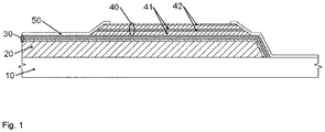
- Fig. 1 shows a wafer with a metallization structure produced according to the invention in a schematic, sectional representation.
- the wafer 10 may comprise a chip or an electronic circuit, for example.
- the wafer 10 In order to contact this electronic circuit of the wafer 10 (also referred to as substrate or semiconductor wafer) with a circuit carrier, the wafer 10 has a multiplicity of contact pads 20, via which the electronic circuit of the wafer 10 exchanges (communicates) electrical signals with the circuit carrier.
- the contact pads 20 can be applied, for example, from ductile material such as Al, Cu or Au by vapor deposition (e-beam evaporation) with the aid of a mask 11 ( 3 and 4 ).
- solder bump (not shown here) is applied between the contact pads 20 and the contacts of the circuit carrier and subsequently wafers 10 and circuit carriers permanently soldered together.
- a barrier layer 30 is first applied to the contact pad 20 by means of sputtering. This can be done as in 5 and 6 represented by the same mask 11 as when applying the pads 20.
- the method has the additional advantage that the pad metallization is completely surrounded by a diffusion barrier and therefore additionally shows a higher electromigration resistance at high current densities in the metallization.
- Fundamentally different deposition properties are used for the contact pads 20 and the barrier layer 30: vapor deposition the contact pads 20 has an isotropic behavior and the sputtering of the barrier layer 30 has an anisotropic behavior.
- Fig. 7a shows the deposition of alternating metal layers 41, 42 produced, for example, by electron beam evaporation.
- the metallization structure 40 covers the entire contact area 20 by using the same mask 11 as for the deposition of the contact pad 20.
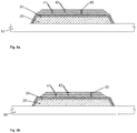
- the resulting structures after deposition of the alternating layer sequence 41, 42 is shown in FIGS 8a and 8b shown.
- the problem of the high intrinsic stresses of Ni layers in PVD deposits is solved according to the invention in that after the deposition of a thin Ni layer (layer thickness less than 100 nm) a layer made of a ductile, electrically conductive material, namely gold with a layer thickness of 30-50 nm follows.
- the interruption of the Ni layer 41 by the Au layer 42 means that the subsequent Ni layer 41 has no or a significantly reduced initial mechanical stress.
- This method advantageously enables the production of a mechanically and electrically reliable UBM without the use of wet chemical processes.
- a passivation layer 50 is preferably applied ( Fig. 1 ) that cover the side areas of the Layer stack 41, 42 covers and the contact surface defines the solder bump (not shown here).
Landscapes
- Internal Circuitry In Semiconductor Integrated Circuit Devices (AREA)
- Wire Bonding (AREA)
- Physical Vapour Deposition (AREA)
- Electrodes Of Semiconductors (AREA)
Description
- Die vorliegende Erfindung betrifft ein Verfahren zur Herstellung einer Metallisierung für mindestens ein Kontaktpad mit den im Anspruch 1 genannten Merkmalen, insbesondere betrifft die vorliegende Erfindung eine verbesserte Technologie zur Herstellung von Kontaktflächen (Kontaktpads) mit einer Metallisierung, auch sog. under bump metallization (UBM) zur elektrischen Verbindung zwischen Halbleiterstrukturen und einem weiteren Verbindungspartner.
- Unter der Flip-Chip-Montage (auch Wende-Montage) wird ein Verfahren zur Kontaktierung von Kontaktpads ungehäuster Halbleiter-Chips (auch Wafer, Halbleiterwafer) mittels Kontaktierhügel - sogenannten "Bumps" verstanden. Die Flip-Chip-Technologie wird z.B. bei der Herstellung komplexer Mikroprozessoren verwendet. Bei der Flip-Chip-Montage wird der Chip direkt, ohne weitere Anschlussdrähte, mit der aktiven Kontaktierungsseite nach unten - zum Schaltungsträger hin - montiert. Dies führt zu besonders geringen Abmessungen des Gehäuses und kurzen Leiterlängen. Bei sehr komplexen Schaltkreisen bietet diese Technologie oft die einzige sinnvolle Verbindungsmöglichkeit an, weil zum Teil mehrere tausend Kontakte realisiert werden müssen. So kann die gesamte Fläche des Halbleiter-Chips zur Kontaktierung genutzt werden. Bei der Flip-Chip-Bondtechnik erfolgt die Verbindung aller Kontakte gleichzeitig.
- Bei der Flip-Chip-Montage wird ein Metall oder Metallgemisch, das Lot, auf den Halbleiterchip oder Wafer oder eine Leiterplatte abgeschieden. Dadurch entstehen tausende mit je nach Platzierungsverfahren zylindrischen oder kugelförmigen Lotkörpern. Diese Lotkörper befinden sich jeweils exakt auf den Kontaktpunkten, welche die Verbindung zu den Schaltungsstrukturen in den tieferen Schichten des Wafers (Halbleiter-Chips) herstellen. Die Lotkörper werden anschließend zu kleinen Kugeln im Reflowverfahren umgeschmolzen, wobei eine gut haftende, elektrisch gut leitfähige Verbindung zwischen dem Lotkörper und der chipseitigen Metallisierung (Under bump metallization) entsteht und ein eutektischer Lotkörper eine quasi halbkugelförmige Oberfläche erhält. Diese Lotkugeln werden auch "Bumps" genannt.
- Zwischen Kontaktierhügel (Bump) und Kontaktpad des Halbleiter-Chips wird häufig eine Metallisierung (sog. "under bump metallization") verwendet, die die mechanische
- Belastbarkeit der Verbindung zwischen Bump und Kontaktpad erhöht. Weiterhin erfüllt die Metallisierung häufig die Aufgabe, die Diffusion von Metallatomen des Kontaktpads in den Bump zu unterbinden, was anderenfalls zu einer Destabilisierung der Verbindung führen würden.
- Eine weitere Methode, um einen Wafer mit "Bumps" zu versehen, ist der Schablonendruck. Der Wafer wird, nachdem er mittels Galvanik eine lötbare Oberfläche an den Pads erhalten hat, in einem Schablonendrucker mit Lotpaste bedruckt. Danach wird der Wafer auch hier einem Reflowprozess unterzogen, die Lotpaste schmilzt und es entstehen Bumps. Anschließend kann der Wafer gereinigt werden, um überflüssige Flussmittelreste zu entfernen, falls dies notwendig sein sollte.
- Es ist bekannt, die Metallisierung durch vollflächige Abscheidung einer Diffusionsbarriere mittels Sputtern, anschließendem Sputtern einer dünnen Startschicht für einen nachfolgenden galvanischen Prozess, lithografische Strukturierung (positiv) und galvanische Abscheidung einer 5-10 µm dicken UBM-Schicht herzustellen. Danach erfolgt eine Ätzung der Diffusionsbarriere und der Startschicht.
- Alternativ ist zur Herstellung einer Metallisierung die Verwendung einer außenstromlosen Abscheidung bekannt. In diesem Fall wird auf einem Al-Pad nach einer entsprechenden Vorbehandlung (z.B. Zinkatbehandlung) stromlos Nickel-Phosphor und danach stromlos Gold in entsprechenden chemischen Bädern abgeschieden.
- Die Standardtechnologie für die Montage der (regelmäßig zinnhaltigen) Flip-Chip Lot-Bumps erfordert eine einige Mikrometer dicke Nickelschicht als UBM, die notwendig ist, um den Verbrauch von Nickel infolge der Bildung einer NiSn-IMC (intermetallic compound), z.B. Ni3Sn4, während des Lötprozesses zu kompensieren. Eine solche einige Mikrometer dicke Nickelschicht wird, wie bereits näher beschrieben, herkömmlicherweise mittels galvanischer oder stromloser Abscheidung hergestellt. Eine vollständige Trockenabscheidung (Sputtern/Bedampfen) einer Nickelschicht mit einer Dicke im Mikrometerbereich ist jedoch nicht möglich, da eine solche Schicht zu einer hohen intrinsischen mechanischen Spannung führt und daher eine zu geringe Adhäsion aufweist.
-
DE 103 22 135 A1 beschreibt ein Bauelement mit einer Lötverbindung zwischen einem ersten Teilkörper mit einer ersten flächigen Metallisierung und einem zweiten Teilkörper mit einer zweiten flächigen Metallisierung, wobei die Lötverbindung einen Lotkörper aus einem aufschmelzbaren Lot umfasst, bei dem zumindest eine aus erster und zweiter flächiger Metallisierung auf der zum Lotkörper weisenden Oberfläche eine nanokristalline Schicht umfasst. -
US 2006/0284313 A1 verwendet als under bump metallization ein Material mit Formgedächtnis, das aus einer Legierung von Titan und Nickel bestehen kann. - Nachteilig an den vorgenannten Technologien zur Herstellung einer Metallisierung (UBM) für ein Kontaktpad eines Halbleiter-Chips ist die Verwendung nasschemischer Prozesse, die in vielen Fällen mit Verwendung toxischer oder zumindest potentiell korrosiver Bäder (z.B. Cyanidbad bei Au-Abscheidung) verbunden sind. Weiterhin kann die stromlose Abscheidung auf III/V-Halbleitern in Abhängigkeit von der aktuellen Gestaltung der Oberfläche zu Wildabscheidungen führen.
-
US 2007/0045848 A1 beschreibt eine Waferstruktur mit einem Halbleitersubstrat, einer Anzahl von UBM-Schichten und einer Anzahl von Bumps, wobei die UBM-Schicht eine Schichtstruktur zweier mehrfach alternierender Ni- und Cu-Metallisierungsschichten aufweist.DE 1 439 527 A1 offenbart ein Verfahren zum Kontaktieren von Halbleiteranordnungen und betrifft Metall-Plattierungskontakte mit mehrfach alternierenden, stromlos plattierten Au- und Ni-Schichten.JPH 10 163 590 A - Es ist daher Aufgabe der vorliegenden Erfindung, ein Verfahren zur Herstellung eines Halbleiterwafers mit einer UBM-Metallisierung anzugeben, die einerseits mittels physikalischer Gasphasenabscheidung (Trockenabscheidung) hergestellt wird und andererseits eine ausreichend hohe Adhäsion eines Lot-Bumps gewährleistet.
- Diese Aufgaben werden erfindungsgemäß durch ein Verfahren zur Herstellung eines Halbleiterwafers mit den im Patentanspruch 1 genannten Merkmalen gelöst. Bevorzugte Ausgestaltungen der Erfindung sind in den Unteransprüchen enthalten.
- Das erfindungsgemäße Verfahren zur Herstellung einer Metallisierung (UBM) für mindestens ein Kontaktpad weist folgende Verfahrensschritte auf: Aufbringen mindestens eines Kontaktpads auf einen Halbleiterwafer, Aufbringen einer Barriereschicht auf die Oberseite des mindestens einen Kontaktpads, Aufbringen einer Metallisierung auf die Oberseite der Barriereschicht, wobei die Barriereschicht und die Metallisierung (und vorzugsweise auch das Kontaktpad) mittels physikalischer Gasphasenabscheidung (physical vapour deposition, nachfolgend auch als PVD bezeichnet) aufgebracht werden und die Metallisierung als Schichtstruktur zweier, mehrfach alternierender Metallisierungsschichten ausgebildet wird, wobei die erste Metallisierungsschicht aus Nickel und die zweite Metallisierungsschicht aus Gold ausgebildet wird, die erste Metallisierungsschicht mit einer Schichtdicke kleiner als 100 nm ausgebildet wird, die zweite Metallisierungsschicht mit einer Schichtdicke zwischen 30 nm und 50 nm ausgebildet wird und die Summe der Schichtdicken der ersten Metallisierungsschichten größer als 1 µm beträgt.
- Die Erfindung ermöglicht damit die Herstellung einer Ni-basierten UBM ausschließlich mittels PVD-Verfahren (vorzugsweise Sputtern und Aufdampfen). Das Problem der hohen intrinsischen Spannungen von Ni-Schichten bei PVD-Abscheidungen wird dadurch gelöst, dass nach der Abscheidung einer vergleichsweise dünnen Ni-Schicht (Schichtdicke kleiner als 100 nm) eine Schicht aus einem duktilen, elektrisch leitfähigen Material, nämlich Gold, folgt. Diese beiden Schritte (Aufbringen einer Ni-Schicht und einer Schicht aus einem duktilen, elektrisch leitfähigen Material, nämlich Gold) werden erfindungsgemäß mehrmals wiederholt, was zu einem Stapel alternierender Ni-Schichten und Schichten aus dem duktilen, elektrisch leitfähigen Material, nämlich Gold, mit einer Gesamtdicke von einigen Mikrometern (größer 1 µm, noch bevorzugter größer 2 µm) führt. Dieses Verfahren ermöglicht vorteilhafterweise die Herstellung einer mechanisch und elektrisch zuverlässigen UBM ohne Verwendung nasschemischer Prozesse.
- In einem zum beanspruchten Gegenstand nicht gehörenden Beispiel kann auch anstatt Ni eine Ni-Legierung benutzt werden, die vorzugsweise mindestens 10% Nickel (bezogen auf die Masse) enthält.
- Die Barriereschicht ist vorzugsweise ausgebildet um die Diffusion von Metallatomen aus dem Kontaktpad in die UBM und eventuell weiter in das Lot-Bump zu verhindern. Die Barriereschicht besteht vorzugsweise aus einer amorphen oder feinkristallinen mit dekorierten Korngrenzen versehenen Metallisierung oder intermetallischen Verbindung , die chemisch nicht mit der Metallisierung des Kontaktpads oder der UBM reagiert. Es kommen hier vorzugsweise intermetallische Verbindungen wie WSiN, TiW, TiMo oder andere in Frage. Die Barriereschicht weist vorzugsweise eine Schichtdicke zwischen 50 nm und 1 µm auf.
- Die erste Metallisierungsschicht besteht erfindungsgemäß aus Ni oder in einem zum beanspruchten Gegenstand nicht gehörenden Beispiel aus einer Ni-Legierung (z.B. NiV). Diese Metallisierung ist in metallurgischer Hinsicht verantwortlich für die elektrischen und mechanischen Eigenschaften der Bump-UBM Verbindung und muss an die Metallurgie des Bumps selbst angepasst sein. Für PbSn Bumps ist beispielsweise Ni oder, in einem zum beanspruchten Gegenstand nicht gehörenden Beispiel, geeignet. Die erste aus Ni weist eine Dicke kleiner als 100 nm auf.
- Da Metalle entsprechend der ersten Metallisierung, in der Regel eine sehr hohe mechanische Verspannung aufweisen, wenn sie im physikalischen Abscheidungsverfahren aufgebracht werden, muss alternierend eine zweite Metallisierung mit eingebaut werden, die diese Verspannungen aufnehmen kann, die Metallurgie und elektrische Leitfähigkeit des Bump-UBM-Systems nicht negativ beeinflusst. Die zweite Metallisierungsschicht besteht erfindungsgemäß aus Gold. In nicht zum beanspruchten Gegenstand gehörenden Beispielen kann die zweite Metallisierungsschicht aus einem Metall aus der Gruppe Silber, Platin, Kupfer, Eisen, Aluminium, Zink, Zinn und Blei, einer Mischung mindestens zwei Metalle aus der Gruppe Gold, Silber, Platin, Kupfer, Eisen, Aluminium, Zink, Zinn und Blei oder einer Legierung der zuletzt genannten Metalle bestehen, wobei dann die zweite Metallisierungsschicht vorzugsweise aus einem Material mit einer Duktilität, die mindestens 60% der Duktilität von Gold entspricht, und einer elektrischen Leitfähigkeit, die mindestens 60% der elektrischen Leitfähigkeit von Gold entspricht, und vorzugsweise mit einer Schichtdicke zwischen 10-100 nm ausgebildet wird.
- Vorzugsweise wird auch das Kontaktpad mittels physikalischer Abscheidung aufgebracht. Vorzugsweise werden das Kontaktpad durch Aufdampfen und die Barriereschicht durch Sputtern aufgebracht.
- Die erste Metallisierungsschicht aus Nickel wird mit einer Schichtdicke kleiner als 100 nm ausgebildet. Die zweite Metallisierungsschicht aus Gold wird mit einer Schichtdicke zwischen 30-50 nm ausgebildet.
- Vorzugsweise wird das Kontaktpad mit einer Fläche zwischen 1 µm2 und 0,20 m2 (entspricht 450 mm Waferdurchmesser), die erste Metallisierungsschicht mit einer Fläche zwischen 1 µm2 und 0,20 m2 und die zweite Metallisierungsschicht mit einer Fläche zwischen 1 µm2 und 0,20m2 ausgebildet, besonders bevorzugt ist jeweils eine Fläche zwischen 0,01 und 0,1 mm2.
- Erfindungsgemäß kann ein zinnhaltiges Lot-Bump zur späteren Kontaktierung mittels Flip-Chip-Montage verwendet werden.
- Der Halbleiterwafer weist mindestens ein auf dem Halbleiterwafer angeordnetes Kontaktpad (vorzugsweise mehrere 1000 Kontaktpads auf, wobei die Kontaktpads vorzugsweise die elektrische Verbindung des einen mikroelektronischen Schaltkreis aufweisenden Halbleiterwafers nach außen realisieren) auf, wobei auf der Oberseite des mindestens einen Kontaktpads eine Barriereschicht vorgesehen ist und auf der Oberseite der Barriereschicht eine Metallisierungsstruktur angeordnet ist, wobei die Metallisierungsstruktur erfindungsgemäß zwei, mehrfach alternierende Metallisierungsschichten aufweist, wobei die erste Metallisierungsschicht aus Nickel mit einer Schichtdicke kleiner als 100 nm und die zweite Metallisierungsschicht aus einem von Nickel verschiedenen, elektrisch leitfähigen, duktiler Material, nämlich Gold, ausgebildet ist. Vorzugsweise bedeckt die Barriereschicht das auf dem Wafer befindliche Kontaktpad vollständig. Vorzugsweise bedeckt die Metallisierungsstruktur mindestens 50% der Oberfläche des Kontaktpads (Barriereschicht dazwischen) - besonders bevorzugt mindestens 80% der Oberfläche des Kontaktpads.
- Die Anzahl der aufeinanderfolgenden Stapel aus erster Metallisierungsschicht und zweiter Metallisierungsschicht ist derart gewählt, dass die Summe der Schichtdicken der ersten Metallisierungsschichten größer als 1 µm (bevorzugter größer als 3 µm) beträgt.
- Vorzugsweise weist der Halbleiterwafer einen Halbleiter-Chip auf und/oder der Halbleiterwafer weist mindestens einen mikroelektronischen Schaltkreis auf.
- Vorzugsweise wird der Halbleiterwafers mit den o.g. Merkmalen zur Verbindung des Halbleiterwafers mit einem Schaltungsträger mittels der Flip-Chip-Montage verwendet.
- Die Erfindung wird nachfolgend anhand von in den Figuren dargestellten Ausführungsbeispielen näher erläutert.
- Es zeigen:
- Fig. 1
- einen Wafer mit einer erfindungsgemäß hergestellten Metallisierungsstruktur in schematischer, geschnittener Darstellung,
- Fig. 2
- ein Flussdiagramm mit den einzelnen Prozessschritten einer bevorzugten Ausführungsvariante des erfindungsgemäßen Verfahrens zur Herstellung eines Wafers mit erfindungsgemäßer Metallisierungsstruktur, und
- Fig. 3 bis Fig. 8b
- die einzelnen Verfahrensschritte einer bevorzugten Ausführungsvariante des erfindungsgemäßen Verfahrens.
-
Fig. 1 zeigt einen Wafer mit einer erfindungsgemäß hergestellten Metallisierungsstruktur in schematischer, geschnittener Darstellung. Der Wafer 10 kann beispielsweise einen Chip oder eine elektronische Schaltung umfassen. Um diese elektronische Schaltung des Wafers 10 (auch als Substrat oder Halbleiterwafer bezeichnet) mit einem Schaltungsträger zu kontaktieren, weist der Wafer 10 eine Vielzahl von Kontaktpads 20 auf, über die die elektronische Schaltung des Wafers 10 mit dem Schaltungsträger elektrische Signale austauscht (kommuniziert). Die Kontaktpads 20 können beispielsweise aus duktilem Material wie AI, Cu oder Au durch Aufdampfen (e-beam evaporation) unter Zuhilfenahme einer Maske 11 aufgebracht werden (Fig. 3 und 4 ). - Um das Verbinden von Wafer 10 und dem (hier nicht dargestellten) Schaltungsträger mittels Flip-Chip-Montage zu ermöglichen, wird zwischen den Kontaktpads 20 und den Kontakten des Schaltungsträgers ein (hier nicht dargestelltes) Lot-Bump aufgebracht und nachfolgend werden Wafer 10 und Schaltungsträger dauerhaft miteinander verlötet.
- Um eine mechanisch und elektrisch zuverlässige Verbindung des Lot-Bump mit dem Kontaktpad 20 ohne Verwendung nasschemischer Prozesse zu realisieren, wird auf das Kontaktpad 20 zunächst eine Barriereschicht 30 mittels Sputtern aufgebracht. Dies kann wie in
Fig. 5 und 6 dargestellt durch dieselbe Maske 11 wie beim Aufbringen der Pads 20 erfolgen. In diesem Fall weist das Verfahren den zusätzlichen Vorteil auf, dass die Padmetallisierung komplett von einer Diffusionsbarriere umgeben ist und daher zusätzlich eine höhere Elektromigrationsfestigkeit bei hohen Stromdichten in der Metallisierung zeigt Vorzugsweise werden für die Kontaktpads 20 und die Barriereschicht 30 grundlegend verschiedene Abscheidungseigenschaften ausgenutzt: das Aufdampfen der Kontaktpads 20 weist ein isotropes und das Sputtern der Barriereschicht 30 ein anisotropes Verhalten auf. Durch Verwendung einer lithografischen Maske 11 mit Unterschnitt (Negativresist) ist eine Kombination beider Prozessschritte mit nur einer Maske 11 möglich. Dies ermöglicht die Herstellung einer Kontaktfläche 20 mit definierter Geometrie und anschließend gleichmäßiger Bedeckung durch das Sputtern der Diffusionsbarriere 30 (Fig. 3-6 ). -
Fig. 7a zeigt die Abscheidung alternierender Metallschichten 41, 42 hergestellt beispielsweise durch Elektronenstrahlverdampfen. Die Metallisierungsstruktur 40 bedeckt die gesamte Kontaktfläche 20 durch Verwendung derselben Maske 11 wie bei der Abscheidung des Kontaktpads 20. Alternativ ist es möglich, die Metallisierungsstruktur 40 nur auf einem Teil der Kontaktfläche des Kontaktpads 20 (mit Barriereschicht 30 dazwischen) abzuscheiden, wobei hierfür eine zusätzliche Maske benötigt wird (Fig. 7b ). Die resultierenden Strukturen nach Abscheidung der alternierenden Schichtenfolge 41, 42 ist in denFig. 8a und 8b gezeigt. - Die Standardtechnologie für die Montage der (regelmäßig zinnhaltigen) Flip-Chip Lot-Bumps erfordert eine einige Mikrometer dicke Nickelschicht, die notwendig ist, um den Verbrauch von Nickel infolge der Bildung einer NiSn-IMC (intermetallic compound) während des Lötprozesses zu kompensieren.
- Eine vollständige Trockenabscheidung (Sputtern/Bedampfen) einer Nickelschicht mit einer Dicke im Mikrometerbereich ist jedoch nicht möglich, da eine solche Schicht eine zu hohe intrinsische mechanische Spannung und daher eine zu geringe Adhäsion aufweist.
- Das Problem der hohen intrinsischen Spannungen von Ni-Schichten bei PVD-Abscheidungen wird erfindungsgemäß dadurch gelöst, dass nach der Abscheidung einer dünnen Ni-Schicht (Schichtdicke kleiner als 100 nm) eine Schicht aus einem duktilen, elektrisch leitfähigen Material, nämlich Gold mit einer Schichtdicke von 30-50 nm, folgt.
- Diese beiden Schritte (Aufbringen einer Ni-Schicht und einer Schicht aus einem duktilen, elektrisch leitfähigen Material) werden erfindungsgemäß mehrmals wiederholt, was zu einem Stapel alternierender Ni-Schichten und Schichten aus dem duktilen, elektrisch leitfähigen Material mit einer Gesamtdicke von einigen Mikrometern (größer 1 µm, noch bevorzugter größer 2 µm) führt.
- Die Unterbrechung der Ni-Schicht 41 durch die Au-Schicht 42 führt dazu, dass die nachfolgende Ni-Schicht 41 keine bzw. eine erheblich reduzierte anfängliche mechanische Spannung aufweist. Dieses Verfahren ermöglicht vorteilhafterweise die Herstellung einer mechanisch und elektrisch zuverlässigen UBM ohne Verwendung nasschemischer Prozesse.
- Nach Abscheidung der Metallisierungsstruktur 40 wird vorzugsweise eine Passivierungsschicht 50 aufgebracht (
Fig. 1 ), die die seitlichen Bereiche des Schichtenstapels 41, 42 abdeckt und die Kontaktfläche das (hier nicht dargestellte) Lot-Bump definiert. -
- 10
- Substrat
- 11
- Maske
- 20
- Kontaktpad
- 30
- Diffusionsbarriere
- 40
- Metallisierungsstruktur
- 41
- Nickelschicht
- 42
- Goldschicht
- 50
- Passivierungsschicht
Claims (3)
- Verfahren zur Herstellung einer Metallisierung (40) für mindestens ein Kontaktpad (20) mit folgenden Verfahrensschritten:- Aufbringen mindestens eines Kontaktpads (20) auf einen Halbleiterwafer (10),- Aufbringen einer Barriereschicht (30) auf die Oberseite des mindestens einen Kontaktpads (20),- Aufbringen einer Metallisierung (40) auf die Oberseite der Barriereschicht (30), wobei die Metallisierung (40) als Schichtstruktur zweier, mehrfach alternierender Metallisierungsschichten (41, 42) ausgebildet wird, wobei die erste Metallisierungsschicht (41) aus Nickel mit einer Schichtdicke kleiner als 100 nm und die zweite Metallisierungsschicht (42) mit einer Schichtdicke zwischen 30 nm und 50 nm ausgebildet wird,dadurch gekennzeichnet, dass
die Barriereschicht (30) und die Metallisierung (40) mittels physikalischer Gasphasenabscheidung aufgebracht werden, die zweite Metallisierungsschicht (42) aus Gold ausgebildet wird und die Summe der Schichtdicken der ersten Metallisierungsschichten (41) größer als 1 µm beträgt. - Verfahren nach Anspruch 1,
dadurch gekennzeichnet, dass
das Kontaktpad (20) mittels physikalischer Abscheidung aufgebracht wird. - Verfahren nach Anspruch 2,
dadurch gekennzeichnet, dass
das Kontaktpad (20) und die Barriereschicht (30) durch Aufdampfen oder Sputtern aufgebracht werden.
Applications Claiming Priority (2)
| Application Number | Priority Date | Filing Date | Title |
|---|---|---|---|
| DE102009013921A DE102009013921B3 (de) | 2009-03-19 | 2009-03-19 | Verfahren zur Herstellung einer Metallisierung für mindestens ein Kontaktpad und Halbleiterwafer mit Metallisierung für mindestens ein Kontaktpad |
| PCT/EP2010/053553 WO2010106144A2 (de) | 2009-03-19 | 2010-03-18 | Verfahren zur herstellung einer metallisierung für mindestens ein kontaktpad und halbleiterwafer mit metallisierung für mindestens ein kontaktpad |
Publications (2)
| Publication Number | Publication Date |
|---|---|
| EP2409323A2 EP2409323A2 (de) | 2012-01-25 |
| EP2409323B1 true EP2409323B1 (de) | 2020-07-15 |
Family
ID=42556826
Family Applications (1)
| Application Number | Title | Priority Date | Filing Date |
|---|---|---|---|
| EP10714596.3A Not-in-force EP2409323B1 (de) | 2009-03-19 | 2010-03-18 | Verfahren zur herstellung einer metallisierung mit mehrfach alternierenden ni- und au-metallisierungsschichten auf mindestens einem kontaktpad auf einem halbleiterwafer |
Country Status (5)
| Country | Link |
|---|---|
| US (1) | US8648466B2 (de) |
| EP (1) | EP2409323B1 (de) |
| DE (1) | DE102009013921B3 (de) |
| ES (1) | ES2818349T3 (de) |
| WO (1) | WO2010106144A2 (de) |
Families Citing this family (1)
| Publication number | Priority date | Publication date | Assignee | Title |
|---|---|---|---|---|
| USD857535S1 (en) | 2016-10-28 | 2019-08-27 | Sy Kessler Sales, Inc. | Grip for a gem tester |
Family Cites Families (12)
| Publication number | Priority date | Publication date | Assignee | Title |
|---|---|---|---|---|
| GB1031837A (en) * | 1963-08-01 | 1966-06-02 | Standard Telephones Cables Ltd | Improvements in or relating to metal plating |
| DE69014871T2 (de) | 1990-07-31 | 1995-05-24 | Ibm | Verfahren zur Bildung metallischer Kontaktflächen und Anschlüsse auf Halbleiterchips. |
| US5851911A (en) * | 1996-03-07 | 1998-12-22 | Micron Technology, Inc. | Mask repattern process |
| KR19980041830A (ko) | 1996-11-19 | 1998-08-17 | 포만제프리엘 | 제어된 붕괴형 칩 접속을 위한 박막 야금물 및 구조물 |
| US6570251B1 (en) * | 1999-09-02 | 2003-05-27 | Micron Technology, Inc. | Under bump metalization pad and solder bump connections |
| KR100345035B1 (ko) * | 1999-11-06 | 2002-07-24 | 한국과학기술원 | 무전해 도금법을 이용한 고속구리배선 칩 접속용 범프 및 ubm 형성방법 |
| TWI243439B (en) | 2001-12-31 | 2005-11-11 | Advanced Semiconductor Eng | Bumping process |
| DE10322135B9 (de) * | 2003-05-16 | 2015-03-05 | Epcos Ag | Bauelement mit einer Lötverbindung und Verfahren zur Herstellung der Lötverbindung |
| JP4360293B2 (ja) * | 2004-07-02 | 2009-11-11 | 株式会社村田製作所 | 半田バンプ電極構造 |
| JP4682657B2 (ja) * | 2005-03-22 | 2011-05-11 | パナソニック株式会社 | 弾性表面波デバイス |
| US20060284313A1 (en) * | 2005-06-15 | 2006-12-21 | Yongqian Wang | Low stress chip attachment with shape memory materials |
| TW200709359A (en) * | 2005-08-31 | 2007-03-01 | Advanced Semiconductor Eng | Wafer structure |
-
2009
- 2009-03-19 DE DE102009013921A patent/DE102009013921B3/de not_active Expired - Fee Related
-
2010
- 2010-03-18 WO PCT/EP2010/053553 patent/WO2010106144A2/de not_active Ceased
- 2010-03-18 ES ES10714596T patent/ES2818349T3/es active Active
- 2010-03-18 US US13/257,346 patent/US8648466B2/en not_active Expired - Fee Related
- 2010-03-18 EP EP10714596.3A patent/EP2409323B1/de not_active Not-in-force
Non-Patent Citations (1)
| Title |
|---|
| None * |
Also Published As
| Publication number | Publication date |
|---|---|
| EP2409323A2 (de) | 2012-01-25 |
| WO2010106144A2 (de) | 2010-09-23 |
| ES2818349T3 (es) | 2021-04-12 |
| US20120080794A1 (en) | 2012-04-05 |
| WO2010106144A3 (de) | 2010-11-18 |
| US8648466B2 (en) | 2014-02-11 |
| DE102009013921B3 (de) | 2010-09-30 |
Similar Documents
| Publication | Publication Date | Title |
|---|---|---|
| DE69632969T2 (de) | Verfahren zum Bilden von Loterhebungen und Loterhebungsstruktur | |
| DE69523991T2 (de) | Löt-Anschlusskontakt und Verfahren zu seiner Herstellung | |
| DE102005028951B4 (de) | Anordnung zur elektrischen Verbindung einer Halbleiter-Schaltungsanordnung mit einer äusseren Kontakteinrichtung | |
| DE19581952B4 (de) | Verfahren zum Entfernen von Metallschichten von einer Pb/Sn-Lötbumps aufweisenden Substratoberfläche | |
| WO1996016442A1 (de) | Kernmetall-lothöcker für die flip-chip-technik | |
| DE102006044691B4 (de) | Verfahren zum Herstellen einer Anschlussleitstruktur eines Bauelements | |
| DE102008047916B4 (de) | Halbleiterbauelement mit Mehrfachschichtmetallisierung und dazugehöriges Verfahren | |
| DE102012025859B4 (de) | Elektronisches bauelement und beschichtetes halbleiter-substrat | |
| DE69500388T2 (de) | Filmschaltungs-Metallsystem zur Verwendung in IC-Bauteilen mit Kontakthöckern | |
| DE102012213548A1 (de) | Bondpad zum Thermokompressionsbonden, Verfahren zum Herstellen eines Bondpads und Bauelement | |
| DE10158809B4 (de) | Herstellungsverfahren für eine Leiterbahn auf einem Substrat und eine entsprechende Leiterbahn | |
| US20130320524A1 (en) | Design Scheme for Connector Site Spacing and Resulting Structures | |
| DE102015107041A1 (de) | Verfahren zum Bearbeiten eines Halbleiterwerkstücks und ein Halbleiterwerkstück | |
| WO2012034752A1 (de) | Trägersubstrat für ein optoelektronisches bauelement, verfahren zu dessen herstellung und optoelektronisches bauelement | |
| DE102006036798B4 (de) | Elektronisches Bauteil und Verfahren zum Herstellen | |
| DE10146353B4 (de) | Verfahren zur Herstellung einer Lötperle und Lötperlenstruktur | |
| EP1883962B1 (de) | Ubm-pad, lötkontakt und verfahren zur herstellung einer lötverbindung | |
| DE10239318A1 (de) | Umverdrahten von Kontaktstellen für integrierte Schaltungschips | |
| DE3787772T2 (de) | Halbleiterchip mit einer Höckerstruktur für automatische Bandmontage. | |
| DE10355953A1 (de) | Verfahren zum Galvanisieren und Kontaktvorsprungsanordnung | |
| DE102009013921B3 (de) | Verfahren zur Herstellung einer Metallisierung für mindestens ein Kontaktpad und Halbleiterwafer mit Metallisierung für mindestens ein Kontaktpad | |
| DE102005006281B4 (de) | Hochfrequenzleistungsbauteil mit Goldbeschichtungen und Verfahren zur Herstellung desselben | |
| DE112016007388B4 (de) | Halbleitervorrichtung und Verfahren zum Herstellen einer Halbleitervorrichtung | |
| EP1175697B1 (de) | Verfahren zur herstellung eines kontakthöckers | |
| EP0278413A2 (de) | Verfahren zur Herstellung einer Verbindung zwischen einem Bonddraht und einer Kontaktfläche bei hybriden Dickschicht-Schaltkreisen |
Legal Events
| Date | Code | Title | Description |
|---|---|---|---|
| PUAI | Public reference made under article 153(3) epc to a published international application that has entered the european phase |
Free format text: ORIGINAL CODE: 0009012 |
|
| 17P | Request for examination filed |
Effective date: 20111019 |
|
| AK | Designated contracting states |
Kind code of ref document: A2 Designated state(s): AT BE BG CH CY CZ DE DK EE ES FI FR GB GR HR HU IE IS IT LI LT LU LV MC MK MT NL NO PL PT RO SE SI SK SM TR |
|
| DAX | Request for extension of the european patent (deleted) | ||
| 17Q | First examination report despatched |
Effective date: 20160205 |
|
| STAA | Information on the status of an ep patent application or granted ep patent |
Free format text: STATUS: EXAMINATION IS IN PROGRESS |
|
| GRAP | Despatch of communication of intention to grant a patent |
Free format text: ORIGINAL CODE: EPIDOSNIGR1 |
|
| STAA | Information on the status of an ep patent application or granted ep patent |
Free format text: STATUS: GRANT OF PATENT IS INTENDED |
|
| RIC1 | Information provided on ipc code assigned before grant |
Ipc: H01L 21/60 20060101AFI20200131BHEP Ipc: H01L 23/485 20060101ALI20200131BHEP |
|
| INTG | Intention to grant announced |
Effective date: 20200224 |
|
| GRAS | Grant fee paid |
Free format text: ORIGINAL CODE: EPIDOSNIGR3 |
|
| GRAA | (expected) grant |
Free format text: ORIGINAL CODE: 0009210 |
|
| STAA | Information on the status of an ep patent application or granted ep patent |
Free format text: STATUS: THE PATENT HAS BEEN GRANTED |
|
| AK | Designated contracting states |
Kind code of ref document: B1 Designated state(s): AT BE BG CH CY CZ DE DK EE ES FI FR GB GR HR HU IE IS IT LI LT LU LV MC MK MT NL NO PL PT RO SE SI SK SM TR |
|
| REG | Reference to a national code |
Ref country code: CH Ref legal event code: EP Ref country code: GB Ref legal event code: FG4D Free format text: NOT ENGLISH |
|
| REG | Reference to a national code |
Ref country code: IE Ref legal event code: FG4D Free format text: LANGUAGE OF EP DOCUMENT: GERMAN |
|
| REG | Reference to a national code |
Ref country code: DE Ref legal event code: R096 Ref document number: 502010016694 Country of ref document: DE |
|
| REG | Reference to a national code |
Ref country code: AT Ref legal event code: REF Ref document number: 1291936 Country of ref document: AT Kind code of ref document: T Effective date: 20200815 |
|
| REG | Reference to a national code |
Ref country code: SE Ref legal event code: TRGR |
|
| REG | Reference to a national code |
Ref country code: LT Ref legal event code: MG4D |
|
| REG | Reference to a national code |
Ref country code: NL Ref legal event code: MP Effective date: 20200715 |
|
| PG25 | Lapsed in a contracting state [announced via postgrant information from national office to epo] |
Ref country code: HR Free format text: LAPSE BECAUSE OF FAILURE TO SUBMIT A TRANSLATION OF THE DESCRIPTION OR TO PAY THE FEE WITHIN THE PRESCRIBED TIME-LIMIT Effective date: 20200715 Ref country code: BG Free format text: LAPSE BECAUSE OF FAILURE TO SUBMIT A TRANSLATION OF THE DESCRIPTION OR TO PAY THE FEE WITHIN THE PRESCRIBED TIME-LIMIT Effective date: 20201015 Ref country code: PT Free format text: LAPSE BECAUSE OF FAILURE TO SUBMIT A TRANSLATION OF THE DESCRIPTION OR TO PAY THE FEE WITHIN THE PRESCRIBED TIME-LIMIT Effective date: 20201116 Ref country code: LT Free format text: LAPSE BECAUSE OF FAILURE TO SUBMIT A TRANSLATION OF THE DESCRIPTION OR TO PAY THE FEE WITHIN THE PRESCRIBED TIME-LIMIT Effective date: 20200715 Ref country code: NO Free format text: LAPSE BECAUSE OF FAILURE TO SUBMIT A TRANSLATION OF THE DESCRIPTION OR TO PAY THE FEE WITHIN THE PRESCRIBED TIME-LIMIT Effective date: 20201015 Ref country code: FI Free format text: LAPSE BECAUSE OF FAILURE TO SUBMIT A TRANSLATION OF THE DESCRIPTION OR TO PAY THE FEE WITHIN THE PRESCRIBED TIME-LIMIT Effective date: 20200715 Ref country code: GR Free format text: LAPSE BECAUSE OF FAILURE TO SUBMIT A TRANSLATION OF THE DESCRIPTION OR TO PAY THE FEE WITHIN THE PRESCRIBED TIME-LIMIT Effective date: 20201016 |
|
| PG25 | Lapsed in a contracting state [announced via postgrant information from national office to epo] |
Ref country code: PL Free format text: LAPSE BECAUSE OF FAILURE TO SUBMIT A TRANSLATION OF THE DESCRIPTION OR TO PAY THE FEE WITHIN THE PRESCRIBED TIME-LIMIT Effective date: 20200715 Ref country code: LV Free format text: LAPSE BECAUSE OF FAILURE TO SUBMIT A TRANSLATION OF THE DESCRIPTION OR TO PAY THE FEE WITHIN THE PRESCRIBED TIME-LIMIT Effective date: 20200715 Ref country code: IS Free format text: LAPSE BECAUSE OF FAILURE TO SUBMIT A TRANSLATION OF THE DESCRIPTION OR TO PAY THE FEE WITHIN THE PRESCRIBED TIME-LIMIT Effective date: 20201115 |
|
| PG25 | Lapsed in a contracting state [announced via postgrant information from national office to epo] |
Ref country code: NL Free format text: LAPSE BECAUSE OF FAILURE TO SUBMIT A TRANSLATION OF THE DESCRIPTION OR TO PAY THE FEE WITHIN THE PRESCRIBED TIME-LIMIT Effective date: 20200715 |
|
| REG | Reference to a national code |
Ref country code: ES Ref legal event code: FG2A Ref document number: 2818349 Country of ref document: ES Kind code of ref document: T3 Effective date: 20210412 |
|
| REG | Reference to a national code |
Ref country code: DE Ref legal event code: R097 Ref document number: 502010016694 Country of ref document: DE |
|
| REG | Reference to a national code |
Ref country code: DE Ref legal event code: R082 Ref document number: 502010016694 Country of ref document: DE Representative=s name: GULDE & PARTNER, DE Ref country code: DE Ref legal event code: R081 Ref document number: 502010016694 Country of ref document: DE Owner name: FERDINAND-BRAUN-INSTITUT GGMBH, LEIBNIZ- INSTI, DE Free format text: FORMER OWNER: FORSCHUNGSVERBUND BERLIN E.V., 12489 BERLIN, DE |
|
| PG25 | Lapsed in a contracting state [announced via postgrant information from national office to epo] |
Ref country code: DK Free format text: LAPSE BECAUSE OF FAILURE TO SUBMIT A TRANSLATION OF THE DESCRIPTION OR TO PAY THE FEE WITHIN THE PRESCRIBED TIME-LIMIT Effective date: 20200715 Ref country code: EE Free format text: LAPSE BECAUSE OF FAILURE TO SUBMIT A TRANSLATION OF THE DESCRIPTION OR TO PAY THE FEE WITHIN THE PRESCRIBED TIME-LIMIT Effective date: 20200715 Ref country code: CZ Free format text: LAPSE BECAUSE OF FAILURE TO SUBMIT A TRANSLATION OF THE DESCRIPTION OR TO PAY THE FEE WITHIN THE PRESCRIBED TIME-LIMIT Effective date: 20200715 Ref country code: IT Free format text: LAPSE BECAUSE OF FAILURE TO SUBMIT A TRANSLATION OF THE DESCRIPTION OR TO PAY THE FEE WITHIN THE PRESCRIBED TIME-LIMIT Effective date: 20200715 Ref country code: SM Free format text: LAPSE BECAUSE OF FAILURE TO SUBMIT A TRANSLATION OF THE DESCRIPTION OR TO PAY THE FEE WITHIN THE PRESCRIBED TIME-LIMIT Effective date: 20200715 Ref country code: RO Free format text: LAPSE BECAUSE OF FAILURE TO SUBMIT A TRANSLATION OF THE DESCRIPTION OR TO PAY THE FEE WITHIN THE PRESCRIBED TIME-LIMIT Effective date: 20200715 |
|
| PLBE | No opposition filed within time limit |
Free format text: ORIGINAL CODE: 0009261 |
|
| STAA | Information on the status of an ep patent application or granted ep patent |
Free format text: STATUS: NO OPPOSITION FILED WITHIN TIME LIMIT |
|
| RAP2 | Party data changed (patent owner data changed or rights of a patent transferred) |
Owner name: FERDINAND-BRAUN-INSTITUT GGMBH, LEIBNIZ-INSTITUT FUER HOECHSTFREQUENZTECHNIK |
|
| 26N | No opposition filed |
Effective date: 20210416 |
|
| PG25 | Lapsed in a contracting state [announced via postgrant information from national office to epo] |
Ref country code: SK Free format text: LAPSE BECAUSE OF FAILURE TO SUBMIT A TRANSLATION OF THE DESCRIPTION OR TO PAY THE FEE WITHIN THE PRESCRIBED TIME-LIMIT Effective date: 20200715 |
|
| PG25 | Lapsed in a contracting state [announced via postgrant information from national office to epo] |
Ref country code: SI Free format text: LAPSE BECAUSE OF FAILURE TO SUBMIT A TRANSLATION OF THE DESCRIPTION OR TO PAY THE FEE WITHIN THE PRESCRIBED TIME-LIMIT Effective date: 20200715 |
|
| PG25 | Lapsed in a contracting state [announced via postgrant information from national office to epo] |
Ref country code: MC Free format text: LAPSE BECAUSE OF FAILURE TO SUBMIT A TRANSLATION OF THE DESCRIPTION OR TO PAY THE FEE WITHIN THE PRESCRIBED TIME-LIMIT Effective date: 20200715 |
|
| REG | Reference to a national code |
Ref country code: CH Ref legal event code: PL |
|
| PG25 | Lapsed in a contracting state [announced via postgrant information from national office to epo] |
Ref country code: CH Free format text: LAPSE BECAUSE OF NON-PAYMENT OF DUE FEES Effective date: 20210331 Ref country code: LU Free format text: LAPSE BECAUSE OF NON-PAYMENT OF DUE FEES Effective date: 20210318 Ref country code: LI Free format text: LAPSE BECAUSE OF NON-PAYMENT OF DUE FEES Effective date: 20210331 |
|
| PGFP | Annual fee paid to national office [announced via postgrant information from national office to epo] |
Ref country code: IE Payment date: 20220322 Year of fee payment: 13 Ref country code: GB Payment date: 20220324 Year of fee payment: 13 Ref country code: DE Payment date: 20220303 Year of fee payment: 13 |
|
| REG | Reference to a national code |
Ref country code: AT Ref legal event code: MM01 Ref document number: 1291936 Country of ref document: AT Kind code of ref document: T Effective date: 20210318 |
|
| PGFP | Annual fee paid to national office [announced via postgrant information from national office to epo] |
Ref country code: SE Payment date: 20220324 Year of fee payment: 13 Ref country code: FR Payment date: 20220322 Year of fee payment: 13 Ref country code: BE Payment date: 20220322 Year of fee payment: 13 |
|
| REG | Reference to a national code |
Ref country code: BE Ref legal event code: PD Owner name: FERDINAND-BRAUN-INSTITUT GGMBH, LEIBNIZ-INSTITUT FUER HOECHSTFREQUENZTECHNIK; DE Free format text: DETAILS ASSIGNMENT: CHANGE OF OWNER(S), ASSIGNMENT; FORMER OWNER NAME: FORSCHUNGSVERBUND BERLIN E.V. Effective date: 20220520 |
|
| PGFP | Annual fee paid to national office [announced via postgrant information from national office to epo] |
Ref country code: ES Payment date: 20220420 Year of fee payment: 13 |
|
| PG25 | Lapsed in a contracting state [announced via postgrant information from national office to epo] |
Ref country code: AT Free format text: LAPSE BECAUSE OF NON-PAYMENT OF DUE FEES Effective date: 20210318 |
|
| REG | Reference to a national code |
Ref country code: GB Ref legal event code: 732E Free format text: REGISTERED BETWEEN 20230323 AND 20230329 |
|
| PG25 | Lapsed in a contracting state [announced via postgrant information from national office to epo] |
Ref country code: HU Free format text: LAPSE BECAUSE OF FAILURE TO SUBMIT A TRANSLATION OF THE DESCRIPTION OR TO PAY THE FEE WITHIN THE PRESCRIBED TIME-LIMIT; INVALID AB INITIO Effective date: 20100318 Ref country code: CY Free format text: LAPSE BECAUSE OF FAILURE TO SUBMIT A TRANSLATION OF THE DESCRIPTION OR TO PAY THE FEE WITHIN THE PRESCRIBED TIME-LIMIT Effective date: 20200715 |
|
| REG | Reference to a national code |
Ref country code: DE Ref legal event code: R119 Ref document number: 502010016694 Country of ref document: DE |
|
| REG | Reference to a national code |
Ref country code: SE Ref legal event code: EUG |
|
| GBPC | Gb: european patent ceased through non-payment of renewal fee |
Effective date: 20230318 |
|
| REG | Reference to a national code |
Ref country code: BE Ref legal event code: MM Effective date: 20230331 |
|
| REG | Reference to a national code |
Ref country code: IE Ref legal event code: MM4A |
|
| PG25 | Lapsed in a contracting state [announced via postgrant information from national office to epo] |
Ref country code: GB Free format text: LAPSE BECAUSE OF NON-PAYMENT OF DUE FEES Effective date: 20230318 |
|
| PG25 | Lapsed in a contracting state [announced via postgrant information from national office to epo] |
Ref country code: SE Free format text: LAPSE BECAUSE OF NON-PAYMENT OF DUE FEES Effective date: 20230319 Ref country code: IE Free format text: LAPSE BECAUSE OF NON-PAYMENT OF DUE FEES Effective date: 20230318 Ref country code: GB Free format text: LAPSE BECAUSE OF NON-PAYMENT OF DUE FEES Effective date: 20230318 Ref country code: FR Free format text: LAPSE BECAUSE OF NON-PAYMENT OF DUE FEES Effective date: 20230331 Ref country code: DE Free format text: LAPSE BECAUSE OF NON-PAYMENT OF DUE FEES Effective date: 20231003 |
|
| PG25 | Lapsed in a contracting state [announced via postgrant information from national office to epo] |
Ref country code: BE Free format text: LAPSE BECAUSE OF NON-PAYMENT OF DUE FEES Effective date: 20230331 |
|
| PG25 | Lapsed in a contracting state [announced via postgrant information from national office to epo] |
Ref country code: MK Free format text: LAPSE BECAUSE OF FAILURE TO SUBMIT A TRANSLATION OF THE DESCRIPTION OR TO PAY THE FEE WITHIN THE PRESCRIBED TIME-LIMIT Effective date: 20200715 |
|
| REG | Reference to a national code |
Ref country code: ES Ref legal event code: FD2A Effective date: 20240507 |
|
| PG25 | Lapsed in a contracting state [announced via postgrant information from national office to epo] |
Ref country code: TR Free format text: LAPSE BECAUSE OF FAILURE TO SUBMIT A TRANSLATION OF THE DESCRIPTION OR TO PAY THE FEE WITHIN THE PRESCRIBED TIME-LIMIT Effective date: 20200715 |
|
| PG25 | Lapsed in a contracting state [announced via postgrant information from national office to epo] |
Ref country code: ES Free format text: LAPSE BECAUSE OF NON-PAYMENT OF DUE FEES Effective date: 20230319 |
|
| PG25 | Lapsed in a contracting state [announced via postgrant information from national office to epo] |
Ref country code: ES Free format text: LAPSE BECAUSE OF NON-PAYMENT OF DUE FEES Effective date: 20230319 |
|
| PG25 | Lapsed in a contracting state [announced via postgrant information from national office to epo] |
Ref country code: MT Free format text: LAPSE BECAUSE OF FAILURE TO SUBMIT A TRANSLATION OF THE DESCRIPTION OR TO PAY THE FEE WITHIN THE PRESCRIBED TIME-LIMIT Effective date: 20200715 |