EP2400649A1 - Stromversorgungsvorrichtung - Google Patents
Stromversorgungsvorrichtung Download PDFInfo
- Publication number
- EP2400649A1 EP2400649A1 EP10743767A EP10743767A EP2400649A1 EP 2400649 A1 EP2400649 A1 EP 2400649A1 EP 10743767 A EP10743767 A EP 10743767A EP 10743767 A EP10743767 A EP 10743767A EP 2400649 A1 EP2400649 A1 EP 2400649A1
- Authority
- EP
- European Patent Office
- Prior art keywords
- capacitor
- charging
- switching element
- power supply
- mosfet
- Prior art date
- Legal status (The legal status is an assumption and is not a legal conclusion. Google has not performed a legal analysis and makes no representation as to the accuracy of the status listed.)
- Withdrawn
Links
- 239000003990 capacitor Substances 0.000 claims abstract description 122
- 239000004065 semiconductor Substances 0.000 claims description 49
- 229910001416 lithium ion Inorganic materials 0.000 claims description 5
- HBBGRARXTFLTSG-UHFFFAOYSA-N Lithium ion Chemical compound [Li+] HBBGRARXTFLTSG-UHFFFAOYSA-N 0.000 claims description 4
- 238000007599 discharging Methods 0.000 description 39
- 238000001514 detection method Methods 0.000 description 12
- 239000002253 acid Substances 0.000 description 8
- 230000017525 heat dissipation Effects 0.000 description 7
- 238000000034 method Methods 0.000 description 7
- 230000006866 deterioration Effects 0.000 description 4
- 230000001965 increasing effect Effects 0.000 description 4
- 238000011161 development Methods 0.000 description 3
- CURLTUGMZLYLDI-UHFFFAOYSA-N Carbon dioxide Chemical compound O=C=O CURLTUGMZLYLDI-UHFFFAOYSA-N 0.000 description 2
- 238000004891 communication Methods 0.000 description 2
- 238000010276 construction Methods 0.000 description 2
- 238000001816 cooling Methods 0.000 description 2
- 238000010586 diagram Methods 0.000 description 2
- 239000006185 dispersion Substances 0.000 description 2
- 238000005516 engineering process Methods 0.000 description 2
- 230000002708 enhancing effect Effects 0.000 description 2
- 239000000446 fuel Substances 0.000 description 2
- 238000012544 monitoring process Methods 0.000 description 2
- 230000002265 prevention Effects 0.000 description 2
- 230000009467 reduction Effects 0.000 description 2
- 230000001629 suppression Effects 0.000 description 2
- 239000011149 active material Substances 0.000 description 1
- 229910002092 carbon dioxide Inorganic materials 0.000 description 1
- 239000001569 carbon dioxide Substances 0.000 description 1
- 230000003247 decreasing effect Effects 0.000 description 1
- 230000000694 effects Effects 0.000 description 1
- 230000005669 field effect Effects 0.000 description 1
- 238000009499 grossing Methods 0.000 description 1
- 230000007774 longterm Effects 0.000 description 1
- 229910044991 metal oxide Inorganic materials 0.000 description 1
- 150000004706 metal oxides Chemical class 0.000 description 1
- 238000012545 processing Methods 0.000 description 1
- 239000007858 starting material Substances 0.000 description 1
- 239000000126 substance Substances 0.000 description 1
Images


Classifications
-
- H—ELECTRICITY
- H02—GENERATION; CONVERSION OR DISTRIBUTION OF ELECTRIC POWER
- H02M—APPARATUS FOR CONVERSION BETWEEN AC AND AC, BETWEEN AC AND DC, OR BETWEEN DC AND DC, AND FOR USE WITH MAINS OR SIMILAR POWER SUPPLY SYSTEMS; CONVERSION OF DC OR AC INPUT POWER INTO SURGE OUTPUT POWER; CONTROL OR REGULATION THEREOF
- H02M1/00—Details of apparatus for conversion
- H02M1/36—Means for starting or stopping converters
-
- H—ELECTRICITY
- H02—GENERATION; CONVERSION OR DISTRIBUTION OF ELECTRIC POWER
- H02H—EMERGENCY PROTECTIVE CIRCUIT ARRANGEMENTS
- H02H7/00—Emergency protective circuit arrangements specially adapted for specific types of electric machines or apparatus or for sectionalised protection of cable or line systems, and effecting automatic switching in the event of an undesired change from normal working conditions
- H02H7/10—Emergency protective circuit arrangements specially adapted for specific types of electric machines or apparatus or for sectionalised protection of cable or line systems, and effecting automatic switching in the event of an undesired change from normal working conditions for converters; for rectifiers
- H02H7/12—Emergency protective circuit arrangements specially adapted for specific types of electric machines or apparatus or for sectionalised protection of cable or line systems, and effecting automatic switching in the event of an undesired change from normal working conditions for converters; for rectifiers for static converters or rectifiers
- H02H7/1216—Emergency protective circuit arrangements specially adapted for specific types of electric machines or apparatus or for sectionalised protection of cable or line systems, and effecting automatic switching in the event of an undesired change from normal working conditions for converters; for rectifiers for static converters or rectifiers for AC-AC converters
-
- H—ELECTRICITY
- H02—GENERATION; CONVERSION OR DISTRIBUTION OF ELECTRIC POWER
- H02H—EMERGENCY PROTECTIVE CIRCUIT ARRANGEMENTS
- H02H7/00—Emergency protective circuit arrangements specially adapted for specific types of electric machines or apparatus or for sectionalised protection of cable or line systems, and effecting automatic switching in the event of an undesired change from normal working conditions
- H02H7/16—Emergency protective circuit arrangements specially adapted for specific types of electric machines or apparatus or for sectionalised protection of cable or line systems, and effecting automatic switching in the event of an undesired change from normal working conditions for capacitors
-
- H—ELECTRICITY
- H02—GENERATION; CONVERSION OR DISTRIBUTION OF ELECTRIC POWER
- H02H—EMERGENCY PROTECTIVE CIRCUIT ARRANGEMENTS
- H02H9/00—Emergency protective circuit arrangements for limiting excess current or voltage without disconnection
- H02H9/001—Emergency protective circuit arrangements for limiting excess current or voltage without disconnection limiting speed of change of electric quantities, e.g. soft switching on or off
-
- H—ELECTRICITY
- H02—GENERATION; CONVERSION OR DISTRIBUTION OF ELECTRIC POWER
- H02M—APPARATUS FOR CONVERSION BETWEEN AC AND AC, BETWEEN AC AND DC, OR BETWEEN DC AND DC, AND FOR USE WITH MAINS OR SIMILAR POWER SUPPLY SYSTEMS; CONVERSION OF DC OR AC INPUT POWER INTO SURGE OUTPUT POWER; CONTROL OR REGULATION THEREOF
- H02M7/00—Conversion of ac power input into dc power output; Conversion of dc power input into ac power output
- H02M7/42—Conversion of dc power input into ac power output without possibility of reversal
- H02M7/44—Conversion of dc power input into ac power output without possibility of reversal by static converters
- H02M7/48—Conversion of dc power input into ac power output without possibility of reversal by static converters using discharge tubes with control electrode or semiconductor devices with control electrode
- H02M7/53—Conversion of dc power input into ac power output without possibility of reversal by static converters using discharge tubes with control electrode or semiconductor devices with control electrode using devices of a triode or transistor type requiring continuous application of a control signal
- H02M7/537—Conversion of dc power input into ac power output without possibility of reversal by static converters using discharge tubes with control electrode or semiconductor devices with control electrode using devices of a triode or transistor type requiring continuous application of a control signal using semiconductor devices only, e.g. single switched pulse inverters
- H02M7/5375—Conversion of dc power input into ac power output without possibility of reversal by static converters using discharge tubes with control electrode or semiconductor devices with control electrode using devices of a triode or transistor type requiring continuous application of a control signal using semiconductor devices only, e.g. single switched pulse inverters with special starting equipment
-
- H—ELECTRICITY
- H02—GENERATION; CONVERSION OR DISTRIBUTION OF ELECTRIC POWER
- H02J—CIRCUIT ARRANGEMENTS OR SYSTEMS FOR SUPPLYING OR DISTRIBUTING ELECTRIC POWER; SYSTEMS FOR STORING ELECTRIC ENERGY
- H02J7/00—Circuit arrangements for charging or depolarising batteries or for supplying loads from batteries
- H02J7/34—Parallel operation in networks using both storage and other dc sources, e.g. providing buffering
- H02J7/345—Parallel operation in networks using both storage and other dc sources, e.g. providing buffering using capacitors as storage or buffering devices
-
- Y—GENERAL TAGGING OF NEW TECHNOLOGICAL DEVELOPMENTS; GENERAL TAGGING OF CROSS-SECTIONAL TECHNOLOGIES SPANNING OVER SEVERAL SECTIONS OF THE IPC; TECHNICAL SUBJECTS COVERED BY FORMER USPC CROSS-REFERENCE ART COLLECTIONS [XRACs] AND DIGESTS
- Y02—TECHNOLOGIES OR APPLICATIONS FOR MITIGATION OR ADAPTATION AGAINST CLIMATE CHANGE
- Y02E—REDUCTION OF GREENHOUSE GAS [GHG] EMISSIONS, RELATED TO ENERGY GENERATION, TRANSMISSION OR DISTRIBUTION
- Y02E60/00—Enabling technologies; Technologies with a potential or indirect contribution to GHG emissions mitigation
- Y02E60/10—Energy storage using batteries
Definitions
- the present invention relates to a power supply device having a hybrid structure that includes a capacitor and a battery.
- an electric double layer capacitor EDLC
- Such an electric double layer capacitor exhibits a characteristic intermediate between that of a capacitor used for smoothing or the like and that of a battery.
- a hybrid capacitor (HC) doped with lithium ions may be suggested as a capacitor of higher specific energy density that exhibits a characteristic intermediate between that of an electric double layer capacitor and that of a battery.
- a pre-charging method is known of limiting the charging current by providing a switch with a limiting resistor and another switch in parallel with this switch, and flowing an initial pre-charging current to the capacitor via this limiting resistor (for example, refer to Patent Document #1).
- a power supply device comprises: a capacitor connected in parallel with a battery; two switching circuits connected in series with the capacitor; a pre-charge switching circuit connected in parallel with one of the two switching circuits; and a control unit that, when a voltage of the capacitor is lower than a voltage of the battery, controls the pre-charge switching circuit and at least one of the two switching circuits and performs pre-charging current limitation for the capacitor.
- each of the two switching circuits connected in series with the capacitor and the pre-charge switching circuit may comprise a single semiconductor switching element, or a plurality of semiconductor switching elements that are connected in parallel.
- control unit may control the semiconductor switching elements included in each switching circuit that is connected in series with the capacitor to OFF and controls a semiconductor switching element included in the pre-charge switching circuit to ON, and thereby puts into conducting state the pre-charge switching circuit and a internal diode of a switching element of a switching circuit to that the pre-charge switching circuit is not connected in parallel .
- the control unit along with controlling a semiconductor switching element included in the pre-charge switching circuit to ON, also controls a semiconductor switching element of one of the two switching circuits that are connected in series with the capacitor, which one is connected in parallel with the pre-charge switching circuit by PWM (Pulse Width Modulation), while controlling a semiconductor switching element of other one of the two switching circuits to OFF.
- PWM Pulse Width Modulation
- the control unit controls gate voltage of the semiconductor switching element included in the pre-charge switching circuit, so as to adjust ON resistance of this semiconductor switching element.
- a power supply device comprises: a capacitor connected in parallel with a battery; two switching circuits connected in series with the capacitor, and each comprising a single semiconductor switching element or a plurality of semiconductor switching elements connected in parallel; and a control unit that, when a voltage of the capacitor is lower than a voltage of the battery, performs pre-charge current limitation for the capacitor by controlling a semiconductor switching element of each switching circuit so as to apportion a loss during current limitation between the two switching circuits.
- the control unit along with controlling a semiconductor switching element of one of the two switching circuits to OFF, may control a semiconductor switching element of other one of the two switching circuits by PWM control, and thereby puts into conducting state a internal diode of the semiconductor switching element of the one of the two switching circuits, and the other one of the two switching circuits.
- the control unit along with controlling a semiconductor switching element of one of the two switching circuits to OFF, may control gate voltage of a semiconductor switching element of other one of the two switching circuits, and thereby puts into conducting state a internal diode of the semiconductor switching element of the one of the two switching circuits, and the other one of the two switching circuits.
- the capacitor can be charged up to be a usable state in a short time.
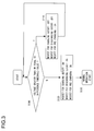
- Fig. 1 is a schematic block diagram showing a power supply device according to the first preferred embodiment of the present invention when it is being used for driving a rotating electrical machine.
- a power supply device 2 is connected to an inverter device 4 via relays 5a and 5b.
- a rotating electrical machine 3 is driven by the inverter device 4 so that it rotates.
- the rotating electrical machine 3 may be a starter motor of an engine idling stop system for starting an engine, or may be a motor generator.
- the power supply device 2 includes a secondary battery 1 such as a lead acid storage battery or the like and a capacitor 10 connected in parallel therewith, a MOSFET for charging cutoff 31, a MOSFET for discharging cutoff 32, a MOSFET for pre-charging 33, a gate driver 12, a control unit 14, a voltage detection unit 16, a temperature detection unit 18, and a current detection unit 20.
- a secondary battery 1 such as a lead acid storage battery or the like and a capacitor 10 connected in parallel therewith
- a MOSFET for charging cutoff 31 a MOSFET for discharging cutoff 32
- MOSFET for pre-charging 33 a MOSFET for pre-charging 33
- a gate driver 12 a control unit 14
- a voltage detection unit 16 a temperature detection unit 18, and a current detection unit 20.
- the capacitor 10 includes a plurality of cells. While, in this embodiment, a low resistance structure is provided by using an N channel MOSFET for each of the MOSFETs 31 through 33, of course it would be possible to use P channel MOSFETs for any one of the MOSFETs or for all of them; any element that can implement a similar function may be applied.
- a voltage boost type gate driver is used for the gate driver 12 that drives the gates of these MOSFETs.
- Any type of voltage boost type gate driver will serve, such as a charge pump type or the like, provided that it is capable of driving the gates of N channel MOSFETs.
- the control unit 14 is a unit that performs overall control of the power supply device as a whole, and, while a dedicated IC or a general purpose microcomputer may be used, these are not limitative; any device that implements similar functions will be acceptable. Apart from its control function for controlling the gate driver 12, the control unit 14 is also endowed with a function of monitoring voltages in various sections, a balance switch function of adjusting the voltage of each cell of the capacitor 10, a function of communicating with a higher level device, and so on.
- the various voltages monitored by the control unit 14 are the total voltage of the secondary battery 1, the voltage of each cell of the capacitor 10 as detected by the voltage detection unit 16 and its total voltage, the output of the current detection unit 20, the output of the temperature detection unit 18, and so on.
- the outputs from each of these sections are inputted and are A/D converted by an A/D converter provided to the control unit 14.
- any required system may be provided for implementing the function of communication with a higher level, such as a CAN (Controller Area Network), an I2C (Inter Integrated Circuit), an SPI (System Packet Interface), or the like.
- a start signal when the rotating electrical machine 3 is to be started is inputted from a higher level via this communication function.
- the device that is used for performing detection of the current is a Hall element
- it would also be acceptable to detect the current by detecting the voltage between both ends across the MOSFET for discharging cutoff 32 and the MOSFET for charging cutoff 31 with a differential amplifier, by measuring the voltage across a shunt resistor, or by measuring the voltage of a current transformer or the like.
- the detected current value is acquired by an A/D converter that is housed within the control unit 14, any arrangement would be acceptable, provided that it can implement a similar function.
- the temperature detection unit 18 detection by dividing a voltage by an NTC thermistor or a PTC thermistor and a resistor in series therewith, or detection by a temperature IC or the like, may be considered, any device would be acceptable, provided that it can implement similar functionality. While, as the subjects for temperature detection, the cells of the capacitor, the board upon which the MOSFETs are mounted, or the chassis may be considered, other elements may be added according to requirements. It should be understood that the temperature detection unit 18 of Fig. 1 is one that detects the temperature of the board upon which the MOSFETs are mounted. While it is supposed that the detected value of temperature is acquired by an A/D converter that is housed within the control unit 14, any device would be acceptable, provided that it can implement similar functionality.
- the MOSFET for discharging cutoff 32 and the MOSFET for charging cutoff 31 are provided in series with the capacitor 10 on a positive side supply path from the capacitor 10 to the secondary battery 1.
- the MOSFET for pre-charging 33 is connected in parallel with the MOSFET for charging cutoff 31. It should be understood that, according to requirements, it would be acceptable to shift the MOSFET for discharging cutoff 32, or the MOSFET for charging cutoff 31 with the MOSFET for pre-charging 33 to the ground side, and it would also be acceptable further to add one or more MOSFETs to the positive side or to the ground side.
- the MOSFET for discharging cutoff 32 is set up so that the forward direction of its body diode 321 is oriented oppositely to the discharge current direction of the capacitor 10.
- the MOSFET for charging cutoff 31 and the MOSFET for pre-charging 33 are set up so that the forward directions of their body diodes 311 and 333 are oriented oppositely to the charging current direction of the capacitor 10.
- the MOSFET for charging cutoff 31 Since the MOSFET for charging cutoff 31 has the body diode 311 that is connected in the opposite direction thereto, accordingly, even if the MOSFET for charging cutoff 31 is turned OFF, still the discharge current from the capacitor 10 is able to flow through the body diode 311 in the forward direction, so that the discharge current is not intercepted.
- the MOSFET for discharging cutoff 32 is provided in series as a switch for interception of the discharge current. When this MOSFET for discharging cutoff 32 is turned OFF, the discharge current is intercepted.
- the MOSFET for charging cutoff 31 is disposed in the power supply line side (i.e. in the positive side), while the MOSFET for discharging cutoff 32 is disposed on the side of the capacitor 1, an opposite arrangement would be equally acceptable.
- the MOSFET for charging cutoff 31, the MOSFET for discharging cutoff 32, and the MOSFET for pre-charging 33 are all put into their ON states. Since a large current flows in the rotating electrical machine 3 at the time of IGN start, accordingly MOSFETs that can handle high current are used for the MOSFET for charging cutoff 31 and for the MOSFET for discharging cutoff 32.
- Fig. 2 is a figure showing the charging current path during pre-charging.
- Fig. 2 the capacitor 10, the secondary battery 1, and the MOSFETs 31 through 33 that are required for explanation of this control method are shown.
- Fig. 3 is a flow chart showing a control procedure for a control program that is executed by the control unit 14.
- step S100 the control unit 14 compares together the total voltage of the secondary battery 1 and the total voltage of the capacitor 10, and makes a decision as to whether or not the potential difference between them is greater than or equal to a threshold potential difference value that has been set in advance. In other words, it makes a decision as to whether or not the voltage of the capacitor 10 is lower than the voltage of the secondary battery 1, and accordingly pre-charging is necessary. While the forward voltage (for example 0.5 V) of the body diode 321 of the MOSFET for discharging cutoff 32 may be considered for this threshold potential difference value, this is not necessarily limitative.
- step S100 If in the step S100 it is determined that the potential difference between the secondary battery 1 and the capacitor 10 is smaller than the threshold potential difference value, then the flow of control proceeds to a step S120, in which each of the MOSFETs 31 through 33 is set to the ON state, in other words the system is put into its normal usage state in which charging and discharging of the capacitor 1 can be performed freely. Thereafter the flow of control proceeds to a step S 130, in which normal operation as a power supply device is started.
- step S 115 in which processing is executed for the pre-charge operation.
- the control unit 14 commands the gate driver 12 to put the MOSFET for charging cutoff 31 and the MOSFET for discharging cutoff 32 into their OFF states, while putting the MOSFET for pre-charging 33 into the ON state. At this time, charging current flows to the capacitor 10 by the path shown by the broken line.
- the charging current In the MOSFET for discharging cutoff 32 that is in the OFF state, the charging current only passes through its body diode 321. On the other hand, the charging current is not able to pass through the MOSFET for charging cutoff 31 that is in the OFF state, so that it flows into the capacitor 10 via the MOSFET for pre-charging 33 that is in the ON state. Charging of the capacitor 10 is performed in this manner. It should be understood that, while the MOSFET for pre-charging 33 is controlled with the normally required gate voltage so as to be kept in the ON state, it would also be acceptable to arrange to adjust the charging current to a more optimum value by adjusting the gate voltage and thereby adjusting the ON resistance of the MOSFET for pre-charging 33.
- the gate voltage may be lowered so as to reduce the value of the charging current.
- PWM Pulse Width Modulation
- the magnitudes of the losses W(32), W(33), and W(10) in the MOSFETs 32 and 33 and the capacitor 10 when a large current flows during pre-charging are related to one another by W(32) > W(33) ⁇ (10), and it is a merit of this structure that the loss is shared with the MOSFET for discharging cutoff 32 that is fundamentally designed for high current and that thus has excellent heat dissipation performance.
- the MOSFET for charging cutoff 31 and the MOSFET for discharging cutoff 32 are provided so as to be connected in series with the capacitor 10, and the MOSFET for pre-charging 33 is provided so as to be connected in parallel with the MOSFET for charging cutoff 31, so that it is arranged, when the voltage of the capacitor 10 is lower than the voltage of the secondary battery 1, to apportion the loss during current limitation between the MOSFET for pre-charging 33 and the MOSFET for discharging cutoff 32.
- MOSFETs 31 and 32 are elements that serve the function of switching circuits that perform opening and closing of the electrical power path for the capacitor 10, and this MOSFET 32 also functions as an element that shares the loss, due to current during pre-charge flowing only to the body diode 321 of this MOSFET 32.
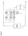
- Fig. 5 is a figure for explanation of a power supply device according to a second embodiment of the present invention, and corresponds to Fig. 2 for the first embodiment. It should be understood that the other structures are the same as in the case of the first embodiment, and accordingly explanation thereof is omitted.
- the MOSFET for discharging cutoff 32 and the MOSFET for charging cutoff 31 are provided in series with the capacitor 10 in the positive side supply path from the capacitor 10 to the secondary battery 1, as shown in Fig. 5 .
- both of the MOSFETS 31 and 32 are in the ON state.
- the gate of the MOSFET for charging cutoff 31 is controlled by PWM control.
- the charging current flows to the capacitor 10 via the body diode 321 of the MOSFET for discharging cutoff 32 and the MOSFET for charging cutoff 31.
- the PWM control for the MOSFET for charging cutoff 31 is adjusted according to the potential difference between the secondary battery 1 and the capacitor 10.
- the magnitudes of the losses W(31), W(32), and W(10) in the MOSFETs 31 and 32 and the capacitor 10 when a large current flows during pre-charging are related to one another by W(32) ⁇ W(31) > W(10), and it is a merit of this structure as well that the loss is dispersed to the MOSFET for discharging cutoff 32 and the MOSFET for charging cutoff 31 that are fundamentally designed for high current and that thus have excellent heat dispersion performance.
- the MOSFET for charging cutoff 31 and the MOSFET for discharging cutoff 32 constitute a switching circuit that is provided so as to be connected in series with the capacitor 10, so that it is arranged, when the voltage of the capacitor 10 is lower than the voltage of the secondary battery 1, to apportion the loss during current limitation between the MOSFET for charging cutoff 31 and the MOSFET for discharging cutoff 32.
- Fig. 6 is a figure for explanation of a power supply device according to a third embodiment of the present invention, and corresponds to Fig. 2 for the first embodiment. While MOSFETs were used as the semiconductor switching elements in the first embodiment described above, in this third embodiment a high voltage capacitor module is used as the capacitor 10, and it is arranged to use IGBT (Insulated Gate Bipolar Transistor) modules instead of MOSFETs.
- IGBT Insulated Gate Bipolar Transistor
- an IGBT for discharging cutoff 42 and an IGBT for charging cutoff 41 are provided in the positive side supply path from the capacitor 10 to the secondary battery 1, in series with the capacitor 10.
- an IGBT for pre-charging 43 is connected in parallel with the IGBT for charging cutoff 41.
- the MOSFETs 31 through 33 shown in Fig. 2 are replaced by IGBTs 41 through 43.
- a hybrid capacitor may be used for the high voltage capacitor 10. By applying a hybrid capacitor whose maximum cell voltage is higher than that of an electric double layer capacitor, it becomes possible to reduce the number of cells that are connected in series.
- the IGBT for discharging cutoff 42 is set up so that its body diode is oriented oppositely to the discharge current direction of the capacitor 10.
- the IGBT for charging cutoff 41 and the IGBT for pre-charging 43 are set up so that their body diodes are oriented oppositely to the charging current direction of the capacitor 10. It should be understood that it would also be acceptable to employ a relay for pre-charging instead of the IGBT for pre-charging 43, since in this embodiment the voltage is high.
- the IGBT for charging cutoff 41, the IGBT for discharging cutoff 42, and the IGBT for pre-charging 43 are all put into their ON states.
- a start signal IGN is inputted from a higher level
- the total voltage of the capacitor 10 and the voltage of the secondary battery 1 are compared together, and, if the voltage of the capacitor 10 is lower than the voltage of the secondary battery 1, then pre-charging is performed.
- the threshold potential difference value that is the decision reference at this time is set to the forward voltage (for example 0.5 V) of the body diode of the IGBT for discharging cutoff 42 or greater, this may be varied according to requirements.
- the current charging path to the capacitor 10 during pre-charging is as shown in Fig. 6 by the broken line, and, after the charging current has passed through the body diode of the IGBT for discharging cutoff 42, it passes through the IGBT for pre-charging 43 and flows into the capacitor 10.
- pseudo increase of the internal resistance can be caused by controlling the current stepwise. Accordingly, by driving the IGBT for pre-charging 43 stepwise, it is possible to increase its proportion of the loss imposed upon the capacitor 10 by pseudo increasing its internal resistance. As a result, even if the potential difference between the secondary battery 1 and the capacitor 10 is large, it is still possible to handle this situation appropriately.
- the gate voltage that is normally required is applied to the IGBT for pre-charging 43 stepwise, it would also be acceptable to arrange to adjust the ON resistance of the IGBT for pre-charging 43 by adjusting its gate voltage, or to adjust the pre-charge current according to PWM control by supplying PWM pulses to the gate of the IGBT for pre-charging 43.
- this embodiment it is arranged to apportion the loss between the IGBT for discharging cutoff 42 that is adapted for high current discharge, the IGBT for pre-charging 43, and the internal resistance of the capacitor 10 , and so it is possible to enhance the heat dissipation performance.
- the magnitudes of the losses W(10), W(42), and W(43) in the capacitor 10 (that is a hybrid capacitor) and the IGBTs 42 and 43 when a large current flows during pre-charging are related to one another by W(10) > W(42) > W(43), and it is a merit of this structure that the loss is dispersed to the IGBT for discharging cutoff 42 that is fundamentally designed for high current and that accordingly has excellent heat dispersion performance.
- it is possible to flow a high current during pre-charging accordingly it is possible to reach a state in which the capacitor 10 can be used over a short time period.
- a semiconductor switching element is used instead of a relay or a limiting resistor as was used in the prior art, accordingly it is possible to anticipate that the system may be made more compact, and that its cost may be reduced.
Landscapes
- Engineering & Computer Science (AREA)
- Power Engineering (AREA)
- Charge And Discharge Circuits For Batteries Or The Like (AREA)
- Electric Propulsion And Braking For Vehicles (AREA)
- Inverter Devices (AREA)
- Dc-Dc Converters (AREA)
Applications Claiming Priority (2)
| Application Number | Priority Date | Filing Date | Title |
|---|---|---|---|
| JP2009034019A JP5200986B2 (ja) | 2009-02-17 | 2009-02-17 | 電源装置 |
| PCT/JP2010/052338 WO2010095641A1 (ja) | 2009-02-17 | 2010-02-17 | 電源装置 |
Publications (1)
| Publication Number | Publication Date |
|---|---|
| EP2400649A1 true EP2400649A1 (de) | 2011-12-28 |
Family
ID=42633921
Family Applications (1)
| Application Number | Title | Priority Date | Filing Date |
|---|---|---|---|
| EP10743767A Withdrawn EP2400649A1 (de) | 2009-02-17 | 2010-02-17 | Stromversorgungsvorrichtung |
Country Status (6)
| Country | Link |
|---|---|
| US (1) | US8803486B2 (de) |
| EP (1) | EP2400649A1 (de) |
| JP (1) | JP5200986B2 (de) |
| KR (1) | KR101273820B1 (de) |
| CN (1) | CN102318176B (de) |
| WO (1) | WO2010095641A1 (de) |
Cited By (10)
| Publication number | Priority date | Publication date | Assignee | Title |
|---|---|---|---|---|
| FR2984623A1 (fr) * | 2011-12-19 | 2013-06-21 | Valeo Equip Electr Moteur | Dispositif de connexion/deconnexion de charge pour unite de stockage d'energie dans un vehicule automobile |
| EP2731229A1 (de) | 2012-11-12 | 2014-05-14 | Saft | Vorladesystem einer Ladekapazität mithilfe einer Batterie |
| CN106463955A (zh) * | 2014-04-29 | 2017-02-22 | 三菱电机株式会社 | 电源开关装置及使用该电源开关装置的系统 |
| EP2337180A3 (de) * | 2009-12-15 | 2017-10-04 | Giesecke+Devrient Mobile Security GmbH | Vorrichtung zum Erzeugen einer gestützten Gleichspannung |
| WO2018087667A1 (de) * | 2016-11-09 | 2018-05-17 | Amrein, Daniel | Kombiniertes stromspeicher-system und management-system hierfür |
| EP3425766A1 (de) * | 2017-07-03 | 2019-01-09 | Ningbo Geely Automobile Research & Development Co. Ltd. | Kondensatormodul |
| EP3633811A1 (de) * | 2018-10-02 | 2020-04-08 | Siemens Aktiengesellschaft | Schutzschaltung |
| EP2639949B1 (de) * | 2012-03-13 | 2020-04-29 | Siemens Aktiengesellschaft | Stromversorgung mit Zwischenkreis |
| EP3654507A1 (de) * | 2018-11-16 | 2020-05-20 | Siemens Aktiengesellschaft | Überwachbares elektrisches bauelement mit mindestens einer funktionalen ausrichtung als kondensator |
| US20230170713A1 (en) * | 2020-04-10 | 2023-06-01 | Sony Group Corporation | Control apparatus and control method |
Families Citing this family (45)
| Publication number | Priority date | Publication date | Assignee | Title |
|---|---|---|---|---|
| DE102004005576B4 (de) * | 2003-02-25 | 2021-03-11 | Heidelberger Druckmaschinen Ag | Verfahren zum Betrieb einer Lackier- oder Druckmaschine |
| DE102010039875A1 (de) * | 2010-08-27 | 2012-03-01 | Robert Bosch Gmbh | Verfahren und Vorrichtung zum Betreiben eines Starters eines Fahrzeugs |
| US9166515B2 (en) * | 2010-12-20 | 2015-10-20 | Toyota Jidosha Kabushiki Kaisha | Electrically powered vehicle and method for controlling the same |
| US9073438B2 (en) * | 2011-10-28 | 2015-07-07 | General Electric Company | System for selectively coupling an energy source to a load and method of making same |
| US8674757B2 (en) * | 2011-11-01 | 2014-03-18 | Neoenergy Microelectronic, Inc. | Switching system and method for control thereof |
| JP2014079078A (ja) * | 2012-10-10 | 2014-05-01 | Fuji Electric Co Ltd | 電動機駆動システム |
| FR3000626B1 (fr) | 2013-01-02 | 2015-02-27 | Renault Sa | Systeme comprenant une batterie formee de modules de batterie, et procede de connexion ou de deconnexion d'un module de batterie correspondant |
| WO2015000017A1 (en) * | 2013-06-28 | 2015-01-08 | Cap-Xx Limited | A current limit circuit for a supercapacitive device |
| US9931947B2 (en) * | 2013-08-30 | 2018-04-03 | Infineon Technologies Ag | Charging a capacitor |
| US9925878B2 (en) | 2013-09-26 | 2018-03-27 | Ford Global Technologies, Llc | Bus pre-charge control using a buck converter |
| US9214888B2 (en) * | 2013-12-20 | 2015-12-15 | Lg Chem, Ltd. | Pre-charging system for a capacitor in a voltage inverter for an electric motor |
| KR101551035B1 (ko) * | 2013-12-30 | 2015-09-08 | 현대자동차주식회사 | 프리 차지 중 고장 진단 방법 |
| US9630503B2 (en) * | 2014-02-06 | 2017-04-25 | Ford Global Technologies, Llc | Energizing an automotive vehicle high voltage bus using a single main contactor |
| US9573474B2 (en) * | 2014-03-06 | 2017-02-21 | Ford Global Technologies, Llc | Capacitor precharging and capacitance/resistance measurement in electric vehicle drive system |
| JP6123764B2 (ja) * | 2014-09-11 | 2017-05-10 | トヨタ自動車株式会社 | 電源システム |
| JP6322123B2 (ja) * | 2014-11-04 | 2018-05-09 | 矢崎総業株式会社 | 電流制限回路 |
| US10074620B2 (en) | 2015-03-25 | 2018-09-11 | Infineon Technologies Americas Corp. | Semiconductor package with integrated output inductor using conductive clips |
| KR102442187B1 (ko) * | 2015-04-10 | 2022-09-07 | 삼성에스디아이 주식회사 | 배터리 보호 회로 |
| US10199843B2 (en) | 2015-05-26 | 2019-02-05 | Infineon Technologies Americas Corp. | Connect/disconnect module for use with a battery pack |
| JP2017022872A (ja) * | 2015-07-10 | 2017-01-26 | トヨタ自動車株式会社 | 電源システム |
| KR102406818B1 (ko) | 2015-09-02 | 2022-06-10 | 삼성전자주식회사 | 전력 회로 |
| US9923470B2 (en) | 2015-09-18 | 2018-03-20 | Lear Corporation | High voltage pre-charge system |
| US10181724B2 (en) * | 2016-02-10 | 2019-01-15 | Eguana Technologies | Seamless transitions between control modes |
| US10305321B2 (en) | 2016-02-10 | 2019-05-28 | Eguana Technologies | Automatic recovery control |
| US11139654B2 (en) | 2016-02-10 | 2021-10-05 | Eguana Technologies | Output control and compensation for AC coupled systems |
| DE102016219098A1 (de) | 2016-09-30 | 2018-04-05 | Volkswagen Aktiengesellschaft | Batterie-Trenneinrichtung |
| DE102016220118B4 (de) * | 2016-10-14 | 2022-01-05 | Volkswagen Aktiengesellschaft | Batterie-Trenneinrichtung und Verfahren zur Durchführung eines Vorladezyklus |
| JP6867780B2 (ja) * | 2016-10-28 | 2021-05-12 | 矢崎総業株式会社 | 半導体スイッチ制御装置 |
| JP6545230B2 (ja) * | 2017-08-31 | 2019-07-17 | 本田技研工業株式会社 | 車両の電源システム |
| KR102056876B1 (ko) * | 2017-09-25 | 2019-12-17 | 주식회사 엘지화학 | 배터리 관리 장치와 이를 포함하는 배터리 팩 및 자동차 |
| KR102204983B1 (ko) | 2017-09-25 | 2021-01-18 | 주식회사 엘지화학 | 배터리 관리 장치와 이를 포함하는 배터리 팩 및 자동차 |
| JP6879170B2 (ja) * | 2017-11-08 | 2021-06-02 | トヨタ自動車株式会社 | 車両用電源システム |
| JP6885302B2 (ja) * | 2017-11-08 | 2021-06-09 | トヨタ自動車株式会社 | 車両用電源システム |
| CN107959324B (zh) * | 2017-11-21 | 2020-11-24 | 上海空间电源研究所 | 航天器电源系统储能电池放电开关电路 |
| JP6732831B2 (ja) * | 2018-04-10 | 2020-07-29 | 矢崎総業株式会社 | 電源供給装置 |
| US11196133B2 (en) * | 2018-10-30 | 2021-12-07 | Cps Technology Holdings Llc | Solid-state relay dedicated recirculation path systems and methods |
| CN110962630B (zh) * | 2018-12-04 | 2021-06-25 | 宁德时代新能源科技股份有限公司 | 预充电流的调控方法和电路 |
| CN110239372B (zh) * | 2019-06-10 | 2021-10-22 | 上海师范大学 | 一种bms预充电路及其控制方法 |
| CN110277814B (zh) * | 2019-06-18 | 2023-06-13 | Oppo广东移动通信有限公司 | 待充电设备及充电方法 |
| CN110176857B (zh) * | 2019-06-20 | 2024-04-09 | 中国重型机械研究院股份公司 | 一种整流单元预充电回路增容电路及其搭建方法 |
| KR20210047142A (ko) * | 2019-10-21 | 2021-04-29 | 주식회사 엘지화학 | 프리차지 회로 및 이를 포함하는 배터리 시스템 |
| US11726130B2 (en) * | 2020-08-26 | 2023-08-15 | Eaton Intelligent Power Limited | Hybrid switch for substation and other applications and methods of operating same |
| CN114079419B (zh) * | 2021-11-10 | 2023-09-19 | 大庆正方软件科技股份有限公司 | 基于群电容控制泵升电压的系统 |
| GB2618525A (en) * | 2022-05-03 | 2023-11-15 | Siemens Energy AS | Energy storage system |
| US11955974B2 (en) * | 2022-06-30 | 2024-04-09 | Infineon Technologies Ag | Dual gate MOSFET devices and pre-charging techniques for DC link capacitors |
Family Cites Families (21)
| Publication number | Priority date | Publication date | Assignee | Title |
|---|---|---|---|---|
| JPH07115728A (ja) * | 1992-08-28 | 1995-05-02 | Tai-Her Yang | 複数の独立直流電源による多段階複電圧出力回路 |
| JP3330050B2 (ja) * | 1997-03-11 | 2002-09-30 | 本田技研工業株式会社 | 電気自動車の制御装置 |
| JP3799398B2 (ja) * | 1999-10-28 | 2006-07-19 | 富士電機デバイステクノロジー株式会社 | 半導体電力変換システム |
| US6798175B2 (en) * | 2000-04-11 | 2004-09-28 | Pentax Corporation | Power supply circuit |
| JP2005269873A (ja) * | 2004-03-22 | 2005-09-29 | Toyota Industries Corp | 高周波電流用配線部材とその製造方法および電力変換装置 |
| JP2005312156A (ja) | 2004-04-20 | 2005-11-04 | Toyota Motor Corp | 電源制御装置およびそれを備えたモータ駆動装置 |
| EP1762124B1 (de) * | 2004-05-06 | 2017-09-06 | Continuum Electro-Optics, Inc. | Verfahren und vorrichtungen für einen verbesserten verstärker zur ansteuerung einer nichtlinearen last |
| JP4162645B2 (ja) * | 2004-10-05 | 2008-10-08 | 三洋電機株式会社 | 車両用の電源装置 |
| JP4547231B2 (ja) * | 2004-10-22 | 2010-09-22 | 日立オートモティブシステムズ株式会社 | 電力変換装置 |
| US7573238B2 (en) * | 2005-08-09 | 2009-08-11 | Panasonic Ev Energy Co., Ltd. | Voltage detection device and electric vehicle including voltage detection device |
| WO2007026492A1 (ja) * | 2005-08-30 | 2007-03-08 | Fuji Jukogyo Kabushiki Kaisha | リチウムイオンキャパシタ |
| JP4542483B2 (ja) * | 2005-08-31 | 2010-09-15 | 日立コンピュータ機器株式会社 | スイッチング電源装置及びディスクアレイシステム |
| JP4910369B2 (ja) | 2005-11-15 | 2012-04-04 | トヨタ自動車株式会社 | 電源制御装置 |
| JP2007191088A (ja) | 2006-01-20 | 2007-08-02 | Nissan Diesel Motor Co Ltd | ハイブリッド車両 |
| JP2007244124A (ja) * | 2006-03-09 | 2007-09-20 | Toyota Motor Corp | 車両駆動用電源システム |
| KR100839740B1 (ko) | 2006-11-06 | 2008-06-19 | 삼성에스디아이 주식회사 | 하이브리드 배터리 및 그것의 충전 방법 |
| JP4810417B2 (ja) * | 2006-12-20 | 2011-11-09 | 富士重工業株式会社 | 蓄電デバイスの残存容量演算装置 |
| KR101089833B1 (ko) | 2007-01-11 | 2011-12-05 | 주식회사 엘지화학 | 전지 보호용 소프트 스타트 회로 및 이를 구비하는 전지팩 |
| CN101340147B (zh) | 2007-07-05 | 2011-03-23 | 立锜科技股份有限公司 | 在预充电模式抑制电压转换器输入电流突增的装置及方法 |
| JP4758959B2 (ja) | 2007-07-31 | 2011-08-31 | キユーピー株式会社 | 半割り茹卵様卵加工品及びその製造方法 |
| US7656061B2 (en) * | 2007-10-29 | 2010-02-02 | Bose Corporation | Automatic power source configuration |
-
2009
- 2009-02-17 JP JP2009034019A patent/JP5200986B2/ja not_active Expired - Fee Related
-
2010
- 2010-02-17 WO PCT/JP2010/052338 patent/WO2010095641A1/ja active Application Filing
- 2010-02-17 CN CN201080008214.3A patent/CN102318176B/zh not_active Expired - Fee Related
- 2010-02-17 US US13/145,432 patent/US8803486B2/en not_active Expired - Fee Related
- 2010-02-17 KR KR1020117018996A patent/KR101273820B1/ko not_active IP Right Cessation
- 2010-02-17 EP EP10743767A patent/EP2400649A1/de not_active Withdrawn
Non-Patent Citations (1)
| Title |
|---|
| See references of WO2010095641A1 * |
Cited By (21)
| Publication number | Priority date | Publication date | Assignee | Title |
|---|---|---|---|---|
| EP2337180A3 (de) * | 2009-12-15 | 2017-10-04 | Giesecke+Devrient Mobile Security GmbH | Vorrichtung zum Erzeugen einer gestützten Gleichspannung |
| FR2984623A1 (fr) * | 2011-12-19 | 2013-06-21 | Valeo Equip Electr Moteur | Dispositif de connexion/deconnexion de charge pour unite de stockage d'energie dans un vehicule automobile |
| WO2013093273A1 (fr) * | 2011-12-19 | 2013-06-27 | Valeo Equipements Electriques Moteur | Dispositif de connexion/deconnexion de charge pour unite de stockage d'energie dans un vehicule automobile |
| EP2639949B1 (de) * | 2012-03-13 | 2020-04-29 | Siemens Aktiengesellschaft | Stromversorgung mit Zwischenkreis |
| EP2731229A1 (de) | 2012-11-12 | 2014-05-14 | Saft | Vorladesystem einer Ladekapazität mithilfe einer Batterie |
| CN106463955A (zh) * | 2014-04-29 | 2017-02-22 | 三菱电机株式会社 | 电源开关装置及使用该电源开关装置的系统 |
| EP3125391A4 (de) * | 2014-04-29 | 2017-10-18 | Mitsubishi Electric Corporation | Leistungsschaltervorrichtung und system damit |
| US9935480B2 (en) | 2014-04-29 | 2018-04-03 | Mitsubishi Electric Corporation | Power switch device and system using same |
| CN106463955B (zh) * | 2014-04-29 | 2020-01-21 | 三菱电机株式会社 | 电源开关装置及使用该电源开关装置的系统 |
| WO2018087667A1 (de) * | 2016-11-09 | 2018-05-17 | Amrein, Daniel | Kombiniertes stromspeicher-system und management-system hierfür |
| CN110832190A (zh) * | 2017-07-03 | 2020-02-21 | 宁波吉利汽车研究开发有限公司 | 一种电容器模块 |
| EP3425766A1 (de) * | 2017-07-03 | 2019-01-09 | Ningbo Geely Automobile Research & Development Co. Ltd. | Kondensatormodul |
| US11146097B2 (en) | 2017-07-03 | 2021-10-12 | Ningbo Geely Automobile Research & Development Co. | Capacitor module |
| EP3633811A1 (de) * | 2018-10-02 | 2020-04-08 | Siemens Aktiengesellschaft | Schutzschaltung |
| WO2020069894A1 (en) * | 2018-10-02 | 2020-04-09 | Siemens Aktiengesellschaft | Protection circuit |
| CN112789777A (zh) * | 2018-10-02 | 2021-05-11 | 西门子股份公司 | 保护电路 |
| US11764566B2 (en) | 2018-10-02 | 2023-09-19 | Siemens Aktiengesellschaft | Protection circuit |
| CN112789777B (zh) * | 2018-10-02 | 2024-02-20 | 西门子股份公司 | 保护电路 |
| EP3654507A1 (de) * | 2018-11-16 | 2020-05-20 | Siemens Aktiengesellschaft | Überwachbares elektrisches bauelement mit mindestens einer funktionalen ausrichtung als kondensator |
| US20230170713A1 (en) * | 2020-04-10 | 2023-06-01 | Sony Group Corporation | Control apparatus and control method |
| EP4135141A4 (de) * | 2020-04-10 | 2023-09-20 | Sony Group Corporation | Steuerungsvorrichtung und steuerungsverfahren |
Also Published As
| Publication number | Publication date |
|---|---|
| KR20110105001A (ko) | 2011-09-23 |
| JP5200986B2 (ja) | 2013-06-05 |
| US20110316489A1 (en) | 2011-12-29 |
| WO2010095641A1 (ja) | 2010-08-26 |
| KR101273820B1 (ko) | 2013-06-11 |
| CN102318176A (zh) | 2012-01-11 |
| JP2010193588A (ja) | 2010-09-02 |
| US8803486B2 (en) | 2014-08-12 |
| CN102318176B (zh) | 2015-05-13 |
Similar Documents
| Publication | Publication Date | Title |
|---|---|---|
| US8803486B2 (en) | Power supply device | |
| JP5440400B2 (ja) | 電源装置 | |
| EP2272722B1 (de) | Stromquellenvorrichtung für ein Fahrzeug | |
| US9431850B2 (en) | Power supply unit having plurality of secondary batteries | |
| US6995480B2 (en) | Power supply equipment for motor vehicle with inverter for controlling motor generator | |
| CN102377215B (zh) | 用于推进蓄电池的组合加热及预充电功能和硬件 | |
| US9520613B2 (en) | Battery control with block selection | |
| US9855904B2 (en) | Coupling store device for a motor vehicle | |
| US8760111B2 (en) | Secondary battery output power controller | |
| JP2014183705A (ja) | 2電源負荷駆動システム及び燃料電池自動車 | |
| CN113954686A (zh) | 一种电池包、电池管理系统及车辆 | |
| JP2006060883A (ja) | 2バッテリ型車両用電源装置 | |
| JP2005269828A (ja) | ハイブリッドシステム | |
| US11702060B2 (en) | Power relay assembly and vehicle comprising the same and control method of power relay assembly | |
| CN111016731B (zh) | 一种充电保护电路、电动汽车的充电方法及电动汽车 | |
| EP3560060B1 (de) | Hochleistungs-flashbatteriesystem und verfahren dafür | |
| JP6430100B2 (ja) | ショベル | |
| CN215883385U (zh) | 一种电池包、电池管理系统及车辆 | |
| CN115986863A (zh) | 能量储存设备、能量储存系统、控制方法和预充电电路 | |
| CN114448000A (zh) | 防护电路及其方法 | |
| JP2005269826A (ja) | ハイブリッドシステムの充電制御回路 |
Legal Events
| Date | Code | Title | Description |
|---|---|---|---|
| PUAI | Public reference made under article 153(3) epc to a published international application that has entered the european phase |
Free format text: ORIGINAL CODE: 0009012 |
|
| 17P | Request for examination filed |
Effective date: 20110919 |
|
| AK | Designated contracting states |
Kind code of ref document: A1 Designated state(s): AT BE BG CH CY CZ DE DK EE ES FI FR GB GR HR HU IE IS IT LI LT LU LV MC MK MT NL NO PL PT RO SE SI SK SM TR |
|
| DAX | Request for extension of the european patent (deleted) | ||
| STAA | Information on the status of an ep patent application or granted ep patent |
Free format text: STATUS: THE APPLICATION IS DEEMED TO BE WITHDRAWN |
|
| 18D | Application deemed to be withdrawn |
Effective date: 20160901 |