EP2390908A2 - Verfahren zur Herstellung einer Verpackung einer elektronischen Vorrichtung - Google Patents
Verfahren zur Herstellung einer Verpackung einer elektronischen Vorrichtung Download PDFInfo
- Publication number
- EP2390908A2 EP2390908A2 EP11159482A EP11159482A EP2390908A2 EP 2390908 A2 EP2390908 A2 EP 2390908A2 EP 11159482 A EP11159482 A EP 11159482A EP 11159482 A EP11159482 A EP 11159482A EP 2390908 A2 EP2390908 A2 EP 2390908A2
- Authority
- EP
- European Patent Office
- Prior art keywords
- substrate
- cover substrate
- base substrate
- metal film
- cover
- Prior art date
- Legal status (The legal status is an assumption and is not a legal conclusion. Google has not performed a legal analysis and makes no representation as to the accuracy of the status listed.)
- Withdrawn
Links
Images

Classifications
-
- H10W76/13—
-
- H10W76/60—
-
- H—ELECTRICITY
- H03—ELECTRONIC CIRCUITRY
- H03H—IMPEDANCE NETWORKS, e.g. RESONANT CIRCUITS; RESONATORS
- H03H9/00—Networks comprising electromechanical or electro-acoustic elements; Electromechanical resonators
- H03H9/02—Details
- H03H9/05—Holders or supports
- H03H9/10—Mounting in enclosures
- H03H9/1007—Mounting in enclosures for bulk acoustic wave [BAW] devices
- H03H9/1014—Mounting in enclosures for bulk acoustic wave [BAW] devices the enclosure being defined by a frame built on a substrate and a cap, the frame having no mechanical contact with the BAW device
-
- H—ELECTRICITY
- H03—ELECTRONIC CIRCUITRY
- H03H—IMPEDANCE NETWORKS, e.g. RESONANT CIRCUITS; RESONATORS
- H03H9/00—Networks comprising electromechanical or electro-acoustic elements; Electromechanical resonators
- H03H9/02—Details
- H03H9/05—Holders or supports
- H03H9/10—Mounting in enclosures
- H03H9/1064—Mounting in enclosures for surface acoustic wave [SAW] devices
- H03H9/1071—Mounting in enclosures for surface acoustic wave [SAW] devices the enclosure being defined by a frame built on a substrate and a cap, the frame having no mechanical contact with the SAW device
-
- H10W95/00—
-
- H10W72/0198—
-
- H10W72/884—
-
- H10W90/734—
-
- H10W90/754—
Definitions
- the present invention relates to a package for a surface mount device (SMD) in which an electronic device is encapsulated in a cavity formed between two substrates bonded together, and more particularly, to a structure to bond two substrates.
- SMD surface mount device
- a manufacturing method of a package in the related art in which a base substrate and a cover substrate are bonded together via a metal film will now be described.
- a description will be given to a manufacturing method by which a plurality of package elements are formed in array on a single sheet of base substrate and after a cover substrate is bonded to the base substrate, the bonded substrates are divided into individual packages.
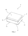
- an electronic device package in the related art includes an electronic device 47, a plate-shaped base substrate 41, a cover substrate 42 provided with a concave portion, and a metal film 49, which is a bonding film to bond the base substrate 41 and the cover substrate 42 together. Because the cover substrate 42 is provided with a concave portion, a cavity 46 is formed by sealing the base substrate 41 with the cover substrate 42. The electronic device 47 is accommodated in the cavity 46.
- the base substrate 41 is formed of an insulator, a semiconductor, or metal and formed in a plate shape.
- Wires 43 used to mount the electronic devices 47 are formed on the surface of the base substrate 41 in a number according to the number of the electronic devices 47 to be mounted.
- Outside electrodes 45 are formed on the back surface of the base substrate 41 in a corresponding manner to the wires 43.
- through-holes are formed at arbitrary portions of the packages and feed-through electrodes 44 are formed to fill the respective through-holes. The wires 43 and the outside electrodes 45 are thus connected via the feed-through electrodes 44.
- the cover substrate 42 is formed of an insulator, a semiconductor, or metal and formed to have concave portions.
- a metal film 49 is formed as the bonding film in a portion where the base substrate 41 and the cover substrate 42 come into contact with each other. Basically, it is sufficient to form the metal film 49 only on the portion where the base substrate 41 and the cover substrate 42 come into contact with each other. However, by taking simplification of the steps into account, as is shown in Fig. 7B , the metal film 49 is formed entirely on one surface of the cover substrate 42.
- a plurality of concave cavities 46 are formed in a wafer of cover substrate 42 so that a plurality of electronic devices 47 can be mounted therein ( Fig. 7A ).
- the metal film 49 as a bonding film is formed on one surface of the cover substrate 42 ( Fig. 7B ).
- Aluminum, chrome, silicon, and copper are suitable as the metal film 49.
- the wires 43 used to mount a plurality of the electronic devices 47 on a wafer of base substrate 41, the outside electrodes 45, and the feed-through electrodes 44 are formed ( Fig. 7C ).
- the electronic devices 47 are mounted on the base substrate 41 and the electronic devices 47 and the wires 43 are connected with wires 48 by wire bonding ( Fig. 7D ).
- the base substrate 41 and the cover substrate 42 are aligned and superimposed, and then bonded together.
- the base substrate 41 and the cover substrate 42 aligned with each other are sandwiched by substrates 50 and 51 serving as heaters and also as electrodes.
- a positive electrode probe 52 is set so as to come into contact with the metal film 49 and temperatures of the substrates 50 and 51 serving as heaters and also as electrodes are raised.
- a voltage is then applied between the positive electrode probe 52 and the substrate 50 serving as a heater and also as an electrode. Consequently, the base substrate 41 and the cover substrate 42 are bonded together via the metal film 49. Thereafter, package elements are cut off individually using a dicing apparatus or the like. Individual electronic device packages are thus completed.
- the manufacturing method of the electronic device package in the related art has problems as follows. Firstly, because a plurality of concave portions that later form the cavities 46 are formed in one surface of the cover substrate 42, when the cover substrate 42 is made thinner, shapes of one surface and the other surface of the cover substrate 42 differ from each other. This poses a problem that the cover substrate 42 warps considerably. To eliminate this problem, a countermeasure to suppress warping is taken by increasing a film thickness of the metal film 49 formed on the cover substrate 42 on the surface in which the concave portions are formed. However, when the metal film 49 becomes thicker, there arises another problem that bonding strength between the metal film 49 and the base substrate 41 becomes lower.
- the invention was devised in view of the foregoing and has an object to provide an electronic device package in which a base substrate and a cover substrate are bonded together via a metal film in a stable manner by minimizing warping of the substrate even when the substrate whose one surface and other surface have different shapes is made thinner.
- a manufacturing method of an electronic device package is a manufacturing method of an electronic device package including a base substrate, a cover substrate bonded to the base substrate while being opposed to the base substrate, and electronic devices respectively accommodated in a plurality of cavities formed between the base substrate and the cover substrate and mounted on the base substrate.
- the manufacturing method includes: forming concave portions that later form the cavities in one surface of the cover substrate; forming a first metal film on the other surface of the cover substrate; forming a second metal film on the one surface of the cover substrate; and bonding the base substrate and the cover substrate together via the second metal film.
- the metal film is also formed on the cover substrate on the surface opposite to the surface in which the concave portions are formed. Accordingly, even when the cover substrate becomes extremely thin, this metal film plays a role of preventing warping of the cover substrate. Hence, there can be achieved an advantage that warping of the cover substrate can be suppressed to the least extent when the base substrate and the cover substrate are bonded together. Further, because the metal film is formed on the cover substrate on the surface opposite to the surface bonded to the base substrate, there can be achieved another advantage that a product identification number can be inscribed on this metal film. In a case where the cover substrate is an insulator, it has been quite difficult to inscribe the product identification number on the cover substrate on the surface opposite to the surface bonded to the base substrate.
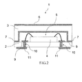
- an electronic device package 1 of this embodiment is a surface mount device package including a base substrate 2 and a cover substrate 3 laminated in two layers in a box shape and an electronic device 4 accommodated in a cavity 5 formed inside the box.
- the electronic device 4 is, for example, an LSI, an MEMS, a sensor, and a piezoelectric transducer, or a complex thereof.
- Both the base substrate 2 and the cover substrate 3 are formed of an insulator, a semiconductor, metal, or a combination thereof and both are an insulator made, for example, of soda glass in this embodiment.
- a rectangular concave portion that later forms a cavity 5 in which to accommodate the electronic deice 4 is formed in the cover substrate 3 on the surface to which the base substrate 2 is bonded and the base substrate 2 is formed in a plate shape.
- the concave portion 5 is a concave portion that later forms the cavity 5 in which to accommodate the electronic device 4 when the both substrates 2 and 3 are superimposed.
- the cover substrate 3 is bonded to the base substrate 2 via a metal film 7, which is a bonding film, in a state where the concave portion 5 is opposed to the base substrate 2.
- feed-through electrodes 10 are formed in the base substrate 2 to electrically connect the electronic device 4 and outside electrodes 11.
- Through-holes in which to insert the feed-through electrodes 10 are formed to open within the cavity 5.
- through-holes may be tapered by gradually increasing or decreasing the diameter toward the bottom surface of the base substrate 2. In any case, it is sufficient that through-holes penetrate through the base substrate 2.
- the feed-through electrodes 10 are formed in the respective through-holes so as to fill the through-holes.
- the feed-through electrodes 10 play not only a role of maintaining the interior of the cavity 5 hermetically by completely closing the through-holes but also a role of bringing the outside electrodes 11 and the electric device 4 into conduction.
- a clearance between the through-hole and the feed-through electrode 10 is completely filled using a material, such as an inorganic material or an organic material, having a thermal expansion coefficient adjusted to that of the base substrate 2.
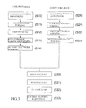
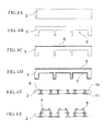
- the base substrate 2 is obtained by polishing and etching a wafer of insulating substrate until it reaches a target thickness followed by rinsing (S10). Subsequently, through-holes are formed in the base substrate 2 (S11).
- the through-holes can be formed by any appropriate method and etching by photolithography and press working are applicable.
- Wires 9 used to mount the electronic devices 4 on the base substrate 2 are formed (S12). Subsequently, the feed-through electrodes 10 are formed in the through-holes formed in the base substrate 2 (S13). Further, the outside electrodes 11 are formed on the base substrate 2 on the surface opposite to the surface on which the wires 9 are formed (S14). Fig. 4E shows the base substrate 2 in a state where the outside electrodes 11 have been formed.
- the cover substrate 3 is obtained by polishing and etching a wafer of insulating substrate until it reaches a target thickness followed by rinsing (S20).
- a target thickness followed by rinsing S20
- concave portions that later form the cavities 5 are formed in the cover substrate 3 of a plate shape (S21).
- the concave portions can be formed by any appropriate method and etching by photolithography and press working are applicable.
- a first metal film 6 to prevent warping of a wafer is formed on the cover substrate 3 on the entire surface opposite to the surface in which the concave portions are formed (S22).
- the first metal film 6 is formed using methods, such as vapor deposition, sputtering, and CVD.
- a material having a smaller linear expansion coefficient than a material used for the cover substrate 3 is used.
- Si, Cr, W, or a combination thereof is used for the first metal film 6, and a thickness thereof is set to a range of 200 angstroms to 2000 angstroms.
- Soda glass has a linear expansion coefficient of 9 to 10 ⁇ 10 -6 /°C whereas Si has a linear expansion coefficient of 2.8 to 7.3 ⁇ 10 -6 /°C, Cr has a linear expansion coefficient of 6.2 ⁇ 10 -6 /°C, and W has a linear expansion coefficient of 4.3 ⁇ 10 -6 /°C .
- a second metal film 7 as a bonding film is formed on the cover substrate 3 on the entire surface in which the concave portions are formed (S23).
- the second metal film 7 is formed using methods, such as vapor deposition, sputtering, and CVD.
- a material having a larger linear expansion coefficient than a material used for the cover substrate 3 is used for the second metal film 7 whenever possible.
- soda glass is used for the cover substrate 3
- Al, Ni, Au-Sn, or Cu is used for the second metal film 7 and a thickness thereof is set to a range of 200 angstroms to 2000 angstroms.
- a material of the second metal film 7 is not necessarily limited to a material having a larger linear expansion coefficient than a material used for the cover substrate 3 and Si, Cr, or W may be used in a case where the cover substrate 3 is made of soda glass.
- Al has a linear expansion coefficient of 23.9 ⁇ 10 -6 /°C
- Ni has a linear expansion coefficient of 13 ⁇ 10 -6 /°C
- Au has a linear expansion coefficient of 14.2 ⁇ 10 -6 /°C
- Sn has a linear expansion coefficient of 23 ⁇ 10 -6 /°C
- Cu has a linear expansion coefficient of 13 ⁇ 10 -6 /°C.
- a priority is placed on a bonding method of the cover substrate 3 and the base substrate 2 when selecting a material of the second metal film 7 formed on the cover substrate 3 on the surface in which the concave portions are formed.
- the second metal film 7 has a smaller linear expansion coefficient than a material used for the cover substrate 3, then warping of the cover substrate 3 as a wafer is reduced by increasing a thickness of the first metal film 6 formed on the cover substrate 3 on the surface opposite to the surface in which the concave portions are formed.
- Fig. 4F shows a case where the wires 9 and the electronic devices 4 are connected by wire bonding using wires 8.
- the invention is not limited to this connection method. As long as electric conduction is ensured, any connection method, such as flip chip bonding and solder bonding, is applicable.
- the film thickness of the metal films 6 and 7 is limited to the range of 200 angstroms to 2000 angstroms because of a relation with stability in film formation and bonding strength.
- adhesion strength between the material of the cover substrate 3 and the metal films 6 and 7 is weak.
- a film thickness of 200 angstroms or more is necessary.
- bonding strength between the base substrate 2 and the cover substrate 3 becomes dependent on an intermolecular bonding force of the film and the bonding strength is lowered.
- the base substrate 2 on which are mounted the electronic devices 4 and the cover substrate 3 on which is formed the first metal film 6 are bonded together via the second metal film 7 (S31).
- the base substrate 2 is formed in an adequate size to be superimposed on the cover substrate 3.
- the bonding method of the base substrate 2 and the cover substrate 3 is selected according to materials forming the respective base substrate 2 and cover substrate 3 and the type of the second metal film 7.
- anodic bonding is suitable as the bonding method.
- Fig. 5A shows a case where the base substrate 2 and the cover substrate 3 are bonded together by anodic bonding.
- the cover substrate 3 and the base substrate 2 are aligned and superimposed first.
- a negative electrode plate 21 made of carbon or the like is brought into contact with the base substrate 2 on the entire surface opposite to the surface bonded to the cover substrate 3.
- a positive electrode plate 22 made of carbon or the like is brought into contact with the cover substrate 3 on the entire surface opposite to the surface bonded to the base substrate 2. Further, a certain load is applied between the positive electrode plate 22 and the negative electrode plate 21. In this state, the positive electrode plate 22, the negative electrode plate 21, the base substrate 2, and the cover substrate 3 are heated to 200 to 300°C by a heater or the like and a voltage of 500 to 1000 V is applied between the positive electrode plate 22 and the negative electrode plate 21. The base substrate 2 and the cover substrate 3 are thus bonded together by anodic bonding.
- a plurality of electronic device package elements are present in a single wafer obtained by bonding a wafer of base substrate 2 and a wafer of cover substrate 3. Accordingly, as is shown in Fig. 5B , the electronic device packages 1 are cut off individually using a dicing saw or a wire saw (S32).
- Fig. 2 shows a cross section of one individually cut-off electronic device package 1. Thereafter, the electronic device package 1 is completed by conducting an inspection on the internal electric property (S33).
- the scope of the invention is not limited to the embodiment described above and various modifications can be made without deviating from the scope of the invention.
- the embodiment above has described a case where both the base substrate 2 and the cover substrate 3 are made of soda glass and the base substrate 2 and the cover substrate 3 are bonded together by anodic bonding.
- the invention is not limited to this case.
- the base substrate 2 and the cover substrate 3 may be bonded together via the metal film 7 by welding or by eutectic bonding.
- an oscillator 100 of this embodiment includes, as a transducer electrically connected to an integrated circuit 101, the electronic device package 1 (piezoelectric transducer) using a piezoelectric vibrating piece made, for example, of quartz, as the electronic device 4.
- the oscillator 100 includes a substrate 103 on which an electronic component 102, such as a capacitor, is mounted.
- the integrated circuit 101 for oscillator is mounted on the substrate 103 and the electronic device package 1 (piezoelectric transducer) is mounted thereon in the vicinity of the integrated circuit 101.
- the electronic component 102, the integrated circuit 101, and the electronic device package 1 (piezoelectric transducer) are electrically interconnected by an unillustrated wiring pattern. Each component is molded with unillustrated resin.
- the piezoelectric vibrating piece in the piezoelectric transducer vibrates.
- the vibration is converted to an electric signal by the piezoelectric characteristic of the piezoelectric vibrating piece and inputted into the integrated circuit 101 as the electric signal.
- the integrated circuit 101 applies various types of processing to the electric signal inputted therein and outputs the resulting signal as a frequency signal.
- the piezoelectric transducer thus functions as an oscillator.
Landscapes
- Physics & Mathematics (AREA)
- Acoustics & Sound (AREA)
- Piezo-Electric Or Mechanical Vibrators, Or Delay Or Filter Circuits (AREA)
- Oscillators With Electromechanical Resonators (AREA)
- Surface Acoustic Wave Elements And Circuit Networks Thereof (AREA)
Applications Claiming Priority (1)
| Application Number | Priority Date | Filing Date | Title |
|---|---|---|---|
| JP2010073340A JP5538974B2 (ja) | 2010-03-26 | 2010-03-26 | 電子デバイスパッケージの製造方法及び電子デバイスパッケージ |
Publications (2)
| Publication Number | Publication Date |
|---|---|
| EP2390908A2 true EP2390908A2 (de) | 2011-11-30 |
| EP2390908A3 EP2390908A3 (de) | 2014-01-01 |
Family
ID=44202509
Family Applications (1)
| Application Number | Title | Priority Date | Filing Date |
|---|---|---|---|
| EP11159482.6A Withdrawn EP2390908A3 (de) | 2010-03-26 | 2011-03-23 | Verfahren zur Herstellung einer Verpackung einer elektronischen Vorrichtung |
Country Status (6)
| Country | Link |
|---|---|
| US (1) | US8530986B2 (de) |
| EP (1) | EP2390908A3 (de) |
| JP (1) | JP5538974B2 (de) |
| KR (1) | KR101872518B1 (de) |
| CN (1) | CN102254836B (de) |
| TW (1) | TWI506737B (de) |
Families Citing this family (12)
| Publication number | Priority date | Publication date | Assignee | Title |
|---|---|---|---|---|
| JP5554092B2 (ja) * | 2010-03-05 | 2014-07-23 | セイコーインスツル株式会社 | 電子デバイスパッケージの製造方法 |
| JPWO2012017888A1 (ja) * | 2010-08-04 | 2013-10-03 | 株式会社村田製作所 | 電子部品の製造方法および電子部品 |
| KR101761818B1 (ko) * | 2011-08-23 | 2017-08-04 | 삼성전자주식회사 | 전기음향 변환기 및 그 제조 방법 |
| CN103138710B (zh) * | 2011-11-23 | 2016-01-20 | 北京晨晶电子有限公司 | 晶片与基座的连接方法及所得晶体谐振器 |
| US20130155629A1 (en) * | 2011-12-19 | 2013-06-20 | Tong Hsing Electronic Industries, Ltd. | Hermetic Semiconductor Package Structure and Method for Manufacturing the same |
| CN102655125A (zh) * | 2012-01-16 | 2012-09-05 | 中国科学院上海微系统与信息技术研究所 | 一种双面溅射金属层减小硅圆片翘曲的结构 |
| CN103268862B (zh) * | 2013-05-03 | 2016-12-28 | 日月光半导体制造股份有限公司 | 半导体封装构造及其制造方法 |
| DE102015108494B4 (de) * | 2015-05-29 | 2024-01-18 | OSRAM Opto Semiconductors Gesellschaft mit beschränkter Haftung | Verfahren zum Herstellen eines Gehäusedeckels und Verfahren zum Herstellen eines optoelektronischen Bauelements |
| JP6605991B2 (ja) * | 2016-03-02 | 2019-11-13 | セイコーインスツル株式会社 | 電子デバイスの製造方法 |
| JP6888343B2 (ja) * | 2017-03-14 | 2021-06-16 | セイコーエプソン株式会社 | 振動デバイス、発振器、電子機器および移動体 |
| KR102325197B1 (ko) | 2019-10-30 | 2021-11-11 | (주) 폰플라자 | 정전용량 방식의 터치스크린용 보조입력장치 |
| KR20220033643A (ko) | 2020-09-09 | 2022-03-17 | 삼성디스플레이 주식회사 | 표시 장치 및 그것의 구동 방법 |
Citations (1)
| Publication number | Priority date | Publication date | Assignee | Title |
|---|---|---|---|---|
| JPH092845A (ja) | 1995-06-19 | 1997-01-07 | Canon Inc | 導電体薄膜と非晶質絶縁体との接合体及びその形成方法 |
Family Cites Families (27)
| Publication number | Priority date | Publication date | Assignee | Title |
|---|---|---|---|---|
| KR100245971B1 (ko) * | 1995-11-30 | 2000-03-02 | 포만 제프리 엘 | 중합접착제를 금속에 접착시키기 위한 접착력 촉진층을 이용하는 히트싱크어셈블리 및 그 제조방법 |
| JP2000058692A (ja) * | 1998-08-14 | 2000-02-25 | Toyo Commun Equip Co Ltd | 電子部品用パッケージ |
| JP2000174151A (ja) * | 1998-12-10 | 2000-06-23 | Sharp Corp | 半導体搭載基板の気密封止構造とその製造方法 |
| JP4454145B2 (ja) * | 2000-12-27 | 2010-04-21 | 京セラ株式会社 | 電子部品収納用セラミックパッケージ及び電子部品装置 |
| JP3850787B2 (ja) * | 2001-11-12 | 2006-11-29 | 株式会社Neomaxマテリアル | 電子部品用パッケージ、その蓋体、その蓋体用の蓋材およびその蓋材の製造方法 |
| US20040108588A1 (en) * | 2002-09-24 | 2004-06-10 | Cookson Electronics, Inc. | Package for microchips |
| KR100558439B1 (ko) * | 2003-09-15 | 2006-03-10 | 삼성전기주식회사 | 웨이퍼 레벨 패키지의 fbar 소자 및 그 제조 방법 |
| JP4692722B2 (ja) * | 2004-01-29 | 2011-06-01 | セイコーエプソン株式会社 | 電子部品用パッケージおよび電子部品 |
| JP4375186B2 (ja) * | 2004-09-30 | 2009-12-02 | 株式会社日立製作所 | 陽極接合構造を用いた電子装置 |
| JP2006179667A (ja) * | 2004-12-22 | 2006-07-06 | Oki Electric Ind Co Ltd | 半導体装置用パッケージ |
| JP4986843B2 (ja) * | 2005-03-14 | 2012-07-25 | 株式会社Neomaxマテリアル | 電子部品用パッケージ、その蓋体、その蓋体用の蓋材及びその蓋材の製造方法 |
| JP2007281062A (ja) * | 2006-04-04 | 2007-10-25 | Hitachi Ltd | 電子部品接合体、それを用いた電子回路モジュールおよびその製造方法 |
| TWM308497U (en) * | 2006-10-03 | 2007-03-21 | Lingsen Precision Ind Ltd | Microelectromechanical module package structure with reduced noise interference |
| JP4872619B2 (ja) * | 2006-11-16 | 2012-02-08 | 三菱電機株式会社 | 基板間接続構造の製造方法 |
| DE112008000483T5 (de) * | 2007-02-26 | 2010-01-28 | Neomax Materials Co., Ltd., Suita | Luftdichte Abdichtkappe, elektronische-komponenten-Lagerungspackung und Verfahren zum Herstellen einer elektronische-komponenten-Lagerungspackung |
| JP5016383B2 (ja) * | 2007-05-24 | 2012-09-05 | パナソニック株式会社 | センサ装置 |
| US8049326B2 (en) * | 2007-06-07 | 2011-11-01 | The Regents Of The University Of Michigan | Environment-resistant module, micropackage and methods of manufacturing same |
| JP5134357B2 (ja) * | 2007-12-20 | 2013-01-30 | セイコーインスツル株式会社 | 圧電振動子の製造方法 |
| JP5121493B2 (ja) * | 2008-02-21 | 2013-01-16 | セイコーインスツル株式会社 | 圧電振動子の製造方法 |
| JP2010008172A (ja) * | 2008-06-25 | 2010-01-14 | Panasonic Electric Works Co Ltd | 半導体装置 |
| JP5343969B2 (ja) * | 2008-07-25 | 2013-11-13 | 日本電気株式会社 | 封止パッケージ、プリント回路基板、電子機器及び封止パッケージの製造方法 |
| JP4843012B2 (ja) * | 2008-11-17 | 2011-12-21 | 日本電波工業株式会社 | 圧電デバイスとその製造方法 |
| JP4851549B2 (ja) * | 2009-02-10 | 2012-01-11 | 日本電波工業株式会社 | 圧電デバイス |
| JP2011029910A (ja) * | 2009-07-24 | 2011-02-10 | Seiko Instruments Inc | 圧電振動子、圧電振動子の製造方法、発振器、電子機器および電波時計 |
| JP5529463B2 (ja) * | 2009-08-25 | 2014-06-25 | セイコーインスツル株式会社 | パッケージの製造方法および圧電振動子の製造方法 |
| JP2011049665A (ja) * | 2009-08-25 | 2011-03-10 | Seiko Instruments Inc | 圧電振動子、圧電振動子の製造方法、発振器、電子機器および電波時計 |
| JP2011142591A (ja) * | 2010-01-08 | 2011-07-21 | Seiko Instruments Inc | 圧電振動子の製造方法、発振器、電子機器および電波時計 |
-
2010
- 2010-03-26 JP JP2010073340A patent/JP5538974B2/ja not_active Expired - Fee Related
-
2011
- 2011-03-21 TW TW100109555A patent/TWI506737B/zh not_active IP Right Cessation
- 2011-03-23 EP EP11159482.6A patent/EP2390908A3/de not_active Withdrawn
- 2011-03-24 US US13/070,995 patent/US8530986B2/en not_active Expired - Fee Related
- 2011-03-24 KR KR1020110026479A patent/KR101872518B1/ko not_active Expired - Fee Related
- 2011-03-28 CN CN201110084905.8A patent/CN102254836B/zh not_active Expired - Fee Related
Patent Citations (1)
| Publication number | Priority date | Publication date | Assignee | Title |
|---|---|---|---|---|
| JPH092845A (ja) | 1995-06-19 | 1997-01-07 | Canon Inc | 導電体薄膜と非晶質絶縁体との接合体及びその形成方法 |
Also Published As
| Publication number | Publication date |
|---|---|
| US8530986B2 (en) | 2013-09-10 |
| JP2011205033A (ja) | 2011-10-13 |
| KR101872518B1 (ko) | 2018-06-28 |
| CN102254836A (zh) | 2011-11-23 |
| JP5538974B2 (ja) | 2014-07-02 |
| KR20110108290A (ko) | 2011-10-05 |
| TWI506737B (zh) | 2015-11-01 |
| EP2390908A3 (de) | 2014-01-01 |
| TW201203471A (en) | 2012-01-16 |
| CN102254836B (zh) | 2015-08-05 |
| US20110233694A1 (en) | 2011-09-29 |
Similar Documents
| Publication | Publication Date | Title |
|---|---|---|
| EP2390908A2 (de) | Verfahren zur Herstellung einer Verpackung einer elektronischen Vorrichtung | |
| EP2363374A2 (de) | Herstellungsverfahren für eine MEMS Verkapselung, und Oszillator | |
| US7969072B2 (en) | Electronic device and manufacturing method thereof | |
| US8269568B2 (en) | Method for manufacturing piezoelectric vibrator, piezoelectric vibrator, and oscillator | |
| US8499443B2 (en) | Method of manufacturing a piezoelectric vibrator | |
| JP3926001B2 (ja) | 圧電振動子とその製造方法 | |
| JPH11103230A (ja) | 圧電振動子とその製造方法 | |
| JP5823759B2 (ja) | 電子デバイスパッケージの製造方法、電子デバイスパッケージ及び発振器 | |
| US20110140571A1 (en) | Package manufacturing method, piezoelectric vibrator, and oscillator | |
| JP5220539B2 (ja) | 圧電振動子の製造方法 | |
| JP6339378B2 (ja) | 圧電デバイスの製造方法 | |
| JP5220538B2 (ja) | 圧電振動子の製造方法 | |
| JP2008035276A (ja) | 圧電発振器の製造方法 | |
| KR100891821B1 (ko) | 수정진동자 패키지 제조방법 | |
| JP2008011309A (ja) | 圧電発振器 | |
| WO2021095294A1 (ja) | 圧電振動子及びその製造方法 | |
| JP2010187268A (ja) | ガラスパッケージ、圧電振動子、ガラスパッケージのマーキング方法および発振器 | |
| JP2017183966A (ja) | 水晶発振器 | |
| JP2017079428A (ja) | 水晶デバイス | |
| JP2013055114A (ja) | 電子デバイスの製造方法 | |
| JP2014067828A (ja) | 電子デバイスの製造方法および電子デバイス | |
| JP2017208640A (ja) | 水晶発振器の製造方法 | |
| JP2011114838A (ja) | 圧電振動子及び圧電発振器 |
Legal Events
| Date | Code | Title | Description |
|---|---|---|---|
| AK | Designated contracting states |
Kind code of ref document: A2 Designated state(s): AL AT BE BG CH CY CZ DE DK EE ES FI FR GB GR HR HU IE IS IT LI LT LU LV MC MK MT NL NO PL PT RO RS SE SI SK SM TR |
|
| AX | Request for extension of the european patent |
Extension state: BA ME |
|
| PUAI | Public reference made under article 153(3) epc to a published international application that has entered the european phase |
Free format text: ORIGINAL CODE: 0009012 |
|
| PUAL | Search report despatched |
Free format text: ORIGINAL CODE: 0009013 |
|
| AK | Designated contracting states |
Kind code of ref document: A3 Designated state(s): AL AT BE BG CH CY CZ DE DK EE ES FI FR GB GR HR HU IE IS IT LI LT LU LV MC MK MT NL NO PL PT RO RS SE SI SK SM TR |
|
| AX | Request for extension of the european patent |
Extension state: BA ME |
|
| RIC1 | Information provided on ipc code assigned before grant |
Ipc: H01L 23/10 20060101AFI20131126BHEP Ipc: H03H 9/10 20060101ALI20131126BHEP Ipc: H01L 21/50 20060101ALI20131126BHEP |
|
| STAA | Information on the status of an ep patent application or granted ep patent |
Free format text: STATUS: THE APPLICATION IS DEEMED TO BE WITHDRAWN |
|
| 18D | Application deemed to be withdrawn |
Effective date: 20140702 |