EP2375591B1 - Ausgleichsvorrichtung für die Polarisierungsfluktuation und optisches Kommunikationssystem - Google Patents
Ausgleichsvorrichtung für die Polarisierungsfluktuation und optisches Kommunikationssystem Download PDFInfo
- Publication number
- EP2375591B1 EP2375591B1 EP11160179.5A EP11160179A EP2375591B1 EP 2375591 B1 EP2375591 B1 EP 2375591B1 EP 11160179 A EP11160179 A EP 11160179A EP 2375591 B1 EP2375591 B1 EP 2375591B1
- Authority
- EP
- European Patent Office
- Prior art keywords
- polarization
- optical
- signal
- optical signal
- scrambled
- Prior art date
- Legal status (The legal status is an assumption and is not a legal conclusion. Google has not performed a legal analysis and makes no representation as to the accuracy of the status listed.)
- Not-in-force
Links
Images


Classifications
-
- H—ELECTRICITY
- H04—ELECTRIC COMMUNICATION TECHNIQUE
- H04B—TRANSMISSION
- H04B10/00—Transmission systems employing electromagnetic waves other than radio-waves, e.g. infrared, visible or ultraviolet light, or employing corpuscular radiation, e.g. quantum communication
- H04B10/25—Arrangements specific to fibre transmission
- H04B10/2507—Arrangements specific to fibre transmission for the reduction or elimination of distortion or dispersion
- H04B10/2572—Arrangements specific to fibre transmission for the reduction or elimination of distortion or dispersion due to forms of polarisation-dependent distortion other than PMD
-
- H—ELECTRICITY
- H04—ELECTRIC COMMUNICATION TECHNIQUE
- H04B—TRANSMISSION
- H04B10/00—Transmission systems employing electromagnetic waves other than radio-waves, e.g. infrared, visible or ultraviolet light, or employing corpuscular radiation, e.g. quantum communication
- H04B10/60—Receivers
- H04B10/61—Coherent receivers
- H04B10/614—Coherent receivers comprising one or more polarization beam splitters, e.g. polarization multiplexed [PolMux] X-PSK coherent receivers, polarization diversity heterodyne coherent receivers
-
- H—ELECTRICITY
- H04—ELECTRIC COMMUNICATION TECHNIQUE
- H04B—TRANSMISSION
- H04B10/00—Transmission systems employing electromagnetic waves other than radio-waves, e.g. infrared, visible or ultraviolet light, or employing corpuscular radiation, e.g. quantum communication
- H04B10/60—Receivers
- H04B10/61—Coherent receivers
- H04B10/615—Arrangements affecting the optical part of the receiver
- H04B10/6151—Arrangements affecting the optical part of the receiver comprising a polarization controller at the receiver's input stage
-
- H—ELECTRICITY
- H04—ELECTRIC COMMUNICATION TECHNIQUE
- H04B—TRANSMISSION
- H04B10/00—Transmission systems employing electromagnetic waves other than radio-waves, e.g. infrared, visible or ultraviolet light, or employing corpuscular radiation, e.g. quantum communication
- H04B10/60—Receivers
- H04B10/61—Coherent receivers
- H04B10/616—Details of the electronic signal processing in coherent optical receivers
- H04B10/6163—Compensation of non-linear effects in the fiber optic link, e.g. self-phase modulation [SPM], cross-phase modulation [XPM], four wave mixing [FWM]
-
- H—ELECTRICITY
- H04—ELECTRIC COMMUNICATION TECHNIQUE
- H04B—TRANSMISSION
- H04B10/00—Transmission systems employing electromagnetic waves other than radio-waves, e.g. infrared, visible or ultraviolet light, or employing corpuscular radiation, e.g. quantum communication
- H04B10/60—Receivers
- H04B10/61—Coherent receivers
- H04B10/65—Intradyne, i.e. coherent receivers with a free running local oscillator having a frequency close but not phase-locked to the carrier signal
Definitions
- the embodiments discussed herein are related to; a polarization fluctuation compensation device for compensating for deterioration of reception characteristic due to fluctuations in the polarization state of transmitted light in optical communication, and an optical communication system.
- polarization scrambling may be applied to an optical signal in order to suppress the occurrence of polarization dependent gain (or polarization dependent loss) held by an optical repeater, and polarization hole burning (PHB), or to alleviate quality deterioration of a signal waveform due to nonlinearity of an optical fiber (for example, refer to Japanese Laid-Open Patent Publication No. 9-149006 .
- an optical signal of a modulation format different from an existing channel may be added as a new channel at the time of upgrading the system.
- performance of the system may be deteriorated resulting from a difference in the cross-phase modulation effect due to the difference of the modulation formats.
- a technique has been proposed where wavelength bands in which each optical signal is arranged, are grouped for each modulation format, and a guard band is provided between respective wavelength bands (for example, refer to Japanese Laid-Open Patent Publication No. 2006-50640 ).
- US 6,385,357 B1 discloses in an optical fiber transmission system, in which higher order PMD compensation is realized at the output of the transmission fiber.
- a compensator is placed at the output of the transmission fiber whose PMD vector is equal in magnitude and opposite in direction to the PMD vector at the output of the transmission fiber.
- the compensator PMD vector sweeps at a rate that matches the frequency sweep rate of the PMD vector at the fiber output.
- a planar sweep is advantageously employed.
- a polarization pair controller is employed in advance of the compensator to align the PMD vector at the compensator input with the PMD vector at the fiber output so that the two cancel as well as to align the rotational axis of the compensator PMD vector with the rotational axis of the fiber PMD vector.
- the system may also include a monitoring device to monitor the compensation of fiber PMD, to determine the need for adjustments to the system.
- polarization information included in received light needs to be restructured, following polarization fluctuations in the optical signal, which may occur at a certain rate due to an environmental change, for example, in an optical transmission path.
- This restructuring of polarization information of the received light is performed by subjecting a photoelectrically converted reception signal to digital signal processing by using a finite impulse response (FIR) filter or the like.
- FIR finite impulse response
- the arithmetic processing thereof is under a high load, and hence there is a limitation on high speed processing. Therefore, a configuration in which the above-described polarization scrambling is basically not applied to an optical signal received by the digital coherent receiver has been studied.
- a polarization scrambled optical signal and a non-polarization scrambled optical signal are simultaneously transmitted inside the optical fiber.
- the polarization state, phase, and amplitude of the non-polarization scrambled optical signal may fluctuate timewise due to the cross-phase modulation effect and Raman amplification effect resulting from the nonlinearity of the optical fiber.
- the polarization state of the optical signal received by the digital coherent receiver fluctuates at a speed faster than a normally assumed speed due to an influence of polarization scrambling applied to other optical signals, digital signal processing for restructuring the polarization information cannot follow the fast fluctuation of the polarization state. Therefore, there is a problem in that quality deterioration of the signal waveform occurs at the time of restructuring the polarization information of the received light.
- the above problem is not limited to the case in which the optical signal is received by using the digital coherent receiver, but is common to various types of reception systems using the polarization information of the optical signal.
- the polarization state of the transmitted light may fluctuate faster than the normally assumed speed resulting from an interaction between respective optical signals, due to some sort of phenomenon other than polarization scrambling. Therefore, in reception processing of the optical signal using the polarization information, it is an important issue to reduce the influence of polarization fluctuations faster than the normally assumed speed, on the reception processing.
- the present invention provides a polarization fluctuation compensation device as set out in each of Claims 1, 3 and 4, and an optical communication system as set out in Claim 10. Optional features are set out in the remaining claims.
- FIG. 1 is a diagram illustrating the configuration of a first embodiment of an optical communication system.
- WDM light in which, for example, a polarization scrambled optical signal and a non-polarization scrambled optical signal are multiplexed, is transmitted from an optical transmission device 1 to an optical transmission line 2, and the WDM light is repeatedly transmitted, while being amplified by an optical repeater 3 arranged on the optical transmission line 2, and is received by an optical reception device 4.
- the optical communication system includes a polarization fluctuation compensation device 5 that extracts a part of the WDM light transmitted from the optical transmission device 1 to the optical transmission line 2 as monitoring light, and detects whether optical signals having respective wavelengths included in the monitoring light are polarization scrambled, thereby compensating for polarization fluctuations in reception processing corresponding to a non-polarization scrambled optical signal performed by the optical reception device 4, based on the detection result thereof.
- a polarization fluctuation compensation device 5 that extracts a part of the WDM light transmitted from the optical transmission device 1 to the optical transmission line 2 as monitoring light, and detects whether optical signals having respective wavelengths included in the monitoring light are polarization scrambled, thereby compensating for polarization fluctuations in reception processing corresponding to a non-polarization scrambled optical signal performed by the optical reception device 4, based on the detection result thereof.
- the optical transmission device 1 generates optical signals having wavelengths ⁇ 1 to ⁇ M different from each other in M (M is an integer equal to or larger than 1) optical transmitters (TX) 11-1 to 11-M, multiplexes the respective optical signals by a multiplexer 12, and scrambles the polarization state of the optical signals having respective wavelengths ⁇ 1 to ⁇ M by providing output light of the multiplexer 12 to a polarization scrambler 13. Moreover, the optical transmission device 1 generates optical signals having wavelengths ⁇ M+1 to ⁇ M+N different from each other in N (N is an integer equal to or larger than 1) optical transmitters (TX) 14-1 to 14-N, and multiplexes the respective optical signals by a multiplexer 15.
- the optical transmission device 1 multiplexes output light from the polarization scrambler 13 and output light from the multiplexer 15 by a multiplexer 16 to generate WDM light having (M+N) waves, amplifies the WDM light to a required level by a post-amplifier 17, and outputs the WDM light to the optical transmission line 2.
- the above configuration of the optical transmission device 1 corresponds to a configuration in which the optical transmitters 14-1 to 14-N and the multiplexers 15 and 16 are added to the existing configuration including the optical transmitters (TX) 11-1 to 11-M, the multiplexer 12, the polarization scrambler 13, and the post-amplifier 17, by for example upgrading the optical communication system.
- a splitter 51 of the polarization fluctuation compensation device 5 is arranged on the optical transmission line 2 positioned near the output terminal of the optical transmission device 1, and a part of the WDM light output from the optical transmission device 1 to the optical transmission line 2 is extracted by the splitter 51 as monitoring light.
- the WDM light having passed through the splitter 51 is amplified by the optical repeater 3 arranged at a required interval on the optical transmission line 2, and repeatedly transmitted to the optical reception device 4.
- the WDM light repeatedly transmitted on the optical transmission line 2 is input to the optical reception device 4, and the optical reception device 4 amplifies the WDM light to a required level by a pre-amplifier 41 and demultiplexes the WDM light to optical signals having respective wavelengths ⁇ 1 to ⁇ M+N by a demultiplexer 42.
- the optical reception device 4 receives the (polarization scrambled) optical signals output from the demultiplexer 42 and having respective wavelengths ⁇ 1 to ⁇ M by optical receivers (RX) 43-1 to 43-M corresponding to the respective wavelengths, and receives the (non-polarization scrambled) optical signals having respective wavelengths ⁇ M+1 to ⁇ M+N by respective optical receivers (RX) 44-1 to 44-N corresponding to the respective wavelengths.
- the respective optical receivers 43-1 to 43-M on the polarization scrambled side have a general configuration corresponding to a reception system that basically does not use the polarization information of the optical signal.
- the respective optical receivers 44-1 to 44-N on the non-polarization scrambled side correspond to a reception system that uses the polarization information of the optical signal.
- the above configuration of the optical reception device 4 corresponds to a configuration for when the optical receivers 44-1 to 44-N are added by using an unused port of the demultiplexer 42, to the existing configuration including the pre-amplifier 41, the demultiplexer 42, and the optical receivers 43-1 to 43-M, by the aforementioned upgrading of the optical communication system.
- Specific configuration examples of the respective optical receivers 44-1 to 44-N will be described later.
- the polarization fluctuation compensation device 5 provides monitoring light extracted by the splitter 51 to a polarization scrambling detector 52, and the polarization scrambling detector 52 detects whether the optical signals having respective wavelengths ⁇ 1 to ⁇ M+N included in the monitoring light have been polarization scrambled.
- Information related to the presence of polarization scrambling corresponding to the respective wavelengths ⁇ 1 to ⁇ M+N detected by the polarization scrambling detector 52 is collected by an information collection section 53.
- the information collection section 53 may be circuit.
- a parameter calculator 54 obtains a target value of a control parameter to be applied to the processing related to the polarization information of received light performed by the respective optical receivers 44-1 to 44-N corresponding to a reception method using the polarization information of the optical signal, by using the information from the information collection section 53, and transmits the result thereof to a parameter setting section 55.
- the parameter calculator 54 and the parameter setting section 55 may be circuits.
- the parameter setting section 55 sets the target value obtained by the parameter calculator 54 as a control parameter p in the reception processing by the corresponding optical receivers 44-1 to 44-N inside the optical reception device 4.
- the reception processing for compensating for polarization fluctuations occurring in the respective wavelengths ⁇ M+1 to ⁇ M+N due to the influence of polarization scrambling with respect to the optical signals having respective wavelengths ⁇ 1 to ⁇ M is performed by the respective optical receivers 44-1 to 44-N.
- a specific configuration example of the polarization scrambling detector 52 and details of the processing in the parameter calculator 54 will be described later.
- FIG. 2 is a block diagram illustrating a configuration example (1) for a case where a digital coherent receiver is used as the respective optical receivers 44-1 to 44-N.
- an optical signal output from the demultiplexer 42 ( FIG. 1 ) of the optical reception device 4 is provided to an input port IN.
- the input light is, for example, a polarization multiplexing phase modulated optical signal.
- Input light to the optical receivers is separated to two different polarization components by a polarization beam splitter (PBS) 401A.
- PBS polarization beam splitter
- One polarization component for example, the X polarization component
- HYB optical hybrid circuit
- the other polarization component for example, the Y polarization component
- Local oscillation light to be output from a local oscillation light source (LOL) 402 is respectively input to the respective optical hybrid circuits 403X and 403Y via a polarization beam splitter (PBS) 401B.
- the local oscillation light is continuous light having substantially the same frequency as the frequency of the input light.
- the optical hybrid circuit 403X mixes the X polarization component of input light and the local oscillation light, thereby generating optical signals of an in-phase (I) component and a quadrature-phase (Q) component with optical phases thereof being different by 90 degrees from each other.
- the optical hybrid circuit 403Y also mixes the Y polarization component of the input light and the local oscillation light, thereby generating optical signals of the I-component and the Q-component, with optical phases thereof being different by 90 degrees from each other.
- the respective optical signals of the I-component and the Q-component respectively output from the respective optical hybrid circuits 403X and 403Y are converted to digital electric signals by respectively corresponding optical receivers (O/E) 404XI, 404XQ, 404YI, and 404YQ, and AD converters (ADC) 405XI, 405XQ, 405YI, and 405YQ.
- O/E optical receivers
- ADC AD converters
- One set of I-component data and Q-component data corresponds to one complex number, and the I-component data expresses a value of a real part of a certain complex number, and the Q-component data expresses a value of an imaginary part of the complex number.
- An optical electric field (optical amplitude and optical phase) corresponding to one polarization component of the input light is expressed by one set of I-component data and Q-component data.
- the waveform equalization section 406 performs arithmetic processing for compensating for dispersion or the like of the optical transmission path 2, with respect to output data from the AD converters 405XI, 405XQ, 405YI, and 405YQ, thereby performing waveform equalization of the optical signal.
- the respective data processed by the waveform equalization section 406 is output to a polarization information restructuring section 407.
- the polarization information restructuring section 407 performs arithmetic processing for restructuring information corresponding to the X polarization and the Y polarization with respect to respective output data from the waveform equalization section 406, according to the polarization fluctuations in the optical signal input to the digital coherent receiver,
- FIG. 3 is a circuit diagram illustrating a specific configuration example of the polarization information restructuring section 407.
- output data corresponding to the X polarization from the waveform equalization section 406 is provided to an input port INx
- output data corresponding to the Y polarization from the waveform equalization section 406 is provided to an input port INy.
- An FIR filter (FIRxx) 407A and an FIR filter (FIRxy) 407C are connected in parallel to the input port INx
- an FIR filter (FIRyx) 407B and an FIR filter (FIRyy) 407D are connected in parallel to the input port INy.
- FIG. 4 is a circuit diagram illustrating a specific example of the FIR filters 407A to 407D.
- the FIR filter includes; 2n delay elements (T/2) 4071 connected in series to the input port IN, multipliers 4072 connected to the input port IN and output ends of the respective delay elements 4071, and an adder ( ⁇ ) 4073 to which outputs of the respective multipliers 4072 are provided.
- the respective delay elements 4071 delay the input signal by time T/2. Accordingly, a signal delayed stepwise by T/2 to n ⁇ T is acquired by the 2n delay elements 4071.
- the respective multipliers 4072 multiply the input signal by a filter coefficient w corresponding to the number of delay steps.
- a calculation result of an algorithm calculation circuit 407E in FIG. 3 is applied as the filter coefficient w.
- the algorithm calculation circuit 407E calculates the filter coefficient w according to a well-known adaptive equalization algorithm by using the control parameter p provided from the polarization fluctuation compensation device 5.
- the adaptive equalization algorithm include a least mean square (LMS) algorithm expressed by equation (1) below, a constant modulus algorithm (CMA) expressed by equation (2) below, and the like.
- the adder 4073 adds up the multiplication results acquired by the respective multipliers 4072.
- a signal indicating the addition result of the adder 4073 is output from an output port OUT of the FIR filter.
- output signals from the two FIR filters 407A and 407B in the polarization information restructuring section 407 are added, and output as data corresponding to the restructured X polarization.
- output signals from the remaining two FIR filters 407C and 407D are added, and output as data corresponding to the restructured Y polarization.
- data calculated by the polarization information restructuring section 407 is provided to a signal processing section 408.
- the signal processing section 408 uses the output data from the polarization information restructuring section 407 to perform digital signal processing such as frequency offset compensation, phase synchronization, and signal identification, and outputs the received data.
- FIG. 5 is a block diagram illustrating a configuration example (2) for a case where a direct detection receiver is used as the respective optical receivers 44-1 to 44-N in FIG. 1 .
- an optical signal for example, polarization multiplexing phase modulated optical signal
- the demultiplexer 42 FIG. 1
- the optical reception device 4 is provided to the input port IN.
- Input light to the optical receiver is input to a polarization controller 411, and the polarization direction of the input light with respect to an optical axis of a polarization beam splitter (PBS) 412 connected to an output end of the polarization controller 411, is controlled by the polarization controller 411.
- PBS polarization beam splitter
- Output light from the polarization controller 411 is separated into two different polarization components by the PBS 412.
- One polarization component for example, the X polarization component
- the other polarization component for example, the Y polarization component
- O/E optical receiver
- a part of the respective output lights from the PBS 412 is branched and provided to a controller 415.
- the controller 415 monitors the power of the respective branched lights, and feed-back controls the polarization controller 411 according to the monitoring results thereof.
- the control parameter p from the polarization fluctuation compensation device 5 is provided to the controller 415 as a loop gain in the feed-back control of the polarization controller 411 by the controller 415.
- the respective optical receivers 413X and 413Y convert the respective output lights from the PBS 412 to electric signals, and output the electric signals to respective signal processing sections 414X and 414Y.
- the respective signal processing sections 414X and 414Y perform processing such as signal identification or error correction with respect to the output signals from the respective optical receivers 413X and 413Y, to thereby generate and output received data.
- FIG. 6 is a block diagram illustrating specific configuration examples (A) to (D) of the polarization scrambling detector 52.
- the configuration example (A) illustrated at the top in FIG. 6 includes a demultiplexer 501, M+N polarimeters 502 1 to 502 M+N , and M+N fluctuation detection circuits 503 1 to 503 M+N .
- Monitor light obtained by extracting a part of the WDM light output from the optical transmission device 1 ( FIG. 1 ), by the splitter 51, is input to the demultiplexer 501, and the demultiplexer 501 demultiplexes the monitor light to optical signals having respective wavelengths ⁇ 1 to ⁇ M+N and outputs the optical signals.
- the respective polarimeters 502 1 to 502 M+N monitor a Stokes parameter expressing the polarization state of the respective optical signals demultiplexed by the demultiplexer 501.
- the respective fluctuation detection circuits 503 1 to 543 M+N detect the speed (frequency) of polarization fluctuations in the optical signal, based on a change in the Stokes parameter monitored by the respective polarimeters 502 1 to 502 M+N , to determine whether polarization scrambling has been performed, and transmit the determination result thereof to the information collection section 53.
- a wavelength variable filter 504 is used instead of the demultiplexer 501 in the configuration example (A) so that a central wavelength of a transmission band of the wavelength variable filter 504 is matched with the respective wavelengths ⁇ 1 to ⁇ M+N and switched sequentially, thereby decreasing the installed number of the polarimeters 502 and the fluctuation detection circuits 503 to realize downsizing and cost reduction.
- the configuration example (C) illustrated in the third stage in FIG. 6 includes a demultiplexer 511, M+N splitters 512 1 to 512 M+N , 2x(M+N) polarizers 513A 1 , 513B 1 to 513A M+N , and 513B M+N , photodiodes (PD) 514A 1 , 514B 1 to 514A M+N , and 514B M+N , and M+N fluctuation detection circuits 515 1 to 515 M+N .
- Monitor light obtained by extracting a part of WDM light output from the optical transmission device 1 ( FIG.
- the splitter 51 by the splitter 51 is input to the demultiplexer 511, and the demultiplexer 511 demultiplexes the monitor light into optical signals having respective wavelengths ⁇ 1 to ⁇ M+N and outputs the optical signals.
- the respective splitters 512 1 to 512 M+N branch the respective optical signals demultiplexed by the demultiplexer 511 into two and output these optical signals.
- One set of polarizers 513A 1 and 513B 1 corresponding to wavelength ⁇ 1 respectively have an optical axis with the direction thereof being different from each other, and cut out a specific polarization component along the direction of the optical axis from the respective optical signals branched by the splitter 512 1 into two, and output the polarization components to the PDs 514A 1 and 514B 1 .
- the respective PD 514A 1 and 514B 1 convert the light cut out by the respective polarizers 513A 1 and 513B 1 to electric signals and output the electric signals to the fluctuation detection circuit 515 1 .
- the fluctuation detection circuit 515 1 detects the speed (frequency) of the polarization fluctuations in the optical signal of wavelength ⁇ 1 , based on the output signals from the respective PDs 514A 1 and 514B 1 to determine whether polarization scrambling has been performed, and transmits the determination result thereof to the information collection section 53.
- Polarizers 513A 2 , 513B 2 to 513A M+N , and 513B M+N , PDs 514A 2 , 514B 2 to 514A M+N , and 514B M+N , and fluctuation detection circuits 515 2 to 515 M+N corresponding to other wavelength ⁇ 2 to ⁇ M+N have the same configuration as those of the polarizers 513A 1 and 513B 1 , the PDs 514A 1 and 514B 1 , and the fluctuation detection circuit 515 1 corresponding to the wavelength ⁇ 1 .
- a wavelength variable filter 516 is used instead of the demultiplexer 511 in the configuration example (C), and a central wavelength of a transmission band of the wavelength variable filter 516 is matched with respective wavelengths ⁇ 1 to ⁇ M+N and switched sequentially, thereby decreasing the installed number of the splitters 512, the polarizers 513A and 513B, the PDs 514A and 514B, and the fluctuation detection circuits 515 to realize downsizing and cost reduction.
- E px denotes the electric field of the X polarization component
- E py denotes the electric field of the Y polarization component
- E 0 denotes the electric field of the (linearly-polarized) optical signal before polarization scrambling
- t denotes time.
- the amount of phase shift due to XPM applied to optical signals of other wavelengths by the polarization scrambled optical signal is expressed by the following equation (4) (for example, refer to G.P. Agrawal, Nonlinear Fiber Optics, 4th ed., Academic Press, San Diego, 2007, Chapter 6.2 ). Loss in the optical transmission path 2 and walk-off due to wavelength dispersion is ignored.
- ⁇ XPM_X denotes the phase shift amount due to XPM with respect to an X-polarized optical signal
- ⁇ XPM_Y denotes the phase shift amount due to XPM with respect to a Y-polarized optical signal.
- ⁇ denotes the nonlinear coefficient of the optical transmission path 2
- L denotes the overall length of the optical transmission path 2.
- the polarization fluctuation with frequency 2f occurring in the non-polarization scrambled optical signal due to the influence of the above polarization scrambled optical signal is faster than the polarization fluctuations occurring due to an environmental change in the optical transmission path, and signal processing performed by the optical receiver that receives the optical signal cannot follow the fast polarization fluctuation.
- the level of polarization fluctuations occurring in the non-polarization scrambled optical signal due to the influence of polarization scrambling is related to the relative arrangement between the wavelength of the polarization scrambled optical signal and the wavelength of the non-polarization scrambled optical signal.
- the polarization fluctuation compensation device 5 detects whether polarization scrambling has been performed with respect to the optical signals having respective wavelengths ⁇ 1 to ⁇ M+N transmitted from the optical transmission device 1 to the optical transmission path 2, and optimizes the control parameter p in the signal processing in the optical receivers 44-1 to 44-N corresponding to the non-polarization scrambled optical signal, taking the relation of relative wavelength arrangement into consideration based on the detection result thereof, thereby compensating for polarization fluctuations due to the influence of polarization scrambling.
- FIG. 7 is a flowchart illustrating one example of an operation in the polarization fluctuation compensation device 5.
- the polarization scrambling detector 52 detects whether the optical signals having respective wavelengths ⁇ 1 to ⁇ M+N included in the WDM light transmitted from the optical transmission device 1 to the optical transmission path 2 have been polarization scrambled.
- the polarization scrambling detector 52 for example, when the speed of the polarization fluctuation detected for wavelengths ⁇ 1 to ⁇ M+N according to the respective configuration examples (A) to (D) illustrated in FIG. 6 exceeds a threshold level preset according to the frequency f of the polarization scrambler 13, it is determined that the wavelength is polarization scrambled.
- the speed of the polarization fluctuation is lower than the threshold level, it is determined that the wavelength is non-polarization scrambled.
- step 120 information related to whether the optical signals having respective wavelengths ⁇ 1 to ⁇ M+N detected by the polarization scrambling detector 52 have been polarization scrambled is collected by the information collection section 53.
- step 130 using the information of the information collection section 53, the parameter calculator 54 obtains a target value of the control parameter p provided to the optical receivers 44-1 to 44-N corresponding to the non-polarization scrambled wavelengths ⁇ M+1 to ⁇ M+N .
- the parameter calculator 54 determines the target value of the control parameter p corresponding to the information obtained by the information collection section 53, by referring to a table in which target values (p(#1) to p(#4) in the lower stage in FIG. 8 ) of the control parameter p corresponding to a combination (#1 to #4 in the upper stage in FIG.
- FIG. 8 illustrates one example of a case in which the number of wavelength multiplexing of the WDM light is 8.
- ⁇ 1 is respectively set as a target value of the control parameter p corresponding to wavelengths ⁇ 1 and ⁇ 2 .
- ⁇ 1 is set as a target value of the control parameter p corresponding to wavelengths ⁇ 2 and ⁇ 3
- ⁇ 2 smaller than ⁇ 1 is set as a target value of the control parameter p corresponding to wavelength ⁇ 1 .
- ⁇ 1 is set as a target value of the control parameter p corresponding to wavelengths ⁇ 3 and ⁇ 4
- ⁇ 2 smaller than ⁇ 1 is set as a target value of the control parameter p corresponding to wavelength ⁇ 2
- ⁇ 3 smaller than ⁇ 2 is set as a target value of the control parameter p corresponding to wavelength ⁇ 1 .
- control proceeds to step 140 in FIG. 7 , and the parameter setting section 55 sets the control parameters in the reception processing in the optical receivers 44-1 to 44-N on the non-polarization scrambled side to the target values obtained by the parameter calculator 54.
- the parameter setting section 55 sets the control parameters in the reception processing in the optical receivers 44-1 to 44-N on the non-polarization scrambled side to the target values obtained by the parameter calculator 54.
- the loop gain in the feed-back control of the polarization controller 411 by the controller 415 is optimized. Accordingly, the non-polarization scrambled optical signal and the polarization scrambled optical signal are simultaneously transmitted, thereby enabling to reliably compensate for the influence of fast polarization fluctuations occurring in the non-polarization scrambled optical signal, and the reception processing of the optical signal using the polarization information can be performed with high accuracy.
- FIG. 9 illustrates one example in which the relation between the control parameter p and signal quality (Q value) is calculated by changing the polarization scrambling frequency f. It is seen in FIG. 9 that the value of the control parameter p at which the signal quality becomes the best changes corresponding to the polarization scrambling frequency f. Accordingly, by optimizing the control parameter p corresponding to the speed of polarization fluctuations occurring due to the influence of polarization scrambling, excellent signal quality can be realized in the respective optical receivers 44-1 to 44-N.
- the presence of polarization scrambling of the optical signals having respective wavelengths it is expressed by using a binary of "1" and "0" (in the upper stage in FIG. 8 ).
- polarization fluctuations occurring due to the influence of polarization scrambling can be expressed by multiple values.
- the speed (frequency) of the polarization fluctuations detected by the polarization scrambling detector 52 is expressed stepwise between 0 and 1, based on the polarization scrambling frequency f.
- the target value of the control parameter p corresponding to the combination of the polarization scrambled optical signal and the non-polarization scrambled optical signal is determined by using the tables illustrated in FIG. 8 and FIG. 10 , if the number of wavelength multiplexing of the WDM light increases, combination of the polarization scrambled optical signal and the non-polarization scrambled optical signal becomes complicated and a large scale table is required. In such a situation, the target value of the control parameter can be determined based on calculation according to a procedure illustrated, for example, in the flowchart in FIG. 11 , instead of using the table.
- step 110 and 120 illustrated in FIG. 7 it is detected whether the optical signals having respective wavelengths ⁇ 1 to ⁇ M+N have been polarization scrambled, and the results thereof are collected by the information collection section 53. Then in step 131 in FIG. 11 , the parameter calculator 54 determines the relation in the following equation (5) by using the information from the information collection section 53.
- ⁇ SCR [k] denotes an index indicating whether a wavelength channel k has been polarization scrambled, with "0" indicating "non-polarization scrambled ", and "1" indicating "polarization scrambled”.
- i denotes a wavelength channel for which a target value of the control parameter p is to be calculated.
- N total denotes the number of wavelength multiplexing of the WDM light transmitted on the optical transmission path 2.
- step 131 a value is obtained by totaling indexes indicating whether adjacent wavelength channels in a range of ⁇ N 1 have been polarization scrambled, based on the wavelength channel i to be calculated, and it is determined whether the value is equal to or larger than 1.
- step 132 the following relation in equation (6) is determined.
- N 2 is a second determination parameter to be used for determining the control parameter p, and a value smaller than the first determination parameter N 1 is set (N 1 >N 2 ).
- step 132 For the determination processing in step 132, subsequent steps after step 131 in combinations #5 to #7 in FIG. 12 described above are explained.
- step 142 in the flowchart in FIG. 11
- step 143 in the flowchart in FIG. 11
- ⁇ 3 a target value of the control parameter p[1]. That is, in the determination processing in step 132, a value is obtained by totaling indexes indicating whether adjacent wavelength channels in a range of ⁇ N 2 have been polarization scrambled, based on the wavelength channel i to be calculated, and it is determined whether the value is equal to or larger than 1.
- the target values to be set in steps 141 to 143 have a relation of ⁇ 1> ⁇ 2> ⁇ 3, which is the same as in the case of using the table illustrated in FIG. 8 .
- the number of conditional equations, and the value and number of determination parameters in the arithmetic processing according to the flowchart in FIG. 11 can be appropriately set and changed according; to the type of optical fiber used in the optical transmission path 2, the input power of the optical signal to the optical transmission path 2, the number of wavelength multiplexing and the wavelength interval of the WDM light, the frequency f of the polarization scrambler 13, and the system parameter such as of the modulation format of the respective optical signals.
- FIG. 13 is a diagram illustrating the configuration of the optical communication system of the present background example. Parts the same as or corresponding to the configuration of the first embodiment, are denoted by the same reference symbols, and description thereof is omitted.
- an optical transmission device 1 includes optical transmitters 14-1 to 14-N, a multiplexer 15, and a post-amplifier 17.
- an optical reception device includes a pre-amplifier 41, a demultiplexer 42, and optical receivers 44-1 to 44-N.
- polarization scrambling is not performed basically with respect to optical signals having respective wavelengths repeatedly transmitted from the optical transmission device 1 to the optical reception device 4 via an optical transmission path 2 and an optical repeater 3.
- a polarization fluctuation compensation device 5 applied to the optical communication system extracts a part of the WDM light input to the optical reception device 4 as monitor light by a splitter 51, and provides the monitor light to a polarization fluctuation detector 56.
- the polarization fluctuation detector 56 detects the speed of polarization fluctuations in optical signals having respective wavelengths ⁇ 1 to ⁇ N included in the monitor light extracted by the splitter 51.
- the respective configuration examples (A) to (D) illustrated in FIG. 6 can also be applied to the polarization fluctuation detector 56.
- An information collection section 53 collects information related to the speed of polarization fluctuations corresponding to respective wavelengths ⁇ 1 to ⁇ N detected by the polarization fluctuation detector 56.
- the polarization fluctuation detector 56 detects the speed of polarization fluctuations occurring in the optical signals having respective wavelengths ⁇ 1 to ⁇ N transmitted on the optical transmission path 2 and input to the optical reception device 4, and the information collection section 53 collects the information. Then a parameter calculator 54 determines a target value of the control parameter p corresponding to the information obtained by the information collection section 53, by referring to a table in which the speed of polarization fluctuations is expressed by multiple values as illustrated, for example, in FIG. 10 , and a parameter setting section 55 sets the target value as the control parameter p for the optical receivers 44-1 to 44-N corresponding to the respective wavelengths ⁇ 1 to ⁇ N .
- the influence of fast polarization fluctuations can be reliably compensated for by the polarization fluctuation compensation device 5, even if the polarization state of the optical signals having respective wavelengths ⁇ 1 to ⁇ N transmitted on the optical transmission path 2 fluctuates faster than the normally assumed speed due to some factors, thereby enabling to perform the reception processing of the optical signals using the polarization information, with high accuracy.
- a part of the WDM light transmitted from the optical transmission device 1 to the optical transmission path 2 is extracted by a splitter 51 to detect whether optical signals having respective wavelengths have been polarization scrambled by the polarization scrambling detector 52.
- the optical transmission device 1 or the like has a function of outputting information related to the presence of polarization scrambling corresponding to respective wavelengths
- the information related to the presence of polarization scrambling can be collected instead of directly monitoring optical signals having respective wavelengths, to determine the speed of polarization fluctuations in the non-polarization scrambled optical signal based on the information, thereby enabling to obtain a target value of the control parameter p for the optical receiver corresponding to each wavelength.
- the second embodiment corresponds to a configuration example in this case.
- FIG. 14 is a diagram illustrating a configuration example of the optical communication system of the second embodiment.
- the splitter 51 and the polarization scrambling detector 52 of the polarization fluctuation compensation device 5 in the first embodiment are omitted, and an information collection section 53 collects flag information indicating the presence of polarization scrambling to be output from respective optical transmitters 11-1 to 11-M, and 14-1 to 14-N inside the optical transmission device 1 to the outside.
- the flag information indicates "1" when polarization scrambling is performed with respect to the optical signal output from the optical transmitter, and indicates "0" when polarization scrambling is not performed.
- the information collection section 53 collects the flag information matched with the respective wavelengths, thereby obtaining information related to the presence of polarization scrambling corresponding to all the wavelengths of the WDM light transmitted from the optical transmission device 1 to the optical transmission path 2.
- a parameter calculator 54 determines a target value of the control parameter p corresponding to the information from the information collection section 53 by referring to the table as illustrated in FIG. 8 , or according to the relational expression shown in the flowchart of FIG. 11 , and a parameter setting section 55 sets the target value obtained by the parameter calculator 54 as a control parameter in the reception processing performed in the optical receivers 44-1 to 44-N on the non-polarization scrambled side, thereby enabling to reliably compensate for fast polarization fluctuations occurring in the non-polarization scrambled optical signal, and perform the reception processing of the optical signal using the polarization information, with high accuracy.
- the presence of polarization scrambling is determined by using the flag information output from the respective optical transmitters 11-1 to 11-M and 14-1 to 14-N.
- information available for determining the presence of polarization scrambling is not limited to the example described above.
- the respective optical receivers inside the optical reception device 4 can output to the outside, flag information indicating the presence of output of local oscillation light, and collect the flag information from the respective optical receivers by the information collection section 53.
- polarization scrambling is not performed basically with respect to the optical signal to be received by the digital coherent receiver, when the flag information indicates that there is an output of local oscillation light, it can be determined that there is no polarization scrambling, and when the flag information indicates that there is no output of local oscillation light, it can be determined that there is polarization scrambling.
- a meshed network as illustrated in FIG. 15 , when the polarization fluctuation compensation device 5 is used for a reception section of respective nodes 1A to 1D, information related to the presence of polarization scrambling corresponding to the respective wavelengths, transmitted from a network management system (NMS) 6 which manages the operation status of the entire network, to respective nodes 1A to 1D, can be used.
- NMS network management system
- the polarization fluctuations can be compensated for more reliably by determining the presence of polarization scrambling corresponding to respective reception wavelengths by using information managed in the NMS 6, than by directly detecting the polarization state of the optical signal at the transmission ends of the respective nodes 1A to 1D.
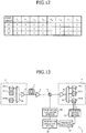
- FIG. 16 and FIG. 17 are diagrams illustrating the configuration of the main part of the polarization fluctuation compensation device applied to an optical communication system of the third embodiment, together with a configuration example of optical receivers 44-1 to 44-N.
- FIG. 16 is an application example corresponding to the digital coherent receiver illustrated in FIG. 2
- FIG. 17 is an application example corresponding to the direct detection receiver illustrated in FIG. 5 .
- the configuration of the entire optical communication system is the same as that illustrated in FIG. 1 , FIG. 13 , or FIG. 14 .
- a polarization fluctuation compensation device 5' applied to the third embodiment further includes a signal quality monitor 57 in addition to the configuration of the polarization fluctuation compensation device 5 in any one of the first and second embodiments.
- the signal quality monitor 57 monitors information related to the quality of a reception signal output from a signal processing section 408 ( FIG. 16 ) or signal processing sections 414X and 414Y ( FIG. 17 ) of the optical receivers 44-1 to 44-N, and feeds back the monitoring result to a parameter setting section 55.
- information related to the signal quality monitored by the signal quality monitor 57 for example; information of the number of error corrections detected at the time of error correction, a bit error rate (BER), or a ratio between average power and standard deviation of signal light monitored by a digital coherent receiver as described in Japanese Laid-Open Patent Publication No. 2009-198364 can be used.
- BER bit error rate
- FIG. 18 is a flowchart illustrating one example of an operation performed by the polarization fluctuation compensation device 5'.
- an information collection section 53 collects information related to the presence of polarization scrambling (or the speed of polarization fluctuations) in the optical signals having respective wavelengths (S210), and a parameter calculator 54 obtains a target value of the control parameter p by referring to the table illustrated in FIG. 8 or the like, or according to the relational expression shown in the flowchart of FIG. 11 , by using the information from the information collection section 53 (S220).
- a parameter setting section 55 sets a control parameter in the reception processing performed by the respective optical receivers 44-1 to 44-N, to the target value (S230).
- the signal quality monitor 57 monitors the information related to the quality of the reception signal output from the signal processing sections in the respective optical receivers 44-1 to 44-N.
- the parameter setting section 55 determines whether the signal quality of the respective wavelengths monitored by the signal quality monitor 57 satisfies a preset reference value. When the signal quality satisfies the reference value, the value of the current control parameter value is maintained. On the other hand, when the signal quality does not satisfy the reference value, control proceeds to step 260.
- step 260 the parameter setting section 55 changes the value of the control parameter set in the optical receiver so as to improve the signal quality monitored by the signal quality monitor 57, and control returns to step 240.
- the control parameter when the target value of the control parameter obtained in step 220 is ⁇ j , for example, the control parameter is sequentially changed to ⁇ j+1 , ⁇ j-1 , ⁇ j+2 , ⁇ j-2 , and so on, to search for a value at which the signal quality satisfies the reference value near the target value ⁇ j .
- the number of candidate values of the control parameter is limited, such a value at which the signal quality satisfies the reference value for all the candidate values can be searched.
- the optical communication system of the third embodiment because setting of the control parameter is feedback controlled according to the actual reception signal quality in the respective optical receivers 44-1 to 44-N, in addition to setting the control parameter with respect to the respective optical receivers 44-1 to 44-N in a feed forward manner according to the target value obtained by the parameter calculator 54 of the polarization fluctuation compensation device 5', compensation of the polarization fluctuations can be more reliably performed.
Landscapes
- Physics & Mathematics (AREA)
- Electromagnetism (AREA)
- Engineering & Computer Science (AREA)
- Computer Networks & Wireless Communication (AREA)
- Signal Processing (AREA)
- Nonlinear Science (AREA)
- Optical Communication System (AREA)
Claims (11)
- Ausgleichsvorrichtung (5) für Polarisationsfluktuationen, die betreibbar ist, um eine Qualitätsverschlechterung einer Signalwellenform auszugleichen, die bei einer Empfangsverarbeitung von WDM-Licht auftritt, das eine Vielzahl optischer Signale mit verschiedenen Wellenlängen enthält, umfassend:eine Informationssammelschaltung (53), die dafür angepasst ist, auf die Geschwindigkeit von Polarisationsfluktuationen in optischen Signalen mit jeweiligen Wellenlängen bezogene Information zu sammeln;eine Parameterrechnerschaltung (54), die dafür angepasst ist, einen Zielwert eines Steuerungsparameters entsprechend jeder Wellenlänge zu erhalten, basierend auf einer durch die Informationssammelschaltung (53) gesammelten Information, so dass ein Steuerungsparameter in der Empfangsverarbeitung bezogen auf eine Polarisationsinformation der optischen Signale mit jeweiligen Wellenlängen einen verschiedenen Wert gemäß der Geschwindigkeit von Polarisationsfluktuationen in den optischen Signalen mit jeweiligen Wellenlängen annimmt; undeine Parameterfestlegungsschaltung (55), die dafür angepasst ist, den durch die Parameterrechnerschaltung (54) erhaltenen Zielwert als den Steuerungsparameter in der Empfangsverarbeitung entsprechend den jeweiligen Wellenlängen festzulegen, wobeidas WDM-Licht ein einer Polarisationsverwürfelung unterzogenes optisches Signal und ein keiner Polarisationsverwürfelung unterzogenes optisches Signal enthält,die Informationssammelschaltung (53) dafür angepasst ist, Information zu sammeln, die auf das Vorhandensein einer Polarisationsverwürfelung entsprechend jeder Wellenlänge des WDM-Lichts bezogen ist,die Parameterrechnerschaltung (54) dafür angepasst ist, die Geschwindigkeit von Polarisationsfluktuationen in dem keiner Polarisationsverwürfelung unterzogenen optischen Signal zu bestimmen, basierend auf einer durch die Informationssammelschaltung (53) gesammelten Information, um einen Zielwert des Steuerungsparameters für einen optischen Empfänger (4) entsprechend dem keiner Polarisationsverwürfelung unterzogenen optischen Signal gemäß dem Bestimmungsergebnis zu erhalten, unddie Parameterfestlegungsschaltung (55) dafür angepasst ist, den durch die Parameterrechnerschaltung erhaltenen Zielwert als einen Steuerungsparameter für den optischen Empfänger (4) entsprechend dem keiner Polarisationsverwürfelung unterzogenen optischen Signal festzulegen.
- Ausgleichsvorrichtung (5) für Polarisationsfluktuationen nach Anspruch 1, wobei vorgesehen ist:ein Teiler (51), der dafür angepasst ist, einen Teil des WDM-Lichts als Überwachungslicht zu extrahieren; undein Detektor (52) für eine Polarisationsverwürfelung, der dafür angepasst ist, zu detektieren, ob ein optisches Signal jeder Wellenlänge, das in dem durch den Teiler (51) extrahierten Überwachungslicht enthalten ist, einer Polarisationsverwürfelung unterzogen wurde, und wobeidie Informationssammelschaltung (53) dafür angepasst ist, eine Information zu sammeln, die auf das durch den Detektor (52) für eine Polarisationsverwürfelung detektierte Vorhandensein einer Polarisationsverwürfelung in dem optischen Signal jeder Wellenlänge bezogen ist.
- Ausgleichsvorrichtung (5) für Polarisationsfluktuationen, die betreibbar ist, um eine Qualitätsverschlechterung einer Signalwellenform auszugleichen, die bei einer Empfangsverarbeitung von WDM-Licht auftritt, das eine Vielzahl optischer Signale mit verschiedenen Wellenlängen enthält, umfassend:eine Informationssammelschaltung (53), die dafür angepasst ist, Information zu sammeln, die auf die Geschwindigkeit von Polarisationsfluktuationen in optischen Signalen mit jeweiligen Wellenlängen bezogen ist;eine Parameterrechnerschaltung (54), die dafür angepasst ist, einen Zielwert eines Steuerungsparameters entsprechend jeder Wellenlänge zu erhalten, basierend auf einer durch die Informationssammelschaltung (53) gesammelten Information, so dass ein Steuerungsparameter in der Empfangsverarbeitung bezogen auf eine Polarisationsinformation der optischen Signale mit jeweiligen Wellenlängen einen verschiedenen Wert gemäß der Geschwindigkeit von Polarisationsfluktuationen in den optischen Signalen mit jeweiligen Wellenlängen annimmt; undeine Parameterfestlegungsschaltung (55), die dafür angepasst ist, den durch die Parameterrechnerschaltung (54) erhaltenen Zielwert als den Steuerungsparameter in der Empfangsverarbeitung entsprechend den jeweiligen Wellenlängen festzulegen, wobeidas WDM-Licht ein einer Polarisationsverwürfelung unterzogenes optisches Signal und ein keiner Polarisationsverwürfelung unterzogenes optisches Signal enthält, unddie Parameterrechnerschaltung (54) eine Tabelle aufweist, in der ein Zielwert des Steuerungsparameters entsprechend einer Kombination eines einer Polarisationsverwürfelung unterzogenen optischen Signals und eines keiner Polarisationsverwürfelung unterzogenen optischen Signals mit jeweiligen Wellenlängen festgelegt ist, und dafür eingerichtet ist, den Zielwert des Steuerungsparameters entsprechend der durch die Informationssammelschaltung (53) gesammelten Information zu bestimmen, indem auf die Tabelle Bezug genommen wird.
- Ausgleichsvorrichtung (5) für Polarisationsfluktuationen, die betreibbar ist, um eine Qualitätsverschlechterung einer Signalwellenform auszugleichen, die bei einer Empfangsverarbeitung eines WDM-Lichts auftritt, das eine Vielzahl optischer Signale mit verschiedenen Wellenlängen enthält, umfassend:eine Informationssammelschaltung (53), die dafür angepasst ist, Information zu sammeln, die auf die Geschwindigkeit von Polarisationsfluktuationen in optischen Signalen mit jeweiligen Wellenlängen bezogen ist;eine Parameterrechnerschaltung (54), die dafür angepasst ist, einen Zielwert eines Steuerungsparameters entsprechend jeder Wellenlänge zu erhalten, basierend auf einer durch die Informationssammelschaltung (53) gesammelten Information, so dass ein Steuerungsparameter in der Empfangsverarbeitung bezogen auf eine Polarisationsinformation der optischen Signale mit jeweiligen Wellenlängen einen verschiedenen Wert gemäß der Geschwindigkeit von Polarisationsfluktuationen in den optischen Signalen mit jeweiligen Wellenlängen annimmt; undeine Parameterfestlegungsschaltung (55), die dafür angepasst ist, den durch die Parameterrechnerschaltung (54) erhaltenen Zielwert als den Steuerungsparameter in der Empfangsverarbeitung entsprechend den jeweiligen Wellenlängen festzulegen, wobeidas WDM-Licht ein einer Polarisationsverwürfelung unterzogenes optisches Signal und ein keiner Polarisationsverwürfelung unterzogenes optisches Signal enthält, unddie Parameterrechnerschaltung (54) dafür eingerichtet ist, eine Suche durchzuführen, ob es ein einer Polarisationsverwürfelung unterzogenes optisches Signal in zumindest einem Wellenlängenbereich gibt, der basierend auf der Wellenlänge eines keiner Polarisationsverwürfelung unterzogenen optischen Signals festgelegt ist, gemäß einer arithmetischen Verarbeitung unter Verwendung einer durch die Informationssammelschaltung (53) gesammelten Information, und den Zielwert des Steuerungssignals gemäß dem Suchergebnis zu bestimmen.
- Ausgleichsvorrichtung (5) für Polarisationsfluktuationen nach einem der Ansprüche 1, 3 und 4, ferner umfassend einen digitalen kohärenten Empfänger (4), der dafür eingerichtet ist, das keiner Polarisationsverwürfelung unterzogene optische Signal zu verarbeiten.
- Ausgleichsvorrichtung (5) für Polarisationsfluktuationen nach Anspruch 5, wobei die Parameterrechnerschaltung (54) dafür eingerichtet ist, den Zielwert des Steuerungssignals als den Steuerungsparameter zu erhalten, durch Festlegen einer Schrittgröße eines digitalen Filters in einer arithmetischen Verarbeitung zum Restrukturieren einer Polarisationsinformation, die von dem digitalen kohärenten Empfänger durchgeführt werden soll.
- Ausgleichsvorrichtung (5) für Polarisationsfluktuationen nach einem der Ansprüche 1, 3 und 4, ferner umfassend einen Direktdetektionsempfänger, der dafür eingerichtet ist, das keiner Polarisationsverwürfelung unterzogene optische Signal zu verarbeiten.
- Ausgleichsvorrichtung für Polarisationsfluktuationen nach Anspruch 7, wobei die Parameterrechnerschaltung (54) dafür eingerichtet ist, den Zielwert des Steuerungssignals als den Steuerungsparameter zu erhalten, durch Festlegen einer Schleifenverstärkung in einer Rückkopplungssteuerung einer Polarisations-Steuerung (411), die von dem Direktdetektionsempfänger durchgeführt werden soll.
- Ausgleichsvorrichtung (5) für Polarisationsfluktuationen nach einem der vorhergehenden Ansprüche, ferner umfassend:eine Signalqualitätsüberwachungseinrichtung (57), die dafür eingerichtet ist, eine auf eine Qualität des optischen Signals jeder Wellenlänge bezogene Information zu überwachen, wobeidie Parameterfestlegungsschaltung (55) dafür eingerichtet ist, zu bestimmen, ob die Qualität eines Empfangssignals entsprechend jeder Wellenlänge einen Referenzwert erfüllt, basierend auf einer durch die Signalqualitätsüberwachungseinrichtung (57) überwachten Information, und einen festgelegten Wert des Steuerungsparameters so zu ändern, dass die Qualität des optischen Signals, welche den Referenzwert nicht erfüllt, den Referenzwert für eine Wellenlänge erfüllt.
- Optisches Kommunikationssystem, das enthält:eine optische Übertragungsvorrichtung (1), die dafür eingerichtet ist, WDM-Licht, das eine Vielzahl optischer Signale mit verschiedenen Wellenlängen enthält, zu einer optischen Übertragungsleitung (2) übertragen;eine optische Empfangsvorrichtung (4), die dafür eingerichtet ist, das auf der optischen Übertragungsleitung (2) übertragene WDM-Licht zu empfangen; undeine Ausgleichsvorrichtung (5) für Polarisationsfluktuationen nach einem der vorhergehenden Ansprüche.
- Optisches Kommunikationssystem nach Anspruch 10, umfassend zumindest einen auf der optischen Übertragungsleitung (2) angeordneten optischen Verstärker (3), wobei
die optische Übertragungsvorrichtung (1) eine Vielzahl optischer Transmitter (11-1 bis 11-M, 14-1 bis 14-N), einen Polarisationsverwürfler (13), in den ein Teil einer Vielzahl optischer Signale mit verschiedenen Wellenlängen eingegeben wird, die von der Vielzahl optischer Transmitter abgegeben werden, und einen Multiplexer (16) enthält, der dafür eingerichtet ist, ein optisches Signal, das durch den Polarisationsverwürfler (13) einer Polarisationsverwürfelung unterzogen wurde, und verbleibende, keiner Polarisationsverwürfelung unterzogenen optischen Signale zu multiplexen, und
die optische Empfangsvorrichtung (4) einen Demultiplexer (42), der dafür eingerichtet ist, WDM-Licht zu demultiplexen, das durch die optische Übertragungsleitung (2) und den optischen Verstärker (3) wiederholt übertragen wird, zumindest einen optischen Empfänger (43-1 bis 43-M), der dafür eingerichtet ist, ein einer Polarisationsverwürfelung unterzogenes optisches Signal der optischen Signale mit jeweiligen Wellenlängen zu empfangen, die vom Demultiplexer (42) abgegeben werden, und zumindest einen optischen Empfänger (44-1 bis 44-N) enthält, der dafür eingerichtet ist, ein keiner Polarisationsverwürfelung unterzogenes optisches Signal der optischen Signale mit jeweiligen Wellenlängen zu empfangen, die vom Demultiplexer (42) abgegeben werden.
Applications Claiming Priority (1)
| Application Number | Priority Date | Filing Date | Title |
|---|---|---|---|
| JP2010088469A JP5549333B2 (ja) | 2010-04-07 | 2010-04-07 | 偏波変動補償装置および光通信システム |
Publications (2)
| Publication Number | Publication Date |
|---|---|
| EP2375591A1 EP2375591A1 (de) | 2011-10-12 |
| EP2375591B1 true EP2375591B1 (de) | 2017-06-21 |
Family
ID=44279742
Family Applications (1)
| Application Number | Title | Priority Date | Filing Date |
|---|---|---|---|
| EP11160179.5A Not-in-force EP2375591B1 (de) | 2010-04-07 | 2011-03-29 | Ausgleichsvorrichtung für die Polarisierungsfluktuation und optisches Kommunikationssystem |
Country Status (3)
| Country | Link |
|---|---|
| US (1) | US8731411B2 (de) |
| EP (1) | EP2375591B1 (de) |
| JP (1) | JP5549333B2 (de) |
Families Citing this family (17)
| Publication number | Priority date | Publication date | Assignee | Title |
|---|---|---|---|---|
| JP5549333B2 (ja) * | 2010-04-07 | 2014-07-16 | 富士通株式会社 | 偏波変動補償装置および光通信システム |
| EP2506478A1 (de) * | 2011-03-25 | 2012-10-03 | Alcatel Lucent | Verfahren zur optischen Datenübertragung unter Anwendung von Polarisationsmultiplexierung |
| ES2605306T3 (es) * | 2011-05-31 | 2017-03-13 | Huawei Technologies Co., Ltd. | Método y dispositivo para procesar señales ópticas |
| WO2013114629A1 (ja) | 2012-02-03 | 2013-08-08 | 富士通株式会社 | 光伝送システムおよび光信号伝送方法 |
| WO2013128944A1 (ja) * | 2012-03-02 | 2013-09-06 | 日本電気株式会社 | 受信器、伝送システム、偏波多重光信号の受信方法、受信器の制御プログラムが格納された非一時的なコンピュータ可読媒体 |
| US9020364B2 (en) * | 2012-09-27 | 2015-04-28 | Alcatel Lucent | Optical receiver having a signal-equalization capability |
| JP2014096663A (ja) * | 2012-11-08 | 2014-05-22 | Fujitsu Ltd | 光伝送システム、光送信器、光受信器及び光伝送方法 |
| JP6065099B2 (ja) | 2013-02-26 | 2017-01-25 | 日本電気株式会社 | 波長分割多重光送信装置及び波長分割多重光送信方法 |
| US9319137B2 (en) * | 2013-09-09 | 2016-04-19 | Ciena Corporation | Methods and systems for reduced complexity nonlinear compensation |
| US9515745B2 (en) * | 2014-03-06 | 2016-12-06 | Cisco Technology, Inc. | Adaptive equalization in coherent receivers using a Stokes space update algorithm |
| US9577780B2 (en) * | 2014-06-26 | 2017-02-21 | Luxtera, Inc. | Method and system for a polarization immune wavelength division multiplexing demultiplexer |
| CN107819511B (zh) * | 2016-09-13 | 2020-03-06 | 富士通株式会社 | 残余直流分量的测量方法、装置和系统 |
| US11095390B2 (en) * | 2018-08-23 | 2021-08-17 | International Business Machines Corporation | Polarization-insensitive optical link |
| JP7057506B2 (ja) * | 2018-09-11 | 2022-04-20 | 日本電信電話株式会社 | デジタルコヒーレント受信器及びデジタルコヒーレント受信方法 |
| JP7059903B2 (ja) * | 2018-11-14 | 2022-04-26 | 富士通株式会社 | 通信装置、及び通信方法 |
| WO2021205786A1 (ja) * | 2020-04-07 | 2021-10-14 | 日本電気株式会社 | 偏波変動推定装置及び偏波変動推定方法 |
| WO2022265870A1 (en) * | 2021-06-17 | 2022-12-22 | Phyzhon Health Inc. | Optical system and method for performing a diagnostic check for optical signal quality |
Family Cites Families (52)
| Publication number | Priority date | Publication date | Assignee | Title |
|---|---|---|---|---|
| GB8630959D0 (en) * | 1986-12-29 | 1987-02-04 | British Telecomm | Optical polarisation control |
| JPH063511B2 (ja) * | 1987-10-27 | 1994-01-12 | 日本電気株式会社 | 光ヘテロダイン・ホモダイン検波方法 |
| JPH03214939A (ja) * | 1990-01-19 | 1991-09-20 | Nec Corp | チャンネル識別受信方法 |
| IT1239609B (it) * | 1990-05-11 | 1993-11-11 | Bordoni Ugo Fondazione | Metodo per la formazione di un segnale multilivello su una portante ottica coerente mediante modulazione di fase e di polarizzazione della portante e apparato di trasmissione e di ricezione eterodina di segnali formati con tale metodo |
| EP0772313A3 (de) * | 1990-09-14 | 1997-09-03 | Fujitsu Ltd | Optisches Kommunikationssystem mit gemultiplexten Unterträgern |
| US5111322A (en) | 1991-04-04 | 1992-05-05 | At&T Bell Laboratories | Polarization multiplexing device with solitons and method using same |
| JP3183685B2 (ja) * | 1991-09-13 | 2001-07-09 | 富士通株式会社 | 光通信システム |
| NL9200748A (nl) * | 1992-04-23 | 1993-11-16 | Nederland Ptt | Optische signaaloverdracht met polarisatie-ongevoelige coherente detectie en frekwentiestabilisatie aan de ontvangstzijde. |
| JPH05327576A (ja) | 1992-05-15 | 1993-12-10 | Nippon Telegr & Teleph Corp <Ntt> | ダイバーシチ送受信方式 |
| JP3751667B2 (ja) * | 1995-11-17 | 2006-03-01 | 富士通株式会社 | 偏波スクランブル式波長多重信号伝送方法 |
| US5930414A (en) * | 1997-09-16 | 1999-07-27 | Lucent Technologies Inc. | Method and apparatus for automatic compensation of first-order polarization mode dispersion (PMD) |
| US6604871B2 (en) * | 1997-09-19 | 2003-08-12 | Siemens Information And Communications Networks, Inc. | Method and apparatus for compensating for polarization mode dispersion (PMD) using a Mach-Zender interferometer |
| JP3939003B2 (ja) * | 1998-02-20 | 2007-06-27 | 富士通株式会社 | 同期偏波スクランブラを用いた光通信システム及び光受信装置 |
| US6385357B1 (en) * | 1999-08-23 | 2002-05-07 | Lucent Technologies Inc. | Method and apparatus for compensating for higher order paid PMD in a fiber transmission system at the fiber output |
| JP3557134B2 (ja) * | 1999-09-28 | 2004-08-25 | 富士通株式会社 | 光送信装置、波長分割多重方式光信号生成方法およびチャネル増設方法 |
| US6459830B1 (en) * | 2000-02-08 | 2002-10-01 | Sprint Communications Company L.P. | Method and apparatus to compensate for polarization mode dispersion |
| US6577413B1 (en) * | 2000-03-03 | 2003-06-10 | Pirelli Cavi E Sistemi S.P.A. | Method and apparatus for polarization multiplexing and demultiplexing optical tributary signals |
| JP2002009699A (ja) * | 2000-06-26 | 2002-01-11 | Kdd Submarine Cable Systems Inc | 受信信号の弁別閾値を決定する方法及び装置並びに光伝送システム |
| US6522796B1 (en) * | 2000-10-24 | 2003-02-18 | Jds Uniphase Corporation | Depolarizing polarization mode combiner |
| US6891674B2 (en) * | 2000-12-07 | 2005-05-10 | Yafo Networks, Inc. | Methods and apparatus for frequency shifting polarization mode dispersion spectra |
| KR100414456B1 (ko) * | 2001-03-07 | 2004-01-07 | 테라링크 커뮤니케이션스(주) | 광통신망에서 편광모드분산 및 색분산 감시장치 및 방법 |
| US7206517B1 (en) * | 2001-03-16 | 2007-04-17 | University Of Southern California (La) | Monitoring and in-line compensation of polarization dependent loss for lightwave systems |
| JP2002344426A (ja) | 2001-05-18 | 2002-11-29 | Kansai Electric Power Co Inc:The | 偏光状態制御信号の送受信方法および送受信装置 |
| JP2003060576A (ja) * | 2001-08-22 | 2003-02-28 | Nec Corp | 偏波スクランブラユニット及びこれを用いた多中継伝送システム |
| US6999688B1 (en) * | 2001-12-20 | 2006-02-14 | Sprint Communications Company L.P. | Optical systems with diversity detection |
| US6959152B2 (en) * | 2002-02-22 | 2005-10-25 | Nippon Telegraph And Telephone Corporation | Polarization scrambler and optical network using the same |
| EP1367743B1 (de) * | 2002-05-29 | 2007-07-25 | Alcatel Lucent | Polarisationsmodendispersionkompensator |
| US7391977B2 (en) * | 2003-03-12 | 2008-06-24 | General Photonics Corporation | Monitoring mechanisms for optical systems |
| KR100501544B1 (ko) * | 2003-04-08 | 2005-07-18 | 한국과학기술원 | 편광효과에 의한 시스템 열화의 저감방법 및 장치 |
| JP4612633B2 (ja) * | 2003-09-04 | 2011-01-12 | ドイッチェ テレコム アーゲー | 光伝送システムのpmd誘導性の障害確率の決定のための処理法およびデバイス |
| JP4167630B2 (ja) * | 2004-07-09 | 2008-10-15 | 富士通株式会社 | 光波長多重伝送システムにおける偏波モード分散補償装置および方法 |
| US20060029398A1 (en) | 2004-08-06 | 2006-02-09 | Li Liu | Transmission of optical signals of different modulation formats in discrete bands |
| US7317200B2 (en) | 2005-02-23 | 2008-01-08 | Micron Technology, Inc. | SnSe-based limited reprogrammable cell |
| CN101167273B (zh) * | 2005-04-29 | 2012-07-04 | 澳大利亚国家Ict有限公司 | 用于带内光学性能监测的方法及设备 |
| US8229302B2 (en) * | 2005-12-29 | 2012-07-24 | Ericsson Telecommunications S.A. | Method and arrangement for polarization mode dispersion mitigation |
| EP1811695A1 (de) * | 2006-01-20 | 2007-07-25 | Alcatel Lucent | Optischer Signalregenerator und Übertragungssystem |
| JP4750613B2 (ja) * | 2006-04-21 | 2011-08-17 | 富士通株式会社 | 偏波スクランブラ,光分岐挿入装置,光方路切換装置および波長分割多重光伝送システム |
| US7995918B2 (en) * | 2006-10-31 | 2011-08-09 | Alcatel Lucent | Polarization mode dispersion monitoring and fault correlation |
| JP4738315B2 (ja) * | 2006-11-02 | 2011-08-03 | 富士通株式会社 | 光信号処理装置、光信号伝送システム及び光信号処理方法 |
| KR100770882B1 (ko) * | 2006-11-10 | 2007-10-26 | 삼성전자주식회사 | 광수신 장치 및 이를 이용한 광통신 시스템 |
| JP5034770B2 (ja) * | 2007-08-16 | 2012-09-26 | 富士通株式会社 | コヒーレント光受信器および光通信システム |
| US7873286B2 (en) * | 2007-10-19 | 2011-01-18 | Ciena Corporation | Optical receiver systems and methods for polarization demultiplexing, PMD compensation, and DXPSK demodulation |
| JP5136761B2 (ja) | 2007-11-30 | 2013-02-06 | 株式会社三洋物産 | 遊技機 |
| JP5018453B2 (ja) * | 2007-12-19 | 2012-09-05 | 富士通株式会社 | 波長多重伝送システム |
| US8032022B2 (en) * | 2008-02-06 | 2011-10-04 | At&T Intellectual Property Ii, L.P. | Method for lightpath monitoring in an optical routing network |
| JP2009198364A (ja) | 2008-02-22 | 2009-09-03 | Fujitsu Ltd | 光ファイバ伝送路の特性および光信号の品質をモニタするモニタ回路 |
| JP2010060656A (ja) * | 2008-09-01 | 2010-03-18 | Fujitsu Ltd | 偏光状態安定化方法及び装置、光信号処理システム |
| FR2938913A1 (fr) * | 2008-11-27 | 2010-05-28 | France Telecom | Mesure du retard de groupe differentiel d'une liaison par fibre optique |
| US8195046B2 (en) * | 2009-12-14 | 2012-06-05 | Verizon Patent And Licensing, Inc. | Measurement of polarization mode dispersion or differential group delay of an optical path |
| JP5350284B2 (ja) * | 2010-01-28 | 2013-11-27 | 株式会社日立製作所 | 光送受信システム及び光受信機 |
| JP5549333B2 (ja) * | 2010-04-07 | 2014-07-16 | 富士通株式会社 | 偏波変動補償装置および光通信システム |
| US8958702B2 (en) * | 2011-03-17 | 2015-02-17 | Fujitsu Limited | System and method for reducing interference of a polarization multiplexed signal |
-
2010
- 2010-04-07 JP JP2010088469A patent/JP5549333B2/ja not_active Expired - Fee Related
-
2011
- 2011-03-29 EP EP11160179.5A patent/EP2375591B1/de not_active Not-in-force
- 2011-03-31 US US13/064,567 patent/US8731411B2/en not_active Expired - Fee Related
Non-Patent Citations (1)
| Title |
|---|
| None * |
Also Published As
| Publication number | Publication date |
|---|---|
| JP5549333B2 (ja) | 2014-07-16 |
| US20110249971A1 (en) | 2011-10-13 |
| US8731411B2 (en) | 2014-05-20 |
| EP2375591A1 (de) | 2011-10-12 |
| JP2011223185A (ja) | 2011-11-04 |
Similar Documents
| Publication | Publication Date | Title |
|---|---|---|
| EP2375591B1 (de) | Ausgleichsvorrichtung für die Polarisierungsfluktuation und optisches Kommunikationssystem | |
| Yaman et al. | Nonlinear impairment compensation for polarization-division multiplexed WDM transmission using digital backward propagation | |
| JP4592887B2 (ja) | 波長分散を補償する方法及びシステム | |
| EP2106044B1 (de) | Optisches Übertragungssystem mit Vor-Kompensation und Nach-Kompensation von Wellenformverzerrung | |
| JP6485095B2 (ja) | 光伝送装置、光伝送システム、及び、偏波依存損失モニタ | |
| US8478135B2 (en) | Method and apparatus for polarization-division-multiplexed optical receivers | |
| JP3923373B2 (ja) | 自動分散補償装置および補償方法 | |
| US7382985B2 (en) | Electrical domain mitigation of polarization dependent effects in an optical communications system | |
| US20030123884A1 (en) | Monitoring optical dispersion based on vestigial side band optical filtering | |
| EP2648352B1 (de) | Verfahren zum Ausgleichen einer chromatischen Verteilung und zugehöriges Gerät | |
| US6573985B2 (en) | Wavelength dispersion measuring device and a method thereof | |
| Tanimura et al. | Coherent reception and 126 GHz bandwidth digital signal processing of CO-OFDM superchannel generated by fiber frequency conversion | |
| Renaudier et al. | Investigation on WDM nonlinear impairments arising from the insertion of 100-Gb/s coherent PDM-QPSK over legacy optical networks | |
| JP2013162182A (ja) | 光信号品質測定方法、光信号品質測定回路、光受信装置及び光伝送システム | |
| JP3771830B2 (ja) | 自動分散補償回路付き光波長多重伝送システム | |
| Mateo et al. | Nonlinearity compensation using very-low complexity backward propagation in dispersion managed links | |
| Diniz et al. | Hardware-efficient chromatic dispersion estimator based on parallel Gardner timing error detector | |
| EP1554822B1 (de) | Elektrische verringerung von polarisationsabhängigen effekten in einem optischen kommunikationssystem | |
| EP3957005B1 (de) | Heterodyner kramers-kronig-empfänger mit polarisationsdiversität und verfahren | |
| WO2014119270A1 (ja) | 光受信装置、光通信システム、光受信方法及び光受信装置の制御プログラムの記録媒体 | |
| Asif et al. | Logarithmic step-size based digital backward propagation in N-channel 112Gbit/s/ch DP-QPSK transmission | |
| JP4056846B2 (ja) | 分散モニタ装置、分散モニタ方法および自動分散補償システム | |
| Charlet et al. | Performance comparison of singly-polarized and polarisation-multiplexed coherent transmission at 10 Gbauds under linear impairments | |
| EP3133751A1 (de) | Verfahren zur nichtlinearitätskompensierung in optischen übertragungssystemen | |
| JP5492118B2 (ja) | Wdm信号一括コヒーレント受信器及び方法 |
Legal Events
| Date | Code | Title | Description |
|---|---|---|---|
| PUAI | Public reference made under article 153(3) epc to a published international application that has entered the european phase |
Free format text: ORIGINAL CODE: 0009012 |
|
| AK | Designated contracting states |
Kind code of ref document: A1 Designated state(s): AL AT BE BG CH CY CZ DE DK EE ES FI FR GB GR HR HU IE IS IT LI LT LU LV MC MK MT NL NO PL PT RO RS SE SI SK SM TR |
|
| AX | Request for extension of the european patent |
Extension state: BA ME |
|
| 17P | Request for examination filed |
Effective date: 20111123 |
|
| 17Q | First examination report despatched |
Effective date: 20130719 |
|
| REG | Reference to a national code |
Ref country code: DE Ref legal event code: R079 Ref document number: 602011038851 Country of ref document: DE Free format text: PREVIOUS MAIN CLASS: H04B0010148000 Ipc: H04B0010610000 |
|
| RIC1 | Information provided on ipc code assigned before grant |
Ipc: H04B 10/61 20130101AFI20170119BHEP Ipc: H04B 10/2507 20130101ALI20170119BHEP |
|
| GRAP | Despatch of communication of intention to grant a patent |
Free format text: ORIGINAL CODE: EPIDOSNIGR1 |
|
| INTG | Intention to grant announced |
Effective date: 20170228 |
|
| GRAS | Grant fee paid |
Free format text: ORIGINAL CODE: EPIDOSNIGR3 |
|
| GRAA | (expected) grant |
Free format text: ORIGINAL CODE: 0009210 |
|
| AK | Designated contracting states |
Kind code of ref document: B1 Designated state(s): AL AT BE BG CH CY CZ DE DK EE ES FI FR GB GR HR HU IE IS IT LI LT LU LV MC MK MT NL NO PL PT RO RS SE SI SK SM TR |
|
| REG | Reference to a national code |
Ref country code: GB Ref legal event code: FG4D |
|
| REG | Reference to a national code |
Ref country code: CH Ref legal event code: EP |
|
| REG | Reference to a national code |
Ref country code: IE Ref legal event code: FG4D |
|
| REG | Reference to a national code |
Ref country code: AT Ref legal event code: REF Ref document number: 903803 Country of ref document: AT Kind code of ref document: T Effective date: 20170715 |
|
| REG | Reference to a national code |
Ref country code: DE Ref legal event code: R096 Ref document number: 602011038851 Country of ref document: DE |
|
| REG | Reference to a national code |
Ref country code: NL Ref legal event code: MP Effective date: 20170621 |
|
| PG25 | Lapsed in a contracting state [announced via postgrant information from national office to epo] |
Ref country code: GR Free format text: LAPSE BECAUSE OF FAILURE TO SUBMIT A TRANSLATION OF THE DESCRIPTION OR TO PAY THE FEE WITHIN THE PRESCRIBED TIME-LIMIT Effective date: 20170922 Ref country code: HR Free format text: LAPSE BECAUSE OF FAILURE TO SUBMIT A TRANSLATION OF THE DESCRIPTION OR TO PAY THE FEE WITHIN THE PRESCRIBED TIME-LIMIT Effective date: 20170621 Ref country code: NO Free format text: LAPSE BECAUSE OF FAILURE TO SUBMIT A TRANSLATION OF THE DESCRIPTION OR TO PAY THE FEE WITHIN THE PRESCRIBED TIME-LIMIT Effective date: 20170921 Ref country code: LT Free format text: LAPSE BECAUSE OF FAILURE TO SUBMIT A TRANSLATION OF THE DESCRIPTION OR TO PAY THE FEE WITHIN THE PRESCRIBED TIME-LIMIT Effective date: 20170621 Ref country code: FI Free format text: LAPSE BECAUSE OF FAILURE TO SUBMIT A TRANSLATION OF THE DESCRIPTION OR TO PAY THE FEE WITHIN THE PRESCRIBED TIME-LIMIT Effective date: 20170621 |
|
| REG | Reference to a national code |
Ref country code: LT Ref legal event code: MG4D |
|
| REG | Reference to a national code |
Ref country code: AT Ref legal event code: MK05 Ref document number: 903803 Country of ref document: AT Kind code of ref document: T Effective date: 20170621 |
|
| PG25 | Lapsed in a contracting state [announced via postgrant information from national office to epo] |
Ref country code: LV Free format text: LAPSE BECAUSE OF FAILURE TO SUBMIT A TRANSLATION OF THE DESCRIPTION OR TO PAY THE FEE WITHIN THE PRESCRIBED TIME-LIMIT Effective date: 20170621 Ref country code: BG Free format text: LAPSE BECAUSE OF FAILURE TO SUBMIT A TRANSLATION OF THE DESCRIPTION OR TO PAY THE FEE WITHIN THE PRESCRIBED TIME-LIMIT Effective date: 20170921 Ref country code: RS Free format text: LAPSE BECAUSE OF FAILURE TO SUBMIT A TRANSLATION OF THE DESCRIPTION OR TO PAY THE FEE WITHIN THE PRESCRIBED TIME-LIMIT Effective date: 20170621 Ref country code: SE Free format text: LAPSE BECAUSE OF FAILURE TO SUBMIT A TRANSLATION OF THE DESCRIPTION OR TO PAY THE FEE WITHIN THE PRESCRIBED TIME-LIMIT Effective date: 20170621 Ref country code: NL Free format text: LAPSE BECAUSE OF FAILURE TO SUBMIT A TRANSLATION OF THE DESCRIPTION OR TO PAY THE FEE WITHIN THE PRESCRIBED TIME-LIMIT Effective date: 20170621 |
|
| PG25 | Lapsed in a contracting state [announced via postgrant information from national office to epo] |
Ref country code: RO Free format text: LAPSE BECAUSE OF FAILURE TO SUBMIT A TRANSLATION OF THE DESCRIPTION OR TO PAY THE FEE WITHIN THE PRESCRIBED TIME-LIMIT Effective date: 20170621 Ref country code: SK Free format text: LAPSE BECAUSE OF FAILURE TO SUBMIT A TRANSLATION OF THE DESCRIPTION OR TO PAY THE FEE WITHIN THE PRESCRIBED TIME-LIMIT Effective date: 20170621 Ref country code: CZ Free format text: LAPSE BECAUSE OF FAILURE TO SUBMIT A TRANSLATION OF THE DESCRIPTION OR TO PAY THE FEE WITHIN THE PRESCRIBED TIME-LIMIT Effective date: 20170621 Ref country code: EE Free format text: LAPSE BECAUSE OF FAILURE TO SUBMIT A TRANSLATION OF THE DESCRIPTION OR TO PAY THE FEE WITHIN THE PRESCRIBED TIME-LIMIT Effective date: 20170621 Ref country code: AT Free format text: LAPSE BECAUSE OF FAILURE TO SUBMIT A TRANSLATION OF THE DESCRIPTION OR TO PAY THE FEE WITHIN THE PRESCRIBED TIME-LIMIT Effective date: 20170621 |
|
| PG25 | Lapsed in a contracting state [announced via postgrant information from national office to epo] |
Ref country code: SM Free format text: LAPSE BECAUSE OF FAILURE TO SUBMIT A TRANSLATION OF THE DESCRIPTION OR TO PAY THE FEE WITHIN THE PRESCRIBED TIME-LIMIT Effective date: 20170621 Ref country code: PL Free format text: LAPSE BECAUSE OF FAILURE TO SUBMIT A TRANSLATION OF THE DESCRIPTION OR TO PAY THE FEE WITHIN THE PRESCRIBED TIME-LIMIT Effective date: 20170621 Ref country code: ES Free format text: LAPSE BECAUSE OF FAILURE TO SUBMIT A TRANSLATION OF THE DESCRIPTION OR TO PAY THE FEE WITHIN THE PRESCRIBED TIME-LIMIT Effective date: 20170621 Ref country code: IS Free format text: LAPSE BECAUSE OF FAILURE TO SUBMIT A TRANSLATION OF THE DESCRIPTION OR TO PAY THE FEE WITHIN THE PRESCRIBED TIME-LIMIT Effective date: 20171021 Ref country code: IT Free format text: LAPSE BECAUSE OF FAILURE TO SUBMIT A TRANSLATION OF THE DESCRIPTION OR TO PAY THE FEE WITHIN THE PRESCRIBED TIME-LIMIT Effective date: 20170621 |
|
| REG | Reference to a national code |
Ref country code: DE Ref legal event code: R097 Ref document number: 602011038851 Country of ref document: DE |
|
| PLBE | No opposition filed within time limit |
Free format text: ORIGINAL CODE: 0009261 |
|
| STAA | Information on the status of an ep patent application or granted ep patent |
Free format text: STATUS: NO OPPOSITION FILED WITHIN TIME LIMIT |
|
| PG25 | Lapsed in a contracting state [announced via postgrant information from national office to epo] |
Ref country code: DK Free format text: LAPSE BECAUSE OF FAILURE TO SUBMIT A TRANSLATION OF THE DESCRIPTION OR TO PAY THE FEE WITHIN THE PRESCRIBED TIME-LIMIT Effective date: 20170621 |
|
| 26N | No opposition filed |
Effective date: 20180322 |
|
| PG25 | Lapsed in a contracting state [announced via postgrant information from national office to epo] |
Ref country code: SI Free format text: LAPSE BECAUSE OF FAILURE TO SUBMIT A TRANSLATION OF THE DESCRIPTION OR TO PAY THE FEE WITHIN THE PRESCRIBED TIME-LIMIT Effective date: 20170621 |
|
| REG | Reference to a national code |
Ref country code: DE Ref legal event code: R119 Ref document number: 602011038851 Country of ref document: DE |
|
| REG | Reference to a national code |
Ref country code: CH Ref legal event code: PL |
|
| GBPC | Gb: european patent ceased through non-payment of renewal fee |
Effective date: 20180329 |
|
| PG25 | Lapsed in a contracting state [announced via postgrant information from national office to epo] |
Ref country code: MC Free format text: LAPSE BECAUSE OF FAILURE TO SUBMIT A TRANSLATION OF THE DESCRIPTION OR TO PAY THE FEE WITHIN THE PRESCRIBED TIME-LIMIT Effective date: 20170621 |
|
| REG | Reference to a national code |
Ref country code: BE Ref legal event code: MM Effective date: 20180331 |
|
| REG | Reference to a national code |
Ref country code: IE Ref legal event code: MM4A |
|
| PG25 | Lapsed in a contracting state [announced via postgrant information from national office to epo] |
Ref country code: LU Free format text: LAPSE BECAUSE OF NON-PAYMENT OF DUE FEES Effective date: 20180329 |
|
| PG25 | Lapsed in a contracting state [announced via postgrant information from national office to epo] |
Ref country code: IE Free format text: LAPSE BECAUSE OF NON-PAYMENT OF DUE FEES Effective date: 20180329 Ref country code: DE Free format text: LAPSE BECAUSE OF NON-PAYMENT OF DUE FEES Effective date: 20181002 |
|
| PG25 | Lapsed in a contracting state [announced via postgrant information from national office to epo] |
Ref country code: LI Free format text: LAPSE BECAUSE OF NON-PAYMENT OF DUE FEES Effective date: 20180331 Ref country code: CH Free format text: LAPSE BECAUSE OF NON-PAYMENT OF DUE FEES Effective date: 20180331 Ref country code: BE Free format text: LAPSE BECAUSE OF NON-PAYMENT OF DUE FEES Effective date: 20180331 Ref country code: GB Free format text: LAPSE BECAUSE OF NON-PAYMENT OF DUE FEES Effective date: 20180329 |
|
| PG25 | Lapsed in a contracting state [announced via postgrant information from national office to epo] |
Ref country code: FR Free format text: LAPSE BECAUSE OF NON-PAYMENT OF DUE FEES Effective date: 20180331 |
|
| PG25 | Lapsed in a contracting state [announced via postgrant information from national office to epo] |
Ref country code: MT Free format text: LAPSE BECAUSE OF NON-PAYMENT OF DUE FEES Effective date: 20180329 |
|
| PG25 | Lapsed in a contracting state [announced via postgrant information from national office to epo] |
Ref country code: TR Free format text: LAPSE BECAUSE OF FAILURE TO SUBMIT A TRANSLATION OF THE DESCRIPTION OR TO PAY THE FEE WITHIN THE PRESCRIBED TIME-LIMIT Effective date: 20170621 |
|
| PG25 | Lapsed in a contracting state [announced via postgrant information from national office to epo] |
Ref country code: PT Free format text: LAPSE BECAUSE OF FAILURE TO SUBMIT A TRANSLATION OF THE DESCRIPTION OR TO PAY THE FEE WITHIN THE PRESCRIBED TIME-LIMIT Effective date: 20170621 Ref country code: HU Free format text: LAPSE BECAUSE OF FAILURE TO SUBMIT A TRANSLATION OF THE DESCRIPTION OR TO PAY THE FEE WITHIN THE PRESCRIBED TIME-LIMIT; INVALID AB INITIO Effective date: 20110329 |
|
| PG25 | Lapsed in a contracting state [announced via postgrant information from national office to epo] |
Ref country code: CY Free format text: LAPSE BECAUSE OF FAILURE TO SUBMIT A TRANSLATION OF THE DESCRIPTION OR TO PAY THE FEE WITHIN THE PRESCRIBED TIME-LIMIT Effective date: 20170621 Ref country code: MK Free format text: LAPSE BECAUSE OF NON-PAYMENT OF DUE FEES Effective date: 20170621 |
|
| PG25 | Lapsed in a contracting state [announced via postgrant information from national office to epo] |
Ref country code: AL Free format text: LAPSE BECAUSE OF FAILURE TO SUBMIT A TRANSLATION OF THE DESCRIPTION OR TO PAY THE FEE WITHIN THE PRESCRIBED TIME-LIMIT Effective date: 20170621 |