EP2369571B1 - Anzeigevorrichtung und Ansteuerungsverfahren dafür - Google Patents
Anzeigevorrichtung und Ansteuerungsverfahren dafür Download PDFInfo
- Publication number
- EP2369571B1 EP2369571B1 EP11003018A EP11003018A EP2369571B1 EP 2369571 B1 EP2369571 B1 EP 2369571B1 EP 11003018 A EP11003018 A EP 11003018A EP 11003018 A EP11003018 A EP 11003018A EP 2369571 B1 EP2369571 B1 EP 2369571B1
- Authority
- EP
- European Patent Office
- Prior art keywords
- voltage
- data line
- data
- display device
- circuit
- Prior art date
- Legal status (The legal status is an assumption and is not a legal conclusion. Google has not performed a legal analysis and makes no representation as to the accuracy of the status listed.)
- Not-in-force
Links
Images


Classifications
-
- G—PHYSICS
- G09—EDUCATION; CRYPTOGRAPHY; DISPLAY; ADVERTISING; SEALS
- G09G—ARRANGEMENTS OR CIRCUITS FOR CONTROL OF INDICATING DEVICES USING STATIC MEANS TO PRESENT VARIABLE INFORMATION
- G09G3/00—Control arrangements or circuits, of interest only in connection with visual indicators other than cathode-ray tubes
- G09G3/20—Control arrangements or circuits, of interest only in connection with visual indicators other than cathode-ray tubes for presentation of an assembly of a number of characters, e.g. a page, by composing the assembly by combination of individual elements arranged in a matrix no fixed position being assigned to or needed to be assigned to the individual characters or partial characters
- G09G3/22—Control arrangements or circuits, of interest only in connection with visual indicators other than cathode-ray tubes for presentation of an assembly of a number of characters, e.g. a page, by composing the assembly by combination of individual elements arranged in a matrix no fixed position being assigned to or needed to be assigned to the individual characters or partial characters using controlled light sources
- G09G3/30—Control arrangements or circuits, of interest only in connection with visual indicators other than cathode-ray tubes for presentation of an assembly of a number of characters, e.g. a page, by composing the assembly by combination of individual elements arranged in a matrix no fixed position being assigned to or needed to be assigned to the individual characters or partial characters using controlled light sources using electroluminescent panels
- G09G3/32—Control arrangements or circuits, of interest only in connection with visual indicators other than cathode-ray tubes for presentation of an assembly of a number of characters, e.g. a page, by composing the assembly by combination of individual elements arranged in a matrix no fixed position being assigned to or needed to be assigned to the individual characters or partial characters using controlled light sources using electroluminescent panels semiconductive, e.g. using light-emitting diodes [LED]
- G09G3/3208—Control arrangements or circuits, of interest only in connection with visual indicators other than cathode-ray tubes for presentation of an assembly of a number of characters, e.g. a page, by composing the assembly by combination of individual elements arranged in a matrix no fixed position being assigned to or needed to be assigned to the individual characters or partial characters using controlled light sources using electroluminescent panels semiconductive, e.g. using light-emitting diodes [LED] organic, e.g. using organic light-emitting diodes [OLED]
- G09G3/3275—Details of drivers for data electrodes
- G09G3/3291—Details of drivers for data electrodes in which the data driver supplies a variable data voltage for setting the current through, or the voltage across, the light-emitting elements
-
- G—PHYSICS
- G09—EDUCATION; CRYPTOGRAPHY; DISPLAY; ADVERTISING; SEALS
- G09G—ARRANGEMENTS OR CIRCUITS FOR CONTROL OF INDICATING DEVICES USING STATIC MEANS TO PRESENT VARIABLE INFORMATION
- G09G3/00—Control arrangements or circuits, of interest only in connection with visual indicators other than cathode-ray tubes
- G09G3/20—Control arrangements or circuits, of interest only in connection with visual indicators other than cathode-ray tubes for presentation of an assembly of a number of characters, e.g. a page, by composing the assembly by combination of individual elements arranged in a matrix no fixed position being assigned to or needed to be assigned to the individual characters or partial characters
- G09G3/22—Control arrangements or circuits, of interest only in connection with visual indicators other than cathode-ray tubes for presentation of an assembly of a number of characters, e.g. a page, by composing the assembly by combination of individual elements arranged in a matrix no fixed position being assigned to or needed to be assigned to the individual characters or partial characters using controlled light sources
- G09G3/30—Control arrangements or circuits, of interest only in connection with visual indicators other than cathode-ray tubes for presentation of an assembly of a number of characters, e.g. a page, by composing the assembly by combination of individual elements arranged in a matrix no fixed position being assigned to or needed to be assigned to the individual characters or partial characters using controlled light sources using electroluminescent panels
- G09G3/32—Control arrangements or circuits, of interest only in connection with visual indicators other than cathode-ray tubes for presentation of an assembly of a number of characters, e.g. a page, by composing the assembly by combination of individual elements arranged in a matrix no fixed position being assigned to or needed to be assigned to the individual characters or partial characters using controlled light sources using electroluminescent panels semiconductive, e.g. using light-emitting diodes [LED]
- G09G3/3208—Control arrangements or circuits, of interest only in connection with visual indicators other than cathode-ray tubes for presentation of an assembly of a number of characters, e.g. a page, by composing the assembly by combination of individual elements arranged in a matrix no fixed position being assigned to or needed to be assigned to the individual characters or partial characters using controlled light sources using electroluminescent panels semiconductive, e.g. using light-emitting diodes [LED] organic, e.g. using organic light-emitting diodes [OLED]
- G09G3/3225—Control arrangements or circuits, of interest only in connection with visual indicators other than cathode-ray tubes for presentation of an assembly of a number of characters, e.g. a page, by composing the assembly by combination of individual elements arranged in a matrix no fixed position being assigned to or needed to be assigned to the individual characters or partial characters using controlled light sources using electroluminescent panels semiconductive, e.g. using light-emitting diodes [LED] organic, e.g. using organic light-emitting diodes [OLED] using an active matrix
- G09G3/3233—Control arrangements or circuits, of interest only in connection with visual indicators other than cathode-ray tubes for presentation of an assembly of a number of characters, e.g. a page, by composing the assembly by combination of individual elements arranged in a matrix no fixed position being assigned to or needed to be assigned to the individual characters or partial characters using controlled light sources using electroluminescent panels semiconductive, e.g. using light-emitting diodes [LED] organic, e.g. using organic light-emitting diodes [OLED] using an active matrix with pixel circuitry controlling the current through the light-emitting element
-
- G—PHYSICS
- G09—EDUCATION; CRYPTOGRAPHY; DISPLAY; ADVERTISING; SEALS
- G09G—ARRANGEMENTS OR CIRCUITS FOR CONTROL OF INDICATING DEVICES USING STATIC MEANS TO PRESENT VARIABLE INFORMATION
- G09G2300/00—Aspects of the constitution of display devices
- G09G2300/08—Active matrix structure, i.e. with use of active elements, inclusive of non-linear two terminal elements, in the pixels together with light emitting or modulating elements
- G09G2300/0809—Several active elements per pixel in active matrix panels
- G09G2300/0819—Several active elements per pixel in active matrix panels used for counteracting undesired variations, e.g. feedback or autozeroing
-
- G—PHYSICS
- G09—EDUCATION; CRYPTOGRAPHY; DISPLAY; ADVERTISING; SEALS
- G09G—ARRANGEMENTS OR CIRCUITS FOR CONTROL OF INDICATING DEVICES USING STATIC MEANS TO PRESENT VARIABLE INFORMATION
- G09G2300/00—Aspects of the constitution of display devices
- G09G2300/08—Active matrix structure, i.e. with use of active elements, inclusive of non-linear two terminal elements, in the pixels together with light emitting or modulating elements
- G09G2300/0809—Several active elements per pixel in active matrix panels
- G09G2300/0842—Several active elements per pixel in active matrix panels forming a memory circuit, e.g. a dynamic memory with one capacitor
- G09G2300/0852—Several active elements per pixel in active matrix panels forming a memory circuit, e.g. a dynamic memory with one capacitor being a dynamic memory with more than one capacitor
-
- G—PHYSICS
- G09—EDUCATION; CRYPTOGRAPHY; DISPLAY; ADVERTISING; SEALS
- G09G—ARRANGEMENTS OR CIRCUITS FOR CONTROL OF INDICATING DEVICES USING STATIC MEANS TO PRESENT VARIABLE INFORMATION
- G09G2320/00—Control of display operating conditions
- G09G2320/02—Improving the quality of display appearance
- G09G2320/0233—Improving the luminance or brightness uniformity across the screen
-
- G—PHYSICS
- G09—EDUCATION; CRYPTOGRAPHY; DISPLAY; ADVERTISING; SEALS
- G09G—ARRANGEMENTS OR CIRCUITS FOR CONTROL OF INDICATING DEVICES USING STATIC MEANS TO PRESENT VARIABLE INFORMATION
- G09G2320/00—Control of display operating conditions
- G09G2320/02—Improving the quality of display appearance
- G09G2320/029—Improving the quality of display appearance by monitoring one or more pixels in the display panel, e.g. by monitoring a fixed reference pixel
- G09G2320/0295—Improving the quality of display appearance by monitoring one or more pixels in the display panel, e.g. by monitoring a fixed reference pixel by monitoring each display pixel
Definitions
- the present invention relates to display devices, more particularly, to display devices using an electric current driving element such as an organic EL display or an FED, and a method for driving the same.
- An organic EL element included in an organic EL display emits light at higher luminance as a voltage to be applied thereto is high and an electric current flowing therethrough is large in amount.
- a relation between the luminance and the voltage varies readily due to influences such as a driving time and an ambient temperature. Consequently, it becomes very difficult to suppress the variations in luminance of the organic EL element if a driving scheme of a voltage control type is adopted for the organic EL display.
- the luminance of the organic EL element is almost proportional to the electric current. This proportional relation is less susceptible to an influence of an extraneous factor such as an ambient temperature. Accordingly, it is preferable that a driving scheme of an electric current control type is adopted for the organic EL display.
- a display device includes a pixel circuit and a drive circuit each of which is configured using a TFT (Thin Film Transistor) made of amorphous silicon, low-temperature polycrystalline silicon, CG (Continuous Grain) silicon or the like.
- TFT Thin Film Transistor
- CG Continuous Grain
- a circuit that compensates the variations in characteristic of the TFT is provided for the pixel circuit of the organic EL display.
- the variations in luminance of the organic EL element are suppressed by action of this circuit.
- a scheme for compensating variations in characteristic of a TFT is broadly divided into an electric current program scheme in which an amount of an electric current flowing through a driving TFT is controlled by an electric current signal and a voltage program scheme in which the amount of this electric current is controlled by a voltage signal.
- Use of the electric current program scheme allows compensation of variations in threshold voltage and mobility.
- Use of the voltage program scheme allows compensation of only the variations in threshold voltage.
- the electric current program scheme has the following two problems. First, it is difficult to design a pixel circuit and a drive circuit since an electric current to be used herein is considerably small in amount. Second, it is difficult to make a large-area circuit since an influence of a parasitic capacity is exerted readily when an electric current signal is set. In contrast to this, according to the voltage program scheme, an influence of a parasitic capacity or the like is minute and a circuit is designed in a relatively ease manner. Moreover, an influence of variations in mobility to be exerted on an amount of an electric current is smaller than an influence of variations in threshold voltage to be exerted on the amount of the electric current. Further, the variations in mobility can be suppressed to a certain degree in a step of manufacturing a TFT. Accordingly, even a display device that adopts the voltage program scheme can provide satisfactory display quality.
- Fig. 11 is a circuit diagram showing a pixel circuit described in Patent Document 1.
- the pixel circuit 90 shown in Fig. 11 includes a driving TFT 91, switching TFTs 92 to 94, capacitors 95 and 96, and an organic EL element 97 (also referred to as an OLED (Organic Light Emitting Diode)).
- Each of the TFTs included in the pixel circuit 90 is of a P-channel type.
- the driving TFT 91, the switching TFT 94 and the organic EL element 97 are provided in series between a power supply wiring line Vp (potential: VDD) and a common cathode (GND).
- the capacitor 95 and the switching TFT 92 are provided in series between a gate terminal of the driving TFT 91 and a data line Sj.
- the switching TFT 93 is provided between the gate terminal and a drain terminal of the driving TFT 91, and the capacitor 96 is provided between the gate terminal of the driving TFT 91 and the power supply wiring line Vp.
- the switching TFT 92 has a gate terminal connected to a scanning line Gi
- the switching TFT 93 has a gate terminal connected to an auto-zero line AZi
- the switching TFT 94 has a gate terminal connected to an illumination line ILi.
- Fig. 12 is a timing chart showing a timing that data is written to the pixel circuit 90.
- a potential at the scanning line Gi and a potential at the auto-zero line AZi are controlled to a high level, respectively, a potential at the illumination line ILi is controlled to a low level, and a potential at the data line Sj is controlled to a reference potential Vstd.
- the switching TFT 92 is changed to a conduction state.
- the switching TFT 93 is changed to the conduction state.
- the driving TFT 91 thus, the gate terminal and the drain terminal become equal in potential to each other.
- the switching TFT 94 is changed to a non-conduction state.
- an electric current flows from the power supply wiring line Vp into the gate terminal of the driving TFT 91 via the driving TFT 91 and the switching TFT 93.
- the potential at the gate terminal of the driving TFT 91 rises during a period that the driving TFT 91 is in the conduction state.
- the driving TFT 91 is changed to the non-conduction state when a gate-source voltage becomes a threshold voltage Vth (negative value) (i.e., when the potential at the gate terminal becomes (VDD + Vth)). Accordingly, the potential at the gate terminal of the driving TFT 91 rises to (VDD + Vth).
- the switching TFT 94 is changed to the conduction state.
- an electric current flows from the power supply wiring line Vp into the organic EL element 97 via the driving TFT 91 and the switching TFT 94.
- An amount of the electric current flowing through the driving TFT 91 increases/decreases in accordance with the potential (VDD + Vth + Vdata - Vstd) at the gate terminal.
- the amount of the electric current is the same as long as the potential difference (Vdata - Vstd) is the same even when the threshold voltage Vth is different.
- the electric current flows through the organic EL element 97 in an amount which depends on the potential Vdata, so that the organic EL element 97 emits light at a luminance which depends on the data potential Vdata.
- Patent Document 2 describes the following method. That is, an electric current capability of a drive element is measured and is stored in a memory provided outside a pixel circuit, and a voltage to be supplied to a panel is changed in accordance with the stored electric current capability (see Fig. 13 ).
- Patent Document 3 describes the following method. That is, a switch for applying an initial voltage to one end of a coupling capacitance is provided for setting a threshold value correction period longer than a selection period.
- this pixel circuit (hereinafter, referred to as the conventional pixel circuit) has the following problems.
- a first problem is that an amplitude of a data voltage can not be utilized efficiently.
- data is written by capacitance coupling. Consequently, even when a certain data voltage is written from an outside of the pixel circuit, a voltage to be applied actually as an overdrive voltage to the driving TFT becomes Cc/ (Cc + Cs + Cgs) times as large as the written data voltage (where Cc represents a capacitance of the capacitor 95, Cs represents a capacitance of the capacitor 96 and Cgs represents a gate-source capacitance of the driving TFT 91).
- Cc represents a capacitance of the capacitor 95
- Cs represents a capacitance of the capacitor 96
- Cgs represents a gate-source capacitance of the driving TFT 91.
- the coupling capacitance Cc When the coupling capacitance Cc is set to be considerably large, the amplitude of the data voltage can be utilized efficiently.
- the pixel circuit is disadvantageously increased in scale.
- the parasitic capacitance Cgs which can not be controlled with high accuracy, exerts an adverse influence on a drive voltage.
- a second problem is that the threshold value correction is low in accuracy. As described above, since the actual drive voltage becomes Cc/ (Cc + Cs + Cgs) times as large as the voltage applied from the outside, an effect of the threshold value correction also becomes Cc/ (Cc + Cs + Cgs) times. Consequently, it is difficult to completely correct the threshold voltage.
- a third problem is that the pixel circuit is increased in scale. As described above, when the coupling capacitance Cc is increased in order to deal with the parasitic capacitance, an area occupied by the capacitor 95 becomes large in the layout of the pixel circuit. Consequently, an aperture ratio is reduced in an organic EL display having a bottom emission configuration in which light is extracted from a bottom side of a substrate. Moreover, since the increase in circuit area results in reduction of a yield in manufacturing, the area of the pixel circuit must be decreased and the number of elements in the pixel circuit must be reduced.
- a fourth problem is that an inspection in manufacturing becomes difficult.
- the gate terminal of the driving TFT is connected to the data line through the capacitor. Consequently, it is difficult to inspect the electric current, which flows through the driving TFT, via the data line. For this reason, it becomes difficult to improve a yield through to the inspection.
- a fifth problem is that the threshold value correction period is restricted to a short time.
- the threshold value correction and the data write must be performed within the period for selecting the pixel circuit.
- the threshold value correction requires a time until the gate-source voltage of the diode-connected drive element sufficiently approximates the threshold voltage.
- a selection period is very short. For example, in a case where a panel having a resolution of VGA is driven at 60 frames/s, a selection period is set at about 30 ⁇ s. It is difficult to complete threshold value correction and data write within this short time.
- the third problem can be solved.
- the memory for storing the electric current capability of each drive element is provided, a cost of a peripheral circuit and a layout area are increased.
- the fifth problem can be solved.
- the switch for applying the initial voltage is provided, the pixel circuit is further increased in scale.
- an object of the present invention is to provide a display device that efficiently utilizes an amplitude of a data voltage and performs threshold value correction with high accuracy, without increasing a scale of a pixel circuit.
- a first aspect of the present invention is a display device of an electric current driving type, including: a plurality of pixel circuits arranged in correspondence with intersections of a plurality of scanning lines and a plurality of data lines, each pixel circuit including an electro-optical element and a drive element having a control terminal connected to the data line through a switching element; a scanning signal output circuit selecting a write-target pixel circuit through use of the scanning line, and exercising control such that the selected pixel circuit outputs, to the data line, a voltage which depends on a threshold voltage of the drive element; and a display signal output circuit applying, to the data line, a voltage obtained by adding or subtracting a correction voltage corresponding to the threshold voltage to or from a data voltage corresponding to display data, based on the voltage outputted to the data line.
- a second aspect of the present invention is the display device according to the first aspect of the present invention, wherein the electro-optical element and the drive element are provided in series between two power supply wiring lines in the pixel circuit, and the pixel circuit further includes a first switching element connected to a control terminal of the drive element and the data line, a second switching element provided between the control terminal and one conductive terminal of the drive element, a third switching element provided together with the electro-optical element and the drive element in series between the power supply wiring lines, and a capacitance having one end connected to the control terminal of the drive element.
- a third aspect of the present invention is the display device according to the second aspect of the present invention, wherein the scanning signal output circuit controls the write-target pixel circuit such that the first and second switching elements are set at a conduction state, the third switching element is set at a non-conduction state, next, the second switching element is changed to the non-conduction state, then, the first switching element is changed to the non-conduction state and the third switching element is changed to the conduction state, and the display signal output circuit applies, to the data line, the voltage obtained by adding or subtracting the correction voltage to or from the data voltage after the second switching element is changed to the non-conduction state, based on a voltage of the data line in the case where the second switching element is in the conduction state.
- a fourth aspect of the present invention is the display device according to the second aspect of the present invention, wherein each of the drive element and the first to third switching elements is a thin film transistor, one of the first and third switching elements is of a P-channel type and the other switching element is of an N-channel type, and the first and third switching elements have control terminals connected to a common wiring line.
- a fifth aspect of the present invention is the display device according to the second aspect of the present invention, wherein each of the drive element and the first to third switching elements is a thin film transistor, one of the second and third switching elements is of a P-channel type and the other switching element is of an N-channel type, and the second and third switching elements have control terminals connected to a common wiring line.
- a sixth aspect of the present invention is the display device according to the second aspect of the present invention, wherein the drive element is an enhancement P-channel type transistor, and the pixel circuit selected by the scanning signal output circuit outputs, to the data line, a voltage obtained by subtracting an absolute value of the voltage which depends on the threshold voltage of the drive element from a higher one of voltages of the power supply wiring lines.
- a seventh aspect of the present invention is the display device according to the second aspect of the present invention, wherein the drive element is an enhancement N-channel type transistor, and the pixel circuit selected by the scanning signal output circuit outputs, to the data line, a voltage obtained by adding an absolute value of the voltage which depends on the threshold voltage of the drive element to a lower one of voltages of the power supply wiring lines.
- the drive element is an enhancement N-channel type transistor
- the pixel circuit selected by the scanning signal output circuit outputs, to the data line, a voltage obtained by adding an absolute value of the voltage which depends on the threshold voltage of the drive element to a lower one of voltages of the power supply wiring lines.
- An eighth aspect of the present invention is the display device according to the second aspect of the present invention, wherein the display signal output circuit applies a predetermined constant voltage to the data line at a part of a conduction period of the first switching element.
- a ninth aspect of the present invention is the display device according to the first aspect of the present invention, wherein the display signal output circuit includes a plurality of analog buffers, and a plurality of correcting capacitances and a plurality of switch circuits provided for each data line, and the switch circuit switches between a state that one electrode of the correcting capacitance is connected to the data line and the other electrode thereof is applied with a predetermined constant voltage and a state that one electrode of the correcting capacitance is connected to the data line through the analog buffer and the other electrode thereof is applied with the data voltage.
- the display signal output circuit includes a plurality of analog buffers, and a plurality of correcting capacitances and a plurality of switch circuits provided for each data line, and the switch circuit switches between a state that one electrode of the correcting capacitance is connected to the data line and the other electrode thereof is applied with a predetermined constant voltage and a state that one electrode of the correcting capacitance is connected to the data line through the analog buffer and the other electrode thereof is applied
- a tenth aspect of the present invention is the display device according to the ninth aspect of the present invention, wherein the analog buffer is provided for the plurality of data lines.
- An eleventh aspect of the present invention is a method for driving a display device including a plurality of pixel circuits arranged in correspondence with intersections of a plurality of scanning lines and a plurality of data lines, each pixel circuit including an electro-optical element and a drive element having a control terminal connected to the data line through a switching element, the method including the steps of: selecting a write-target pixel circuit through use of the scanning line, and exercising control such that the selected pixel circuit outputs, to the data line, a voltage which depends on a threshold voltage of the drive element; and applying, to the data line, a voltage obtained by adding or subtracting a correction voltage corresponding to the threshold voltage to or from a data voltage corresponding to display data, based on the voltage outputted to the data line.
- the first or eleventh aspect of the present invention it is possible to read the voltage which depends on the threshold voltage of the drive element from the selected pixel circuit and to apply, to the control terminal of the drive element, the voltage obtained by adding or subtracting the correction voltage (the voltage corresponding to the threshold voltage) to or from the data voltage. Accordingly, it is possible to detect the threshold voltage of the drive element to compensate variations in threshold voltage, and to allow the electro-optical element to emit light at a desired luminance. Moreover, the threshold value correction circuit is provided outside the pixel circuit and the threshold voltage is detected by use of the data line, leading to reduction in scale and area of the pixel circuit.
- the threshold voltage is detected as a voltage signal, so that a current-voltage conversion element becomes unnecessary unlike a case where an electric current signal is fed back. Therefore, variations in correction effect can be suppressed.
- a desired voltage is applied to the control terminal of the drive element through no coupling capacitance. Therefore, it is possible to efficiently utilize an amplitude of the data voltage and to reduce power consumption.
- the capacitance it is possible to reduce the capacitance to be used for threshold value correction, to improve an aperture ratio and a yield, and to reduce power consumption.
- the period for selecting the pixel circuit into a period for detecting the threshold voltage and a period for writing the corrected data voltage, and to allow commonality of a feedback line for reading the threshold voltage and a data line for writing the data.
- the fourth or fifth aspect of the present invention it is possible to reduce the number of wiring lines in such a manner that the first to third switching elements share the wiring line to be connected to the control terminals thereof. Thus, it is possible to make an aperture ratio of a pixel higher.
- the variations in threshold voltage can be compensated in the drive element of the P-channel type when the voltage obtained by subtraction of the absolute value of the threshold voltage is applied to the control terminal. Therefore, it is possible to compensate the variations in threshold voltage of the drive element by use of the voltage outputted from the selected pixel circuit.
- the variations in threshold voltage can be compensated in the drive element of the N-channel type when the voltage obtained by addition of the absolute value of the threshold voltage is applied to the control terminal. Therefore, it is possible to compensate the variations in threshold voltage of the drive element by use of the voltage outputted from the selected pixel circuit.
- the suitable constant voltage is applied to the control terminal of the drive element.
- it is possible to reduce a time which is required until the voltage which depends on the threshold voltage of the drive element is outputted to the data line. Accordingly, it is possible to suppress variations in correction effect and to improve image quality even when the threshold value correction period is short.
- the display signal output circuit can apply, to the data line, the voltage obtained by adding "the difference between the data voltage and the constant voltage" to the voltage of the data line. Accordingly, when the constant voltage is determined appropriately, the voltage obtained by adding or subtracting the correction voltage (the voltage corresponding to the threshold voltage of the drive element) to or from the data voltage can be applied to the data line, based on the voltage outputted from the pixel circuit to the data line. Moreover, this addition or subtraction is performed outside the pixel circuit, leading to reduction in scale of the pixel circuit. Further, the analog buffer is provided between the correcting capacitance and the data line. Thus, it is possible to suppress attenuation due to coupling of the voltage held at the correcting capacitance and to realize high image quality.
- the analog buffer having a large circuit scale is not arranged for each data line, but is arranged for the plurality of data lines.
- the display device to be described below includes a pixel circuit including an electro-optical element and a plurality of switching elements.
- the switching elements included in the pixel circuit may be a low-temperature polysilicon TFT, a CG silicon TFT, an amorphous silicon TFT, and the like. A configuration and a fabrication process of such a TFT are well-known; therefore, description thereof will not be given here.
- the electro-optical element included in the pixel circuit is an organic EL element. A configuration of such an organic EL element is also well-known; therefore, description thereof will not be given here.
- description will be given of a common overall configuration of the display devices according to the first to third embodiments. Thereafter, description will be given of a pixel circuit and a threshold value correction circuit in the display device according to each embodiment.
- Fig. 1 is a block diagram showing the configuration of the display devices according to the first to third embodiments of the present invention.
- the display device 1 shown in Fig. 1 includes a plurality of pixel circuits Aij (i: an integer in a range between 1 or more and n or less, j : an integer in a range between 1 or more and m or less) , a display control circuit 2, a gate driver circuit 3 and a source driver circuit 4.
- the gate driver circuit 3 functions as a scanning signal output circuit
- the source driver circuit 4 functions as a display signal output circuit.
- the display device 1 also includes a plurality of scanning lines Gi which are provided in parallel with one another, and a plurality of data lines Sj which are provided in parallel with one another so as to be orthogonal to the plurality of scanning lines Gi.
- the pixel circuits Aij are arranged in a matrix form in correspondence with intersections of the scanning lines Gi and the data lines Sj.
- a plurality of control lines Wi and a plurality of control lines Ri are arranged in parallel with the scanning lines Gi so as to be parallel with one another.
- the scanning lines Gi and the control lines Wi and Ri are connected to the gate driver circuit 3, and the data lines Sj are connected to the source driver circuit 4.
- a power supply wiring line Vp and a common cathode Vcom which are not shown in the figure, are arranged.
- cathode wiring lines CAi may be arranged in place of the common cathode Vcom.
- the display control circuit 2 outputs a timing signal OE, a start pulse YI and a clock YCK to the gate driver circuit 3, and outputs a start pulse SP, a clock CLK, display data DA and a latch pulse LP to the source driver circuit 4. Moreover, the display control circuit 2 controls potentials at control lines SCAN1 to SCAN3 of the source driver circuit 4.
- the gate driver circuit 3 includes a shift register circuit, a logic operation circuit and a buffer (each of which is not shown in the figure).
- the shift register circuit sequentially transfers the start pulse YI in synchronization with the clock YCK.
- the logic operation circuit performs a logic operation between a pulse outputted from each stage of the shift register circuit and the timing signal OE. An output from the logic operation circuit is given to each of the corresponding scanning line Gi and the corresponding control lines Wi and Ri via the buffer.
- “m" pixel circuits Aij are connected to one scanning line Gi.
- the "m” pixel circuits Aij are selected collectively by use of the scanning line Gi.
- the source driver circuit 4 includes an "m"-bit shift register 5, a register 6, a latch 7, "m” D/A converters 8 and "m” threshold value correction circuits 9.
- the source driver circuit 4 performs a line sequential scan wherein data is transmitted to the pixel circuits Aij in one row at a single timing. More specifically, the shift register 5 has cascade-connected "m" registers.
- the shift register 5 transfers the start pulse SP supplied to the register on a first stage in synchronization with the clock CLK, and outputs timing pulses DLP from the registers on the respective stages.
- the display data DA is supplied to the register 6 at an output timing of the timing pulse DLP.
- the register 6 stores the display data DA in accordance with the timing pulse DLP.
- the display control circuit 2 outputs the latch pulse LP to the latch 7.
- the latch 7 receives the latch pulse LP and then holds the display data stored in the register 6.
- the D/A converters 8 and the threshold value correction circuits 9 are provided in correspondence with the data lines Sj.
- the D/A converter 8 converts the display data held by the latch 7 to an analog signal voltage, and outputs the analog signal voltage to the corresponding threshold value correction circuit 9.
- the threshold value correction circuit 9 receives, via the data line Sj , a voltage outputted from the pixel circuit Aij selected by the gate driver circuit 3 (i.e. , a voltage which depends on a threshold voltage of a driving TFT). Based on this voltage, the threshold value correction circuit 9 applies, to the data line Sj, a voltage obtained by adding or subtracting a correction voltage corresponding to the threshold voltage of the driving TFT to or from the output voltage of the D/A converter 8.
- variations in threshold voltage of the driving TFT included in the pixel circuit Aij can be compensated by action of the threshold value correction circuit 9 (details thereof will be described later).
- the source driver circuit 4 may perform a dot sequential scan wherein data is sequentially transmitted to each pixel circuit.
- a dot sequential scan is performed, a voltage of the data line Sj is held by a capacitance of the data line Sj during a period that a certain scanning line Gi is selected.
- a configuration of the source driver circuit that performs such a dot sequential scan is well-known; therefore, description thereof will not be given here.
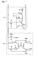
- Fig. 2 is a circuit diagram showing the pixel circuit and the threshold value correction circuit each included in the display device according to the first embodiment of the present invention.
- the pixel circuit 10 and the threshold value correction circuit 20 in Fig. 2 correspond to the pixel circuit Aij and the threshold value correction circuit 9 in Fig. 1 .
- the pixel circuit 10 includes a driving TFT 11, switching TFTs 12 to 14, an organic EL element 15 and a capacitor 16.
- the driving TFT 11 is of an enhancement P-channel type
- each of the switching TFTs 12 and 13 is of an N-channel type
- the switching TFT 14 is of a P-channel type.
- the pixel circuit 10 is connected to the power supply wiring line Vp, the common cathode Vcom, the scanning line Gi, the control line Wi, the control line Ri and the data line Sj.
- a potential at the power supply wiring line Vp is represented by VDD
- a potential at the common cathode Vcom is represented by VSS (herein, VDD > VSS).
- the common cathode Vcom serves as a common electrode of all the organic EL elements 15 in the display device.
- the driving TFT 11, the switching TFT 14 and the organic EL element 15 are provided in series between the power supply wiring line Vp and the common cathode Vcom sequentially from a side of the power supply wiring line Vp.
- the switching TFT 12 is provided between a gate terminal of the driving TFT 11 and the data line Sj.
- the switching TFT 13 is provided between the gate terminal and a drain terminal of the driving TFT 11, and the capacitor 16 is provided between the gate terminal of the driving TFT 11 and the power supply wiring line Vp.
- the switching TFT 12 has a gate terminal connected to the scanning line Gi
- the switching TFT 13 has a gate terminal connected to the control line Wi
- the switching TFT 14 has a gate terminal connected to the control line Ri.
- a potential at each of the scanning line Gi, the control line Wi and the control line Ri is controlled by the gate driver circuit 3, and a potential at the data line Sj is controlled by the source driver circuit 4.
- a node to be connected to the gate terminal of the driving TFT 11 is represented by A.
- the threshold value correction circuit 20 includes switches 21 to 25, a capacitor 26 and an analog buffer 27, and is connected to the data line Sj.
- Each of the switches 21 to 25 is an N-channel type transistor, and the analog buffer 27 is a voltage follower circuit (a unity gain amplifier).
- a node to be connected to a first electrode (an electrode illustrated at a right side in Fig. 2 ) of the capacitor 26 is represented by B, and a node to be connected to a second electrode of the capacitor 26 is represented by C.
- the switch 21 is provided between the data line Sj and the node C
- the switch 22 is provided between the node B and the power supply wiring line Vp.
- the switch 23 has a first end connected to the node B.
- the analog buffer 27 and the switch 24 are provided in series between the node C and the data line Sj sequentially from a side of the node C.
- the switch 25 has a first end connected to the data line Sj.
- the switch 23 has a second end to which the data voltage Vdata outputted from the D/A converter 8 is applied.
- the switch 25 has a second end to which an initial voltage Vreset (details thereof will be described later) is applied.
- the switches 21 and 22 have gate terminals connected to the control line SCAN2, respectively.
- the switches 23 and 24 have gate terminals connected to the control line SCAN1, respectively.
- the switch 25 has a gate terminal connected to the control line SCAN3.
- a threshold voltage of the driving TFT 11 is represented by Vth (negative value).
- the capacitor 26 functions as a correcting capacitance that holds a correction voltage Vx corresponding to the threshold voltage Vth of the driving TFT 11.
- the switches 21 to 24 function as a switch circuit that switches between a state that the data line Sj is connected with the first electrode of the capacitor 26 and a constant voltage VDD is applied to the second electrode of the capacitor 26 and a state that the data line Sj is connected with the first electrode of the capacitor 26 through the analog buffer 27 and the data voltage Vdata is applied to the second electrode of the capacitor 26.
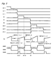
- Fig. 3 is a timing chart showing a timing that data is written to the pixel circuit 10.
- a period from a time t0 to a time t4 corresponds to a period for selecting the pixel circuit 10.
- a process of detecting the threshold voltage of the driving TFT 11 is performed prior to a time t2, a process of writing the corrected data voltage is performed.
- each of the switching TFTs 12 and 13 Prior to the time t0, the potential at each of the scanning line Gi, the control line Wi and the control line Ri is controlled to a low level, each of the switching TFTs 12 and 13 is in a non-conduction state, and the switching TFT 14 is in a conduction state.
- the driving TFT 11 is in the conduction state, and an electric current flows from the power supply wiring line Vp into the organic EL element 15 via the driving TFT 11 and the switching TFT 14, so that the organic EL element 15 emits light.
- each of the switching TFT 12, the switching TFT 13 and the switch 25 is changed to the conduction state while the switching TFT 14 is changed to the non-conduction state.
- the initial voltage Vreset is applied to the data line Sj , and a potential at each of the data line Sj and the node A becomes Vreset.
- the electric current passing through the driving TFT 11 is fed into the node A via the switching TFT 13.
- the switch 25 is changed to the non-conduction state. Also subsequent to the time t1, the electric current passing through the driving TFT 11 is fed into the node A via the switching TFT 13, and a potential at the node A (a potential at the gate terminal of the driving TFT 11) rises during a period that the driving TFT 11 is in the conduction state.
- the switching TFT 12 since the switching TFT 12 is in the conduction state, the potential at the data line Sj is equal to the potential at the node A.
- the potential at the control line SCAN1 is controlled to the low level while the potential at the control line SCAN2 is controlled to the high level. Therefore, each of the switches 21 and 22 is changed to the conduction state while each of the switches 23 and 24 is changed to the non-conduction state.
- the node B is connected to the power supply wiring line Vp and the node C is connected to the data line Sj. Accordingly, the potential at the node B is VDD, and the potential at the node C is equal to the potential at the node A and the potential at the data line Sj.
- each of the switching TFT 13, the switch 21 and the switch 22 is changed to the non-conduction state.
- the potential at the node A is assumed to be (VDD + Vx) (herein, Vx is a negative value, and Vx has an absolute value which is larger than an absolute value of Vth).
- the potential at the node C is also (VDD + Vx). Therefore, when each of the switches 21 and 22 is changed to the non-conduction state at the time t2, the voltage Vx is held at the capacitor 26.
- the potential at the node A rises during the period that the driving TFT 11 is in the conduction state. Accordingly, a satisfactory time allows the potential at the node A to rise until the gate-source voltage of the driving TFT 11 becomes the threshold voltage Vth (negative value) and, finally, reaches (VDD + Vth). At the time t2, the potential (VDD + Vx) at the node A is lower than (VDD + Vth). Moreover, the voltage Vx varies in accordance with the threshold voltage Vth. The absolute value of the voltage Vx becomes larger as the absolute value of the threshold voltage Vth is large.
- each of the switches 23 and 24 is changed to the conduction state.
- the data voltage Vdata outputted from the D/A converter 8 is applied to the node B, and the node C is connected to the data line Sj through the analog buffer 27.
- the switch 24 is in the conduction state, and an input voltage and an output voltage are equal to each other in the analog buffer 27. Therefore, the potential at the data line Sj becomes (Vdata + Vx) as in the case of the node C. Moreover, since the switching TFT 12 is also in the conduction state, the potential at the node A also becomes (Vdata + Vx) as in the case of the data line Sj.
- each of the switching TFT 12, the switch 23 and the switch 24 is changed to the non-conduction state while the switching TFT 14 is changed to the conduction state.
- the gate-source voltage (VDD - Vdata - Vx) of the driving TFT 11 is held at the capacitor 16.
- an ON potential (low level potential) to be given to the control line Ri is determined such that the switching TFT 14 is operated in a linear region.
- a drain-source electric current I EL is obtained from the following equation (1) if a channel length modulation effect is neglected.
- I EL - 1 / 2 ⁇ W / L ⁇ Cox ⁇ ⁇ Vg - VDD - Vth 2
- W/L represents an aspect ratio of the driving TFT 11
- Cox represents a gate capacitance
- ⁇ represents a mobility
- Vg represents a gate terminal potential (i.e., the potential at the node A).
- the electric current I EL expressed by the equation (1) varies in accordance with the threshold voltage Vth.
- the gate terminal potential Vg becomes (Vdata + Vx) ; therefore, the electric current I EL is changed as expressed by the following equation (2).
- I EL - 1 / 2 ⁇ W / L ⁇ Cox ⁇ ⁇ Vdata - VDD + Vx - Vth 2
- the electric current I EL does not depend on the threshold voltage Vth.
- the electric current I EL does not depend on the threshold voltage Vth as long as a difference between the voltage Vx and the threshold voltage Vth is fixed.
- the length of the threshold value correction period (the period from the time t1 to the time t2) and the level of the initial voltage Vreset are determined such that the difference between voltages Vx of two TFTs becomes almost equal to the difference between the threshold voltages Vth of the two TFTs.
- the voltage difference (Vx - Vth) in the equation (2) is almost fixed. Accordingly, an electric current flows into the organic EL element 15 in an amount which depends on the data voltage Vdata irrespective of a value of the threshold voltage Vth, so that the organic EL element 15 emits light at a luminance which depends on the data voltage Vdata.
- the threshold value correction is performed by the threshold value correction circuit 20 provided outside the pixel circuit 10. There is no necessity that the threshold value correction circuit 20 includes a complicated logic circuit and a memory.
- the driving TFT 11 is changed to a diode-connected state.
- a period from a timing that a driving TFT is changed to a diode-connected state to a timing that a gate-source voltage Vgs of the driving TFT satisfactorily approximates a threshold voltage Vth corresponds to a threshold value correction period.
- a period for selecting a pixel circuit is short. Consequently, a voltage Vgs fails to satisfactorily approximate a threshold voltage Vth within the selection period in some instances.
- the parasitic capacitance of the capacitor 26 and the parasitic capacitance of the data line Sj must be charged electrically in order to detect the threshold voltage Vth of the driving TFT 11. Therefore, some contrivance must be made in order to perform the process of detecting the threshold voltage and the process of writing the corrected data voltage within the selection period.
- the constant initial voltage Vreset is applied to the data line Sj by action of the switch 25 in order to detect variations in threshold voltage Vth prior to start of the process of writing the corrected data voltage.
- VDD + Vx the voltage which depends on the threshold voltage Vth of the driving TFT 11 is outputted to the data line Sj. Accordingly, it is possible to suppress variations in correction effect and to improve image quality even when the threshold value correction period is short.
- the initial voltage Vreset is determined based on the length of the threshold value correction period, the accuracy to be required for the threshold value correction, and the like.
- the switching TFT 13 is in the conduction state and the driving TFT 11 is in the diode-connected state
- the following equation (3) is established with regard to an electric current balance in the driving TFT 11.
- k represents a constant
- C represents a sum of a holding capacitance and a signal line capacitance.
- Vgs t 1 k C ⁇ t + 1 Vgs ⁇ 0 - Vth + Vth
- Vgs0 represents an initial value of the voltage Vgs.
- ⁇ Vgs t ⁇ Vth + 1 k C ⁇ t + 1 Vgs ⁇ 0 - Vth - ⁇ Vth - 1 k C ⁇ t + 1 Vgs ⁇ 0 - Vth Accordingly, it is preferable that the initial value Vgs0 of the voltage Vgs is determined such that ⁇ Vgs(t) in the equation (5) satisfactorily approximates ⁇ Vth within a permissible time, and the initial voltage Vreset is obtained in accordance with the initial value Vgs0.
- Fig. 4 shows an example of a temporal change in gate-source voltage Vgs of the diode-connected driving TFT.
- the initial voltage Vgs0 is applied to each of the two TFTs, and the voltages Vgs of the respective TFTs are compared with each other after a lapse of 30 ⁇ s.
- a difference between the two voltages is almost equal to a final value (0.2 V) thereof at this time.
- the difference between the two voltages is different from the final value thereof at this time.
- the threshold value correction period can be made short.
- the absolute value of the initial voltage Vgs0 is made large.
- the absolute value of the initial voltage Vgs0 is made large, power consumption is increased due to electric charge/discharge in the data line Sj and the capacitor 26. Accordingly, it is preferable that the initial voltage Vreset is determined in consideration of a degree and a specification of variations in threshold voltage due to a process.
- the threshold value correction circuit 20 includes the analog buffer 27.
- a capacitance of a data line Sj is not less than several pF in many instances. In such a case, therefore, the analog buffer 27 must be provided.
- use of a voltage follower circuit (a unity gain amplifier) as the analog buffer 27 allows enhancement of a driving capability while suppressing an increase of a circuit scale as much as possible.
- the analog buffer 27 is not formed on the display panel, but is incorporated in a peripheral IC provided outside the display panel.
- the circuit incorporated in the peripheral IC is formed with a transistor made of polycrystalline silicon. Accordingly, when the analog buffer 27 is incorporated in the peripheral IC, the variations in characteristic can be made considerably small.
- a buffer having an offset cancel function may be used as the analog buffer 27.
- a differential amplifier 31 has a positive-side input terminal connected to an input terminal of the buffer, a negative-side input terminal connected to a first electrode of a capacitor 32, and an output terminal connected to an output terminal of the buffer.
- a switch 33 is provided between a second electrode of the capacitor 32 and an input terminal of the buffer.
- a switch 34 is provided between the negative-side input terminal and the output terminal of the differential amplifier 31.
- a switch 35 is provided between the second electrode of the capacitor 32 and the output terminal of the differential amplifier 31.
- Each of the switches 33 and 34 is controlled by a control signal SC_A while the switch 35 is controlled by a control signal SC_B.
- Each of the control signals SC_A and SC_B exclusively becomes a level at which the switch is changed to a conduction state (corresponding to a high level herein), as shown in Fig. 5B .
- each of the switches 33 and 34 becomes the conduction state while the switch 35 becomes a non-conduction state.
- an offset voltage Voff of the differential amplifier 31 appears between the positive-side input terminal and the negative-side input terminal of the differential amplifier 31. The offset voltage Voff is held by the capacitor 32.
- each of the switches 33 and 34 becomes the non-conduction state while the switch 35 becomes the conduction state.
- a negative-side input voltage of the differential amplifier 31 varies by the offset voltage Voff
- an output voltage of the differential amplifier 31 i.e. , an output voltage of the buffer
- use of the buffer shown in Fig. 5A allows cancellation of the offset voltage of the differential amplifier 31.
- the buffer having the offset cancel function may be incorporated in the peripheral IC provided outside the display panel.
- the voltage (VDD + Vx) which depends on the threshold voltage Vth of the driving TFT 11 can be read from the pixel circuit 10 selected by the gate driver circuit 3 and the voltage (Vdata + Vx), which is obtained by adding the correction voltage Vx (the voltage corresponding to the threshold voltage Vth) to the data voltage Vdata, can be applied to the gate terminal of the driving TFT 11.
- VDD + Vx the voltage which depends on the threshold voltage Vth of the driving TFT 11
- Vdata + Vx which is obtained by adding the correction voltage Vx (the voltage corresponding to the threshold voltage Vth) to the data voltage Vdata
- the threshold value correction circuit 20 is provided outside the pixel circuit and the threshold voltage is detected by use of the data line Sj, leading to reduction in scale and area of the pixel circuit 10. Further, the threshold voltage is detected as a voltage signal, so that a current-voltage conversion element becomes unnecessary unlike a case where an electric current signal is fed back. Therefore, variations in correction effect can be suppressed.
- the correction voltage Vx corresponding to the threshold voltage is added as it is to the data voltage Vdata, so that the threshold value correction can be performed with high accuracy.
- a desired voltage is applied to the gate terminal of the driving TFT 11 through no coupling capacitance. Therefore, an amplitude of the data voltage Vdata can be utilized effectively, leading to reduction in power consumption.
- the display device may include a pixel circuit shown in Fig. 6A or 6B in place of the pixel circuit 10.
- the pixel circuit 17 shown in Fig. 6A is different from the pixel circuit 10 in a point that a switching TFT 14 is connected to a scanning line Gi such that the scanning line Gi and a control line Ri are shared. In the pixel circuit 17, each of switching TFTs 12 and 14 becomes a conduction state exclusively.
- the pixel circuit 18 shown in Fig. 6B is different from the pixel circuit 10 in a point that a switching TFT 13 is connected to a control line Ri such that the control line Ri and a control line Wi are shared. In the pixel circuit 18, each of switching TFTs 13 and 14 becomes a conduction state exclusively.
- Each of the display devices according to these modified examples operates as in the display device including the pixel circuit 10 and has advantageous effects similar to those of the display device including the pixel circuit 10.
- the switching TFTs 12 to 14 share a wiring line to be connected to control terminals thereof, so that the number of wiring lines is reduced from three to two. Further, an aperture ratio of a pixel is made higher. Thus, a screen can be made brighter.
- Fig. 7 is a circuit diagram showing a pixel circuit and a threshold value correction circuit each included in the display device according to the second embodiment of the present invention.
- the pixel circuit 40 and the threshold value correction circuit 50 in Fig. 7 correspond to the pixel circuit Aij and the threshold value correction circuit 9 in Fig. 1 .
- the pixel circuit 40 includes a driving TFT 41, switching TFTs 42 to 44, an organic EL element 45 and a capacitor 46.
- the driving TFT 41 is of an enhancement N-channel type, and each of the switching TFTs 42 to 44 is of an N-channel type.
- the organic EL element 45, the switching TFT 44 and the driving TFT 41 are provided in series between a power supply wiring line Vp and a common cathode Vcom sequentially from a side of the power supply wiring line Vp.
- the switching TFT 42 is provided between a gate terminal of the driving TFT 41 and a data line Sj.
- the switching TFT 43 is provided between the gate terminal and a drain terminal of the driving TFT 41, and the capacitor 46 is provided between the gate terminal of the driving TFT 41 and the common cathode Vcom.
- the switching TFT 42 has a gate terminal connected to a scanning line Gi
- the switching TFT 43 has a gate terminal connected to a control line Wi
- the switching TFT 44 has a gate terminal connected to a control line Ri.
- the threshold value correction circuit 50 has a structure which is equal to that of the threshold value correction circuit 20 according to the first embodiment. In the threshold value correction circuit 50, however, a switch 22 is provided between a node B and the common cathode Vcom. The threshold value correction circuit 50 is equal to the threshold value correction circuit 20 except the point described above.
- Fig. 8 is a timing chart showing a timing that data is written to the pixel circuit 40.
- the display device according to this embodiment operates as in the display device according to the first embodiment, and has advantageous effects similar to those of the display device according to the first embodiment.
- a driving TFT of an N-channel type typically, when a voltage obtained by addition of an absolute value of a threshold voltage is applied to a gate terminal, variations in threshold voltage can be compensated.
- this embodiment can adopt the modified example that the switching TFTs 42 to 44 share a wiring line to be connected to control terminals thereof.
- the pixel circuit 40 in which each of the driving TFT 41 and the switching TFT 42, 43 and 44 is of an N-channel type, can be applied to a display panel using amorphous silicon.
- the analog buffer 27 is provided for each data line Sj.
- a pitch between the sub pixels is about 42 ⁇ m.
- the capacitor 26 that holds the correction voltage Vx which depends on the threshold voltage of the driving TFT can be arranged at this pitch, but the high-performance analog buffer 27 can not be arranged at this pitch in some instances. In the third embodiment, therefore, description will be given of the display device in which the number of analog buffers 27 is reduced.
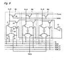
- Fig. 9 is a circuit diagram showing a threshold value correction circuit included in the display device according to the third embodiment of the present invention.
- the threshold value correction circuits 60r, 60g and 60b in Fig. 9 correspond to the threshold value correction circuit 9 in Fig. 1 .
- data lines Sj_R, Sj_G and Sj_B in Fig. 9 correspond to the data line Sj in Fig. 1 .
- an analog buffer 27 is provided in correspondence with the three data lines Sj_R, Sj_G and Sj_B.
- the threshold value correction circuit 60r is different from the threshold value correction circuit 20 ( Fig. 2 ) according to the first embodiment in a point that a function of sharing the analog buffer 27 is added thereto.
- a switch 61 is provided between a first electrode.of a capacitor 26 (an electrode shown at an upper side of Fig. 9 ) and an input terminal of the analog buffer 27.
- switches 23, 24 and 61 have gate terminals connected to a control line SCAN1_R.
- Each of the threshold value correction circuits 60g and 60b is similar in configuration to the threshold value correction circuit 60r.
- Fig. 10 is a timing chart showing a timing that data is written to a pixel circuit in the display device according to this embodiment.
- a period from a time t0 to a time t4 corresponds to a period for selecting the three pixel circuits.
- a process of detecting threshold voltages of driving TFTs of the three pixel circuits in parallel is performed prior to a time t2.
- the display device includes the pixel circuit 18 shown in Fig. 6B ; however, a type of the pixel circuit may be arbitrary.
- a potential at each of the scanning line Gi and a control line Ri is controlled to a low level.
- a potential at each of the scanning line Gi, the control line Ri and a control line SCAN3 is changed to a high level, a potential at each of the data lines Sj_R, Sj_G and Sj_B as well as a potential at each of the gate terminals of the driving TFTs of the three pixel circuits become Vreset.
- the potentials at the gate terminals of the driving TFTs of the three pixel circuits are assumed to be (VDD+Vx_r), (VDD+Vx_g) and (VDD+Vx_b), respectively (Vx_r, Vx_g, Vx_r: negative values).
- Vx_r, Vx_g, Vx_r: negative values the potential at each of the control line Ri and the control line SCAN2 is changed to the low level.
- the potential at each of the control lines SCAN1_R, SCAN1_G and SCAN1_B becomes the high level by a predetermined time and, in synchronization with this, a data voltage Vdata outputted from a D/A converter 8 is changed to Vd_r, Vd_g and Vd_b.
- Vd_r + Vx_r the potential at the gate terminal of the driving TFT of the pixel circuit connected to the data line Sj_R becomes (Vd_r + Vx_r) .
- the potential at the gate terminal of the driving TFT of the pixel circuit connected to the data line Sj_G becomes (Vd_g + Vx_g) .
- the potential at the gate terminal of the driving TFT of the pixel circuit connected to the data line Sj_B becomes (Vd_b + Vx_b).
- the potentials at the gate terminals of the driving TFTs of the three pixel circuits are maintained at (Vd_r + Vx_r), (Vd_g + Vx_g) and (Vd_b + Vx_b), respectively.
- amounts of electric currents flowing through the respective driving TFTs increase/decrease in accordance with these potentials.
- the electric current amount is the same as long as the data voltage is the same even when the threshold voltage is different. Accordingly, an electric current flows into an organic EL element of each pixel circuit in an amount which depends on the data voltage Vdata irrespective of a value of the threshold voltage, so that the organic EL element emits light at a luminance which depends on the data voltage Vdata.
- the analog buffer is provided in correspondence with the three data lines Sj_R, Sj_G and Sj_B.
- the analog buffer may be provided in correspondence with "p" (p: an arbitrary integer of two or more) data lines.
- the display device realizes a display panel with high definition in such a manner that the analog buffer having a large circuit scale is not arranged for each data line, but is arranged for the plurality of data lines.
- the pixel circuit includes the organic EL element as an electro-optical element.
- the pixel circuit may include an electro-optical element of an electric current driving type other than the organic EL element (e.g. , a semiconductor LED, a light emitting part of an FED).
- the pixel circuit includes, as a drive element of the electro-optical element, the TFT which is a MOS transistor (including a silicon gate MOS structure) formed on an insulating substrate such as a glass substrate.
- the pixel circuit may include an arbitrary voltage controlling element having a threshold voltage (i.e., an element that changes an output current in accordance with a control voltage applied to a control terminal thereof and interrupts the output current when the control voltage becomes not less than or not more than a predetermined value).
- the pixel circuit may include, as a drive element, a typical insulating gate-type field effect transistor including a MOS transistor formed on a semiconductor substrate.
- the switching TFT 12 is changed to the conduction state and, almost simultaneously, the switching TFT 13 is changed to the conduction state while the switching TFT 14 is changed to the non-conduction state.
- the switching TFT 13 may be changed to the conduction state while the switching TFT 14 may be changed to the non-conduction state.
- the present invention is not limited to the foregoing embodiments and may be modified variously. Moreover, an embodiment obtained by appropriately combining the technical means disclosed in the different embodiments with one another is also involved in the technical scope of the present invention.
- the display device according to the present invention has an advantageous effect of efficiently utilizing an amplitude of a data voltage and performing threshold value correction with high accuracy, without increasing a scale of a pixel circuit. Therefore, the display device according to the present invention can be used as a display device for various electronic appliances.
Claims (11)
- Anzeigeeinrichtung (1) vom Typ mit Ansteuerung durch elektrischen Strom,
mit:einer Mehrzahl von Pixelschaltungen (10), die in Korrespondenz mit Kreuzungspunkten einer Mehrzahl von Abtastleitungen (Gi) und einer Mehrzahl von Datenleitungen (Sj) angeordnet sind, wobei jede Pixelschaltung (10) ein elektrooptisches Element (15) und ein Steuerelement (11) mit einem Steueranschluss aufweist, welcher mit einer Datenleitung (Sj) über ein erstes Schaltelement (12) verbunden ist,einer Abtastsignalausgabeschaltung (3), welche eine Schreibzielpixelschaltung (10) über Verwendung einer Abtastleitung (Gi) auswählt, wobei die Abtastsignalausgabeschaltung (3) eine Steuerung derart ausübt, dass eine Spannung am Steueranschluss des Steuerelements (11) sich einer Schwellwertspannung (Vth) des Steuerelements (11) in einer Schwellwertkorrekturzeitspanne nähert, und wobei die Abtastsignalausgabeschaltung (3) eine Steuerung derart ausübt, dass die Schreibzielpixelschaltung (10) an die Datenleitung eine Korrekturspannung (Vx) ausgibt, welche eine Spannung am Steueranschluss am Ende der Schwellwertkorrekturzeitspanne ist, wobei die Korrekturspannung (Vx) von der Schwellwertspannung (Vth) abhängt, undeiner Anzeigesignalausgabeschaltung (4), welche an die Datenleitung (Sj) in einer Zeitspanne, welche der Schwellwertkorrekturzeitspanne folgt, eine Spannung anlegt, die erhalten wird durch Addieren oder Subtrahieren der Korrekturspannung (Vx) zu oder von einer Datenspannung (Vdata), welche zu Anzeigedaten korrespondiert, und zwar auf der Grundlage der an die Datenleitung (Sj) ausgegebenen Spannung,dadurch gekennzeichnet,dass die Anzeigeeinrichtung derart ausgebildet ist, dass die Schwellwertkorrekturzeitspanne endet, bevor die Spannung am Steueranschluss die Schwellwertspannung (Vth) erreicht. - Anzeigeeinrichtung nach Anspruch 1,
wobei
das elektrooptische Element (15) und das Steuerelement (11) zwischen zwei Stromversorgungsleitungen in der Pixelschaltung (10) in Serie ausgebildet sind und
die Pixelschaltung (10) des Weiteren aufweist:ein erstes Schaltelement (12), welches mit einem Steueranschluss des Steuerelements und der Datenleitung verbunden ist,ein zweites Schaltelement (13), welches zwischen dem Steueranschluss und einem leitenden Anschluss des Steuerelements ausgebildet ist,ein drittes Schaltelement (14), welches zusammen mit dem elektrooptischen Element (15) und dem Steuerelement (11) zwischen den Stromversorgungsleitungen in Serie ausgebildet ist, undeine Kapazität (16) mit einem Ende, welches mit dem Steueranschluss des Steuerelements verbunden ist. - Anzeigeeinrichtung nach Anspruch 2,
wobei
die Abtastsignalausgabeschaltung (3) die Schreibzielpixelschaltung (10) derart steuert, dass die ersten und zweiten Schaltelemente (12, 13) in einen Leitungszustand gesetzt werden, dass das dritte Schaltelement (14) in der Schwellwertkorrekturzeitspanne in einen Nichtleitungszustand gesetzt wird, dass dann das zweite Schaltelement (13) zum Nichtleitungszustand gewechselt wird, dass dann das erste Schaltelement (12) zum Nichtleitungszustand gewechselt wird und das dritte Schaltelement (14) zum Leitungszustand gewechselt wird, und
die Anzeigesignalausgabeschaltung (4) an die Datenleitung (Sj) die Spannung anlegt, die erhalten wird durch Addieren oder Subtrahieren der Korrekturspannung (Vx) zu oder von der Datenspannung (Vdata), nachdem das zweite Schaltelement (13) zum Nichtleitungszustand gewechselt wurde, und zwar auf der Grundlage einer Spannung der Datenleitung (Sj), falls das zweite Schaltelement (13) sich im Leitungszustand befindet. - Anzeigeeinrichtung nach Anspruch 2,
wobei
das Steuerelement (11) und die ersten bis dritten Schaltelemente (12, 13, 14) Dünnschichttransistoren sind,
eines der ersten und dritten Schaltelemente (12, 14) vom P-Kanaltyp und das andere Schaltelement (14, 12) vom N-Kanaltyp ist und
die ersten und dritten Schaltelemente (12, 14) Steueranschlüsse aufweisen, die mit einer gemeinsamen Anschlussleitung (Gi) verbunden sind. - Anzeigeeinrichtung nach Anspruch 2,
wobei
das Steuerelement (11) und die ersten bis dritten Schaltelemente (12, 13, 14) Dünnschichttransistoren sind,
eines der zweiten und dritten Schaltelemente (13, 14) von einem P-Kanaltyp und das andere Schaltelement (14, 13) vom N-Kanaltyp ist und
die zweiten und dritten Schaltelemente (13, 14) Steueranschlüsse aufweisen, die mit einer gemeinsamen Anschlussleitung (Ri) verbunden sind. - Anzeigeeinrichtung nach Anspruch 2,
wobei
das Steuerelement (11) ein Transistor vom Anreicherungs-P-Kanaltyp ist und
die Schreibzielpixelschaltung (10), die von der Abtastsignalausgabeschaltung (3) ausgewählt wurde, an die Datenleitung (Sj) eine Spannung ausgibt, die erhalten wird durch Subtrahieren eines Absolutwertes der angelegten Spannung am Ende der Schwellwertkorrekturzeitspanne von einer höheren der Spannungen der Stromversorgungsleitungen. - Anzeigeeinrichtung nach Anspruch 2,
wobei
das Steuerelement (11) ein Transistor vom Anreicherungs-N-Kanaltyp ist und
wobei die Schreibzielpixelschaltung (10), die von der Abtastsignalausgabeschaltung (3) ausgewählt wurde, an die Datenleitung (Sj) eine Spannung ausgibt, die erhalten wird durch Addieren eines Absolutwertes der angelegten Spannung am Ende der Schwellwertkorrekturzeitspanne zu einer niedrigeren der Spannungen der Stromversorgungsleitungen. - Anzeigeeinrichtung nach Anspruch 2,
wobei die Anzeigesignalausgabeschaltung (4) eine vorbestimmte konstante Spannung an die Datenleitung in einem Teil einer Leitungszeitspanne des ersten Schaltelements anlegt. - Anzeigeeinrichtung nach Anspruch 1,
wobei
die Anzeigesignalausgabeschaltung (4) eine Mehrzahl von Analogpuffern (27) aufweist sowie eine Mehrzahl von Korrekturkapazitäten (26) und eine Mehrzahl von Wechselschaltungen, die für jede Datenleitung vorgesehen sind, und
die Wechselschaltung zwischen einem Zustand, bei welchem eine Elektrode der Korrekturkapazität (26) mit der Datenleitung (Sj) verbunden ist und die andere Elektrode davon mit einer vorbestimmten konstanten Spannung (Vp) beaufschlagt ist, und einem Zustand wechselt, bei welchem eine Elektrode der Korrekturkapazität (26) über den Analogpuffer (27) mit der Datenleitung (Sj) verbunden ist und die andere Elektrode davon mit der Datenspannung (Vdata) beaufschlagt ist. - Anzeigeeinrichtung nach Anspruch 9,
wobei der Analogpuffer (27) mit einer Mehrzahl von Datenleitungen (Sj) ausgebildet ist. - Verfahren zum Steuern einer Anzeigeeinrichtung (1) mit einer Mehrzahl von Pixelschaltungen (16), die in Korrespondenz mit Kreuzungspunkten einer Mehrzahl von Abtastleitungen (Gi) und einer Mehrzahl von Datenleitungen (Sj) angeordnet sind, wobei jede Pixelschaltung (10) ein elektrooptisches Element (15) und ein Steuerelement (11) aufweist mit einem Steueranschluss, der über ein Schaltelement (12) mit der Datenleitung (Sj) verbunden ist,
wobei das Verfahren die Schritte aufweist:Auswählen einer Schreibzielpixelschaltung (10) über Verwendung der Abtastleitung (Gi) und Ausüben einer Steuerung derart, dass eine Spannung am Steueranschluss des Steuerelements (11) sich einer Schwellwertspannung (Vth) des Steuerelements (11) in einer Schwellwertkorrekturzeitspanne annähert und die ausgewählte Schreibzielpixelschaltung (10) an die Datenleitung (Sj) eine Korrekturspannung (Vx) ausgibt, welche eine Spannung am Steueranschluss am Ende der Schwellwertkorrekturzeitspanne ist, und - in einer Zeitspanne, welche der Schwellwertkorrekturzeitspanne folgt,Anlegen einer Spannung, die erhalten wird durch Addieren oder Subtrahieren der Korrekturspannung (Vx) zu oder von einer Datenspannung, die mit den Anzeigedaten korrespondiert, an die Datenleitung (Sj), und zwar auf der Grundlage der an die Datenleitung (Sj) ausgegebenen Spannung,dadurch gekennzeichnet,dass die Schwellwertkorrekturzeitspanne endet, bevor die Spannung am Steueranschluss die Schwellwertspannung (Vth) erreicht.
Applications Claiming Priority (2)
| Application Number | Priority Date | Filing Date | Title |
|---|---|---|---|
| JP2007058021 | 2007-03-08 | ||
| EP07828924A EP2093748B1 (de) | 2007-03-08 | 2007-10-01 | Anzeigeanordnung und verfahren zu ihrer ansteuerung |
Related Parent Applications (1)
| Application Number | Title | Priority Date | Filing Date |
|---|---|---|---|
| EP07828924.6 Division | 2007-10-01 |
Publications (2)
| Publication Number | Publication Date |
|---|---|
| EP2369571A1 EP2369571A1 (de) | 2011-09-28 |
| EP2369571B1 true EP2369571B1 (de) | 2013-04-03 |
Family
ID=39737925
Family Applications (2)
| Application Number | Title | Priority Date | Filing Date |
|---|---|---|---|
| EP07828924A Not-in-force EP2093748B1 (de) | 2007-03-08 | 2007-10-01 | Anzeigeanordnung und verfahren zu ihrer ansteuerung |
| EP11003018A Not-in-force EP2369571B1 (de) | 2007-03-08 | 2007-10-01 | Anzeigevorrichtung und Ansteuerungsverfahren dafür |
Family Applications Before (1)
| Application Number | Title | Priority Date | Filing Date |
|---|---|---|---|
| EP07828924A Not-in-force EP2093748B1 (de) | 2007-03-08 | 2007-10-01 | Anzeigeanordnung und verfahren zu ihrer ansteuerung |
Country Status (5)
| Country | Link |
|---|---|
| US (1) | US8847939B2 (de) |
| EP (2) | EP2093748B1 (de) |
| JP (1) | JP5171807B2 (de) |
| CN (2) | CN102097055A (de) |
| WO (1) | WO2008108024A1 (de) |
Families Citing this family (89)
| Publication number | Priority date | Publication date | Assignee | Title |
|---|---|---|---|---|
| CA2443206A1 (en) | 2003-09-23 | 2005-03-23 | Ignis Innovation Inc. | Amoled display backplanes - pixel driver circuits, array architecture, and external compensation |
| US7608861B2 (en) * | 2004-06-24 | 2009-10-27 | Canon Kabushiki Kaisha | Active matrix type display having two transistors of opposite conductivity acting as a single switch for the driving transistor of a display element |
| CA2490858A1 (en) | 2004-12-07 | 2006-06-07 | Ignis Innovation Inc. | Driving method for compensated voltage-programming of amoled displays |
| US10013907B2 (en) | 2004-12-15 | 2018-07-03 | Ignis Innovation Inc. | Method and system for programming, calibrating and/or compensating, and driving an LED display |
| US8576217B2 (en) | 2011-05-20 | 2013-11-05 | Ignis Innovation Inc. | System and methods for extraction of threshold and mobility parameters in AMOLED displays |
| US9799246B2 (en) | 2011-05-20 | 2017-10-24 | Ignis Innovation Inc. | System and methods for extraction of threshold and mobility parameters in AMOLED displays |
| US7852298B2 (en) | 2005-06-08 | 2010-12-14 | Ignis Innovation Inc. | Method and system for driving a light emitting device display |
| US9489891B2 (en) | 2006-01-09 | 2016-11-08 | Ignis Innovation Inc. | Method and system for driving an active matrix display circuit |
| WO2007118332A1 (en) | 2006-04-19 | 2007-10-25 | Ignis Innovation Inc. | Stable driving scheme for active matrix displays |
| CA2556961A1 (en) | 2006-08-15 | 2008-02-15 | Ignis Innovation Inc. | Oled compensation technique based on oled capacitance |
| JP5495510B2 (ja) * | 2007-06-19 | 2014-05-21 | キヤノン株式会社 | 表示装置及びそれを用いた電子機器 |
| JP5217500B2 (ja) * | 2008-02-28 | 2013-06-19 | ソニー株式会社 | El表示パネルモジュール、el表示パネル、集積回路装置、電子機器及び駆動制御方法 |
| JP2009204992A (ja) * | 2008-02-28 | 2009-09-10 | Sony Corp | El表示パネル、電子機器及びel表示パネルの駆動方法 |
| CN102113043B (zh) * | 2008-09-10 | 2014-03-05 | 夏普株式会社 | 显示装置及其驱动方法 |
| US9370075B2 (en) | 2008-12-09 | 2016-06-14 | Ignis Innovation Inc. | System and method for fast compensation programming of pixels in a display |
| KR101634286B1 (ko) * | 2009-01-23 | 2016-07-11 | 삼성디스플레이 주식회사 | 표시 장치 및 그 구동 방법 |
| US9384698B2 (en) | 2009-11-30 | 2016-07-05 | Ignis Innovation Inc. | System and methods for aging compensation in AMOLED displays |
| US9311859B2 (en) | 2009-11-30 | 2016-04-12 | Ignis Innovation Inc. | Resetting cycle for aging compensation in AMOLED displays |
| US10319307B2 (en) | 2009-06-16 | 2019-06-11 | Ignis Innovation Inc. | Display system with compensation techniques and/or shared level resources |
| KR101082283B1 (ko) * | 2009-09-02 | 2011-11-09 | 삼성모바일디스플레이주식회사 | 유기전계발광 표시장치 및 그의 구동방법 |
| US20140313111A1 (en) | 2010-02-04 | 2014-10-23 | Ignis Innovation Inc. | System and methods for extracting correlation curves for an organic light emitting device |
| US9881532B2 (en) | 2010-02-04 | 2018-01-30 | Ignis Innovation Inc. | System and method for extracting correlation curves for an organic light emitting device |
| CA2692097A1 (en) | 2010-02-04 | 2011-08-04 | Ignis Innovation Inc. | Extracting correlation curves for light emitting device |
| US10089921B2 (en) | 2010-02-04 | 2018-10-02 | Ignis Innovation Inc. | System and methods for extracting correlation curves for an organic light emitting device |
| US8907991B2 (en) | 2010-12-02 | 2014-12-09 | Ignis Innovation Inc. | System and methods for thermal compensation in AMOLED displays |
| US9886899B2 (en) * | 2011-05-17 | 2018-02-06 | Ignis Innovation Inc. | Pixel Circuits for AMOLED displays |
| US9351368B2 (en) * | 2013-03-08 | 2016-05-24 | Ignis Innovation Inc. | Pixel circuits for AMOLED displays |
| US20140368491A1 (en) * | 2013-03-08 | 2014-12-18 | Ignis Innovation Inc. | Pixel circuits for amoled displays |
| US9530349B2 (en) | 2011-05-20 | 2016-12-27 | Ignis Innovations Inc. | Charged-based compensation and parameter extraction in AMOLED displays |
| US9466240B2 (en) | 2011-05-26 | 2016-10-11 | Ignis Innovation Inc. | Adaptive feedback system for compensating for aging pixel areas with enhanced estimation speed |
| CN106910464B (zh) | 2011-05-27 | 2020-04-24 | 伊格尼斯创新公司 | 补偿显示器阵列中像素的系统和驱动发光器件的像素电路 |
| CN103597534B (zh) | 2011-05-28 | 2017-02-15 | 伊格尼斯创新公司 | 用于快速补偿显示器中的像素的编程的系统和方法 |
| US8710505B2 (en) * | 2011-08-05 | 2014-04-29 | Semiconductor Energy Laboratory Co., Ltd. | Semiconductor device |
| WO2013073466A1 (ja) * | 2011-11-17 | 2013-05-23 | シャープ株式会社 | 表示装置およびその駆動方法 |
| US9466239B2 (en) | 2011-11-17 | 2016-10-11 | Sharp Kabushiki Kaisha | Current drive type display device and drive method thereof |
| KR101938880B1 (ko) * | 2011-11-18 | 2019-01-16 | 엘지디스플레이 주식회사 | 유기발광다이오드 표시장치 |
| US9324268B2 (en) | 2013-03-15 | 2016-04-26 | Ignis Innovation Inc. | Amoled displays with multiple readout circuits |
| US10089924B2 (en) | 2011-11-29 | 2018-10-02 | Ignis Innovation Inc. | Structural and low-frequency non-uniformity compensation |
| JP6124573B2 (ja) | 2011-12-20 | 2017-05-10 | キヤノン株式会社 | 表示装置 |
| US8937632B2 (en) | 2012-02-03 | 2015-01-20 | Ignis Innovation Inc. | Driving system for active-matrix displays |
| JP5887973B2 (ja) * | 2012-02-13 | 2016-03-16 | セイコーエプソン株式会社 | 電気光学装置、電気光学装置の駆動方法および電子機器 |
| JP6141048B2 (ja) * | 2012-04-23 | 2017-06-07 | キヤノン株式会社 | 発光素子の駆動装置および表示装置 |
| JP6111531B2 (ja) * | 2012-04-25 | 2017-04-12 | セイコーエプソン株式会社 | 電気光学装置、電気光学装置の駆動方法および電子機器 |
| JP6015095B2 (ja) | 2012-04-25 | 2016-10-26 | セイコーエプソン株式会社 | 電気光学装置および電子機器 |
| US9747834B2 (en) | 2012-05-11 | 2017-08-29 | Ignis Innovation Inc. | Pixel circuits including feedback capacitors and reset capacitors, and display systems therefore |
| US8922544B2 (en) | 2012-05-23 | 2014-12-30 | Ignis Innovation Inc. | Display systems with compensation for line propagation delay |
| KR20140013482A (ko) * | 2012-07-24 | 2014-02-05 | 삼성디스플레이 주식회사 | 터치 스크린 패널 일체형 표시장치 |
| WO2014021150A1 (ja) | 2012-07-31 | 2014-02-06 | シャープ株式会社 | 表示装置およびその駆動方法 |
| US9786223B2 (en) | 2012-12-11 | 2017-10-10 | Ignis Innovation Inc. | Pixel circuits for AMOLED displays |
| US9336717B2 (en) | 2012-12-11 | 2016-05-10 | Ignis Innovation Inc. | Pixel circuits for AMOLED displays |
| KR102057286B1 (ko) * | 2013-02-21 | 2019-12-19 | 삼성디스플레이 주식회사 | 유기전계발광 표시장치 |
| US9721505B2 (en) | 2013-03-08 | 2017-08-01 | Ignis Innovation Inc. | Pixel circuits for AMOLED displays |
| CA2894717A1 (en) | 2015-06-19 | 2016-12-19 | Ignis Innovation Inc. | Optoelectronic device characterization in array with shared sense line |
| EP3043338A1 (de) | 2013-03-14 | 2016-07-13 | Ignis Innovation Inc. | Neuinterpolation mit kantendetektion zur extraktion eines alterungsmusters für amoled-anzeigen |
| KR20140120085A (ko) | 2013-04-02 | 2014-10-13 | 삼성디스플레이 주식회사 | 표시 패널 구동부, 이를 이용한 표시 패널 구동 방법 및 이를 포함하는 표시 장치 |
| JP6138244B2 (ja) | 2013-04-23 | 2017-05-31 | シャープ株式会社 | 表示装置およびその駆動電流検出方法 |
| KR20140132504A (ko) * | 2013-05-08 | 2014-11-18 | 삼성디스플레이 주식회사 | 화소 및 이를 이용한 유기전계발광 표시장치 |
| WO2014203810A1 (ja) * | 2013-06-20 | 2014-12-24 | シャープ株式会社 | 表示装置およびその駆動方法 |
| US9761170B2 (en) | 2013-12-06 | 2017-09-12 | Ignis Innovation Inc. | Correction for localized phenomena in an image array |
| US9842545B2 (en) * | 2013-12-20 | 2017-12-12 | Sharp Kabushiki Kaisha | Display device and method for driving same |
| US9502653B2 (en) | 2013-12-25 | 2016-11-22 | Ignis Innovation Inc. | Electrode contacts |
| JP6535441B2 (ja) | 2014-08-06 | 2019-06-26 | セイコーエプソン株式会社 | 電気光学装置、電子機器、及び電気光学装置の駆動方法 |
| CA2873476A1 (en) | 2014-12-08 | 2016-06-08 | Ignis Innovation Inc. | Smart-pixel display architecture |
| CA2879462A1 (en) | 2015-01-23 | 2016-07-23 | Ignis Innovation Inc. | Compensation for color variation in emissive devices |
| CA2886862A1 (en) | 2015-04-01 | 2016-10-01 | Ignis Innovation Inc. | Adjusting display brightness for avoiding overheating and/or accelerated aging |
| CA2889870A1 (en) | 2015-05-04 | 2016-11-04 | Ignis Innovation Inc. | Optical feedback system |
| CA2892714A1 (en) | 2015-05-27 | 2016-11-27 | Ignis Innovation Inc | Memory bandwidth reduction in compensation system |
| CA2898282A1 (en) | 2015-07-24 | 2017-01-24 | Ignis Innovation Inc. | Hybrid calibration of current sources for current biased voltage progra mmed (cbvp) displays |
| US10373554B2 (en) | 2015-07-24 | 2019-08-06 | Ignis Innovation Inc. | Pixels and reference circuits and timing techniques |
| US10657895B2 (en) | 2015-07-24 | 2020-05-19 | Ignis Innovation Inc. | Pixels and reference circuits and timing techniques |
| CA2900170A1 (en) | 2015-08-07 | 2017-02-07 | Gholamreza Chaji | Calibration of pixel based on improved reference values |
| US9516249B1 (en) * | 2015-09-03 | 2016-12-06 | Omnivision Technologies, Inc. | Pixel control signal driver |
| CA2908285A1 (en) | 2015-10-14 | 2017-04-14 | Ignis Innovation Inc. | Driver with multiple color pixel structure |
| CN105321453A (zh) * | 2015-12-01 | 2016-02-10 | 武汉华星光电技术有限公司 | 显示面板以及显示装置 |
| JP6733361B2 (ja) * | 2016-06-28 | 2020-07-29 | セイコーエプソン株式会社 | 表示装置及び電子機器 |
| KR102650339B1 (ko) * | 2016-12-27 | 2024-03-21 | 엘지디스플레이 주식회사 | 전계 발광 표시 장치 |
| JP6520981B2 (ja) * | 2017-04-19 | 2019-05-29 | セイコーエプソン株式会社 | 表示装置及び電子機器 |
| US10424247B2 (en) * | 2017-04-28 | 2019-09-24 | Shenzhen China Star Optoelectronics Semiconductor Display Technology Co., Ltd | AMOLED driving circuit and AMOLED display device |
| CN109427308B (zh) * | 2017-08-22 | 2021-01-22 | 奇景光电股份有限公司 | 补偿像素电压的显示面板驱动装置与方法 |
| WO2019112683A1 (en) * | 2017-12-06 | 2019-06-13 | Apple Inc. | Method and apparatus for mitigating lateral leakage current on organic light-emitting diode displays |
| CN107833559B (zh) * | 2017-12-08 | 2023-11-28 | 合肥京东方光电科技有限公司 | 像素驱动电路、有机发光显示面板及像素驱动方法 |
| CN108766354A (zh) * | 2018-05-30 | 2018-11-06 | 昆山国显光电有限公司 | 显示面板及其驱动方法、显示装置 |
| WO2020056676A1 (en) * | 2018-09-20 | 2020-03-26 | Boe Technology Group Co., Ltd. | A pixel circuit with a time-shared signal line, a pixel compensation method, and a display apparatus |
| US11217161B2 (en) * | 2018-09-20 | 2022-01-04 | Boe Technology Group Co., Ltd. | Display-driving circuit, method, and display apparatus |
| CN109410837B (zh) * | 2018-12-17 | 2020-12-04 | 深圳市华星光电半导体显示技术有限公司 | 一种oled驱动芯片及其驱动方法 |
| CN110767158B (zh) | 2019-03-29 | 2020-10-27 | 昆山国显光电有限公司 | 显示装置及其显示面板、显示面板的像素驱动电路 |
| JP6852749B2 (ja) * | 2019-04-25 | 2021-03-31 | セイコーエプソン株式会社 | 表示装置及び電子機器 |
| CN110689837B (zh) * | 2019-10-29 | 2023-11-28 | 深圳市华星光电半导体显示技术有限公司 | 像素驱动电路以及显示面板 |
| CN111653240A (zh) * | 2020-06-30 | 2020-09-11 | 京东方科技集团股份有限公司 | 像素驱动电路及其驱动方法、显示面板及其驱动方法 |
Family Cites Families (21)
| Publication number | Priority date | Publication date | Assignee | Title |
|---|---|---|---|---|
| JP2970545B2 (ja) | 1996-07-30 | 1999-11-02 | 日本電気株式会社 | モノリシックレンズの製造方法 |
| US6229506B1 (en) * | 1997-04-23 | 2001-05-08 | Sarnoff Corporation | Active matrix light emitting diode pixel structure and concomitant method |
| KR20050084509A (ko) | 1997-04-23 | 2005-08-26 | 사르노프 코포레이션 | 능동 매트릭스 발광 다이오드 화소 구조물 및 이를동작시키는 방법 |
| KR100370286B1 (ko) * | 2000-12-29 | 2003-01-29 | 삼성에스디아이 주식회사 | 전압구동 유기발광소자의 픽셀회로 |
| JP2002278513A (ja) * | 2001-03-19 | 2002-09-27 | Sharp Corp | 電気光学装置 |
| JP4785271B2 (ja) * | 2001-04-27 | 2011-10-05 | 株式会社半導体エネルギー研究所 | 液晶表示装置、電子機器 |
| US6806497B2 (en) * | 2002-03-29 | 2004-10-19 | Seiko Epson Corporation | Electronic device, method for driving the electronic device, electro-optical device, and electronic equipment |
| JP4357413B2 (ja) * | 2002-04-26 | 2009-11-04 | 東芝モバイルディスプレイ株式会社 | El表示装置 |
| JP3832415B2 (ja) * | 2002-10-11 | 2006-10-11 | ソニー株式会社 | アクティブマトリクス型表示装置 |
| JP4378087B2 (ja) * | 2003-02-19 | 2009-12-02 | 奇美電子股▲ふん▼有限公司 | 画像表示装置 |
| JP4531343B2 (ja) * | 2003-03-26 | 2010-08-25 | 株式会社半導体エネルギー研究所 | 駆動回路 |
| FR2857146A1 (fr) | 2003-07-03 | 2005-01-07 | Thomson Licensing Sa | Dispositif d'affichage d'images a matrice active |
| JP5078223B2 (ja) * | 2003-09-30 | 2012-11-21 | 三洋電機株式会社 | 有機el画素回路 |
| JP2005352411A (ja) * | 2004-06-14 | 2005-12-22 | Sharp Corp | 電流駆動型表示素子の駆動回路およびそれを備えた表示装置 |
| JP5017773B2 (ja) * | 2004-09-17 | 2012-09-05 | ソニー株式会社 | 画素回路及び表示装置とこれらの駆動方法 |
| KR100604066B1 (ko) * | 2004-12-24 | 2006-07-24 | 삼성에스디아이 주식회사 | 화소 및 이를 이용한 발광 표시장치 |
| KR101152119B1 (ko) * | 2005-02-07 | 2012-06-15 | 삼성전자주식회사 | 표시 장치 및 그 구동 방법 |
| US7907137B2 (en) * | 2005-03-31 | 2011-03-15 | Casio Computer Co., Ltd. | Display drive apparatus, display apparatus and drive control method thereof |
| JP5240534B2 (ja) | 2005-04-20 | 2013-07-17 | カシオ計算機株式会社 | 表示装置及びその駆動制御方法 |
| JP4923505B2 (ja) * | 2005-10-07 | 2012-04-25 | ソニー株式会社 | 画素回路及び表示装置 |
| JP5240542B2 (ja) | 2006-09-25 | 2013-07-17 | カシオ計算機株式会社 | 表示駆動装置及びその駆動方法、並びに、表示装置及びその駆動方法 |
-
2007
- 2007-10-01 WO PCT/JP2007/069184 patent/WO2008108024A1/ja active Application Filing
- 2007-10-01 JP JP2009502428A patent/JP5171807B2/ja active Active
- 2007-10-01 US US12/312,538 patent/US8847939B2/en active Active
- 2007-10-01 EP EP07828924A patent/EP2093748B1/de not_active Not-in-force
- 2007-10-01 CN CN 201110065963 patent/CN102097055A/zh active Pending
- 2007-10-01 EP EP11003018A patent/EP2369571B1/de not_active Not-in-force
- 2007-10-01 CN CN200780049722.4A patent/CN101578648B/zh active Active
Also Published As
| Publication number | Publication date |
|---|---|
| CN101578648A (zh) | 2009-11-11 |
| JP5171807B2 (ja) | 2013-03-27 |
| EP2369571A1 (de) | 2011-09-28 |
| WO2008108024A1 (ja) | 2008-09-12 |
| CN102097055A (zh) | 2011-06-15 |
| EP2093748A1 (de) | 2009-08-26 |
| EP2093748A4 (de) | 2010-10-06 |
| JPWO2008108024A1 (ja) | 2010-06-10 |
| US8847939B2 (en) | 2014-09-30 |
| CN101578648B (zh) | 2011-11-30 |
| US20100045646A1 (en) | 2010-02-25 |
| EP2093748B1 (de) | 2013-01-16 |
Similar Documents
| Publication | Publication Date | Title |
|---|---|---|
| EP2369571B1 (de) | Anzeigevorrichtung und Ansteuerungsverfahren dafür | |
| US9824618B2 (en) | Display device and method for driving same | |
| US8854343B2 (en) | Display device and method for driving the same | |
| CN100593184C (zh) | 显示设备和显示设备的驱动方法 | |
| US20190180697A1 (en) | Pixel circuit and display apparatus | |
| US8289246B2 (en) | Electric current driving type display device and pixel circuit | |
| EP2026318B1 (de) | Anzeigevorrichtung mit elektrischer stromansteuerung | |
| KR20180002851A (ko) | 화소 회로 및 표시 장치 및 그 구동 방법 | |
| US8344982B2 (en) | Current-driven display device | |
| US8242985B2 (en) | Display device and method for manufacturing the same | |
| EP2595140A1 (de) | Anzeigevorrichtung und betriebsverfahren dafür | |
| WO2014021150A1 (ja) | 表示装置およびその駆動方法 | |
| JP2009008799A (ja) | 表示装置およびその駆動方法 | |
| CN111837173B (zh) | 显示装置以及其驱动方法 | |
| WO2019186857A1 (ja) | 表示装置およびその駆動方法 | |
| KR20040111187A (ko) | 표시 장치 | |
| JP2006084682A (ja) | 画素回路および表示装置 |
Legal Events
| Date | Code | Title | Description |
|---|---|---|---|
| PUAI | Public reference made under article 153(3) epc to a published international application that has entered the european phase |
Free format text: ORIGINAL CODE: 0009012 |
|
| AC | Divisional application: reference to earlier application |
Ref document number: 2093748 Country of ref document: EP Kind code of ref document: P |
|
| AK | Designated contracting states |
Kind code of ref document: A1 Designated state(s): AT BE BG CH CY CZ DE DK EE ES FI FR GB GR HU IE IS IT LI LT LU LV MC MT NL PL PT RO SE SI SK TR |
|
| 17P | Request for examination filed |
Effective date: 20120309 |
|
| GRAP | Despatch of communication of intention to grant a patent |
Free format text: ORIGINAL CODE: EPIDOSNIGR1 |
|
| GRAJ | Information related to disapproval of communication of intention to grant by the applicant or resumption of examination proceedings by the epo deleted |
Free format text: ORIGINAL CODE: EPIDOSDIGR1 |
|
| GRAP | Despatch of communication of intention to grant a patent |
Free format text: ORIGINAL CODE: EPIDOSNIGR1 |
|
| GRAP | Despatch of communication of intention to grant a patent |
Free format text: ORIGINAL CODE: EPIDOSNIGR1 |
|
| GRAS | Grant fee paid |
Free format text: ORIGINAL CODE: EPIDOSNIGR3 |
|
| GRAA | (expected) grant |
Free format text: ORIGINAL CODE: 0009210 |
|
| AC | Divisional application: reference to earlier application |
Ref document number: 2093748 Country of ref document: EP Kind code of ref document: P |
|
| AK | Designated contracting states |
Kind code of ref document: B1 Designated state(s): AT BE BG CH CY CZ DE DK EE ES FI FR GB GR HU IE IS IT LI LT LU LV MC MT NL PL PT RO SE SI SK TR |
|
| REG | Reference to a national code |
Ref country code: GB Ref legal event code: FG4D |
|
| REG | Reference to a national code |
Ref country code: CH Ref legal event code: EP Ref country code: AT Ref legal event code: REF Ref document number: 605149 Country of ref document: AT Kind code of ref document: T Effective date: 20130415 |
|
| REG | Reference to a national code |
Ref country code: IE Ref legal event code: FG4D |
|
| REG | Reference to a national code |
Ref country code: DE Ref legal event code: R096 Ref document number: 602007029528 Country of ref document: DE Effective date: 20130529 |
|
| REG | Reference to a national code |
Ref country code: NL Ref legal event code: T3 |
|
| REG | Reference to a national code |
Ref country code: AT Ref legal event code: MK05 Ref document number: 605149 Country of ref document: AT Kind code of ref document: T Effective date: 20130403 |
|
| PG25 | Lapsed in a contracting state [announced via postgrant information from national office to epo] |
Ref country code: SI Free format text: LAPSE BECAUSE OF FAILURE TO SUBMIT A TRANSLATION OF THE DESCRIPTION OR TO PAY THE FEE WITHIN THE PRESCRIBED TIME-LIMIT Effective date: 20130403 |
|
| REG | Reference to a national code |
Ref country code: LT Ref legal event code: MG4D |
|
| PG25 | Lapsed in a contracting state [announced via postgrant information from national office to epo] |
Ref country code: BE Free format text: LAPSE BECAUSE OF FAILURE TO SUBMIT A TRANSLATION OF THE DESCRIPTION OR TO PAY THE FEE WITHIN THE PRESCRIBED TIME-LIMIT Effective date: 20130403 Ref country code: ES Free format text: LAPSE BECAUSE OF FAILURE TO SUBMIT A TRANSLATION OF THE DESCRIPTION OR TO PAY THE FEE WITHIN THE PRESCRIBED TIME-LIMIT Effective date: 20130714 Ref country code: GR Free format text: LAPSE BECAUSE OF FAILURE TO SUBMIT A TRANSLATION OF THE DESCRIPTION OR TO PAY THE FEE WITHIN THE PRESCRIBED TIME-LIMIT Effective date: 20130704 Ref country code: LT Free format text: LAPSE BECAUSE OF FAILURE TO SUBMIT A TRANSLATION OF THE DESCRIPTION OR TO PAY THE FEE WITHIN THE PRESCRIBED TIME-LIMIT Effective date: 20130403 Ref country code: IS Free format text: LAPSE BECAUSE OF FAILURE TO SUBMIT A TRANSLATION OF THE DESCRIPTION OR TO PAY THE FEE WITHIN THE PRESCRIBED TIME-LIMIT Effective date: 20130803 Ref country code: PT Free format text: LAPSE BECAUSE OF FAILURE TO SUBMIT A TRANSLATION OF THE DESCRIPTION OR TO PAY THE FEE WITHIN THE PRESCRIBED TIME-LIMIT Effective date: 20130805 Ref country code: FI Free format text: LAPSE BECAUSE OF FAILURE TO SUBMIT A TRANSLATION OF THE DESCRIPTION OR TO PAY THE FEE WITHIN THE PRESCRIBED TIME-LIMIT Effective date: 20130403 Ref country code: SE Free format text: LAPSE BECAUSE OF FAILURE TO SUBMIT A TRANSLATION OF THE DESCRIPTION OR TO PAY THE FEE WITHIN THE PRESCRIBED TIME-LIMIT Effective date: 20130403 Ref country code: AT Free format text: LAPSE BECAUSE OF FAILURE TO SUBMIT A TRANSLATION OF THE DESCRIPTION OR TO PAY THE FEE WITHIN THE PRESCRIBED TIME-LIMIT Effective date: 20130403 |
|
| PG25 | Lapsed in a contracting state [announced via postgrant information from national office to epo] |
Ref country code: LV Free format text: LAPSE BECAUSE OF FAILURE TO SUBMIT A TRANSLATION OF THE DESCRIPTION OR TO PAY THE FEE WITHIN THE PRESCRIBED TIME-LIMIT Effective date: 20130403 Ref country code: CY Free format text: LAPSE BECAUSE OF FAILURE TO SUBMIT A TRANSLATION OF THE DESCRIPTION OR TO PAY THE FEE WITHIN THE PRESCRIBED TIME-LIMIT Effective date: 20130403 Ref country code: BG Free format text: LAPSE BECAUSE OF FAILURE TO SUBMIT A TRANSLATION OF THE DESCRIPTION OR TO PAY THE FEE WITHIN THE PRESCRIBED TIME-LIMIT Effective date: 20130703 Ref country code: PL Free format text: LAPSE BECAUSE OF FAILURE TO SUBMIT A TRANSLATION OF THE DESCRIPTION OR TO PAY THE FEE WITHIN THE PRESCRIBED TIME-LIMIT Effective date: 20130403 |
|
| PG25 | Lapsed in a contracting state [announced via postgrant information from national office to epo] |
Ref country code: CZ Free format text: LAPSE BECAUSE OF FAILURE TO SUBMIT A TRANSLATION OF THE DESCRIPTION OR TO PAY THE FEE WITHIN THE PRESCRIBED TIME-LIMIT Effective date: 20130403 Ref country code: DK Free format text: LAPSE BECAUSE OF FAILURE TO SUBMIT A TRANSLATION OF THE DESCRIPTION OR TO PAY THE FEE WITHIN THE PRESCRIBED TIME-LIMIT Effective date: 20130403 Ref country code: EE Free format text: LAPSE BECAUSE OF FAILURE TO SUBMIT A TRANSLATION OF THE DESCRIPTION OR TO PAY THE FEE WITHIN THE PRESCRIBED TIME-LIMIT Effective date: 20130403 Ref country code: SK Free format text: LAPSE BECAUSE OF FAILURE TO SUBMIT A TRANSLATION OF THE DESCRIPTION OR TO PAY THE FEE WITHIN THE PRESCRIBED TIME-LIMIT Effective date: 20130403 |
|
| PLBE | No opposition filed within time limit |
Free format text: ORIGINAL CODE: 0009261 |
|
| STAA | Information on the status of an ep patent application or granted ep patent |
Free format text: STATUS: NO OPPOSITION FILED WITHIN TIME LIMIT |
|
| PG25 | Lapsed in a contracting state [announced via postgrant information from national office to epo] |
Ref country code: IT Free format text: LAPSE BECAUSE OF FAILURE TO SUBMIT A TRANSLATION OF THE DESCRIPTION OR TO PAY THE FEE WITHIN THE PRESCRIBED TIME-LIMIT Effective date: 20130403 Ref country code: RO Free format text: LAPSE BECAUSE OF FAILURE TO SUBMIT A TRANSLATION OF THE DESCRIPTION OR TO PAY THE FEE WITHIN THE PRESCRIBED TIME-LIMIT Effective date: 20130403 |
|
| 26N | No opposition filed |
Effective date: 20140106 |
|
| REG | Reference to a national code |
Ref country code: DE Ref legal event code: R097 Ref document number: 602007029528 Country of ref document: DE Effective date: 20140106 |
|
| PG25 | Lapsed in a contracting state [announced via postgrant information from national office to epo] |
Ref country code: MC Free format text: LAPSE BECAUSE OF FAILURE TO SUBMIT A TRANSLATION OF THE DESCRIPTION OR TO PAY THE FEE WITHIN THE PRESCRIBED TIME-LIMIT Effective date: 20130403 |
|
| REG | Reference to a national code |
Ref country code: CH Ref legal event code: PL |
|
| GBPC | Gb: european patent ceased through non-payment of renewal fee |
Effective date: 20131001 |
|
| REG | Reference to a national code |
Ref country code: IE Ref legal event code: MM4A |
|
| PG25 | Lapsed in a contracting state [announced via postgrant information from national office to epo] |
Ref country code: GB Free format text: LAPSE BECAUSE OF NON-PAYMENT OF DUE FEES Effective date: 20131001 Ref country code: CH Free format text: LAPSE BECAUSE OF NON-PAYMENT OF DUE FEES Effective date: 20131031 Ref country code: LI Free format text: LAPSE BECAUSE OF NON-PAYMENT OF DUE FEES Effective date: 20131031 |
|
| REG | Reference to a national code |
Ref country code: FR Ref legal event code: ST Effective date: 20140630 |
|
| PG25 | Lapsed in a contracting state [announced via postgrant information from national office to epo] |
Ref country code: FR Free format text: LAPSE BECAUSE OF NON-PAYMENT OF DUE FEES Effective date: 20131031 |
|
| PG25 | Lapsed in a contracting state [announced via postgrant information from national office to epo] |
Ref country code: IE Free format text: LAPSE BECAUSE OF NON-PAYMENT OF DUE FEES Effective date: 20131001 |
|
| PG25 | Lapsed in a contracting state [announced via postgrant information from national office to epo] |
Ref country code: TR Free format text: LAPSE BECAUSE OF FAILURE TO SUBMIT A TRANSLATION OF THE DESCRIPTION OR TO PAY THE FEE WITHIN THE PRESCRIBED TIME-LIMIT Effective date: 20130403 |
|
| PG25 | Lapsed in a contracting state [announced via postgrant information from national office to epo] |
Ref country code: HU Free format text: LAPSE BECAUSE OF FAILURE TO SUBMIT A TRANSLATION OF THE DESCRIPTION OR TO PAY THE FEE WITHIN THE PRESCRIBED TIME-LIMIT; INVALID AB INITIO Effective date: 20071001 Ref country code: LU Free format text: LAPSE BECAUSE OF NON-PAYMENT OF DUE FEES Effective date: 20131001 |
|
| PG25 | Lapsed in a contracting state [announced via postgrant information from national office to epo] |
Ref country code: MT Free format text: LAPSE BECAUSE OF FAILURE TO SUBMIT A TRANSLATION OF THE DESCRIPTION OR TO PAY THE FEE WITHIN THE PRESCRIBED TIME-LIMIT Effective date: 20130403 |
|
| PGFP | Annual fee paid to national office [announced via postgrant information from national office to epo] |
Ref country code: NL Payment date: 20201028 Year of fee payment: 14 |
|
| PGFP | Annual fee paid to national office [announced via postgrant information from national office to epo] |
Ref country code: DE Payment date: 20211020 Year of fee payment: 15 |
|
| REG | Reference to a national code |
Ref country code: NL Ref legal event code: MM Effective date: 20211101 |
|
| PG25 | Lapsed in a contracting state [announced via postgrant information from national office to epo] |
Ref country code: NL Free format text: LAPSE BECAUSE OF NON-PAYMENT OF DUE FEES Effective date: 20211101 |
|
| REG | Reference to a national code |
Ref country code: DE Ref legal event code: R119 Ref document number: 602007029528 Country of ref document: DE |
|
| PG25 | Lapsed in a contracting state [announced via postgrant information from national office to epo] |
Ref country code: DE Free format text: LAPSE BECAUSE OF NON-PAYMENT OF DUE FEES Effective date: 20230503 |