EP2360417A2 - Lichtemittierende Vorrichtung und Beleuchtungsvorrichtung - Google Patents
Lichtemittierende Vorrichtung und Beleuchtungsvorrichtung Download PDFInfo
- Publication number
- EP2360417A2 EP2360417A2 EP11154159A EP11154159A EP2360417A2 EP 2360417 A2 EP2360417 A2 EP 2360417A2 EP 11154159 A EP11154159 A EP 11154159A EP 11154159 A EP11154159 A EP 11154159A EP 2360417 A2 EP2360417 A2 EP 2360417A2
- Authority
- EP
- European Patent Office
- Prior art keywords
- light
- substrate
- resist layer
- emitting
- engagement protrusion
- Prior art date
- Legal status (The legal status is an assumption and is not a legal conclusion. Google has not performed a legal analysis and makes no representation as to the accuracy of the status listed.)
- Withdrawn
Links
- 238000005286 illumination Methods 0.000 title claims description 19
- 239000000758 substrate Substances 0.000 claims abstract description 110
- 238000007789 sealing Methods 0.000 claims abstract description 64
- 238000004299 exfoliation Methods 0.000 abstract description 9
- 239000004020 conductor Substances 0.000 description 63
- 230000000994 depressogenic effect Effects 0.000 description 34
- RYGMFSIKBFXOCR-UHFFFAOYSA-N Copper Chemical compound [Cu] RYGMFSIKBFXOCR-UHFFFAOYSA-N 0.000 description 17
- 229910052802 copper Inorganic materials 0.000 description 14
- 239000010949 copper Substances 0.000 description 14
- 239000000463 material Substances 0.000 description 12
- 238000009713 electroplating Methods 0.000 description 8
- 239000000853 adhesive Substances 0.000 description 7
- 230000001070 adhesive effect Effects 0.000 description 7
- 238000000034 method Methods 0.000 description 6
- 239000000126 substance Substances 0.000 description 6
- 230000004048 modification Effects 0.000 description 5
- 238000012986 modification Methods 0.000 description 5
- 239000003990 capacitor Substances 0.000 description 4
- 239000010931 gold Substances 0.000 description 4
- 150000004767 nitrides Chemical class 0.000 description 4
- 239000004065 semiconductor Substances 0.000 description 4
- XUIMIQQOPSSXEZ-UHFFFAOYSA-N Silicon Chemical compound [Si] XUIMIQQOPSSXEZ-UHFFFAOYSA-N 0.000 description 3
- 239000011889 copper foil Substances 0.000 description 3
- 229910052751 metal Inorganic materials 0.000 description 3
- 239000002184 metal Substances 0.000 description 3
- 238000001579 optical reflectometry Methods 0.000 description 3
- 230000002093 peripheral effect Effects 0.000 description 3
- 229920002120 photoresistant polymer Polymers 0.000 description 3
- 230000005855 radiation Effects 0.000 description 3
- 229920005989 resin Polymers 0.000 description 3
- 239000011347 resin Substances 0.000 description 3
- 229910052710 silicon Inorganic materials 0.000 description 3
- 239000010703 silicon Substances 0.000 description 3
- PCHJSUWPFVWCPO-UHFFFAOYSA-N gold Chemical compound [Au] PCHJSUWPFVWCPO-UHFFFAOYSA-N 0.000 description 2
- 229910052737 gold Inorganic materials 0.000 description 2
- 238000009413 insulation Methods 0.000 description 2
- 229920003002 synthetic resin Polymers 0.000 description 2
- 239000000057 synthetic resin Substances 0.000 description 2
- 229910052782 aluminium Inorganic materials 0.000 description 1
- XAGFODPZIPBFFR-UHFFFAOYSA-N aluminium Chemical compound [Al] XAGFODPZIPBFFR-UHFFFAOYSA-N 0.000 description 1
- 239000000919 ceramic Substances 0.000 description 1
- 239000011248 coating agent Substances 0.000 description 1
- 238000000576 coating method Methods 0.000 description 1
- 230000000295 complement effect Effects 0.000 description 1
- 238000005520 cutting process Methods 0.000 description 1
- 238000000151 deposition Methods 0.000 description 1
- 238000010586 diagram Methods 0.000 description 1
- 238000009826 distribution Methods 0.000 description 1
- 238000010292 electrical insulation Methods 0.000 description 1
- 239000003822 epoxy resin Substances 0.000 description 1
- 238000005530 etching Methods 0.000 description 1
- 238000000605 extraction Methods 0.000 description 1
- 239000011521 glass Substances 0.000 description 1
- 239000004615 ingredient Substances 0.000 description 1
- 230000007257 malfunction Effects 0.000 description 1
- 238000004519 manufacturing process Methods 0.000 description 1
- 238000002156 mixing Methods 0.000 description 1
- 239000000203 mixture Substances 0.000 description 1
- 238000007747 plating Methods 0.000 description 1
- 229920000647 polyepoxide Polymers 0.000 description 1
- 238000002310 reflectometry Methods 0.000 description 1
- 229910052594 sapphire Inorganic materials 0.000 description 1
- 239000010980 sapphire Substances 0.000 description 1
- 238000007790 scraping Methods 0.000 description 1
- 238000006467 substitution reaction Methods 0.000 description 1
Images


Classifications
-
- H—ELECTRICITY
- H01—ELECTRIC ELEMENTS
- H01L—SEMICONDUCTOR DEVICES NOT COVERED BY CLASS H10
- H01L25/00—Assemblies consisting of a plurality of individual semiconductor or other solid state devices ; Multistep manufacturing processes thereof
- H01L25/03—Assemblies consisting of a plurality of individual semiconductor or other solid state devices ; Multistep manufacturing processes thereof all the devices being of a type provided for in the same subgroup of groups H01L27/00 - H01L33/00, or in a single subclass of H10K, H10N, e.g. assemblies of rectifier diodes
- H01L25/04—Assemblies consisting of a plurality of individual semiconductor or other solid state devices ; Multistep manufacturing processes thereof all the devices being of a type provided for in the same subgroup of groups H01L27/00 - H01L33/00, or in a single subclass of H10K, H10N, e.g. assemblies of rectifier diodes the devices not having separate containers
- H01L25/075—Assemblies consisting of a plurality of individual semiconductor or other solid state devices ; Multistep manufacturing processes thereof all the devices being of a type provided for in the same subgroup of groups H01L27/00 - H01L33/00, or in a single subclass of H10K, H10N, e.g. assemblies of rectifier diodes the devices not having separate containers the devices being of a type provided for in group H01L33/00
- H01L25/0753—Assemblies consisting of a plurality of individual semiconductor or other solid state devices ; Multistep manufacturing processes thereof all the devices being of a type provided for in the same subgroup of groups H01L27/00 - H01L33/00, or in a single subclass of H10K, H10N, e.g. assemblies of rectifier diodes the devices not having separate containers the devices being of a type provided for in group H01L33/00 the devices being arranged next to each other
-
- F—MECHANICAL ENGINEERING; LIGHTING; HEATING; WEAPONS; BLASTING
- F21—LIGHTING
- F21K—NON-ELECTRIC LIGHT SOURCES USING LUMINESCENCE; LIGHT SOURCES USING ELECTROCHEMILUMINESCENCE; LIGHT SOURCES USING CHARGES OF COMBUSTIBLE MATERIAL; LIGHT SOURCES USING SEMICONDUCTOR DEVICES AS LIGHT-GENERATING ELEMENTS; LIGHT SOURCES NOT OTHERWISE PROVIDED FOR
- F21K9/00—Light sources using semiconductor devices as light-generating elements, e.g. using light-emitting diodes [LED] or lasers
- F21K9/60—Optical arrangements integrated in the light source, e.g. for improving the colour rendering index or the light extraction
- F21K9/68—Details of reflectors forming part of the light source
-
- F—MECHANICAL ENGINEERING; LIGHTING; HEATING; WEAPONS; BLASTING
- F21—LIGHTING
- F21V—FUNCTIONAL FEATURES OR DETAILS OF LIGHTING DEVICES OR SYSTEMS THEREOF; STRUCTURAL COMBINATIONS OF LIGHTING DEVICES WITH OTHER ARTICLES, NOT OTHERWISE PROVIDED FOR
- F21V19/00—Fastening of light sources or lamp holders
- F21V19/001—Fastening of light sources or lamp holders the light sources being semiconductors devices, e.g. LEDs
- F21V19/003—Fastening of light source holders, e.g. of circuit boards or substrates holding light sources
- F21V19/0055—Fastening of light source holders, e.g. of circuit boards or substrates holding light sources by screwing
-
- F—MECHANICAL ENGINEERING; LIGHTING; HEATING; WEAPONS; BLASTING
- F21—LIGHTING
- F21V—FUNCTIONAL FEATURES OR DETAILS OF LIGHTING DEVICES OR SYSTEMS THEREOF; STRUCTURAL COMBINATIONS OF LIGHTING DEVICES WITH OTHER ARTICLES, NOT OTHERWISE PROVIDED FOR
- F21V29/00—Protecting lighting devices from thermal damage; Cooling or heating arrangements specially adapted for lighting devices or systems
- F21V29/50—Cooling arrangements
- F21V29/70—Cooling arrangements characterised by passive heat-dissipating elements, e.g. heat-sinks
-
- F—MECHANICAL ENGINEERING; LIGHTING; HEATING; WEAPONS; BLASTING
- F21—LIGHTING
- F21V—FUNCTIONAL FEATURES OR DETAILS OF LIGHTING DEVICES OR SYSTEMS THEREOF; STRUCTURAL COMBINATIONS OF LIGHTING DEVICES WITH OTHER ARTICLES, NOT OTHERWISE PROVIDED FOR
- F21V31/00—Gas-tight or water-tight arrangements
- F21V31/04—Provision of filling media
-
- H—ELECTRICITY
- H01—ELECTRIC ELEMENTS
- H01L—SEMICONDUCTOR DEVICES NOT COVERED BY CLASS H10
- H01L33/00—Semiconductor devices having potential barriers specially adapted for light emission; Processes or apparatus specially adapted for the manufacture or treatment thereof or of parts thereof; Details thereof
- H01L33/48—Semiconductor devices having potential barriers specially adapted for light emission; Processes or apparatus specially adapted for the manufacture or treatment thereof or of parts thereof; Details thereof characterised by the semiconductor body packages
- H01L33/52—Encapsulations
- H01L33/54—Encapsulations having a particular shape
-
- H—ELECTRICITY
- H01—ELECTRIC ELEMENTS
- H01L—SEMICONDUCTOR DEVICES NOT COVERED BY CLASS H10
- H01L33/00—Semiconductor devices having potential barriers specially adapted for light emission; Processes or apparatus specially adapted for the manufacture or treatment thereof or of parts thereof; Details thereof
- H01L33/48—Semiconductor devices having potential barriers specially adapted for light emission; Processes or apparatus specially adapted for the manufacture or treatment thereof or of parts thereof; Details thereof characterised by the semiconductor body packages
- H01L33/58—Optical field-shaping elements
- H01L33/60—Reflective elements
-
- F—MECHANICAL ENGINEERING; LIGHTING; HEATING; WEAPONS; BLASTING
- F21—LIGHTING
- F21S—NON-PORTABLE LIGHTING DEVICES; SYSTEMS THEREOF; VEHICLE LIGHTING DEVICES SPECIALLY ADAPTED FOR VEHICLE EXTERIORS
- F21S8/00—Lighting devices intended for fixed installation
- F21S8/04—Lighting devices intended for fixed installation intended only for mounting on a ceiling or the like overhead structures
-
- F—MECHANICAL ENGINEERING; LIGHTING; HEATING; WEAPONS; BLASTING
- F21—LIGHTING
- F21V—FUNCTIONAL FEATURES OR DETAILS OF LIGHTING DEVICES OR SYSTEMS THEREOF; STRUCTURAL COMBINATIONS OF LIGHTING DEVICES WITH OTHER ARTICLES, NOT OTHERWISE PROVIDED FOR
- F21V19/00—Fastening of light sources or lamp holders
- F21V19/001—Fastening of light sources or lamp holders the light sources being semiconductors devices, e.g. LEDs
-
- F—MECHANICAL ENGINEERING; LIGHTING; HEATING; WEAPONS; BLASTING
- F21—LIGHTING
- F21Y—INDEXING SCHEME ASSOCIATED WITH SUBCLASSES F21K, F21L, F21S and F21V, RELATING TO THE FORM OR THE KIND OF THE LIGHT SOURCES OR OF THE COLOUR OF THE LIGHT EMITTED
- F21Y2103/00—Elongate light sources, e.g. fluorescent tubes
- F21Y2103/10—Elongate light sources, e.g. fluorescent tubes comprising a linear array of point-like light-generating elements
-
- F—MECHANICAL ENGINEERING; LIGHTING; HEATING; WEAPONS; BLASTING
- F21—LIGHTING
- F21Y—INDEXING SCHEME ASSOCIATED WITH SUBCLASSES F21K, F21L, F21S and F21V, RELATING TO THE FORM OR THE KIND OF THE LIGHT SOURCES OR OF THE COLOUR OF THE LIGHT EMITTED
- F21Y2115/00—Light-generating elements of semiconductor light sources
- F21Y2115/10—Light-emitting diodes [LED]
-
- H—ELECTRICITY
- H01—ELECTRIC ELEMENTS
- H01L—SEMICONDUCTOR DEVICES NOT COVERED BY CLASS H10
- H01L2224/00—Indexing scheme for arrangements for connecting or disconnecting semiconductor or solid-state bodies and methods related thereto as covered by H01L24/00
- H01L2224/01—Means for bonding being attached to, or being formed on, the surface to be connected, e.g. chip-to-package, die-attach, "first-level" interconnects; Manufacturing methods related thereto
- H01L2224/42—Wire connectors; Manufacturing methods related thereto
- H01L2224/47—Structure, shape, material or disposition of the wire connectors after the connecting process
- H01L2224/48—Structure, shape, material or disposition of the wire connectors after the connecting process of an individual wire connector
- H01L2224/4805—Shape
- H01L2224/4809—Loop shape
- H01L2224/48091—Arched
-
- H—ELECTRICITY
- H01—ELECTRIC ELEMENTS
- H01L—SEMICONDUCTOR DEVICES NOT COVERED BY CLASS H10
- H01L2224/00—Indexing scheme for arrangements for connecting or disconnecting semiconductor or solid-state bodies and methods related thereto as covered by H01L24/00
- H01L2224/73—Means for bonding being of different types provided for in two or more of groups H01L2224/10, H01L2224/18, H01L2224/26, H01L2224/34, H01L2224/42, H01L2224/50, H01L2224/63, H01L2224/71
- H01L2224/732—Location after the connecting process
- H01L2224/73251—Location after the connecting process on different surfaces
- H01L2224/73265—Layer and wire connectors
-
- H—ELECTRICITY
- H05—ELECTRIC TECHNIQUES NOT OTHERWISE PROVIDED FOR
- H05K—PRINTED CIRCUITS; CASINGS OR CONSTRUCTIONAL DETAILS OF ELECTRIC APPARATUS; MANUFACTURE OF ASSEMBLAGES OF ELECTRICAL COMPONENTS
- H05K2201/00—Indexing scheme relating to printed circuits covered by H05K1/00
- H05K2201/10—Details of components or other objects attached to or integrated in a printed circuit board
- H05K2201/10007—Types of components
- H05K2201/10106—Light emitting diode [LED]
-
- H—ELECTRICITY
- H05—ELECTRIC TECHNIQUES NOT OTHERWISE PROVIDED FOR
- H05K—PRINTED CIRCUITS; CASINGS OR CONSTRUCTIONAL DETAILS OF ELECTRIC APPARATUS; MANUFACTURE OF ASSEMBLAGES OF ELECTRICAL COMPONENTS
- H05K3/00—Apparatus or processes for manufacturing printed circuits
- H05K3/22—Secondary treatment of printed circuits
- H05K3/28—Applying non-metallic protective coatings
- H05K3/284—Applying non-metallic protective coatings for encapsulating mounted components
Definitions
- Embodiments described herein relate generally to a light-emitting device and illumination device using a light-emitting element such as a light-emitting diode (LED) or the like.
- a light-emitting element such as a light-emitting diode (LED) or the like.
- illumination devices using a plurality of light-emitting diodes as a light source have been put into practical use.
- the illumination devices of this type are used as, for example, so-called surface-mounted general lighting which is directly mounted on the indoor ceiling.
- a light-emitting diode is mounted on a substrate, and is sealed with a sealing member.
- a sealing member for example, a material obtained by mixing a fluorescent substance into a transparent silicon resin or the like is used.
- the sealing member is poured into, for example, the inside of a framework member surrounding the light-emitting diode to be solidified.
- a framework member lowers the luminous efficacy of the light-emitting diode.
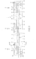
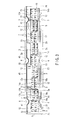
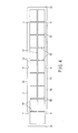
- the light-emitting device 1 serving as an illumination light source comprises a substrate 2, a plurality of light-emitting elements 3, and a pair of sealing members 4a and 4b.
- the substrate 2 is formed of a synthetic resin material such as a glass epoxy resin.
- the substrate 2 is formed into a long and thin shape having a pair of long sides 2a and 2b, and a pair of short sides 2c and 2d.
- the substrate 2 has a first surface 5a, second surface 5b positioned on the opposite side of the first surface 5a, and outer peripheral surface 5c connecting the first surface 5a and second surface 5b to each other. Both the first and second surfaces 5a and 5b are flat surfaces.
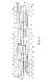
- the other power supply pattern 24b is inserted into the slit 12a of the pad 12 positioned at the right end of the substrate 2.
- the power supply terminals 25 of the power supply pattern 24b are inserted into the respective depressed parts 17 opened to the slit 12a.
- the power supply pattern 24b and pad 12 are electrically separated from each other by an insulating space positioned inside the slit 12a.
- the power supply terminals 25 of the power supply pattern 24b and the depressed parts 17 of the pad 12 are electrically separated from each other by providing insulating spaces between them.
- a power supply connector 26 is soldered to the positive electrode terminal 21 and negative electrode terminal 22.
- the power supply connector 26 is positioned on the first surface 5a of the substrate 2, and is electrically connected to a power supply circuit through lead wires 26a. Furthermore, the negative power supply conductor 14 and relay conductor 15 are short-circuited through a relay connector 27.
- the depressed part 45 intersects the bases of the branch lines 33 branching off from the common line 32. As a result, the branch lines 33 are left on the first surface 5a of the substrate 2 in a state where the branch lines 33 are electrically separated from each other.
Landscapes
- Engineering & Computer Science (AREA)
- Microelectronics & Electronic Packaging (AREA)
- Power Engineering (AREA)
- General Engineering & Computer Science (AREA)
- Computer Hardware Design (AREA)
- Physics & Mathematics (AREA)
- Manufacturing & Machinery (AREA)
- Condensed Matter Physics & Semiconductors (AREA)
- General Physics & Mathematics (AREA)
- Optics & Photonics (AREA)
- Led Device Packages (AREA)
- Fastening Of Light Sources Or Lamp Holders (AREA)
Applications Claiming Priority (2)
| Application Number | Priority Date | Filing Date | Title |
|---|---|---|---|
| JP2010029542A JP5515822B2 (ja) | 2010-02-12 | 2010-02-12 | 発光装置及び照明装置 |
| JP2011010021A JP2012151358A (ja) | 2011-01-20 | 2011-01-20 | 発光装置及び照明装置 |
Publications (2)
| Publication Number | Publication Date |
|---|---|
| EP2360417A2 true EP2360417A2 (de) | 2011-08-24 |
| EP2360417A3 EP2360417A3 (de) | 2013-09-18 |
Family
ID=44063774
Family Applications (1)
| Application Number | Title | Priority Date | Filing Date |
|---|---|---|---|
| EP11154159.5A Withdrawn EP2360417A3 (de) | 2010-02-12 | 2011-02-11 | Lichtemittierende Vorrichtung und Beleuchtungsvorrichtung |
Country Status (3)
| Country | Link |
|---|---|
| US (1) | US8616732B2 (de) |
| EP (1) | EP2360417A3 (de) |
| CN (1) | CN102194976B (de) |
Cited By (2)
| Publication number | Priority date | Publication date | Assignee | Title |
|---|---|---|---|---|
| EP2741328A1 (de) * | 2012-12-04 | 2014-06-11 | Toshiba Lighting & Technology Corporation | Lichtemittierende Vorrichtung und Leuchte |
| EP2765347A1 (de) * | 2013-02-07 | 2014-08-13 | Toshiba Lighting & Technology Corporation | Lichtemittierendes Modul, Lampe mit geradem Rohr und Leuchte |
Families Citing this family (9)
| Publication number | Priority date | Publication date | Assignee | Title |
|---|---|---|---|---|
| US20120268698A1 (en) * | 2011-04-21 | 2012-10-25 | E Ink Holdings Inc. | Color filter substrate and display device |
| TWI572054B (zh) | 2012-03-16 | 2017-02-21 | 晶元光電股份有限公司 | 高亮度發光二極體結構與其製造方法 |
| CN107658373B (zh) * | 2012-03-28 | 2020-01-21 | 晶元光电股份有限公司 | 发光二极管结构与其制造方法 |
| TWI533424B (zh) * | 2012-04-26 | 2016-05-11 | 旭德科技股份有限公司 | 封裝載板 |
| JP2014146661A (ja) * | 2013-01-28 | 2014-08-14 | Panasonic Corp | 発光モジュール、照明装置および照明器具 |
| KR101408871B1 (ko) * | 2013-02-21 | 2014-06-17 | 주식회사 씨엘포토닉스 | Led 조명모듈 |
| CN103334133B (zh) * | 2013-06-21 | 2015-09-02 | 深圳市通用科技有限公司 | 一种灯具反光杯的电镀制作工艺方法 |
| CN113658943A (zh) * | 2013-12-13 | 2021-11-16 | 晶元光电股份有限公司 | 发光装置及其制作方法 |
| CN114745842B (zh) * | 2020-12-24 | 2024-04-19 | 东友精细化工有限公司 | 电路板 |
Family Cites Families (28)
| Publication number | Priority date | Publication date | Assignee | Title |
|---|---|---|---|---|
| JPH1154769A (ja) | 1997-07-30 | 1999-02-26 | Toshiba Corp | 光実装部品およびその製造方法 |
| JP4045781B2 (ja) | 2001-08-28 | 2008-02-13 | 松下電工株式会社 | 発光装置 |
| KR20040092512A (ko) * | 2003-04-24 | 2004-11-04 | (주)그래픽테크노재팬 | 방열 기능을 갖는 반사판이 구비된 반도체 발광장치 |
| JP2005056653A (ja) | 2003-08-01 | 2005-03-03 | Fuji Photo Film Co Ltd | 光源装置 |
| KR100732267B1 (ko) | 2003-09-29 | 2007-06-25 | 마츠시타 덴끼 산교 가부시키가이샤 | 선형 광원장치 및 그 제조방법, 그리고 면 발광장치 |
| US20050285926A1 (en) | 2004-06-29 | 2005-12-29 | Fuji Photo Film Co., Ltd. | Light source assembly, method of producing light source assembly, and color thermal printer |
| EP1836071B1 (de) | 2004-12-30 | 2013-06-12 | GE Lighting Solutions, LLC | Lichtsignalanlage mit einer gleichförmigen lichtfläche |
| JP2006351708A (ja) | 2005-06-14 | 2006-12-28 | Toyoda Gosei Co Ltd | 発光ダイオードランプ及び光源装置 |
| KR100782798B1 (ko) | 2006-02-22 | 2007-12-05 | 삼성전기주식회사 | 기판 패키지 및 그 제조 방법 |
| KR101210090B1 (ko) | 2006-03-03 | 2012-12-07 | 엘지이노텍 주식회사 | 금속 코어 인쇄회로기판 및 이를 이용한 발광 다이오드패키징 방법 |
| JP2007311325A (ja) | 2006-04-17 | 2007-11-29 | Citizen Electronics Co Ltd | 導光板及びその製造方法とその導光板を用いたバックライトユニット |
| TW200802957A (en) | 2006-06-16 | 2008-01-01 | Gigno Technology Co Ltd | Light emitting diode module |
| JP5122098B2 (ja) | 2006-08-11 | 2013-01-16 | 株式会社トクヤマ | メタライズ基板、半導体装置 |
| JP4678391B2 (ja) | 2006-08-29 | 2011-04-27 | 東芝ライテック株式会社 | 照明装置 |
| US20080117619A1 (en) | 2006-11-21 | 2008-05-22 | Siew It Pang | Light source utilizing a flexible circuit carrier and flexible reflectors |
| JP2008166081A (ja) | 2006-12-27 | 2008-07-17 | Toshiba Lighting & Technology Corp | 照明装置及びこの照明装置を備えた照明器具 |
| JP4826470B2 (ja) | 2006-12-28 | 2011-11-30 | 日亜化学工業株式会社 | 発光装置 |
| JP2008166611A (ja) | 2006-12-28 | 2008-07-17 | Kyocera Corp | 発光素子アレイ、それを用いた光プリントヘッドおよび画像形成装置 |
| JP2008198782A (ja) | 2007-02-13 | 2008-08-28 | Toyoda Gosei Co Ltd | 発光装置 |
| JP4983347B2 (ja) | 2007-04-03 | 2012-07-25 | ソニー株式会社 | 発光装置及び光源装置 |
| US7938558B2 (en) | 2007-05-04 | 2011-05-10 | Ruud Lighting, Inc. | Safety accommodation arrangement in LED package/lens structure |
| JP2009054989A (ja) | 2007-07-31 | 2009-03-12 | Sharp Corp | 発光装置、照明装置及び当該照明装置を備えたクリーンルーム |
| JP2009040884A (ja) | 2007-08-09 | 2009-02-26 | Hitachi Ltd | 光反射部形成用樹脂組成物、その組成物の皮膜を有する配線基板とその製造方法、光半導体パッケージ、および照明装置 |
| US8042976B2 (en) | 2007-11-30 | 2011-10-25 | Taiyo Holdings Co., Ltd. | White hardening resin composition, hardened material, printed-wiring board and reflection board for light emitting device |
| WO2009090867A1 (ja) | 2008-01-15 | 2009-07-23 | Sekisui Chemical Co., Ltd. | レジスト材料及び積層体 |
| CN201302063Y (zh) | 2008-12-05 | 2009-09-02 | 上海芯光科技有限公司 | 无缝拼接式半导体平面光源模块 |
| US8348460B2 (en) | 2009-05-01 | 2013-01-08 | Abl Ip Holding Llc | Lighting apparatus with several light units arranged in a heatsink |
| TWI411143B (en) * | 2009-06-26 | 2013-10-01 | Led package structure with a plurality of standby pads for increasing wire-bonding yield and method for manufacturing the same |
-
2011
- 2011-02-10 US US13/024,376 patent/US8616732B2/en not_active Expired - Fee Related
- 2011-02-11 EP EP11154159.5A patent/EP2360417A3/de not_active Withdrawn
- 2011-02-11 CN CN201110037796.4A patent/CN102194976B/zh not_active Expired - Fee Related
Non-Patent Citations (1)
| Title |
|---|
| None |
Cited By (3)
| Publication number | Priority date | Publication date | Assignee | Title |
|---|---|---|---|---|
| EP2741328A1 (de) * | 2012-12-04 | 2014-06-11 | Toshiba Lighting & Technology Corporation | Lichtemittierende Vorrichtung und Leuchte |
| US9236551B2 (en) | 2012-12-04 | 2016-01-12 | Toshiba Lighting & Technology Corporation | Light emitting device and luminaire |
| EP2765347A1 (de) * | 2013-02-07 | 2014-08-13 | Toshiba Lighting & Technology Corporation | Lichtemittierendes Modul, Lampe mit geradem Rohr und Leuchte |
Also Published As
| Publication number | Publication date |
|---|---|
| US8616732B2 (en) | 2013-12-31 |
| US20110199772A1 (en) | 2011-08-18 |
| EP2360417A3 (de) | 2013-09-18 |
| CN102194976B (zh) | 2016-08-10 |
| CN102194976A (zh) | 2011-09-21 |
Similar Documents
| Publication | Publication Date | Title |
|---|---|---|
| US8616732B2 (en) | Light-emitting device and illumination device | |
| US8632212B2 (en) | Light-emitting device and illumination device | |
| JP5291268B1 (ja) | 発光モジュールおよびこれを用いた照明用光源、照明装置 | |
| US9196584B2 (en) | Light-emitting device and lighting apparatus using the same | |
| WO2011136236A1 (ja) | リードフレーム、配線板、発光ユニット、照明装置 | |
| CN101877382B (zh) | 发光器件封装和包括该发光器件封装的照明系统 | |
| US8816381B2 (en) | Light-emitting device, method of manufacturing light-emitting device, and illumination device | |
| TWI505519B (zh) | 發光二極體燈條及其製造方法 | |
| EP2397745A2 (de) | Lichtemittierende Vorrichtung und Leuchte | |
| EP3232482A1 (de) | Lichtemittierende vorrichtung | |
| WO2011024861A1 (ja) | 発光装置および照明装置 | |
| JP5562383B2 (ja) | ランプ及び照明装置 | |
| US20170077368A1 (en) | Light-emitting device | |
| JP5515822B2 (ja) | 発光装置及び照明装置 | |
| JP7154684B2 (ja) | 照明装置 | |
| JP6135199B2 (ja) | 発光装置 | |
| JP2014072149A (ja) | 照明用光源及び照明装置 | |
| JP6085459B2 (ja) | 照明装置 | |
| JP2012004412A (ja) | 発光装置及び照明装置 | |
| JP2012151358A (ja) | 発光装置及び照明装置 | |
| JP2011166036A (ja) | 発光装置及び照明装置 | |
| JP6704182B2 (ja) | 照明装置 | |
| RU160075U1 (ru) | Светодиодный излучатель | |
| JP2012156440A (ja) | 発光装置及び照明装置 | |
| TWI523271B (zh) | 插件式發光單元及發光裝置 |
Legal Events
| Date | Code | Title | Description |
|---|---|---|---|
| PUAI | Public reference made under article 153(3) epc to a published international application that has entered the european phase |
Free format text: ORIGINAL CODE: 0009012 |
|
| 17P | Request for examination filed |
Effective date: 20110211 |
|
| AK | Designated contracting states |
Kind code of ref document: A2 Designated state(s): AL AT BE BG CH CY CZ DE DK EE ES FI FR GB GR HR HU IE IS IT LI LT LU LV MC MK MT NL NO PL PT RO RS SE SI SK SM TR |
|
| AX | Request for extension of the european patent |
Extension state: BA ME |
|
| PUAL | Search report despatched |
Free format text: ORIGINAL CODE: 0009013 |
|
| AK | Designated contracting states |
Kind code of ref document: A3 Designated state(s): AL AT BE BG CH CY CZ DE DK EE ES FI FR GB GR HR HU IE IS IT LI LT LU LV MC MK MT NL NO PL PT RO RS SE SI SK SM TR |
|
| AX | Request for extension of the european patent |
Extension state: BA ME |
|
| RIC1 | Information provided on ipc code assigned before grant |
Ipc: F21V 19/00 20060101ALI20130814BHEP Ipc: F21V 31/00 20060101ALI20130814BHEP Ipc: H01L 33/54 20100101ALN20130814BHEP Ipc: H01L 25/075 20060101ALI20130814BHEP Ipc: F21K 99/00 20100101AFI20130814BHEP Ipc: F21Y 101/02 20060101ALN20130814BHEP Ipc: F21Y 103/00 20060101ALN20130814BHEP Ipc: H01L 33/60 20100101ALN20130814BHEP |
|
| 17Q | First examination report despatched |
Effective date: 20150127 |
|
| STAA | Information on the status of an ep patent application or granted ep patent |
Free format text: STATUS: THE APPLICATION IS DEEMED TO BE WITHDRAWN |
|
| 18D | Application deemed to be withdrawn |
Effective date: 20150609 |