EP2354846A2 - Optical irradiation equipment and optical irradiation method for nanoimprint lithography - Google Patents
Optical irradiation equipment and optical irradiation method for nanoimprint lithography Download PDFInfo
- Publication number
- EP2354846A2 EP2354846A2 EP11000620A EP11000620A EP2354846A2 EP 2354846 A2 EP2354846 A2 EP 2354846A2 EP 11000620 A EP11000620 A EP 11000620A EP 11000620 A EP11000620 A EP 11000620A EP 2354846 A2 EP2354846 A2 EP 2354846A2
- Authority
- EP
- European Patent Office
- Prior art keywords
- template
- transmission window
- radiation transmission
- optical irradiation
- cooling gas
- Prior art date
- Legal status (The legal status is an assumption and is not a legal conclusion. Google has not performed a legal analysis and makes no representation as to the accuracy of the status listed.)
- Withdrawn
Links
Images



Classifications
-
- H—ELECTRICITY
- H10—SEMICONDUCTOR DEVICES; ELECTRIC SOLID-STATE DEVICES NOT OTHERWISE PROVIDED FOR
- H10P—GENERIC PROCESSES OR APPARATUS FOR THE MANUFACTURE OR TREATMENT OF DEVICES COVERED BY CLASS H10
- H10P76/00—Manufacture or treatment of masks on semiconductor bodies, e.g. by lithography or photolithography
- H10P76/20—Manufacture or treatment of masks on semiconductor bodies, e.g. by lithography or photolithography of masks comprising organic materials
- H10P76/204—Manufacture or treatment of masks on semiconductor bodies, e.g. by lithography or photolithography of masks comprising organic materials of organic photoresist masks
- H10P76/2041—Photolithographic processes
- H10P76/2042—Photolithographic processes using lasers
-
- G—PHYSICS
- G03—PHOTOGRAPHY; CINEMATOGRAPHY; ANALOGOUS TECHNIQUES USING WAVES OTHER THAN OPTICAL WAVES; ELECTROGRAPHY; HOLOGRAPHY
- G03F—PHOTOMECHANICAL PRODUCTION OF TEXTURED OR PATTERNED SURFACES, e.g. FOR PRINTING, FOR PROCESSING OF SEMICONDUCTOR DEVICES; MATERIALS THEREFOR; ORIGINALS THEREFOR; APPARATUS SPECIALLY ADAPTED THEREFOR
- G03F7/00—Photomechanical, e.g. photolithographic, production of textured or patterned surfaces, e.g. printing surfaces; Materials therefor, e.g. comprising photoresists; Apparatus specially adapted therefor
- G03F7/0002—Lithographic processes using patterning methods other than those involving the exposure to radiation, e.g. by stamping
-
- B—PERFORMING OPERATIONS; TRANSPORTING
- B82—NANOTECHNOLOGY
- B82Y—SPECIFIC USES OR APPLICATIONS OF NANOSTRUCTURES; MEASUREMENT OR ANALYSIS OF NANOSTRUCTURES; MANUFACTURE OR TREATMENT OF NANOSTRUCTURES
- B82Y10/00—Nanotechnology for information processing, storage or transmission, e.g. quantum computing or single electron logic
-
- B—PERFORMING OPERATIONS; TRANSPORTING
- B82—NANOTECHNOLOGY
- B82Y—SPECIFIC USES OR APPLICATIONS OF NANOSTRUCTURES; MEASUREMENT OR ANALYSIS OF NANOSTRUCTURES; MANUFACTURE OR TREATMENT OF NANOSTRUCTURES
- B82Y40/00—Manufacture or treatment of nanostructures
-
- G—PHYSICS
- G03—PHOTOGRAPHY; CINEMATOGRAPHY; ANALOGOUS TECHNIQUES USING WAVES OTHER THAN OPTICAL WAVES; ELECTROGRAPHY; HOLOGRAPHY
- G03F—PHOTOMECHANICAL PRODUCTION OF TEXTURED OR PATTERNED SURFACES, e.g. FOR PRINTING, FOR PROCESSING OF SEMICONDUCTOR DEVICES; MATERIALS THEREFOR; ORIGINALS THEREFOR; APPARATUS SPECIALLY ADAPTED THEREFOR
- G03F7/00—Photomechanical, e.g. photolithographic, production of textured or patterned surfaces, e.g. printing surfaces; Materials therefor, e.g. comprising photoresists; Apparatus specially adapted therefor
- G03F7/20—Exposure; Apparatus therefor
- G03F7/2002—Exposure; Apparatus therefor with visible light or UV light, through an original having an opaque pattern on a transparent support, e.g. film printing, projection printing; by reflection of visible or UV light from an original such as a printed image
-
- G—PHYSICS
- G03—PHOTOGRAPHY; CINEMATOGRAPHY; ANALOGOUS TECHNIQUES USING WAVES OTHER THAN OPTICAL WAVES; ELECTROGRAPHY; HOLOGRAPHY
- G03F—PHOTOMECHANICAL PRODUCTION OF TEXTURED OR PATTERNED SURFACES, e.g. FOR PRINTING, FOR PROCESSING OF SEMICONDUCTOR DEVICES; MATERIALS THEREFOR; ORIGINALS THEREFOR; APPARATUS SPECIALLY ADAPTED THEREFOR
- G03F7/00—Photomechanical, e.g. photolithographic, production of textured or patterned surfaces, e.g. printing surfaces; Materials therefor, e.g. comprising photoresists; Apparatus specially adapted therefor
- G03F7/70—Microphotolithographic exposure; Apparatus therefor
- G03F7/708—Construction of apparatus, e.g. environment aspects, hygiene aspects or materials
- G03F7/70858—Environment aspects, e.g. pressure of beam-path gas, temperature
- G03F7/70866—Environment aspects, e.g. pressure of beam-path gas, temperature of mask or workpiece
- G03F7/70875—Temperature, e.g. temperature control of masks or workpieces via control of stage temperature
Definitions
- the present invention relates to an optical irradiation equipment and an optical irradiation method, and relates particularly to an optical irradiation equipment and an optical irradiation method which are ideal for the dry cleaning treatment of the surface of templates in a nanoimprint device.
- a pattern forming material layer is formed on a substrate such as a wafer, on which a pattern is to be formed, by applying a liquid photocurable resin, a template (a mold) on which a pattern being a negative of the pattern to be formed has been prepared is brought into contact with this pattern forming material layer, and in this condition the pattern forming material layer is irradiated with UV rays and cured. Then, a process to detach the template from the obtained layer of cured resin is performed (see JP-A-2000-194142 and US 2008/0090170 A1 (corresponding to JP-A- 2008-91782 )).
- an optical cleaning treatment device is used as the means for the cleaning treatment of glass substrates (see JP-A-8-236492 (1996 )).
- the following problems occur when the cleaning treatment of a template is performed.
- templates in the photo-nanoimprint technology templates from, for example, quartz glass are used, and the temperature control of the templates is extremely important from the aspects of the dimensional stability and the maintenance of the shape of the pattern.
- the template is irradiated with UV rays at the time of the optical cleaning treatment or is subjected to radiant heat from the UV radiation transmission window of the optical cleaning treatment device. Therefore, there is the problem that the temperature of the template increases.
- the present invention was made on the basis of the above-mentioned situation and has the object to provide an optical irradiation equipment and an optical irradiation method by means of which an irradiation with UV rays can be performed while an increase of the temperature of the object to be treated is suppressed.
- the optical irradiation equipment of the present invention which is provided with a cage body having an UV radiation transmission window, and an excimer lamp which is arranged in the interior of this cage body, is characterized in that gas flow openings being connected to a cooling gas supply mechanism or a cooling gas suction mechanism are present at the periphery of said UV radiation transmission window.
- the optical irradiation equipment of the present invention which is provided with a cage body having an UV radiation transmission window, and an excimer lamp which is arranged in the interior of this cage body, and which is arranged such that said UV radiation transmission window is positioned opposite and with a gap to the pattern surface of a template in a nanoimprint device, is characterized in that gas flow openings being connected to a cooling gas supply mechanism or a cooling gas suction mechanism are present at the periphery of said UV radiation transmission window, and cooling gas is passed via said gas flow openings into the gap between said UV radiation transmission window and said template.
- said excimer lamp has a discharge vessel with an overall shape of a flat plate, a high-voltage side electrode being arranged at one face of this discharge vessel, and an earth-side electrode being arranged at the other face of said discharge vessel, wherein the face of said discharge vessel at which said high-voltage side electrode is arranged is arranged such that it is positioned opposite to said UV radiation transmission window.
- the optical irradiation method of the present invention wherein an optical irradiation equipment being provided with a cage body having an UV radiation transmission window, and an excimer lamp which is arranged in the interior of this cage body, is arranged such that said UV radiation transmission window is positioned opposite and with a gap to the pattern surface of a template in a nanoimprint device, is characterized in that said template is irradiated with UV rays while a cooling gas is passed via gas flow openings which are provided at the periphery of said UV radiation transmission window and which are connected to a cooling gas supply mechanism or a cooling gas suction mechanism into the gap between said UV radiation transmission window and said template.
- the UV radiation transmission window is cooled by the cooling gas passed via the gas flow openings provided at the periphery of the UV radiation transmission window, an irradiation of the object to be treated with UV rays can be performed while an increase of the temperature of the object to be treated by means of radiant heat from said UV radiation transmission window is suppressed.
- a cooling of the template is performed in addition to the cooling of the UV radiation transmission window, an irradiation of the template with UV rays can be performed while an increase of the temperature of the template can be suppressed reliably.
- the excimer lamp is arranged such that the face of the discharge vessel at which the high-voltage side electrode is arranged is positioned such that it opposes the UV radiation transmission window
- no exterior discharge occurs between the excimer lamp and the cage body even though the distance between the other face of the discharge vessel at which the earth-side electrode is arranged and the inner face of the cage body is short, and therefore the thickness of the cage body can be rendered small and the distance between the one face of the discharge vessel emitting UV rays and the UV radiation transmission window can be rendered large, because of which an increase of the temperature of the UV radiation transmission window can be suppressed even more.
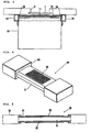
- FIG. 1 is a schematic explanatory view showing the configuration of an example for the optical irradiation equipment according to the present invention.
- FIG. 2 is a schematic explanatory sectional view of the optical irradiation equipment shown in FIG. 1 .
- FIG. 3 is a schematic explanatory sectional view showing a cross-section of a part of the optical irradiation equipment shown in FIG. 1 .
- FIG. 4 is a schematic oblique view of the excimer lamp in the optical irradiation equipment shown in FIG. 1 .
- FIG. 5 is a schematic explanatory sectional view of the excimer lamp shown in FIG. 4 .
- FIG. 6 is an explanatory view showing the schematic configuration of an example of a nanoimprint device being provided with the optical irradiation equipment of the present invention.
- FIG. 7 is a schematic explanatory view showing the condition in which the UV radiation transmission window of the optical irradiation equipment has been arranged via a gap opposite to the pattern surface of a template in the nanoimprint device shown in FIG. 6 .
- FIG. 8 is a schematic explanatory sectional view showing the condition in which cooling gas is passed into the gap between the template and the UV radiation transmission window by means of a cooling gas supply mechanism.
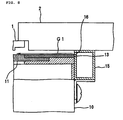
- FIG. 9 is a schematic explanatory sectional view showing a modification of the optical irradiation equipment according to the present invention.
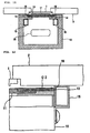
- FIG. 10 is a schematic explanatory sectional view showing another modification of the optical irradiation equipment according to the present invention.
- FIG. 11 is a schematic explanatory sectional view showing still another modification of the optical irradiation equipment according to the present invention.
- FIG. 12 is a schematic explanatory sectional view showing the condition in which cooling gas is passed into the gap between the template and the UV radiation transmission window by means of a cooling gas suction mechanism.
- FIG. 13 is a diagram of the temperature increase of the UV radiation transmission window and the template measured for embodiment 1 and comparison example 1.
- FIG. 1 is an explanatory view showing the configuration of an example for the optical irradiation equipment according to the present invention
- FIG. 2 is an explanatory sectional view of the optical irradiation equipment shown in FIG. 1 .
- This optical irradiation equipment 30 is employed for the optical cleaning treatment of the surfaces of templates in a nanoimprint device and is used by arranging a UV radiation transmission window 11 being discussed later such that it opposes the pattern surface of a template 1 held by means of a template holding mechanism 2 via a gap.
- a cage body 10 of this optical irradiation equipment 10 has an approximately block-shaped external shape.
- a lamp accommodation chamber S 1 and a circuit chamber S2 are arranged side by side via a partition wall 12, and in the upper face of the portion forming the lamp accommodation chamber S1 in the cage body 10 the UV radiation transmission window 11 consisting, for example, of quartz glass is provided such that it is fixed by a frame-shaped fixing plate 13.
- each gas passage element 15 has a plurality of gas flow openings 16 which are formed such that they are arranged side by side along one side face of said gas passage element 15. This one side face of each gas passage element 15 is fixed such that it is arranged in contact with the side face of the cage body 10 with the exception of an upper edge part 15a. By means of this the gas flow openings 16 are positioned at the periphery of the UV radiation transmission window 11 in the cage body 10.
- the gas passage elements 15 are connected to a cooling gas supply mechanism (not shown) via cooling gas flow pipes 17.
- the reference numeral 18 in FIG. 1 refers to a purge gas flow pipe supplying a purge gas such as, for example, nitrogen gas into the lamp accommodation chamber S 1.
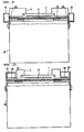
- FIG. 4 is an oblique view of the excimer lamp 20, and FIG. 5 is an explanatory sectional view of the excimer lamp 20 shown in FIG. 4 .
- This excimer lamp 20 has a discharge vessel 21 with an overall shape of a flat plate in the interior of which a discharge space S is formed. Sockets 24 are provided at both ends of this discharge vessel 21, and in the discharge space S of said discharge vessel 21 a gas for excimers is enclosed air-tightly.
- a reticulate high-voltage side electrode 22 is provided, while a reticulate earth-side electrode 23 is arranged at the other face of said discharge vessel 21.
- Both the high-voltage side electrode 22 and the earth-side electrode 23 are connected to a high-frequency power source (not shown). Further, the face of the excimer lamp 20 at which the high-voltage side electrode 22 of the discharge vessel 21 is arranged is positioned such that it opposes the UV radiation transmission window 11 in the cage body 10.
- a material with good permeability for vacuum UV radiation concretely silica glass such as synthetic quartz glass, sapphire glass and the like, can be used.
- the high-voltage side electrode 22 and the earth side electrode 23 For the material constituting the high-voltage side electrode 22 and the earth side electrode 23, a metallic material such as aluminium, nickel, gold and the like can be used. Further, the high-voltage side electrode 22 and the earth side electrode 23 can be formed by screen-printing a conductive paste containing the above-mentioned metallic material or by a vacuum deposition of the above-mentioned metallic material.
- a gas which generates excimers emitting vacuum UV radiation concretely a rare gas such as xenon, argon or krypton or a mixed gas consisting of a mixture from a rare gas and a halogen gas such as bromine, chlorine, iodine or fluorine, can be used.
- xenon gas results in 172 nm
- a mixed gas from argon and iodine results in 191 nm
- a mixed gas from argon and fluorine results in 193 nm.
- the enclosure pressure of the gas for excimers amounts to, for example, 10 to 100 kPa.
- FIG. 6 is an explanatory view showing the schematic configuration of an example of a nanoimprint device being provided with the optical irradiation equipment of the present invention.
- 1 refers to a template
- 2 refers to a template holding mechanism holding the template 1
- 3 refers to a chamber.
- 4 refers to a movable wafer stage, and on this wafer stage 4 a wafer chuck 4a holding a wafer W is arranged.
- 5 refers to an ink-jet application means to apply a liquid photocurable resin being the pattern forming material (imprint material) onto the surface of the wafer W.
- FIG. 6 refers to a pressure exerting mechanism
- 7 refers to a vibration-preventing table
- 8 refers to a stage surface plate
- 9 refers to a UV radiation light source radiating UV rays to the pattern forming material layer consisting of the photocurable resin which has been formed on the wafer W.
- 30 is an optical irradiation equipment being configured such as shown in FIG. 1 and FIG. 2 , and this optical irradiation equipment 30 is fixed on a transport arm 35 transporting said optical irradiation equipment 30 underneath the template 1.
- the wafer stage 4 on which a wafer W is held by the wafer chuck 4a is moved to a position beneath the application means 5.
- a pattern forming material layer consisting of the photocurable resin is formed on the wafer W.
- the wafer stage 4 is moved to a position beneath the template 1, and the template 1 is pressed into a contact with the pattern forming material layer having been formed on the wafer W by the pressure exerting mechanism 6.
- the pattern forming material layer is cured by means of radiating UV rays from the UV radiation light source 9 via the template 1 to the pattern forming material layer.
- the forming of the pattern at the wafer W is completed by subsequently peeling-off the template 1 from the obtained cured resin layer.
- the wafer stage 4 being loaded with a wafer W is retracted by moving it from the position beneath the template 1 to a lateral position, the optical irradiation equipment 30 is transported to the position beneath the template 1, and the UV radiation transmission window 11 (see FIG. 3 ) thereof is arranged such that it opposes the pattern surface of the template 1 via a gap.
- the distance between the outer face of the UV radiation transmission window 11 and the pattern surface of the template 1 amounts to 0.3 to 10.0 mm.
- the cooling gas supply mechanism is operated, and by doing so cooling gas is supplied via the cooling gas flow pipes 17 to the gas passage elements 15.
- cooling gas G1 ejected from the gas flow openings 16 formed in the gas passage elements 15 is passed into the gap between the UV radiation transmission window 11 and the template 1, as is shown in FIG. 8 .
- the excimer lamp 20 is lighted by means of which UV rays from the excimer lamp 20 are radiated to the pattern surface of the template 1 via the UV radiation transmission window 11 and an optical cleaning treatment of the template 1 is obtained.
- the optical irradiation equipment 30 is transported and retracted from the position beneath the template 1, the wafer stage 4 loaded with a wafer W is moved to the position beneath the template 1, and the forming of the pattern on this wafer W is performed.
- the flow amount of the cooling gas which is passed into the gap between the UV radiation transmission window 11 and the template 1 is, for example, 100 to 1000 1/min, and the temperature of the cooling gas is, for example, 10 to 35 °C.
- the time of the exposure of the template 1 to UV radiation is, for example, 3 to 3600 seconds.
- the UV radiation transmission window 11 and the template 1 are cooled by passing a cooling gas via gas flow openings 16 which are positioned at the periphery of the UV radiation transmission window 11 of the cage body 10 into the gap between the UV radiation transmission window 11 and the template 1 being the object to be treated, an UV irradiation treatment of said template 1 can be performed while an increase of the temperature of the template 1 because of the irradiation with UV rays and the radiant heat from the UV radiation transmission window 11 is suppressed reliably.
- the gas flow openings 16 are positioned at the periphery of the UV radiation transmission window 11.
- the specific locations of the gas passage elements 15 and the positions for the formation of the gas flow openings 16 can be suitably changed according to the dimensions of the template 1 being the object to be treated and the template holding mechanism 2 holding it.
- the optical irradiation equipment shown in FIG. 1 to FIG 3 is an example in which the width (the size in the left-right direction in FIG. 3 ) of the template holding mechanism 2 is larger than the width of the cage body 10, but if the width of the template holding mechanism 2 is the same as the width of the cage body 10, it is also possible as shown in FIG. 9 to use gas passage elements 15 in which a plurality of gas flow openings 16 has been formed side by side along the axial direction of the tube at central positions of one side, and to arrange these one sides of the gas passage elements 15 such that they are contacting the side faces of the cage body 10, with the exception of the regions above the central positions in which these gas flow openings 16 have been formed.
- the width of the template holding mechanism 2 is smaller than the width of the cage body 10, it is also possible as shown in FIG. 10 to use gas passage elements 15 in which a plurality of gas flow openings 16 has been formed side by side along the axial direction of the tube at the bottom face, and to arrange these gas passage elements 15 along both side edges of the upper face of the cage body 10 with a spacing in the upward direction from the upper face of said cage body 10.
- the width of the template holding mechanism 2 is larger than the width of the cage body 10, as shown in FIG. 11 also a configuration is possible in which the gas passage elements 15 are arranged at the upper inner faces in said cage body 10 and cooling gas is passed into the gap between the UV radiation transmission window 11 and the template 1 by ejecting the cooling gas from gas flow openings 16 formed at the periphery of the UV radiation transmission window 11 at the upper face of said cage body 10 via gas flow channels 14 extending from the interior of the gas passage elements 15 to the upper surface of the cage body 10.
- the gas passage elements 15 may also be connected to a cooling gas suction mechanism instead of a cooling gas supply mechanism.
- cooling gas G2 being present at the periphery of gas flow openings 16 which are formed in the gas passage elements 15 is drawn into these openings by the operation of the cooling gas suction mechanism, as is shown in FIG. 12 , and as a result the cooling gas is passed into the gap between the UV radiation transmission window 11 and the template 1.
- one gas passage element 15 is connected to a cooling gas supply mechanism while the other gas passage element 15 is connected to a cooling gas suction mechanism.
- the object to be treated by the optical irradiation equipment of the present invention is not limited to templates in nanoimprint devices. An application to various objects which require a treatment with UV irradiation is possible.
- the dimensions of the lamp accommodation chamber were 100 mm x 250 mm x 80 mm.
- the UV radiation transmission window was made from quartz glass and had a length and width of 60 x 60 mm and a thickness of 4 mm.
- the gas passage elements had an internal height and width of 8 mm x 17 mm and a length of 200 mm. Eight circular gas flow openings with a diameter of 2 mm were formed with a pitch of 20 mm.
- the material of the discharge vessel was quartz glass. In the interior of the discharge vessel xenon gas was enclosed. The light emitting length was 50 mm, the light emitting width was 45 mm, and the output was 15 W.
- This excimer lamp was arranged in the cage body 10 such that the face of the discharge vessel at which the high-voltage side electrode was arranged was positioned opposite to the UV radiation transmission window.
- the spacing between the excimer lamp and the UV radiation transmission window was 30 mm.
- a template consisting of quartz glass with dimensions of the pattern region of the pattern face of 53 mm x 53 mm and a thickness of 5 mm was prepared.
- the above-mentioned optical irradiation equipment was arranged at the pattern face of this template such that the UV radiation transmission window was positioned opposite to the pattern face of the template in a nanoimprint device via a gap of 1 mm, and K-thermocouples for a temperature measurement were mounted at the UV radiation transmission window and at the template. Further, an UV irradiation treatment of the template was performed by lighting the excimer lamp while air with a temperature of 25 °C being the cooling gas was passed via the gas flow openings into the gap between the UV radiation transmission window and the template by means of operating a gas supply mechanism connected to the gas passage elements. The flow amount of the cooling gas which was passed into the gap between the UV radiation transmission window and the template was 2001/min.
- the optical irradiation equipment prepared in embodiment 1 was used, an UV irradiation treatment of the template was performed in the same way except that no cooling gas was passed into the gap between the UV radiation transmission window and the template, and the relation between the time of the UV irradiation treatment of the template and the increase of the temperature of the template and the UV radiation transmission window was examined. The results are shown in FIG. 13 .
- A1 shows the curve of the temperature increase of the UV radiation transmission window in embodiment 1
- A2 shows the curve of the temperature increase of the template in embodiment 1
- B1 shows the curve of the temperature increase of the UV radiation transmission window in comparison example 1
- B2 shows the curve of the temperature increase of the template in comparison example 1.
Landscapes
- Engineering & Computer Science (AREA)
- Physics & Mathematics (AREA)
- Chemical & Material Sciences (AREA)
- Nanotechnology (AREA)
- General Physics & Mathematics (AREA)
- Health & Medical Sciences (AREA)
- Crystallography & Structural Chemistry (AREA)
- Environmental & Geological Engineering (AREA)
- Manufacturing & Machinery (AREA)
- Theoretical Computer Science (AREA)
- Condensed Matter Physics & Semiconductors (AREA)
- Life Sciences & Earth Sciences (AREA)
- Atmospheric Sciences (AREA)
- Mathematical Physics (AREA)
- Epidemiology (AREA)
- Toxicology (AREA)
- Public Health (AREA)
- Exposure Of Semiconductors, Excluding Electron Or Ion Beam Exposure (AREA)
- Shaping Of Tube Ends By Bending Or Straightening (AREA)
- Cleaning In General (AREA)
- Exposure And Positioning Against Photoresist Photosensitive Materials (AREA)
- Physical Or Chemical Processes And Apparatus (AREA)
Abstract
Description
- The present invention relates to an optical irradiation equipment and an optical irradiation method, and relates particularly to an optical irradiation equipment and an optical irradiation method which are ideal for the dry cleaning treatment of the surface of templates in a nanoimprint device.
- In the manufacture of semiconductor chips and biochips, recently the photo-nanoimprint technology has gained attention as a method by means of which it is possible to produce at lower costs as compared to the known pattern forming method using photolithography and etching.
- In the pattern forming method using this photo-nanoimprint technology, a pattern forming material layer is formed on a substrate such as a wafer, on which a pattern is to be formed, by applying a liquid photocurable resin, a template (a mold) on which a pattern being a negative of the pattern to be formed has been prepared is brought into contact with this pattern forming material layer, and in this condition the pattern forming material layer is irradiated with UV rays and cured. Then, a process to detach the template from the obtained layer of cured resin is performed (see
JP-A-2000-194142 US 2008/0090170 A1 (corresponding toJP-A- 2008-91782 - If in this pattern forming method contaminants and the like are present on the surface of the template, defects are generated in the obtained pattern. Therefore it is necessary to perform a cleaning treatment of the surface of the template. For the method to perform the cleaning treatment of the template, the wet cleaning method using an organic solvent or a chemical such as an alkali or an acid is known (see
US 2009/0267267 A1 (corresponding toJP-A-2009-266841 - In the manufacture of liquid crystal display elements, for example, an optical cleaning treatment device is used as the means for the cleaning treatment of glass substrates (see
JP-A-8-236492 (1996 - The present invention was made on the basis of the above-mentioned situation and has the object to provide an optical irradiation equipment and an optical irradiation method by means of which an irradiation with UV rays can be performed while an increase of the temperature of the object to be treated is suppressed.
- The object is solved with the optical irradiation equipment as claimed in
claim 1 and the optical irradiation method ofclaim 4. Preferred embodiments are described in the dependent claims. - The optical irradiation equipment of the present invention which is provided with a cage body having an UV radiation transmission window, and an excimer lamp which is arranged in the interior of this cage body, is characterized in that gas flow openings being connected to a cooling gas supply mechanism or a cooling gas suction mechanism are present at the periphery of said UV radiation transmission window.
- Then, the optical irradiation equipment of the present invention which is provided with a cage body having an UV radiation transmission window, and an excimer lamp which is arranged in the interior of this cage body, and which is arranged such that said UV radiation transmission window is positioned opposite and with a gap to the pattern surface of a template in a nanoimprint device, is characterized in that gas flow openings being connected to a cooling gas supply mechanism or a cooling gas suction mechanism are present at the periphery of said UV radiation transmission window, and cooling gas is passed via said gas flow openings into the gap between said UV radiation transmission window and said template.
- In the optical irradiation equipment of the present invention it is preferred that said excimer lamp has a discharge vessel with an overall shape of a flat plate, a high-voltage side electrode being arranged at one face of this discharge vessel, and an earth-side electrode being arranged at the other face of said discharge vessel, wherein the face of said discharge vessel at which said high-voltage side electrode is arranged is arranged such that it is positioned opposite to said UV radiation transmission window.
- The optical irradiation method of the present invention wherein an optical irradiation equipment being provided with a cage body having an UV radiation transmission window, and an excimer lamp which is arranged in the interior of this cage body, is arranged such that said UV radiation transmission window is positioned opposite and with a gap to the pattern surface of a template in a nanoimprint device, is characterized in that said template is irradiated with UV rays while a cooling gas is passed via gas flow openings which are provided at the periphery of said UV radiation transmission window and which are connected to a cooling gas supply mechanism or a cooling gas suction mechanism into the gap between said UV radiation transmission window and said template.
- As, according to the present invention, the UV radiation transmission window is cooled by the cooling gas passed via the gas flow openings provided at the periphery of the UV radiation transmission window, an irradiation of the object to be treated with UV rays can be performed while an increase of the temperature of the object to be treated by means of radiant heat from said UV radiation transmission window is suppressed.
- As, according to the configuration which passes cooling gas via the gas flow openings into the gap between the UV radiation transmission window and the template being the object to be treated, a cooling of the template is performed in addition to the cooling of the UV radiation transmission window, an irradiation of the template with UV rays can be performed while an increase of the temperature of the template can be suppressed reliably.
- As, according to the configuration in which the excimer lamp is arranged such that the face of the discharge vessel at which the high-voltage side electrode is arranged is positioned such that it opposes the UV radiation transmission window, no exterior discharge occurs between the excimer lamp and the cage body even though the distance between the other face of the discharge vessel at which the earth-side electrode is arranged and the inner face of the cage body is short, and therefore the thickness of the cage body can be rendered small and the distance between the one face of the discharge vessel emitting UV rays and the UV radiation transmission window can be rendered large, because of which an increase of the temperature of the UV radiation transmission window can be suppressed even more.
-
FIG. 1 is a schematic explanatory view showing the configuration of an example for the optical irradiation equipment according to the present invention. -
FIG. 2 is a schematic explanatory sectional view of the optical irradiation equipment shown inFIG. 1 . -
FIG. 3 is a schematic explanatory sectional view showing a cross-section of a part of the optical irradiation equipment shown inFIG. 1 . -
FIG. 4 is a schematic oblique view of the excimer lamp in the optical irradiation equipment shown inFIG. 1 . -
FIG. 5 is a schematic explanatory sectional view of the excimer lamp shown inFIG. 4 . -
FIG. 6 is an explanatory view showing the schematic configuration of an example of a nanoimprint device being provided with the optical irradiation equipment of the present invention. -
FIG. 7 is a schematic explanatory view showing the condition in which the UV radiation transmission window of the optical irradiation equipment has been arranged via a gap opposite to the pattern surface of a template in the nanoimprint device shown inFIG. 6 . -
FIG. 8 is a schematic explanatory sectional view showing the condition in which cooling gas is passed into the gap between the template and the UV radiation transmission window by means of a cooling gas supply mechanism. -
FIG. 9 is a schematic explanatory sectional view showing a modification of the optical irradiation equipment according to the present invention. -
FIG. 10 is a schematic explanatory sectional view showing another modification of the optical irradiation equipment according to the present invention. -
FIG. 11 is a schematic explanatory sectional view showing still another modification of the optical irradiation equipment according to the present invention. -
FIG. 12 is a schematic explanatory sectional view showing the condition in which cooling gas is passed into the gap between the template and the UV radiation transmission window by means of a cooling gas suction mechanism. -
FIG. 13 is a diagram of the temperature increase of the UV radiation transmission window and the template measured forembodiment 1 and comparison example 1. - In the following, embodiments of the present invention will be explained in detail.
FIG. 1 is an explanatory view showing the configuration of an example for the optical irradiation equipment according to the present invention, andFIG. 2 is an explanatory sectional view of the optical irradiation equipment shown inFIG. 1 . - This
optical irradiation equipment 30 is employed for the optical cleaning treatment of the surfaces of templates in a nanoimprint device and is used by arranging a UVradiation transmission window 11 being discussed later such that it opposes the pattern surface of atemplate 1 held by means of atemplate holding mechanism 2 via a gap. Acage body 10 of thisoptical irradiation equipment 10 has an approximately block-shaped external shape. In the interior of this cage body 10 a lampaccommodation chamber S 1 and a circuit chamber S2 are arranged side by side via apartition wall 12, and in the upper face of the portion forming the lamp accommodation chamber S1 in thecage body 10 the UVradiation transmission window 11 consisting, for example, of quartz glass is provided such that it is fixed by a frame-shaped fixing plate 13. - As is also shown in
FIG. 3 , a rectangular tube-shapedgas passage element 15 through which cooling gas is passed is provided along the upper edge part of both side faces of thecage body 10. To explain this concretely, eachgas passage element 15 has a plurality ofgas flow openings 16 which are formed such that they are arranged side by side along one side face of saidgas passage element 15. This one side face of eachgas passage element 15 is fixed such that it is arranged in contact with the side face of thecage body 10 with the exception of an upper edge part 15a. By means of this thegas flow openings 16 are positioned at the periphery of the UVradiation transmission window 11 in thecage body 10. Thegas passage elements 15 are connected to a cooling gas supply mechanism (not shown) via coolinggas flow pipes 17. - In the lamp accommodation chamber S1 in the
cage body 11 anexcimer lamp 20 is arranged, while in the circuit chamber S2 a step-up transformer 25 etc. is arranged. Thereference numeral 18 inFIG. 1 refers to a purge gas flow pipe supplying a purge gas such as, for example, nitrogen gas into the lampaccommodation chamber S 1. -
FIG. 4 is an oblique view of theexcimer lamp 20, andFIG. 5 is an explanatory sectional view of theexcimer lamp 20 shown inFIG. 4 . Thisexcimer lamp 20 has adischarge vessel 21 with an overall shape of a flat plate in the interior of which a discharge space S is formed.Sockets 24 are provided at both ends of thisdischarge vessel 21, and in the discharge space S of said discharge vessel 21 a gas for excimers is enclosed air-tightly. At one face of the discharge vessel 21 a reticulate high-voltage side electrode 22 is provided, while a reticulate earth-side electrode 23 is arranged at the other face of saiddischarge vessel 21. Both the high-voltage side electrode 22 and the earth-side electrode 23 are connected to a high-frequency power source (not shown). Further, the face of theexcimer lamp 20 at which the high-voltage side electrode 22 of thedischarge vessel 21 is arranged is positioned such that it opposes the UVradiation transmission window 11 in thecage body 10. - For the material constituting the
discharge vessel 21, a material with good permeability for vacuum UV radiation, concretely silica glass such as synthetic quartz glass, sapphire glass and the like, can be used. - For the material constituting the high-
voltage side electrode 22 and theearth side electrode 23, a metallic material such as aluminium, nickel, gold and the like can be used. Further, the high-voltage side electrode 22 and theearth side electrode 23 can be formed by screen-printing a conductive paste containing the above-mentioned metallic material or by a vacuum deposition of the above-mentioned metallic material. - For the gas for excimers enclosed in the discharge space S of the
discharge vessel 21, a gas which generates excimers emitting vacuum UV radiation, concretely a rare gas such as xenon, argon or krypton or a mixed gas consisting of a mixture from a rare gas and a halogen gas such as bromine, chlorine, iodine or fluorine, can be used. To show concrete examples for gases for excimers together with the wavelength of the emitted UV rays, xenon gas results in 172 nm, a mixed gas from argon and iodine results in 191 nm, and a mixed gas from argon and fluorine results in 193 nm. The enclosure pressure of the gas for excimers amounts to, for example, 10 to 100 kPa. -
FIG. 6 is an explanatory view showing the schematic configuration of an example of a nanoimprint device being provided with the optical irradiation equipment of the present invention. In this drawing, 1 refers to a template, 2 refers to a template holding mechanism holding thetemplate wafer stage 4 awafer chuck 4a holding a wafer W is arranged. 5 refers to an ink-jet application means to apply a liquid photocurable resin being the pattern forming material (imprint material) onto the surface of the wafer W. 6 refers to a pressure exerting mechanism, 7 refers to a vibration-preventing table, 8 refers to a stage surface plate, and 9 refers to a UV radiation light source radiating UV rays to the pattern forming material layer consisting of the photocurable resin which has been formed on the wafer W. 30 is an optical irradiation equipment being configured such as shown inFIG. 1 and FIG. 2 , and thisoptical irradiation equipment 30 is fixed on atransport arm 35 transporting saidoptical irradiation equipment 30 underneath thetemplate 1. - In such a nanoimprint device, the
wafer stage 4 on which a wafer W is held by thewafer chuck 4a is moved to a position beneath the application means 5. By means of applying a liquid photocurable resin onto the surface of the wafer W with this application means 5, a pattern forming material layer consisting of the photocurable resin is formed on the wafer W. Next, thewafer stage 4 is moved to a position beneath thetemplate 1, and thetemplate 1 is pressed into a contact with the pattern forming material layer having been formed on the wafer W by thepressure exerting mechanism 6. In this condition the pattern forming material layer is cured by means of radiating UV rays from the UVradiation light source 9 via thetemplate 1 to the pattern forming material layer. The forming of the pattern at the wafer W is completed by subsequently peeling-off thetemplate 1 from the obtained cured resin layer. - After such a forming of a pattern on a wafer W has been finished once or a plurality of times, the
wafer stage 4 being loaded with a wafer W is retracted by moving it from the position beneath thetemplate 1 to a lateral position, theoptical irradiation equipment 30 is transported to the position beneath thetemplate 1, and the UV radiation transmission window 11 (seeFIG. 3 ) thereof is arranged such that it opposes the pattern surface of thetemplate 1 via a gap. Here, the distance between the outer face of the UVradiation transmission window 11 and the pattern surface of thetemplate 1 amounts to 0.3 to 10.0 mm. - In the
optical irradiation equipment 30 the cooling gas supply mechanism is operated, and by doing so cooling gas is supplied via the coolinggas flow pipes 17 to thegas passage elements 15. Thus, cooling gas G1 ejected from thegas flow openings 16 formed in thegas passage elements 15 is passed into the gap between the UVradiation transmission window 11 and thetemplate 1, as is shown inFIG. 8 . Then, in this state, theexcimer lamp 20 is lighted by means of which UV rays from theexcimer lamp 20 are radiated to the pattern surface of thetemplate 1 via the UVradiation transmission window 11 and an optical cleaning treatment of thetemplate 1 is obtained. Afterwards, theoptical irradiation equipment 30 is transported and retracted from the position beneath thetemplate 1, thewafer stage 4 loaded with a wafer W is moved to the position beneath thetemplate 1, and the forming of the pattern on this wafer W is performed. - The flow amount of the cooling gas which is passed into the gap between the UV
radiation transmission window 11 and thetemplate 1 is, for example, 100 to 1000 1/min, and the temperature of the cooling gas is, for example, 10 to 35 °C. - The time of the exposure of the
template 1 to UV radiation is, for example, 3 to 3600 seconds. - As, according to the above-mentioned
optical irradiation equipment 30, the UVradiation transmission window 11 and thetemplate 1 are cooled by passing a cooling gas viagas flow openings 16 which are positioned at the periphery of the UVradiation transmission window 11 of thecage body 10 into the gap between the UVradiation transmission window 11 and thetemplate 1 being the object to be treated, an UV irradiation treatment of saidtemplate 1 can be performed while an increase of the temperature of thetemplate 1 because of the irradiation with UV rays and the radiant heat from the UVradiation transmission window 11 is suppressed reliably. - Because that face of the
excimer lamp 20, at which the high-voltage side electrode 22 of thedischarge vessel 21 is arranged is positioned such that it opposes the UVradiation transmission window 11, no exterior discharge occurs between theexcimer lamp 20 and thecage body 10 even though the distance between the other face of thedischarge vessel 21 at which the earth-side electrode 23 is arranged and the inner face of thecage body 10 is short, and therefore the thickness of thecage body 10 can be rendered small and the distance between the one face of thedischarge vessel 21 emitting UV rays and the UVradiation transmission window 11 can be rendered large, because of which an increase of the temperature of the UVradiation transmission window 11 can be suppressed even more. - In the foregoing, a mode to carry out the present invention has been explained, but the present invention is not limited to the above-mentioned mode. It is possible to add various modifications.
- In the present invention it suffices that the
gas flow openings 16 are positioned at the periphery of the UVradiation transmission window 11. The specific locations of thegas passage elements 15 and the positions for the formation of thegas flow openings 16 can be suitably changed according to the dimensions of thetemplate 1 being the object to be treated and thetemplate holding mechanism 2 holding it. - The optical irradiation equipment shown in
FIG. 1 to FIG 3 , for instance, is an example in which the width (the size in the left-right direction inFIG. 3 ) of thetemplate holding mechanism 2 is larger than the width of thecage body 10, but if the width of thetemplate holding mechanism 2 is the same as the width of thecage body 10, it is also possible as shown inFIG. 9 to usegas passage elements 15 in which a plurality ofgas flow openings 16 has been formed side by side along the axial direction of the tube at central positions of one side, and to arrange these one sides of thegas passage elements 15 such that they are contacting the side faces of thecage body 10, with the exception of the regions above the central positions in which thesegas flow openings 16 have been formed. - Further, if the width of the
template holding mechanism 2 is smaller than the width of thecage body 10, it is also possible as shown inFIG. 10 to usegas passage elements 15 in which a plurality ofgas flow openings 16 has been formed side by side along the axial direction of the tube at the bottom face, and to arrange thesegas passage elements 15 along both side edges of the upper face of thecage body 10 with a spacing in the upward direction from the upper face of saidcage body 10. - Further, if the width of the
template holding mechanism 2 is larger than the width of thecage body 10, as shown inFIG. 11 also a configuration is possible in which thegas passage elements 15 are arranged at the upper inner faces in saidcage body 10 and cooling gas is passed into the gap between the UVradiation transmission window 11 and thetemplate 1 by ejecting the cooling gas fromgas flow openings 16 formed at the periphery of the UVradiation transmission window 11 at the upper face of saidcage body 10 viagas flow channels 14 extending from the interior of thegas passage elements 15 to the upper surface of thecage body 10. - The
gas passage elements 15 may also be connected to a cooling gas suction mechanism instead of a cooling gas supply mechanism. With such a configuration, cooling gas G2 being present at the periphery ofgas flow openings 16 which are formed in thegas passage elements 15 is drawn into these openings by the operation of the cooling gas suction mechanism, as is shown inFIG. 12 , and as a result the cooling gas is passed into the gap between the UVradiation transmission window 11 and thetemplate 1.
Further, it is also possible that onegas passage element 15 is connected to a cooling gas supply mechanism while the othergas passage element 15 is connected to a cooling gas suction mechanism. - The object to be treated by the optical irradiation equipment of the present invention is not limited to templates in nanoimprint devices. An application to various objects which require a treatment with UV irradiation is possible.
- An optical irradiation equipment with the following specifications was prepared according to the configuration of
FIG. 1 to FIG. 3 . - The dimensions of the lamp accommodation chamber were 100 mm x 250 mm x 80 mm. The UV radiation transmission window was made from quartz glass and had a length and width of 60 x 60 mm and a thickness of 4 mm.
- The gas passage elements had an internal height and width of 8 mm x 17 mm and a length of 200 mm. Eight circular gas flow openings with a diameter of 2 mm were formed with a pitch of 20 mm.
- The material of the discharge vessel was quartz glass. In the interior of the discharge vessel xenon gas was enclosed. The light emitting length was 50 mm, the light emitting width was 45 mm, and the output was 15 W.
- This excimer lamp was arranged in the
cage body 10 such that the face of the discharge vessel at which the high-voltage side electrode was arranged was positioned opposite to the UV radiation transmission window. The spacing between the excimer lamp and the UV radiation transmission window was 30 mm. - For the object to be treated, a template consisting of quartz glass with dimensions of the pattern region of the pattern face of 53 mm x 53 mm and a thickness of 5 mm was prepared.
- The above-mentioned optical irradiation equipment was arranged at the pattern face of this template such that the UV radiation transmission window was positioned opposite to the pattern face of the template in a nanoimprint device via a gap of 1 mm, and K-thermocouples for a temperature measurement were mounted at the UV radiation transmission window and at the template. Further, an UV irradiation treatment of the template was performed by lighting the excimer lamp while air with a temperature of 25 °C being the cooling gas was passed via the gas flow openings into the gap between the UV radiation transmission window and the template by means of operating a gas supply mechanism connected to the gas passage elements. The flow amount of the cooling gas which was passed into the gap between the UV radiation transmission window and the template was 2001/min.
- The relation between the time of the UV irradiation treatment of the template and the increase of the temperature of the template and the UV radiation transmission window was examined. The results are shown in
FIG. 13 . - The optical irradiation equipment prepared in
embodiment 1 was used, an UV irradiation treatment of the template was performed in the same way except that no cooling gas was passed into the gap between the UV radiation transmission window and the template, and the relation between the time of the UV irradiation treatment of the template and the increase of the temperature of the template and the UV radiation transmission window was examined. The results are shown inFIG. 13 . - In
FIG. 13 , A1 shows the curve of the temperature increase of the UV radiation transmission window inembodiment 1, A2 shows the curve of the temperature increase of the template inembodiment 1, B1 shows the curve of the temperature increase of the UV radiation transmission window in comparison example 1, and B2 shows the curve of the temperature increase of the template in comparison example 1. - As is obvious from
FIG. 13 , it was confirmed that by means of the optical irradiation equipment according toembodiment 1 it was possible to perform an UV irradiation treatment while a temperature increase of the object to be treated was suppressed.
Claims (4)
- An optical irradiation equipment provided with a cage body having an UV radiation transmission window, and an excimer lamp which is arranged in an interior of said cage body, wherein gas flow openings being connected to one of a cooling gas supply mechanism and a cooling gas suction mechanism are provided at a periphery of said UV radiation transmission window.
- An optical irradiation equipment of claim 1, wherein the UV radiation transmission window is positioned opposite and with a gap to a pattern surface of a template in a nanoimprint device, and the cooling gas supply mechanism or cooling gas suction mechanism is provided for passing cooling gas via said gas flow openings into the gap between said UV radiation transmission window and said template.
- The optical irradiation equipment according to claim 1 or 2, wherein said excimer lamp has a discharge vessel with an overall shape of a flat plate, a high-voltage side electrode being arranged at one face of this discharge vessel, and an earth-side electrode being arranged at another face of said discharge vessel, wherein the face of said discharge vessel at which said high-voltage side electrode is arranged is positioned opposite to said UV radiation transmission window.
- An optical irradiation method wherein an optical irradiation equipment being provided with a cage body having an UV radiation transmission window positioned opposite and with a gap to a pattern surface of a template in a nanoimprint device, and an excimer lamp which is arranged in an interior of said cage body,
wherein said template is irradiated with UV rays while a cooling gas is passed via gas flow openings which are provided at a periphery of said UV radiation transmission window and which are connected to one of a cooling gas supply mechanism and a cooling gas suction mechanism into the gap between said UV radiation transmission window and said template.
Applications Claiming Priority (1)
| Application Number | Priority Date | Filing Date | Title |
|---|---|---|---|
| JP2010016127A JP5471514B2 (en) | 2010-01-28 | 2010-01-28 | Light processing equipment |
Publications (2)
| Publication Number | Publication Date |
|---|---|
| EP2354846A2 true EP2354846A2 (en) | 2011-08-10 |
| EP2354846A3 EP2354846A3 (en) | 2015-03-25 |
Family
ID=43881244
Family Applications (1)
| Application Number | Title | Priority Date | Filing Date |
|---|---|---|---|
| EP11000620.2A Withdrawn EP2354846A3 (en) | 2010-01-28 | 2011-01-26 | Optical irradiation equipment and optical irradiation method for nanoimprint lithography |
Country Status (6)
| Country | Link |
|---|---|
| US (1) | US8522802B2 (en) |
| EP (1) | EP2354846A3 (en) |
| JP (1) | JP5471514B2 (en) |
| KR (1) | KR101429322B1 (en) |
| CN (1) | CN102218414B (en) |
| TW (1) | TWI480681B (en) |
Families Citing this family (13)
| Publication number | Priority date | Publication date | Assignee | Title |
|---|---|---|---|---|
| JP5776631B2 (en) * | 2012-06-04 | 2015-09-09 | ウシオ電機株式会社 | Template cleaning method, pattern forming method, optical cleaning apparatus, and nanoimprint apparatus |
| JP5987522B2 (en) * | 2012-07-23 | 2016-09-07 | ウシオ電機株式会社 | Template cleaning light irradiation apparatus, nanoimprint apparatus, template cleaning method, and pattern forming method |
| JP6304965B2 (en) * | 2012-08-24 | 2018-04-04 | キヤノン株式会社 | Imprint apparatus, imprint method, and article manufacturing method using the same |
| JP6586827B2 (en) * | 2015-08-31 | 2019-10-09 | ウシオ電機株式会社 | UV treatment equipment |
| CN108475025B (en) | 2015-11-20 | 2021-02-26 | Asml荷兰有限公司 | Lithographic apparatus and method of operating a lithographic apparatus |
| JP6728911B2 (en) * | 2016-04-08 | 2020-07-22 | ウシオ電機株式会社 | UV treatment device |
| JP6733274B2 (en) * | 2016-04-11 | 2020-07-29 | ウシオ電機株式会社 | UV treatment device |
| KR102162392B1 (en) | 2016-07-08 | 2020-10-06 | 우시오덴키 가부시키가이샤 | Light cleaning treatment device |
| WO2018084133A1 (en) * | 2016-11-02 | 2018-05-11 | ウシオ電機株式会社 | Ultraviolet treatment device |
| US10903096B2 (en) * | 2018-04-06 | 2021-01-26 | Varian Semiconductor Equipment Associates, Inc. | System and apparatus for process chamber window cooling |
| US10921706B2 (en) | 2018-06-07 | 2021-02-16 | Canon Kabushiki Kaisha | Systems and methods for modifying mesa sidewalls |
| US10990004B2 (en) | 2018-07-18 | 2021-04-27 | Canon Kabushiki Kaisha | Photodissociation frame window, systems including a photodissociation frame window, and methods of using a photodissociation frame window |
| CN113488561B (en) * | 2021-07-14 | 2024-11-15 | 常州捷佳创智能装备有限公司 | Furnace equipment |
Citations (4)
| Publication number | Priority date | Publication date | Assignee | Title |
|---|---|---|---|---|
| JPH08236492A (en) | 1995-02-24 | 1996-09-13 | Ushio Inc | Light cleaning method |
| JP2000194142A (en) | 1998-12-25 | 2000-07-14 | Fujitsu Ltd | Pattern forming method and semiconductor device manufacturing method |
| US20080090170A1 (en) | 2006-10-04 | 2008-04-17 | Ikuo Yoneda | Pattern forming template and pattern forming method |
| US20090267267A1 (en) | 2008-04-21 | 2009-10-29 | Ikuo Yoneda | Imprint method |
Family Cites Families (25)
| Publication number | Priority date | Publication date | Assignee | Title |
|---|---|---|---|---|
| US4868450A (en) * | 1988-02-12 | 1989-09-19 | Colterjohn Jr Walter L | Radiation device |
| JP2888353B2 (en) * | 1989-10-13 | 1999-05-10 | 東京エレクトロン株式会社 | Exposure equipment |
| JPH04171453A (en) * | 1990-11-02 | 1992-06-18 | Fujitsu Ltd | Exposure method |
| JP2733155B2 (en) * | 1991-10-24 | 1998-03-30 | 松下電工株式会社 | Planar luminous body |
| US6254689B1 (en) * | 1999-03-09 | 2001-07-03 | Lucent Technologies Inc. | System and method for flash photolysis cleaning of a semiconductor processing chamber |
| JP2001035826A (en) * | 1999-05-14 | 2001-02-09 | Tokyo Cathode Laboratory Co Ltd | Wafer dry cleaning equipment |
| JP2002118087A (en) * | 2000-06-29 | 2002-04-19 | Dms Co Ltd | UV inspection equipment |
| JP4221561B2 (en) * | 2002-10-02 | 2009-02-12 | 株式会社ジーエス・ユアサコーポレーション | Excimer lamp |
| TW200501194A (en) * | 2003-05-19 | 2005-01-01 | Ushio Electric Inc | Excimer lamp lighting device |
| JP2005085591A (en) * | 2003-09-09 | 2005-03-31 | Lecip Corp | Discharge tube |
| DE10343323A1 (en) * | 2003-09-11 | 2005-04-07 | Carl Zeiss Smt Ag | Stamp lithography method and device and stamp for the stamp lithograph |
| JP4583813B2 (en) * | 2004-06-03 | 2010-11-17 | Nec液晶テクノロジー株式会社 | Lamp unit and flat fluorescent lamp |
| US7921859B2 (en) * | 2004-12-16 | 2011-04-12 | Sematech, Inc. | Method and apparatus for an in-situ ultraviolet cleaning tool |
| JP4595556B2 (en) * | 2005-01-20 | 2010-12-08 | ウシオ電機株式会社 | UV irradiation equipment |
| JP2006210239A (en) * | 2005-01-31 | 2006-08-10 | Ushio Inc | Flat type lamp |
| JP4784118B2 (en) * | 2005-03-18 | 2011-10-05 | ウシオ電機株式会社 | Flat type lamp |
| KR100797787B1 (en) * | 2005-06-03 | 2008-01-24 | 주식회사 아이엠티 | Dry cleaning system using laser |
| JP2005317555A (en) * | 2005-07-12 | 2005-11-10 | Quark Systems Co Ltd | Excimer lamp and excimer irradiation device |
| US7527695B2 (en) * | 2006-06-21 | 2009-05-05 | Asahi Glass Company, Limited | Apparatus and method for cleaning substrate |
| US8337959B2 (en) * | 2006-11-28 | 2012-12-25 | Nanonex Corporation | Method and apparatus to apply surface release coating for imprint mold |
| JP5004027B2 (en) * | 2008-04-22 | 2012-08-22 | 富士電機株式会社 | Imprint method and apparatus |
| JP2009268974A (en) * | 2008-05-08 | 2009-11-19 | Toppan Printing Co Ltd | Ultraviolet irradiation method and ultraviolet irradiation apparatus |
| JP2010016127A (en) * | 2008-07-02 | 2010-01-21 | Tohoku Univ | Ferroelectric material film, semiconductor devices having ferroelectric material film, and method of manufacturing these elements |
| JP4695679B2 (en) * | 2008-08-21 | 2011-06-08 | 株式会社東芝 | Template cleaning method and pattern forming method |
| US8394203B2 (en) * | 2008-10-02 | 2013-03-12 | Molecular Imprints, Inc. | In-situ cleaning of an imprint lithography tool |
-
2010
- 2010-01-28 JP JP2010016127A patent/JP5471514B2/en not_active Expired - Fee Related
- 2010-11-08 TW TW099138357A patent/TWI480681B/en not_active IP Right Cessation
- 2010-12-10 KR KR1020100126278A patent/KR101429322B1/en not_active Expired - Fee Related
-
2011
- 2011-01-24 CN CN201110029588.XA patent/CN102218414B/en not_active Expired - Fee Related
- 2011-01-26 US US13/013,875 patent/US8522802B2/en not_active Expired - Fee Related
- 2011-01-26 EP EP11000620.2A patent/EP2354846A3/en not_active Withdrawn
Patent Citations (6)
| Publication number | Priority date | Publication date | Assignee | Title |
|---|---|---|---|---|
| JPH08236492A (en) | 1995-02-24 | 1996-09-13 | Ushio Inc | Light cleaning method |
| JP2000194142A (en) | 1998-12-25 | 2000-07-14 | Fujitsu Ltd | Pattern forming method and semiconductor device manufacturing method |
| US20080090170A1 (en) | 2006-10-04 | 2008-04-17 | Ikuo Yoneda | Pattern forming template and pattern forming method |
| JP2008091782A (en) | 2006-10-04 | 2008-04-17 | Toshiba Corp | Pattern forming template, pattern forming method, and nanoimprint apparatus |
| US20090267267A1 (en) | 2008-04-21 | 2009-10-29 | Ikuo Yoneda | Imprint method |
| JP2009266841A (en) | 2008-04-21 | 2009-11-12 | Toshiba Corp | Nano-imprint method |
Also Published As
| Publication number | Publication date |
|---|---|
| CN102218414B (en) | 2015-03-11 |
| EP2354846A3 (en) | 2015-03-25 |
| US8522802B2 (en) | 2013-09-03 |
| TWI480681B (en) | 2015-04-11 |
| CN102218414A (en) | 2011-10-19 |
| KR101429322B1 (en) | 2014-08-11 |
| TW201202841A (en) | 2012-01-16 |
| US20110181188A1 (en) | 2011-07-28 |
| JP2011155160A (en) | 2011-08-11 |
| KR20110088364A (en) | 2011-08-03 |
| JP5471514B2 (en) | 2014-04-16 |
Similar Documents
| Publication | Publication Date | Title |
|---|---|---|
| US8522802B2 (en) | Optical irradiation equipment and optical irradiation method | |
| JP5421378B2 (en) | In-situ cleaning of imprint lithography tools | |
| JP5861696B2 (en) | Light irradiation device | |
| JP2015122373A (en) | Imprint apparatus, foreign matter removing method, and article manufacturing method | |
| TWI583525B (en) | A template cleaning method, a pattern forming method, a light cleaning apparatus, and a nanoimprint apparatus | |
| US20080296258A1 (en) | Plenum reactor system | |
| US20120223631A1 (en) | Emitting apparatus for washing light nanoimprint template and method for the same | |
| WO2018173344A1 (en) | Exposure device, substrate treatment device, substrate exposure method, and substrate treatment method | |
| JP2012204381A (en) | Resin removal method and resin removal device | |
| JP2014007260A (en) | Imprint device, housing case, and method for manufacturing article | |
| US20210185793A1 (en) | Adhesive material removal from photomask in ultraviolet lithography application | |
| KR20240037848A (en) | Cleaning apparatus, cleaning method, imprint apparatus, and method for manufacturing an article | |
| JP2012176341A (en) | Light processing device | |
| JP2012176339A (en) | Light treatment apparatus | |
| JP2011245384A (en) | Light irradiation device | |
| US20130160793A1 (en) | Plasma generating apparatus and process for simultaneous exposure of a workpiece to electromagnetic radiation and plasma | |
| JP2025099769A (en) | Cleaning equipment, imprinting equipment, cleaning method and method for manufacturing article | |
| KR100621788B1 (en) | Ozone asher device | |
| TWI410288B (en) | In-situ cleaning of an imprint lithography tool | |
| JP6374735B2 (en) | Vacuum processing apparatus and dry cleaning method | |
| US20070148560A1 (en) | Thin film pattern forming device and method | |
| JP2012176340A (en) | Light treatment apparatus |
Legal Events
| Date | Code | Title | Description |
|---|---|---|---|
| PUAI | Public reference made under article 153(3) epc to a published international application that has entered the european phase |
Free format text: ORIGINAL CODE: 0009012 |
|
| AK | Designated contracting states |
Kind code of ref document: A2 Designated state(s): AL AT BE BG CH CY CZ DE DK EE ES FI FR GB GR HR HU IE IS IT LI LT LU LV MC MK MT NL NO PL PT RO RS SE SI SK SM TR |
|
| AX | Request for extension of the european patent |
Extension state: BA ME |
|
| PUAL | Search report despatched |
Free format text: ORIGINAL CODE: 0009013 |
|
| AK | Designated contracting states |
Kind code of ref document: A3 Designated state(s): AL AT BE BG CH CY CZ DE DK EE ES FI FR GB GR HR HU IE IS IT LI LT LU LV MC MK MT NL NO PL PT RO RS SE SI SK SM TR |
|
| AX | Request for extension of the european patent |
Extension state: BA ME |
|
| RIC1 | Information provided on ipc code assigned before grant |
Ipc: G03F 7/00 20060101AFI20150218BHEP Ipc: G03F 7/20 20060101ALI20150218BHEP |
|
| 17P | Request for examination filed |
Effective date: 20150521 |
|
| RBV | Designated contracting states (corrected) |
Designated state(s): AL AT BE BG CH CY CZ DE DK EE ES FI FR GB GR HR HU IE IS IT LI LT LU LV MC MK MT NL NO PL PT RO RS SE SI SK SM TR |
|
| RAP1 | Party data changed (applicant data changed or rights of an application transferred) |
Owner name: USHIO DENKI KABUSHIKI KAISHA |
|
| RAP1 | Party data changed (applicant data changed or rights of an application transferred) |
Owner name: USHIO DENKI KABUSHIKI KAISHA |
|
| GRAP | Despatch of communication of intention to grant a patent |
Free format text: ORIGINAL CODE: EPIDOSNIGR1 |
|
| RIC1 | Information provided on ipc code assigned before grant |
Ipc: B82Y 10/00 20110101ALI20190703BHEP Ipc: G03F 7/00 20060101AFI20190703BHEP Ipc: G03F 7/20 20060101ALI20190703BHEP Ipc: B82Y 40/00 20110101ALI20190703BHEP |
|
| INTG | Intention to grant announced |
Effective date: 20190802 |
|
| RIN1 | Information on inventor provided before grant (corrected) |
Inventor name: FUJITSUGU, HIDEKI Inventor name: NAKASHIMA, AKINOBU Inventor name: SUGIOKA, SHINJI Inventor name: YAMAGUCHI, MASANORI |
|
| STAA | Information on the status of an ep patent application or granted ep patent |
Free format text: STATUS: THE APPLICATION IS DEEMED TO BE WITHDRAWN |
|
| 18D | Application deemed to be withdrawn |
Effective date: 20191213 |