EP2348524B1 - Method for recovering pattern on silicon substrate - Google Patents
Method for recovering pattern on silicon substrate Download PDFInfo
- Publication number
- EP2348524B1 EP2348524B1 EP11151363.6A EP11151363A EP2348524B1 EP 2348524 B1 EP2348524 B1 EP 2348524B1 EP 11151363 A EP11151363 A EP 11151363A EP 2348524 B1 EP2348524 B1 EP 2348524B1
- Authority
- EP
- European Patent Office
- Prior art keywords
- patterns
- silicon substrate
- foreign substances
- gas
- heating
- Prior art date
- Legal status (The legal status is an assumption and is not a legal conclusion. Google has not performed a legal analysis and makes no representation as to the accuracy of the status listed.)
- Active
Links
Images


Classifications
-
- H—ELECTRICITY
- H10—SEMICONDUCTOR DEVICES; ELECTRIC SOLID-STATE DEVICES NOT OTHERWISE PROVIDED FOR
- H10P—GENERIC PROCESSES OR APPARATUS FOR THE MANUFACTURE OR TREATMENT OF DEVICES COVERED BY CLASS H10
- H10P70/00—Cleaning of wafers, substrates or parts of devices
- H10P70/10—Cleaning before device manufacture, i.e. Begin-Of-Line process
- H10P70/12—Cleaning before device manufacture, i.e. Begin-Of-Line process by dry cleaning only
- H10P70/125—Cleaning before device manufacture, i.e. Begin-Of-Line process by dry cleaning only with gaseous HF
-
- H—ELECTRICITY
- H10—SEMICONDUCTOR DEVICES; ELECTRIC SOLID-STATE DEVICES NOT OTHERWISE PROVIDED FOR
- H10P—GENERIC PROCESSES OR APPARATUS FOR THE MANUFACTURE OR TREATMENT OF DEVICES COVERED BY CLASS H10
- H10P70/00—Cleaning of wafers, substrates or parts of devices
- H10P70/20—Cleaning during device manufacture
-
- H—ELECTRICITY
- H10—SEMICONDUCTOR DEVICES; ELECTRIC SOLID-STATE DEVICES NOT OTHERWISE PROVIDED FOR
- H10P—GENERIC PROCESSES OR APPARATUS FOR THE MANUFACTURE OR TREATMENT OF DEVICES COVERED BY CLASS H10
- H10P70/00—Cleaning of wafers, substrates or parts of devices
-
- H—ELECTRICITY
- H10—SEMICONDUCTOR DEVICES; ELECTRIC SOLID-STATE DEVICES NOT OTHERWISE PROVIDED FOR
- H10P—GENERIC PROCESSES OR APPARATUS FOR THE MANUFACTURE OR TREATMENT OF DEVICES COVERED BY CLASS H10
- H10P72/00—Handling or holding of wafers, substrates or devices during manufacture or treatment thereof
- H10P72/04—Apparatus for manufacture or treatment
- H10P72/0402—Apparatus for fluid treatment
- H10P72/0406—Apparatus for fluid treatment for cleaning followed by drying, rinsing, stripping, blasting or the like
-
- H—ELECTRICITY
- H10—SEMICONDUCTOR DEVICES; ELECTRIC SOLID-STATE DEVICES NOT OTHERWISE PROVIDED FOR
- H10P—GENERIC PROCESSES OR APPARATUS FOR THE MANUFACTURE OR TREATMENT OF DEVICES COVERED BY CLASS H10
- H10P95/00—Generic processes or apparatus for manufacture or treatments not covered by the other groups of this subclass
- H10P95/90—Thermal treatments, e.g. annealing or sintering
Definitions
- the present invention relates to a pattern forming method.
- fine circuit patterns are formed on a silicon substrate (semiconductor wafer) by a photolithography process.
- predetermined patterns e.g., lines, holes or the like, are formed on a silicon substrate by a process for coating, exposing and developing a photoresist, an etching process using the photoresist as a mask, and the like.
- a polymer (so-called sidewall polymer) may be adhered to sidewalls of the patterns.
- a technique for removing the sidewall polymer there has been known a wet cleaning technique using a cleaning fluid including hydrogen fluoride, methanol and the like (see, e.g., Japanese Patent Application Publication No. H11-340183 ).
- a line width of the patterns formed by the photolithography process tends to be reduced from, e.g., about 56 nm to about 43 nm and further to about 32 nm.
- the formation of the ultra-fine patterns causes the following problems.
- the spaces between the patterns may be filled with the foreign substance, or the foreign substances may cause collapse of the patterns. Further, in this case, it is not proper to perform the wet etching process. Conventionally, the silicon substrate in which such phenomenon occurs has been destroyed. Therefore, it is required to develop a method and an apparatus capable of recovering a shape of patterns on a silicon substrate by removing foreign substance grown between the patterns.
- Embodiments of the present invention can provide a method capable of recovering a shape of patterns, formed on a silicon substrate by etching, by removing foreign substance frown between the patterns.
- Fig. 1 schematically shows an example of patterns to be recovered by a method in accordance with the embodiment of the present invention.
- patterns 110 which are formed of lines spaced apart from each other at regular intervals, are formed on a silicon substrate (semiconductor wafer) W by etching. Further, spaces 111 are formed between the patterns 110. In the invention, the widths of the patterns 110 and the spaces 111 are not greater than about 32 nm.
- Each of the patterns 110 on a silicon substrate W includes, e.g., a single crystal silicon layer 100, an SiO 2 layer 101, a polysilicon layer 102, an SiO 2 layer 103, an SiN layer 104, an SiO 2 layer 105 and the like which are laminated in that order from the bottom.
- a method for recovering patterns on a silicon substrate in accordance with the embodiment of the present invention will be described with reference to Figs. 2A to 2C .
- Fig. 2A upon completion of an etching process, the spaces 111 are formed between the patterns 110, and the patterns 110 are separated from each other.
- the etched silicon substrate W is left in the air, foreign substances 112 are grown between the patterns 110, as shown in Fig. 2B . Further, as shown in the left side of Fig. 2B , the spaces 111 between the patterns 110 are filled with the foreign substances 112 so that the patterns 110 adjacent to each other are connected through the foreign substances 112. Moreover, as shown in the right side of Fig. 2B , the foreign substances 112 may cause the collapse of the patterns 110. Such phenomenon do not occur when the patterns 110 and the spaces 111 have a larger width (e.g., about 56 nm).
- the foreign substances 112 are generated by reaction between ammonia in the air and fluorine remaining in the patterns 110 during the etching.
- a gas containing fluorine is often used as an etching gas, and the foreign substances 112 contain at least ammonium silicofluoride.
- such phenomenon occurs when the silicon substrate W is left in the air for, e.g., about a month. Time duration in which such phenomenon occurs can be shortened to about 24 hours if an accelerated test is performed on the substrate W in the state shown in Fig. 2A under the condition of high humidity (of about 85%) and high temperature (of about 85°C).
- the patterns 110 are recovered from the state shown in Fig. 2B to the state shown in Fig. 2C by removing the foreign substances 112 grown between the patterns 110.
- the shape of the patterns 110 is recovered by removing the foreign substances 112 by heating the silicon substrate W accommodated in a chamber to a temperature of about 160°C or higher and preferably to a temperature between about 200°C to 500°C.
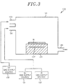
- Fig. 3 shows a configuration of a pattern recovery apparatus 120 for use in recovering patterns on a silicon substrate in accordance with the present embodiment.
- the pattern recovery apparatus 120 for use in recovering patterns on the silicon substrate includes a chamber 121 having an inner space that can be airtightly sealed.
- a mounting table 122 for mounting thereon the silicon substrate W. Further, a heater 127 serving as a heating unit is provided in the mounting table 122.
- an HF (hydrogen fluoride) gas inlet 123 for introducing HF gas into the chamber 121
- a heat treatment atmosphere gas inlet 124 for introducing a heat treatment atmosphere gas (N 2 , Ar or the like)
- a gas exhaust unit 125 for exhausting gas from the chamber 121.
- the HF gas inlet 123 is connected to an HF gas supply source 130
- the heat treatment atmosphere gas inlet 124 is connected to an N 2 gas supply source 131 and an Ar gas supply source 132.
- a vacuum pump (not shown) is connected to the gas exhaust unit 125.
- the silicon substrate W is loaded into the chamber 121 of the pattern recovery apparatus 120 having the above-described configuration, and then is mounted on the mounting table 122.
- the silicon substrate W is heated to a temperature of about 160°C or higher.
- the inner space of the chamber 121 is preferably set to, e.g., the atmosphere of N 2 gas, Ar gas or the gaseous mixture thereof introduced from the heat treatment atmosphere gas inlet 124.
- the inner space of the chamber 121 may be set to the atmospheric atmosphere during the heating.
- the melting point of ammonium silicofluoride at an atmospheric pressure is about 160°C.
- the heating temperature is preferably set to about 160°C or higher, and more preferably set between 200°C and 500°C. By increasing the heating temperature to about 200°C or higher, the foreign substances 112 can be effectively removed.
- the maximum heating temperature is set to about 500°C because the heating temperature higher than 500°C causes adverse effects on the silicon substrate W forming a semiconductor device.
- the patterns recovery process was performed by heating the silicon substrate W in the state shown in Fig. 2B to about 200°C in the N 2 gas atmosphere under an atmospheric pressure for about 180 seconds.
- the foreign substances 112 grown between the patterns 110 were removed, and the shape of the collapsed patterns 110 shown in the right side of Fig. 2B was recovered to the original state (line shape) shown in Fig. 2C .
- the same result was obtained even when the heating temperature was set to about 300°C.
- the heating process for recovering the patterns was performed in the atmospheric atmosphere, the patterns were insufficiently recovered at the heating temperature of about 200°C. However, the same result as that obtained in the N 2 gas atmosphere was obtained by increasing the heating temperature to about 300°C. Alternatively, the heating process may be performed in the depressurized atmosphere.
- the above-described heating process by which the foreign substances 112 grown between the patterns 110 is removed, may be insufficient to recover the shape of the patterns 110. In that case, it is considered that the foreign substances 112 contain silicon dioxide by reaction between the ammonium silicofluoride and moisture in the air.
- the patterns were recovered by performing the exposing process for exposing the silicon substrate in the state shown in Fig. 2B to the HF gas atmosphere and the heating process sequentially under the following conditions.
- the heating process is performed after the exposing process for exposing the silicon substrate to the HF gas atmosphere in the above test example 2, the exposing process may be performed after the heating process. Alternatively, the exposing process and the heating process may be performed simultaneously.
- defects may occur on a silicon-based material on the substrate by reaction of residual fluorine (see, e.g., Japanese Patent Application Publication No. H8-264507 ).
- a removing process for removing residual fluorine by irradiating a hydrogencontaining plasma from a plasma generator installed in the chamber 121.
Landscapes
- Cleaning Or Drying Semiconductors (AREA)
- Drying Of Semiconductors (AREA)
- Internal Circuitry In Semiconductor Integrated Circuit Devices (AREA)
- Crystals, And After-Treatments Of Crystals (AREA)
- Silicon Compounds (AREA)
Applications Claiming Priority (1)
| Application Number | Priority Date | Filing Date | Title |
|---|---|---|---|
| JP2010009979A JP5629098B2 (ja) | 2010-01-20 | 2010-01-20 | シリコン基板上のパターン修復方法 |
Publications (3)
| Publication Number | Publication Date |
|---|---|
| EP2348524A2 EP2348524A2 (en) | 2011-07-27 |
| EP2348524A3 EP2348524A3 (en) | 2011-11-09 |
| EP2348524B1 true EP2348524B1 (en) | 2019-03-20 |
Family
ID=44022937
Family Applications (1)
| Application Number | Title | Priority Date | Filing Date |
|---|---|---|---|
| EP11151363.6A Active EP2348524B1 (en) | 2010-01-20 | 2011-01-19 | Method for recovering pattern on silicon substrate |
Country Status (6)
| Country | Link |
|---|---|
| US (1) | US20110174337A1 (enExample) |
| EP (1) | EP2348524B1 (enExample) |
| JP (1) | JP5629098B2 (enExample) |
| KR (1) | KR20110085929A (enExample) |
| CN (1) | CN102140638A (enExample) |
| TW (1) | TWI534857B (enExample) |
Families Citing this family (7)
| Publication number | Priority date | Publication date | Assignee | Title |
|---|---|---|---|---|
| US8440573B2 (en) * | 2010-01-26 | 2013-05-14 | Lam Research Corporation | Method and apparatus for pattern collapse free wet processing of semiconductor devices |
| CN105990096B (zh) * | 2015-02-15 | 2020-03-27 | 盛美半导体设备(上海)股份有限公司 | 半导体结构的清洗方法 |
| JP6533576B2 (ja) * | 2015-07-13 | 2019-06-19 | 富士フイルム株式会社 | パターン構造の処理方法、電子デバイスの製造方法およびパターン構造の倒壊抑制用処理液 |
| JP6466315B2 (ja) * | 2015-12-25 | 2019-02-06 | 東京エレクトロン株式会社 | 基板処理方法及び基板処理システム |
| JP6875811B2 (ja) | 2016-09-16 | 2021-05-26 | 株式会社Screenホールディングス | パターン倒壊回復方法、基板処理方法および基板処理装置 |
| JP2021022598A (ja) * | 2019-07-24 | 2021-02-18 | 東京エレクトロン株式会社 | 基板処理方法、基板処理装置及び配線パターン形成システム |
| JP7130791B2 (ja) * | 2021-02-08 | 2022-09-05 | 株式会社Screenホールディングス | 基板処理方法および基板処理装置 |
Citations (1)
| Publication number | Priority date | Publication date | Assignee | Title |
|---|---|---|---|---|
| US20090191340A1 (en) * | 2007-12-27 | 2009-07-30 | Shigeki Tozawa | Substrate processing method and system |
Family Cites Families (23)
| Publication number | Priority date | Publication date | Assignee | Title |
|---|---|---|---|---|
| JPH0319217A (ja) * | 1989-06-15 | 1991-01-28 | Nec Corp | 微細パターン形成方法 |
| US5017998A (en) * | 1989-09-14 | 1991-05-21 | Fujitsu Limited | Semiconductor device using SOI substrate |
| JP2632262B2 (ja) | 1991-08-20 | 1997-07-23 | 大日本スクリーン製造株式会社 | シリコンウエハ上のコンタクトホール内の自然酸化膜の除去方法 |
| JPH05129263A (ja) * | 1991-11-01 | 1993-05-25 | Kawasaki Steel Corp | 半導体基板の処理方法 |
| JPH05326478A (ja) * | 1992-05-26 | 1993-12-10 | Nippon Steel Corp | ウェーハの洗浄方法およびその装置 |
| JPH08264507A (ja) | 1995-03-20 | 1996-10-11 | Matsushita Electron Corp | シリコンのエッチング方法 |
| JPH11340183A (ja) | 1998-05-27 | 1999-12-10 | Morita Kagaku Kogyo Kk | 半導体装置用洗浄液およびそれを用いた半導体装置の製 造方法 |
| KR100486690B1 (ko) * | 2002-11-29 | 2005-05-03 | 삼성전자주식회사 | 기판 이송 모듈의 오염을 제어할 수 있는 기판 처리 장치및 방법 |
| US7877161B2 (en) * | 2003-03-17 | 2011-01-25 | Tokyo Electron Limited | Method and system for performing a chemical oxide removal process |
| US7094613B2 (en) * | 2003-10-21 | 2006-08-22 | Applied Materials, Inc. | Method for controlling accuracy and repeatability of an etch process |
| KR100542464B1 (ko) * | 2003-11-20 | 2006-01-11 | 학교법인 한양학원 | 원자력간 현미경 리소그래피 기술을 이용한 극자외선 노광공정용 반사형 다층 박막 미러의 제조방법 |
| JP5073482B2 (ja) * | 2005-03-31 | 2012-11-14 | 東京エレクトロン株式会社 | シリコン酸化膜の製造方法、その制御プログラム、記憶媒体及びプラズマ処理装置 |
| JP5319868B2 (ja) * | 2005-10-17 | 2013-10-16 | ルネサスエレクトロニクス株式会社 | 半導体装置の製造方法 |
| US20070224811A1 (en) * | 2006-03-16 | 2007-09-27 | Xinming Wang | Substrate processing method and substrate processing apparatus |
| JP2007311540A (ja) * | 2006-05-18 | 2007-11-29 | Renesas Technology Corp | 半導体装置の製造方法 |
| JP5233097B2 (ja) * | 2006-08-15 | 2013-07-10 | 東京エレクトロン株式会社 | 基板処理方法、基板処理装置及び記憶媒体 |
| US20080045030A1 (en) * | 2006-08-15 | 2008-02-21 | Shigeru Tahara | Substrate processing method, substrate processing system and storage medium |
| JP4961894B2 (ja) * | 2006-08-25 | 2012-06-27 | 東京エレクトロン株式会社 | 基板処理装置、基板処理方法及び記憶媒体 |
| US20080085090A1 (en) * | 2006-10-10 | 2008-04-10 | Meek David W | Crimp and crimp mechanism for fiber optic connector |
| JP5204964B2 (ja) * | 2006-10-17 | 2013-06-05 | ルネサスエレクトロニクス株式会社 | 半導体装置の製造方法 |
| JP2008186865A (ja) * | 2007-01-26 | 2008-08-14 | Tokyo Electron Ltd | 基板処理装置 |
| JP4818140B2 (ja) * | 2007-01-31 | 2011-11-16 | 東京エレクトロン株式会社 | 基板の処理方法及び基板処理装置 |
| JP4776575B2 (ja) * | 2007-03-28 | 2011-09-21 | 株式会社東芝 | 表面処理方法、エッチング処理方法および電子デバイスの製造方法 |
-
2010
- 2010-01-20 JP JP2010009979A patent/JP5629098B2/ja active Active
-
2011
- 2011-01-19 EP EP11151363.6A patent/EP2348524B1/en active Active
- 2011-01-19 CN CN2011100253660A patent/CN102140638A/zh active Pending
- 2011-01-19 TW TW100101954A patent/TWI534857B/zh active
- 2011-01-19 KR KR1020110005479A patent/KR20110085929A/ko not_active Ceased
- 2011-01-20 US US13/010,203 patent/US20110174337A1/en not_active Abandoned
Patent Citations (1)
| Publication number | Priority date | Publication date | Assignee | Title |
|---|---|---|---|---|
| US20090191340A1 (en) * | 2007-12-27 | 2009-07-30 | Shigeki Tozawa | Substrate processing method and system |
Also Published As
| Publication number | Publication date |
|---|---|
| KR20110085929A (ko) | 2011-07-27 |
| JP2011151114A (ja) | 2011-08-04 |
| TW201142919A (en) | 2011-12-01 |
| US20110174337A1 (en) | 2011-07-21 |
| EP2348524A2 (en) | 2011-07-27 |
| EP2348524A3 (en) | 2011-11-09 |
| CN102140638A (zh) | 2011-08-03 |
| TWI534857B (zh) | 2016-05-21 |
| JP5629098B2 (ja) | 2014-11-19 |
Similar Documents
| Publication | Publication Date | Title |
|---|---|---|
| EP2348524B1 (en) | Method for recovering pattern on silicon substrate | |
| CN110235228B (zh) | 用于高深宽比结构的移除方法 | |
| JPWO2020054476A1 (ja) | シリコン酸化物のエッチング方法及びエッチング装置 | |
| JP2016139792A5 (enExample) | ||
| JP2000236021A (ja) | 半導体装置のコンタクトホール埋め込み方法 | |
| US9126229B2 (en) | Deposit removal method | |
| KR101981738B1 (ko) | 기판 처리 방법 및 장치 | |
| US8129281B1 (en) | Plasma based photoresist removal system for cleaning post ash residue | |
| CN101276746B (zh) | 表面处理方法、蚀刻处理方法及电子装置的制造方法 | |
| US9090782B2 (en) | Liquid chemical for forming water repellent protective film | |
| JP2007538397A (ja) | 基板表面洗浄方法 | |
| US9177816B2 (en) | Deposit removal method | |
| KR20080001613A (ko) | 기판 처리 방법 및 기판 처리 장치 | |
| CN120656976A (zh) | 半导体刻蚀清洗装置和方法 | |
| US20150064925A1 (en) | Deposit removing method and gas processing apparatus | |
| JPH01200628A (ja) | ドライエッチング方法 | |
| JP3893939B2 (ja) | レジスト剥離装置、レジスト剥離方法、半導体装置の製造方法 | |
| CN108010839B (zh) | 薄膜晶体管与薄膜晶体管的制作方法及膜层刻蚀工艺 | |
| JP3963295B2 (ja) | ケミカルドライエッチング方法 | |
| JPH0210726A (ja) | 半導体基板表面の自然酸化膜の除去方法 | |
| TW201320241A (zh) | 處理基板的系統與方法 | |
| KR100545174B1 (ko) | 반도체 소자의 트렌치 제조 방법 | |
| JPH0611038B2 (ja) | 表面処理方法 | |
| WO2025074942A1 (ja) | エッチング方法、半導体デバイスの製造方法、エッチング装置、表面処理ガス組成物、及び表面処理材料含有エッチングガス組成物 | |
| JPH04242927A (ja) | 半導体装置の製造方法 |
Legal Events
| Date | Code | Title | Description |
|---|---|---|---|
| PUAI | Public reference made under article 153(3) epc to a published international application that has entered the european phase |
Free format text: ORIGINAL CODE: 0009012 |
|
| 17P | Request for examination filed |
Effective date: 20110119 |
|
| AK | Designated contracting states |
Kind code of ref document: A2 Designated state(s): AL AT BE BG CH CY CZ DE DK EE ES FI FR GB GR HR HU IE IS IT LI LT LU LV MC MK MT NL NO PL PT RO RS SE SI SK SM TR |
|
| AX | Request for extension of the european patent |
Extension state: BA ME |
|
| PUAL | Search report despatched |
Free format text: ORIGINAL CODE: 0009013 |
|
| AK | Designated contracting states |
Kind code of ref document: A3 Designated state(s): AL AT BE BG CH CY CZ DE DK EE ES FI FR GB GR HR HU IE IS IT LI LT LU LV MC MK MT NL NO PL PT RO RS SE SI SK SM TR |
|
| AX | Request for extension of the european patent |
Extension state: BA ME |
|
| RIC1 | Information provided on ipc code assigned before grant |
Ipc: H01L 21/02 20060101AFI20111006BHEP |
|
| STAA | Information on the status of an ep patent application or granted ep patent |
Free format text: STATUS: EXAMINATION IS IN PROGRESS |
|
| 17Q | First examination report despatched |
Effective date: 20161027 |
|
| GRAP | Despatch of communication of intention to grant a patent |
Free format text: ORIGINAL CODE: EPIDOSNIGR1 |
|
| STAA | Information on the status of an ep patent application or granted ep patent |
Free format text: STATUS: GRANT OF PATENT IS INTENDED |
|
| INTG | Intention to grant announced |
Effective date: 20181016 |
|
| GRAJ | Information related to disapproval of communication of intention to grant by the applicant or resumption of examination proceedings by the epo deleted |
Free format text: ORIGINAL CODE: EPIDOSDIGR1 |
|
| STAA | Information on the status of an ep patent application or granted ep patent |
Free format text: STATUS: EXAMINATION IS IN PROGRESS |
|
| GRAR | Information related to intention to grant a patent recorded |
Free format text: ORIGINAL CODE: EPIDOSNIGR71 |
|
| GRAS | Grant fee paid |
Free format text: ORIGINAL CODE: EPIDOSNIGR3 |
|
| STAA | Information on the status of an ep patent application or granted ep patent |
Free format text: STATUS: GRANT OF PATENT IS INTENDED |
|
| GRAA | (expected) grant |
Free format text: ORIGINAL CODE: 0009210 |
|
| STAA | Information on the status of an ep patent application or granted ep patent |
Free format text: STATUS: THE PATENT HAS BEEN GRANTED |
|
| INTC | Intention to grant announced (deleted) | ||
| AK | Designated contracting states |
Kind code of ref document: B1 Designated state(s): AL AT BE BG CH CY CZ DE DK EE ES FI FR GB GR HR HU IE IS IT LI LT LU LV MC MK MT NL NO PL PT RO RS SE SI SK SM TR |
|
| INTG | Intention to grant announced |
Effective date: 20190211 |
|
| REG | Reference to a national code |
Ref country code: GB Ref legal event code: FG4D |
|
| REG | Reference to a national code |
Ref country code: CH Ref legal event code: EP |
|
| REG | Reference to a national code |
Ref country code: DE Ref legal event code: R096 Ref document number: 602011057270 Country of ref document: DE |
|
| REG | Reference to a national code |
Ref country code: AT Ref legal event code: REF Ref document number: 1111367 Country of ref document: AT Kind code of ref document: T Effective date: 20190415 |
|
| REG | Reference to a national code |
Ref country code: IE Ref legal event code: FG4D |
|
| REG | Reference to a national code |
Ref country code: NL Ref legal event code: MP Effective date: 20190320 |
|
| PG25 | Lapsed in a contracting state [announced via postgrant information from national office to epo] |
Ref country code: NO Free format text: LAPSE BECAUSE OF FAILURE TO SUBMIT A TRANSLATION OF THE DESCRIPTION OR TO PAY THE FEE WITHIN THE PRESCRIBED TIME-LIMIT Effective date: 20190620 Ref country code: FI Free format text: LAPSE BECAUSE OF FAILURE TO SUBMIT A TRANSLATION OF THE DESCRIPTION OR TO PAY THE FEE WITHIN THE PRESCRIBED TIME-LIMIT Effective date: 20190320 Ref country code: LT Free format text: LAPSE BECAUSE OF FAILURE TO SUBMIT A TRANSLATION OF THE DESCRIPTION OR TO PAY THE FEE WITHIN THE PRESCRIBED TIME-LIMIT Effective date: 20190320 Ref country code: SE Free format text: LAPSE BECAUSE OF FAILURE TO SUBMIT A TRANSLATION OF THE DESCRIPTION OR TO PAY THE FEE WITHIN THE PRESCRIBED TIME-LIMIT Effective date: 20190320 |
|
| REG | Reference to a national code |
Ref country code: LT Ref legal event code: MG4D |
|
| PG25 | Lapsed in a contracting state [announced via postgrant information from national office to epo] |
Ref country code: RS Free format text: LAPSE BECAUSE OF FAILURE TO SUBMIT A TRANSLATION OF THE DESCRIPTION OR TO PAY THE FEE WITHIN THE PRESCRIBED TIME-LIMIT Effective date: 20190320 Ref country code: HR Free format text: LAPSE BECAUSE OF FAILURE TO SUBMIT A TRANSLATION OF THE DESCRIPTION OR TO PAY THE FEE WITHIN THE PRESCRIBED TIME-LIMIT Effective date: 20190320 Ref country code: NL Free format text: LAPSE BECAUSE OF FAILURE TO SUBMIT A TRANSLATION OF THE DESCRIPTION OR TO PAY THE FEE WITHIN THE PRESCRIBED TIME-LIMIT Effective date: 20190320 Ref country code: LV Free format text: LAPSE BECAUSE OF FAILURE TO SUBMIT A TRANSLATION OF THE DESCRIPTION OR TO PAY THE FEE WITHIN THE PRESCRIBED TIME-LIMIT Effective date: 20190320 Ref country code: GR Free format text: LAPSE BECAUSE OF FAILURE TO SUBMIT A TRANSLATION OF THE DESCRIPTION OR TO PAY THE FEE WITHIN THE PRESCRIBED TIME-LIMIT Effective date: 20190621 Ref country code: BG Free format text: LAPSE BECAUSE OF FAILURE TO SUBMIT A TRANSLATION OF THE DESCRIPTION OR TO PAY THE FEE WITHIN THE PRESCRIBED TIME-LIMIT Effective date: 20190620 |
|
| REG | Reference to a national code |
Ref country code: AT Ref legal event code: MK05 Ref document number: 1111367 Country of ref document: AT Kind code of ref document: T Effective date: 20190320 |
|
| PG25 | Lapsed in a contracting state [announced via postgrant information from national office to epo] |
Ref country code: AL Free format text: LAPSE BECAUSE OF FAILURE TO SUBMIT A TRANSLATION OF THE DESCRIPTION OR TO PAY THE FEE WITHIN THE PRESCRIBED TIME-LIMIT Effective date: 20190320 Ref country code: IT Free format text: LAPSE BECAUSE OF FAILURE TO SUBMIT A TRANSLATION OF THE DESCRIPTION OR TO PAY THE FEE WITHIN THE PRESCRIBED TIME-LIMIT Effective date: 20190320 Ref country code: PT Free format text: LAPSE BECAUSE OF FAILURE TO SUBMIT A TRANSLATION OF THE DESCRIPTION OR TO PAY THE FEE WITHIN THE PRESCRIBED TIME-LIMIT Effective date: 20190720 Ref country code: SK Free format text: LAPSE BECAUSE OF FAILURE TO SUBMIT A TRANSLATION OF THE DESCRIPTION OR TO PAY THE FEE WITHIN THE PRESCRIBED TIME-LIMIT Effective date: 20190320 Ref country code: EE Free format text: LAPSE BECAUSE OF FAILURE TO SUBMIT A TRANSLATION OF THE DESCRIPTION OR TO PAY THE FEE WITHIN THE PRESCRIBED TIME-LIMIT Effective date: 20190320 Ref country code: ES Free format text: LAPSE BECAUSE OF FAILURE TO SUBMIT A TRANSLATION OF THE DESCRIPTION OR TO PAY THE FEE WITHIN THE PRESCRIBED TIME-LIMIT Effective date: 20190320 Ref country code: CZ Free format text: LAPSE BECAUSE OF FAILURE TO SUBMIT A TRANSLATION OF THE DESCRIPTION OR TO PAY THE FEE WITHIN THE PRESCRIBED TIME-LIMIT Effective date: 20190320 Ref country code: RO Free format text: LAPSE BECAUSE OF FAILURE TO SUBMIT A TRANSLATION OF THE DESCRIPTION OR TO PAY THE FEE WITHIN THE PRESCRIBED TIME-LIMIT Effective date: 20190320 |
|
| PG25 | Lapsed in a contracting state [announced via postgrant information from national office to epo] |
Ref country code: SM Free format text: LAPSE BECAUSE OF FAILURE TO SUBMIT A TRANSLATION OF THE DESCRIPTION OR TO PAY THE FEE WITHIN THE PRESCRIBED TIME-LIMIT Effective date: 20190320 Ref country code: PL Free format text: LAPSE BECAUSE OF FAILURE TO SUBMIT A TRANSLATION OF THE DESCRIPTION OR TO PAY THE FEE WITHIN THE PRESCRIBED TIME-LIMIT Effective date: 20190320 |
|
| PG25 | Lapsed in a contracting state [announced via postgrant information from national office to epo] |
Ref country code: AT Free format text: LAPSE BECAUSE OF FAILURE TO SUBMIT A TRANSLATION OF THE DESCRIPTION OR TO PAY THE FEE WITHIN THE PRESCRIBED TIME-LIMIT Effective date: 20190320 Ref country code: IS Free format text: LAPSE BECAUSE OF FAILURE TO SUBMIT A TRANSLATION OF THE DESCRIPTION OR TO PAY THE FEE WITHIN THE PRESCRIBED TIME-LIMIT Effective date: 20190720 |
|
| REG | Reference to a national code |
Ref country code: DE Ref legal event code: R097 Ref document number: 602011057270 Country of ref document: DE |
|
| PLBE | No opposition filed within time limit |
Free format text: ORIGINAL CODE: 0009261 |
|
| STAA | Information on the status of an ep patent application or granted ep patent |
Free format text: STATUS: NO OPPOSITION FILED WITHIN TIME LIMIT |
|
| PG25 | Lapsed in a contracting state [announced via postgrant information from national office to epo] |
Ref country code: DK Free format text: LAPSE BECAUSE OF FAILURE TO SUBMIT A TRANSLATION OF THE DESCRIPTION OR TO PAY THE FEE WITHIN THE PRESCRIBED TIME-LIMIT Effective date: 20190320 |
|
| 26N | No opposition filed |
Effective date: 20200102 |
|
| PG25 | Lapsed in a contracting state [announced via postgrant information from national office to epo] |
Ref country code: SI Free format text: LAPSE BECAUSE OF FAILURE TO SUBMIT A TRANSLATION OF THE DESCRIPTION OR TO PAY THE FEE WITHIN THE PRESCRIBED TIME-LIMIT Effective date: 20190320 |
|
| PG25 | Lapsed in a contracting state [announced via postgrant information from national office to epo] |
Ref country code: TR Free format text: LAPSE BECAUSE OF FAILURE TO SUBMIT A TRANSLATION OF THE DESCRIPTION OR TO PAY THE FEE WITHIN THE PRESCRIBED TIME-LIMIT Effective date: 20190320 |
|
| PGFP | Annual fee paid to national office [announced via postgrant information from national office to epo] |
Ref country code: DE Payment date: 20200107 Year of fee payment: 10 |
|
| PG25 | Lapsed in a contracting state [announced via postgrant information from national office to epo] |
Ref country code: MC Free format text: LAPSE BECAUSE OF FAILURE TO SUBMIT A TRANSLATION OF THE DESCRIPTION OR TO PAY THE FEE WITHIN THE PRESCRIBED TIME-LIMIT Effective date: 20190320 |
|
| REG | Reference to a national code |
Ref country code: CH Ref legal event code: PL |
|
| GBPC | Gb: european patent ceased through non-payment of renewal fee |
Effective date: 20200119 |
|
| REG | Reference to a national code |
Ref country code: BE Ref legal event code: MM Effective date: 20200131 |
|
| PG25 | Lapsed in a contracting state [announced via postgrant information from national office to epo] |
Ref country code: LU Free format text: LAPSE BECAUSE OF NON-PAYMENT OF DUE FEES Effective date: 20200119 Ref country code: FR Free format text: LAPSE BECAUSE OF NON-PAYMENT OF DUE FEES Effective date: 20200131 Ref country code: GB Free format text: LAPSE BECAUSE OF NON-PAYMENT OF DUE FEES Effective date: 20200119 |
|
| PG25 | Lapsed in a contracting state [announced via postgrant information from national office to epo] |
Ref country code: LI Free format text: LAPSE BECAUSE OF NON-PAYMENT OF DUE FEES Effective date: 20200131 Ref country code: BE Free format text: LAPSE BECAUSE OF NON-PAYMENT OF DUE FEES Effective date: 20200131 Ref country code: CH Free format text: LAPSE BECAUSE OF NON-PAYMENT OF DUE FEES Effective date: 20200131 |
|
| PG25 | Lapsed in a contracting state [announced via postgrant information from national office to epo] |
Ref country code: IE Free format text: LAPSE BECAUSE OF NON-PAYMENT OF DUE FEES Effective date: 20200119 |
|
| REG | Reference to a national code |
Ref country code: DE Ref legal event code: R119 Ref document number: 602011057270 Country of ref document: DE |
|
| PG25 | Lapsed in a contracting state [announced via postgrant information from national office to epo] |
Ref country code: DE Free format text: LAPSE BECAUSE OF NON-PAYMENT OF DUE FEES Effective date: 20210803 |
|
| PG25 | Lapsed in a contracting state [announced via postgrant information from national office to epo] |
Ref country code: MT Free format text: LAPSE BECAUSE OF FAILURE TO SUBMIT A TRANSLATION OF THE DESCRIPTION OR TO PAY THE FEE WITHIN THE PRESCRIBED TIME-LIMIT Effective date: 20190320 Ref country code: CY Free format text: LAPSE BECAUSE OF FAILURE TO SUBMIT A TRANSLATION OF THE DESCRIPTION OR TO PAY THE FEE WITHIN THE PRESCRIBED TIME-LIMIT Effective date: 20190320 |
|
| PG25 | Lapsed in a contracting state [announced via postgrant information from national office to epo] |
Ref country code: MK Free format text: LAPSE BECAUSE OF FAILURE TO SUBMIT A TRANSLATION OF THE DESCRIPTION OR TO PAY THE FEE WITHIN THE PRESCRIBED TIME-LIMIT Effective date: 20190320 |