EP2332142B1 - Speichervorrichtung für widerstandsspeicheranwendungen - Google Patents
Speichervorrichtung für widerstandsspeicheranwendungen Download PDFInfo
- Publication number
- EP2332142B1 EP2332142B1 EP09792136.5A EP09792136A EP2332142B1 EP 2332142 B1 EP2332142 B1 EP 2332142B1 EP 09792136 A EP09792136 A EP 09792136A EP 2332142 B1 EP2332142 B1 EP 2332142B1
- Authority
- EP
- European Patent Office
- Prior art keywords
- transistor
- memory
- coupled
- voltage
- supply voltage
- Prior art date
- Legal status (The legal status is an assumption and is not a legal conclusion. Google has not performed a legal analysis and makes no representation as to the accuracy of the status listed.)
- Active
Links
Images

Classifications
-
- G—PHYSICS
- G11—INFORMATION STORAGE
- G11C—STATIC STORES
- G11C11/00—Digital stores characterised by the use of particular electric or magnetic storage elements; Storage elements therefor
- G11C11/02—Digital stores characterised by the use of particular electric or magnetic storage elements; Storage elements therefor using magnetic elements
- G11C11/14—Digital stores characterised by the use of particular electric or magnetic storage elements; Storage elements therefor using magnetic elements using thin-film elements
- G11C11/15—Digital stores characterised by the use of particular electric or magnetic storage elements; Storage elements therefor using magnetic elements using thin-film elements using multiple magnetic layers
-
- G—PHYSICS
- G11—INFORMATION STORAGE
- G11C—STATIC STORES
- G11C11/00—Digital stores characterised by the use of particular electric or magnetic storage elements; Storage elements therefor
- G11C11/02—Digital stores characterised by the use of particular electric or magnetic storage elements; Storage elements therefor using magnetic elements
- G11C11/16—Digital stores characterised by the use of particular electric or magnetic storage elements; Storage elements therefor using magnetic elements using elements in which the storage effect is based on magnetic spin effect
- G11C11/165—Auxiliary circuits
- G11C11/1673—Reading or sensing circuits or methods
-
- G—PHYSICS
- G11—INFORMATION STORAGE
- G11C—STATIC STORES
- G11C16/00—Erasable programmable read-only memories
- G11C16/02—Erasable programmable read-only memories electrically programmable
- G11C16/06—Auxiliary circuits, e.g. for writing into memory
-
- G—PHYSICS
- G11—INFORMATION STORAGE
- G11C—STATIC STORES
- G11C16/00—Erasable programmable read-only memories
- G11C16/02—Erasable programmable read-only memories electrically programmable
- G11C16/06—Auxiliary circuits, e.g. for writing into memory
- G11C16/26—Sensing or reading circuits; Data output circuits
Definitions
- US2008/137430 relates to a circuit including first and second transistors for controlling the bit line and a reference line, respectively, a reference transistor connected to the second control transistor and a write transistor of the reference current connected to the first control transistor, for comparing the current of the bit line and the reference current.
- a first intermediate transistor is connected to the write transistor parallel to the first control transistor, and a second intermediate transistor is connected between the gate and the drain of the reference transistor parallel to the second control transistor.
- Polarization transistors are connected in series, respectively, to the intermediate transistors so as to superimpose a current over the reference current.
- the data storage cell may be coupled to the first clamp transistor via a selection transistor to enable a current flow from a voltage supply of the first amplifier through the data storage cell.
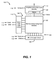
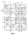
- the data storage cell 226 may be coupled to the first clamp transistor 218 via a selection transistor such as the first MUX transistor 224 to enable a current flow from the voltage supply 206 of the first amplifier 202 through the data storage cell 226, such as illustrated in FIG. 2 .
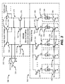
- one of the memory cells 326 may be coupled to the first clamp transistor 318 via a selection transistor such as a respective one of the MUX transistors 324 to enable a current flow from the voltage supply of the first amplifier stage 302 through the corresponding one of the memory cells 326, such as illustrated in FIG. 3 .
Landscapes
- Engineering & Computer Science (AREA)
- Computer Hardware Design (AREA)
- Mram Or Spin Memory Techniques (AREA)
- Hall/Mr Elements (AREA)
Claims (11)
- Eine Speichereinrichtung (100; 200; 300), die folgendes aufweist:eine Speicherzelle (226; 326), die ein widerstandsbasiertes Speicherelement (228; 328, 358, 388) enthält, dass an einen Zugriffstransistor (230; 330) gekoppelt ist, wobei der Zugriffstransistor (230; 330) eine erste Oxiddicke hat, um Betrieb der Speicherzelle (226; 326) an einer Betriebspannung zu ermöglichen;
undeinen ersten Verstärker, der zum Koppeln der Speicherzelle (226; 326) an eine Versorgungsspannung konfiguriert ist, die größer ist als eine Spannungsgrenze zum Erzeugen eines Datensignals basierend auf einen Strom durch die Speicherzelle (226; 326),
dadurch gekennzeichnet, dassder erste Verstärker (112; 202; 302) einen Klemmtransistor, auch Clamp Transistor, (120; 218; 318) enthält, der eine zweite Oxiddicke hat, die größer als die erste Oxiddicke ist, und wobei der Klemmtransistor (120; 218; 318) konfiguriert ist um zu verhindern, dass die Betriebspannung an der Speicherzelle (226; 326) die Spannungsgrenze überschreitet. - Speichereinrichtung (100; 200; 300) nach Anspruch 1, wobei der Klemmtransistor (120; 218; 318) konfiguriert ist, um mit einer Eingangs-Ausgangs-Versorgungsspannung, auch IO Versorgungsspannung, (IO = Input-Output), betrieben zu werden, und wobei der Zugriffstransistor (230; 330) konfiguriert ist, um mit einer Kernversorgungsspannung betrieben zu werden.
- Speichereinrichtung (100; 200; 300) nach Anspruch 2, wobei die Kernversorgungsspannung ungefähr 1 Volt ist und wobei die IO-Versorgungsspannung ungefähr 1,8 Volt ist.
- Speichereinrichtung (100; 200; 300) nach Anspruch 1, wobei die Speicherzelle (226; 326) eine Spin-Transfer Torque Magnetoresistive Random Access Memory Zelle, auch STT-MRAM Zelle ist.
- Speichereinrichtung (100; 200; 300) nach Anspruch 1, wobei der erste Verstärker (112; 202; 302) weiterhin konfiguriert ist, um mindestens eine Referenzzelle (256, 286; 356, 386) an die Versorgungsspannung zu koppeln, um ein Referenzsignal zu erzeugen, und die weiterhin Folgendes aufweist:einen zweiten Verstärker (312), der an den ersten Verstärker (112; 202; 302) gekoppelt ist und zum Bereitstellen eines Ausgangssignals basierend auf einer Differenz zwischen dem Datensignal und dem Referenzsignal konfiguriert ist, wobei der zweite Transistor (312) mindestens einen Transistor enthält, der die erste Oxiddicke hat und der an eine zweite Versorgungsspannung gekoppelt ist, welche die Spannungsgrenze nicht überschreitet.
- Speichereinrichtung (100; 200; 300) nach Anspruch 1, wobei der erste Verstärker (112; 202; 302) weiterhin folgendes aufweist:einen ersten Lasttransistor, auch Load Transistor, (214; 314), der an den Klemmtransistor (120; 218; 318) gekoppelt ist, um das Datensignal zu erzeugen;einen zweiten Lasttransistor (244; 344), der an einen zweiten Klemmtransistor (248; 348) gekoppelt ist; undeinen dritten Lasttransistor (274; 374), der an einen dritten Klemmtransistor (278; 378) gekoppelt ist, wobei der zweite Klemmtransistor und der dritte Klemmtransistor zum Koppeln an eine erste Referenzzelle (256, 286; 356, 386) und an eine zweite Referenzzelle (256, 286; 356, 386) konfiguriert sind, um ein Referenzsignal zu erzeugen.
- Ein Verfahren, das folgendes aufweist:Koppeln einer ersten Verstärkerstufe (112; 202; 302) an ein Speicherarray (102; 304), wobei die erste Verstärkerstufe (112; 202; 302) folgendes enthält: Transistoren, die eine Eingangs-Ausgangs- (IO) -Versorgungsspannungstoleranz haben und einen Klemmtransistor (120; 218; 318), und wobei das Speicherarray (102; 304) weiterhin folgendes enthält: Transistoren mit einer Kernversorgungsspannungtoleranz, die geringer als die IO Versorgungsspannungtoleranz ist, und widerstandsbasierte Speicherelemente (228; 328, 358, 388); undAnlegen einer Steuerspannung an den Klemmtransistor (120; 218; 318), der an das Speicherarray gekoppelt ist, um eine Speicherarrayspannung einzustellen, so dass die Speicherarrayspannung geringer als die Kernversorgungsspannungstoleranz ist.
- Verfahren nach Anspruch 7, das weiterhin folgendes aufweist:Ausführen einer Datenleseoperation an einer Datenspeicherzelle (226; 326) des Speicherarrays (102; 304), um ein Datensignal an der ersten Verstärkerstufe zu erzeugen; undVergleichen des Datensignals von der ersten Verstärkerstufe (112; 202; 302) mit einem Referenzsignal um eine Ausgangssignal an einer zweiten Verstärkerstufe (312) zu erzeugen, wobei die zweite Verstärkerstufe (312) Einrichtungen enthält, welche die Kernversorgungsspannungtoleranz haben.
- Verfahren nach Anspruch 8, dass weiterhin folgendes aufweist:Koppeln der Datenspeicherzelle (226; 326) an den Klemmtransistor (120; 218; 318) über einen Auswahltransistor, auch Selection Transistor, um einen Stromfluss von einer Versorgungsspannung der ersten Verstärkerstufe (112; 202; 302) durch die Datenspeicherzelle (226; 326) zu ermöglichen.
- Verfahren nach Anspruch 9, wobei der Auswahltransistor die Kernversorgungsspannungtoleranz hat.
- Verfahren nach Anspruch 9, wobei ein Erhöhen der Versorgungsspannung der ersten Verstärkerstufe (112; 202; 302) einen Lesemarge der Datenleseoperation erhöht.
Applications Claiming Priority (2)
| Application Number | Priority Date | Filing Date | Title |
|---|---|---|---|
| US12/206,933 US8228714B2 (en) | 2008-09-09 | 2008-09-09 | Memory device for resistance-based memory applications |
| PCT/US2009/055617 WO2010030531A1 (en) | 2008-09-09 | 2009-09-01 | Memory device for resistance-based memory applications |
Publications (2)
| Publication Number | Publication Date |
|---|---|
| EP2332142A1 EP2332142A1 (de) | 2011-06-15 |
| EP2332142B1 true EP2332142B1 (de) | 2013-07-10 |
Family
ID=41226077
Family Applications (1)
| Application Number | Title | Priority Date | Filing Date |
|---|---|---|---|
| EP09792136.5A Active EP2332142B1 (de) | 2008-09-09 | 2009-09-01 | Speichervorrichtung für widerstandsspeicheranwendungen |
Country Status (12)
| Country | Link |
|---|---|
| US (1) | US8228714B2 (de) |
| EP (1) | EP2332142B1 (de) |
| JP (2) | JP5265773B2 (de) |
| KR (1) | KR101305337B1 (de) |
| CN (1) | CN102150214B (de) |
| BR (1) | BRPI0918916B1 (de) |
| CA (1) | CA2735725C (de) |
| ES (1) | ES2424222T3 (de) |
| MX (1) | MX2011002566A (de) |
| RU (1) | RU2476940C2 (de) |
| TW (1) | TWI444998B (de) |
| WO (1) | WO2010030531A1 (de) |
Families Citing this family (11)
| Publication number | Priority date | Publication date | Assignee | Title |
|---|---|---|---|---|
| US8228714B2 (en) * | 2008-09-09 | 2012-07-24 | Qualcomm Incorporated | Memory device for resistance-based memory applications |
| KR101094944B1 (ko) * | 2009-12-24 | 2011-12-15 | 주식회사 하이닉스반도체 | 센싱 전압을 제어하는 비휘발성 반도체 집적 회로 |
| US8335101B2 (en) * | 2010-01-21 | 2012-12-18 | Qualcomm Incorporated | Resistance-based memory with reduced voltage input/output device |
| US8625338B2 (en) | 2010-04-07 | 2014-01-07 | Qualcomm Incorporated | Asymmetric write scheme for magnetic bit cell elements |
| US8254195B2 (en) * | 2010-06-01 | 2012-08-28 | Qualcomm Incorporated | High-speed sensing for resistive memories |
| US8446757B2 (en) | 2010-08-18 | 2013-05-21 | International Business Machines Corporation | Spin-torque transfer magneto-resistive memory architecture |
| US8531902B2 (en) * | 2011-06-30 | 2013-09-10 | Qualcomm Incorporated | Sensing circuit |
| US8693273B2 (en) * | 2012-01-06 | 2014-04-08 | Headway Technologies, Inc. | Reference averaging for MRAM sense amplifiers |
| US10205088B2 (en) * | 2016-10-27 | 2019-02-12 | Tdk Corporation | Magnetic memory |
| US10528862B1 (en) * | 2018-07-26 | 2020-01-07 | Macronix International Co., Ltd. | Neural network system and method for controlling the same |
| US20200098409A1 (en) * | 2018-09-24 | 2020-03-26 | Qualcomm Incorporated | Magnetic random access memory (mram) integration |
Family Cites Families (24)
| Publication number | Priority date | Publication date | Assignee | Title |
|---|---|---|---|---|
| JP2002100181A (ja) * | 2000-09-27 | 2002-04-05 | Nec Corp | 磁気ランダムアクセスメモリ |
| JP3856424B2 (ja) | 2000-12-25 | 2006-12-13 | 株式会社東芝 | 半導体記憶装置 |
| CN1305187C (zh) * | 2002-01-21 | 2007-03-14 | 松下电器产业株式会社 | 氮化物半导体激光元件及其制造方法 |
| JP2003223788A (ja) | 2002-01-29 | 2003-08-08 | Hitachi Ltd | 半導体集積回路装置 |
| US6600690B1 (en) * | 2002-06-28 | 2003-07-29 | Motorola, Inc. | Sense amplifier for a memory having at least two distinct resistance states |
| JP3821066B2 (ja) * | 2002-07-04 | 2006-09-13 | 日本電気株式会社 | 磁気ランダムアクセスメモリ |
| JP2004110992A (ja) * | 2002-09-20 | 2004-04-08 | Renesas Technology Corp | 薄膜磁性体記憶装置 |
| US6999345B1 (en) * | 2002-11-06 | 2006-02-14 | Halo Lsi, Inc. | Method of sense and program verify without a reference cell for non-volatile semiconductor memory |
| JP4331966B2 (ja) * | 2003-04-14 | 2009-09-16 | 株式会社ルネサステクノロジ | 半導体集積回路 |
| JP4407828B2 (ja) * | 2003-04-21 | 2010-02-03 | 日本電気株式会社 | データの読み出し方法が改善された磁気ランダムアクセスメモリ |
| JP4646636B2 (ja) * | 2004-02-20 | 2011-03-09 | ルネサスエレクトロニクス株式会社 | 半導体装置 |
| US7236418B2 (en) * | 2004-06-25 | 2007-06-26 | Qualcomm Incorporated | Reduced area, reduced programming voltage CMOS eFUSE-based scannable non-volatile memory bitcell |
| FR2878067B1 (fr) | 2004-11-17 | 2007-01-26 | St Microelectronics Sa | Dispositif de lecture faible tension notamment pour memoire mram |
| US7082061B2 (en) * | 2004-12-03 | 2006-07-25 | Macronix International Co., Ltd. | Memory array with low power bit line precharge |
| DE102005029872A1 (de) * | 2005-06-27 | 2007-04-19 | Infineon Technologies Ag | Speicherzelle, Lesevorrichtung für die Speicherzelle sowie Speicheranordnungen mit einer derartigen Speicherzelle und Lesevorrichtung |
| US20070015989A1 (en) * | 2005-07-01 | 2007-01-18 | Avantis Medical Systems, Inc. | Endoscope Image Recognition System and Method |
| US7272035B1 (en) | 2005-08-31 | 2007-09-18 | Grandis, Inc. | Current driven switching of magnetic storage cells utilizing spin transfer and magnetic memories using such cells |
| KR100764738B1 (ko) * | 2006-04-06 | 2007-10-09 | 삼성전자주식회사 | 향상된 신뢰성을 갖는 상변화 메모리 장치, 그것의 쓰기방법, 그리고 그것을 포함한 시스템 |
| US7345912B2 (en) * | 2006-06-01 | 2008-03-18 | Grandis, Inc. | Method and system for providing a magnetic memory structure utilizing spin transfer |
| WO2008050398A1 (en) * | 2006-10-24 | 2008-05-02 | Fujitsu Limited | Resistance change memory |
| US20080211541A1 (en) * | 2007-03-02 | 2008-09-04 | Texas Instruments Incorporated | Precision voltage level shifter based on thin gate oxide transistors |
| US7738306B2 (en) * | 2007-12-07 | 2010-06-15 | Etron Technology, Inc. | Method to improve the write speed for memory products |
| US8228714B2 (en) * | 2008-09-09 | 2012-07-24 | Qualcomm Incorporated | Memory device for resistance-based memory applications |
| US8335101B2 (en) * | 2010-01-21 | 2012-12-18 | Qualcomm Incorporated | Resistance-based memory with reduced voltage input/output device |
-
2008
- 2008-09-09 US US12/206,933 patent/US8228714B2/en active Active
-
2009
- 2009-09-01 BR BRPI0918916-5A patent/BRPI0918916B1/pt active IP Right Grant
- 2009-09-01 ES ES09792136T patent/ES2424222T3/es active Active
- 2009-09-01 RU RU2011113767/08A patent/RU2476940C2/ru not_active IP Right Cessation
- 2009-09-01 CA CA2735725A patent/CA2735725C/en not_active Expired - Fee Related
- 2009-09-01 CN CN200980135343.6A patent/CN102150214B/zh active Active
- 2009-09-01 KR KR1020117008148A patent/KR101305337B1/ko active Active
- 2009-09-01 JP JP2011526135A patent/JP5265773B2/ja active Active
- 2009-09-01 WO PCT/US2009/055617 patent/WO2010030531A1/en not_active Ceased
- 2009-09-01 MX MX2011002566A patent/MX2011002566A/es not_active Application Discontinuation
- 2009-09-01 EP EP09792136.5A patent/EP2332142B1/de active Active
- 2009-09-09 TW TW098130422A patent/TWI444998B/zh active
-
2013
- 2013-05-01 JP JP2013096313A patent/JP2013178869A/ja not_active Withdrawn
Also Published As
| Publication number | Publication date |
|---|---|
| CN102150214A (zh) | 2011-08-10 |
| RU2011113767A (ru) | 2012-10-20 |
| WO2010030531A1 (en) | 2010-03-18 |
| US8228714B2 (en) | 2012-07-24 |
| TWI444998B (zh) | 2014-07-11 |
| MX2011002566A (es) | 2011-04-07 |
| ES2424222T3 (es) | 2013-09-30 |
| BRPI0918916A2 (pt) | 2018-02-14 |
| EP2332142A1 (de) | 2011-06-15 |
| CN102150214B (zh) | 2014-05-07 |
| JP2013178869A (ja) | 2013-09-09 |
| RU2476940C2 (ru) | 2013-02-27 |
| JP2012502401A (ja) | 2012-01-26 |
| US20100061144A1 (en) | 2010-03-11 |
| KR20110053274A (ko) | 2011-05-19 |
| BRPI0918916B1 (pt) | 2020-07-21 |
| JP5265773B2 (ja) | 2013-08-14 |
| KR101305337B1 (ko) | 2013-09-06 |
| CA2735725A1 (en) | 2010-03-18 |
| TW201023180A (en) | 2010-06-16 |
| CA2735725C (en) | 2014-06-03 |
Similar Documents
| Publication | Publication Date | Title |
|---|---|---|
| EP2332142B1 (de) | Speichervorrichtung für widerstandsspeicheranwendungen | |
| US7272034B1 (en) | Current driven switching of magnetic storage cells utilizing spin transfer and magnetic memories using such cells | |
| US7791930B2 (en) | Magnetoresistive random access memory | |
| US10157655B2 (en) | Memory device | |
| CN102148055B (zh) | 使用自旋mos晶体管的非易失性存储器电路 | |
| JP2004103104A (ja) | 薄膜磁性体記憶装置 | |
| US10431277B2 (en) | Memory device | |
| US10269403B2 (en) | Semiconductor storage device | |
| US9472256B1 (en) | Magnetic memory having two transistors and two magnetic tunnel junctions per memory cell | |
| US20070258282A1 (en) | Magnetic memory device and method of writing data in the same | |
| Chang et al. | A low-voltage bulk-drain-driven read scheme for sub-0.5 V 4 Mb 65 nm logic-process compatible embedded resistive RAM (ReRAM) macro | |
| US7002865B2 (en) | Nonvolatile semiconductor memory device | |
| JP5135609B2 (ja) | 半導体装置 | |
| CN113129953B (zh) | 磁性随机存储器的读电路 | |
| JP2012190515A (ja) | 半導体記憶装置 | |
| JP2010027178A (ja) | 記憶装置 | |
| JP2004348826A (ja) | 磁気記憶装置 | |
| JP4322048B2 (ja) | 半導体記憶装置 | |
| US11309025B2 (en) | Semiconductor circuit and semiconductor circuit system to suppress disturbance in the semiconductor circuit | |
| JP2004171625A (ja) | 不揮発性記憶装置 | |
| KR101704929B1 (ko) | 센싱 마진을 향상시키는 메모리 셀 읽기 회로 | |
| US20250111869A1 (en) | Memory devices with dual-side access circuits and methods for operating the same | |
| US10832752B2 (en) | Memory write and read assistance using negative differential resistance devices | |
| Takemura et al. | Highly-scalable disruptive reading and restoring scheme for Gb-scale SPRAM and beyond | |
| Huang et al. | High-voltage tolerant circuit design for fully CMOS compatible multiple-time programmable memories |
Legal Events
| Date | Code | Title | Description |
|---|---|---|---|
| PUAI | Public reference made under article 153(3) epc to a published international application that has entered the european phase |
Free format text: ORIGINAL CODE: 0009012 |
|
| 17P | Request for examination filed |
Effective date: 20110407 |
|
| AK | Designated contracting states |
Kind code of ref document: A1 Designated state(s): AT BE BG CH CY CZ DE DK EE ES FI FR GB GR HR HU IE IS IT LI LT LU LV MC MK MT NL NO PL PT RO SE SI SK SM TR |
|
| AX | Request for extension of the european patent |
Extension state: AL BA RS |
|
| DAX | Request for extension of the european patent (deleted) | ||
| 17Q | First examination report despatched |
Effective date: 20121120 |
|
| GRAP | Despatch of communication of intention to grant a patent |
Free format text: ORIGINAL CODE: EPIDOSNIGR1 |
|
| GRAS | Grant fee paid |
Free format text: ORIGINAL CODE: EPIDOSNIGR3 |
|
| GRAA | (expected) grant |
Free format text: ORIGINAL CODE: 0009210 |
|
| AK | Designated contracting states |
Kind code of ref document: B1 Designated state(s): AT BE BG CH CY CZ DE DK EE ES FI FR GB GR HR HU IE IS IT LI LT LU LV MC MK MT NL NO PL PT RO SE SI SK SM TR |
|
| REG | Reference to a national code |
Ref country code: GB Ref legal event code: FG4D |
|
| REG | Reference to a national code |
Ref country code: AT Ref legal event code: REF Ref document number: 621366 Country of ref document: AT Kind code of ref document: T Effective date: 20130715 Ref country code: CH Ref legal event code: EP |
|
| REG | Reference to a national code |
Ref country code: IE Ref legal event code: FG4D |
|
| REG | Reference to a national code |
Ref country code: DE Ref legal event code: R096 Ref document number: 602009017108 Country of ref document: DE Effective date: 20130912 |
|
| REG | Reference to a national code |
Ref country code: ES Ref legal event code: FG2A Ref document number: 2424222 Country of ref document: ES Kind code of ref document: T3 Effective date: 20130930 |
|
| PG25 | Lapsed in a contracting state [announced via postgrant information from national office to epo] |
Ref country code: SI Free format text: LAPSE BECAUSE OF FAILURE TO SUBMIT A TRANSLATION OF THE DESCRIPTION OR TO PAY THE FEE WITHIN THE PRESCRIBED TIME-LIMIT Effective date: 20130710 |
|
| REG | Reference to a national code |
Ref country code: NL Ref legal event code: T3 |
|
| REG | Reference to a national code |
Ref country code: AT Ref legal event code: MK05 Ref document number: 621366 Country of ref document: AT Kind code of ref document: T Effective date: 20130710 |
|
| REG | Reference to a national code |
Ref country code: LT Ref legal event code: MG4D |
|
| PG25 | Lapsed in a contracting state [announced via postgrant information from national office to epo] |
Ref country code: PT Free format text: LAPSE BECAUSE OF FAILURE TO SUBMIT A TRANSLATION OF THE DESCRIPTION OR TO PAY THE FEE WITHIN THE PRESCRIBED TIME-LIMIT Effective date: 20131111 Ref country code: CY Free format text: LAPSE BECAUSE OF FAILURE TO SUBMIT A TRANSLATION OF THE DESCRIPTION OR TO PAY THE FEE WITHIN THE PRESCRIBED TIME-LIMIT Effective date: 20130717 Ref country code: SE Free format text: LAPSE BECAUSE OF FAILURE TO SUBMIT A TRANSLATION OF THE DESCRIPTION OR TO PAY THE FEE WITHIN THE PRESCRIBED TIME-LIMIT Effective date: 20130710 Ref country code: NO Free format text: LAPSE BECAUSE OF FAILURE TO SUBMIT A TRANSLATION OF THE DESCRIPTION OR TO PAY THE FEE WITHIN THE PRESCRIBED TIME-LIMIT Effective date: 20131010 Ref country code: AT Free format text: LAPSE BECAUSE OF FAILURE TO SUBMIT A TRANSLATION OF THE DESCRIPTION OR TO PAY THE FEE WITHIN THE PRESCRIBED TIME-LIMIT Effective date: 20130710 Ref country code: IS Free format text: LAPSE BECAUSE OF FAILURE TO SUBMIT A TRANSLATION OF THE DESCRIPTION OR TO PAY THE FEE WITHIN THE PRESCRIBED TIME-LIMIT Effective date: 20131110 Ref country code: HR Free format text: LAPSE BECAUSE OF FAILURE TO SUBMIT A TRANSLATION OF THE DESCRIPTION OR TO PAY THE FEE WITHIN THE PRESCRIBED TIME-LIMIT Effective date: 20130710 Ref country code: LT Free format text: LAPSE BECAUSE OF FAILURE TO SUBMIT A TRANSLATION OF THE DESCRIPTION OR TO PAY THE FEE WITHIN THE PRESCRIBED TIME-LIMIT Effective date: 20130710 Ref country code: BE Free format text: LAPSE BECAUSE OF FAILURE TO SUBMIT A TRANSLATION OF THE DESCRIPTION OR TO PAY THE FEE WITHIN THE PRESCRIBED TIME-LIMIT Effective date: 20130710 |
|
| PG25 | Lapsed in a contracting state [announced via postgrant information from national office to epo] |
Ref country code: GR Free format text: LAPSE BECAUSE OF FAILURE TO SUBMIT A TRANSLATION OF THE DESCRIPTION OR TO PAY THE FEE WITHIN THE PRESCRIBED TIME-LIMIT Effective date: 20131011 Ref country code: LV Free format text: LAPSE BECAUSE OF FAILURE TO SUBMIT A TRANSLATION OF THE DESCRIPTION OR TO PAY THE FEE WITHIN THE PRESCRIBED TIME-LIMIT Effective date: 20130710 Ref country code: FI Free format text: LAPSE BECAUSE OF FAILURE TO SUBMIT A TRANSLATION OF THE DESCRIPTION OR TO PAY THE FEE WITHIN THE PRESCRIBED TIME-LIMIT Effective date: 20130710 Ref country code: PL Free format text: LAPSE BECAUSE OF FAILURE TO SUBMIT A TRANSLATION OF THE DESCRIPTION OR TO PAY THE FEE WITHIN THE PRESCRIBED TIME-LIMIT Effective date: 20130710 |
|
| PG25 | Lapsed in a contracting state [announced via postgrant information from national office to epo] |
Ref country code: CY Free format text: LAPSE BECAUSE OF FAILURE TO SUBMIT A TRANSLATION OF THE DESCRIPTION OR TO PAY THE FEE WITHIN THE PRESCRIBED TIME-LIMIT Effective date: 20130710 |
|
| PG25 | Lapsed in a contracting state [announced via postgrant information from national office to epo] |
Ref country code: CZ Free format text: LAPSE BECAUSE OF FAILURE TO SUBMIT A TRANSLATION OF THE DESCRIPTION OR TO PAY THE FEE WITHIN THE PRESCRIBED TIME-LIMIT Effective date: 20130710 Ref country code: RO Free format text: LAPSE BECAUSE OF FAILURE TO SUBMIT A TRANSLATION OF THE DESCRIPTION OR TO PAY THE FEE WITHIN THE PRESCRIBED TIME-LIMIT Effective date: 20130710 Ref country code: MC Free format text: LAPSE BECAUSE OF FAILURE TO SUBMIT A TRANSLATION OF THE DESCRIPTION OR TO PAY THE FEE WITHIN THE PRESCRIBED TIME-LIMIT Effective date: 20130710 Ref country code: DK Free format text: LAPSE BECAUSE OF FAILURE TO SUBMIT A TRANSLATION OF THE DESCRIPTION OR TO PAY THE FEE WITHIN THE PRESCRIBED TIME-LIMIT Effective date: 20130710 Ref country code: EE Free format text: LAPSE BECAUSE OF FAILURE TO SUBMIT A TRANSLATION OF THE DESCRIPTION OR TO PAY THE FEE WITHIN THE PRESCRIBED TIME-LIMIT Effective date: 20130710 Ref country code: SK Free format text: LAPSE BECAUSE OF FAILURE TO SUBMIT A TRANSLATION OF THE DESCRIPTION OR TO PAY THE FEE WITHIN THE PRESCRIBED TIME-LIMIT Effective date: 20130710 |
|
| REG | Reference to a national code |
Ref country code: CH Ref legal event code: PL |
|
| PLBE | No opposition filed within time limit |
Free format text: ORIGINAL CODE: 0009261 |
|
| STAA | Information on the status of an ep patent application or granted ep patent |
Free format text: STATUS: NO OPPOSITION FILED WITHIN TIME LIMIT |
|
| 26N | No opposition filed |
Effective date: 20140411 |
|
| REG | Reference to a national code |
Ref country code: IE Ref legal event code: MM4A |
|
| REG | Reference to a national code |
Ref country code: DE Ref legal event code: R097 Ref document number: 602009017108 Country of ref document: DE Effective date: 20140411 |
|
| PG25 | Lapsed in a contracting state [announced via postgrant information from national office to epo] |
Ref country code: IE Free format text: LAPSE BECAUSE OF NON-PAYMENT OF DUE FEES Effective date: 20130901 Ref country code: LI Free format text: LAPSE BECAUSE OF NON-PAYMENT OF DUE FEES Effective date: 20130930 Ref country code: CH Free format text: LAPSE BECAUSE OF NON-PAYMENT OF DUE FEES Effective date: 20130930 |
|
| PG25 | Lapsed in a contracting state [announced via postgrant information from national office to epo] |
Ref country code: SM Free format text: LAPSE BECAUSE OF FAILURE TO SUBMIT A TRANSLATION OF THE DESCRIPTION OR TO PAY THE FEE WITHIN THE PRESCRIBED TIME-LIMIT Effective date: 20130710 |
|
| PG25 | Lapsed in a contracting state [announced via postgrant information from national office to epo] |
Ref country code: TR Free format text: LAPSE BECAUSE OF FAILURE TO SUBMIT A TRANSLATION OF THE DESCRIPTION OR TO PAY THE FEE WITHIN THE PRESCRIBED TIME-LIMIT Effective date: 20130710 Ref country code: MT Free format text: LAPSE BECAUSE OF FAILURE TO SUBMIT A TRANSLATION OF THE DESCRIPTION OR TO PAY THE FEE WITHIN THE PRESCRIBED TIME-LIMIT Effective date: 20130710 |
|
| PG25 | Lapsed in a contracting state [announced via postgrant information from national office to epo] |
Ref country code: MK Free format text: LAPSE BECAUSE OF FAILURE TO SUBMIT A TRANSLATION OF THE DESCRIPTION OR TO PAY THE FEE WITHIN THE PRESCRIBED TIME-LIMIT Effective date: 20130710 Ref country code: BG Free format text: LAPSE BECAUSE OF FAILURE TO SUBMIT A TRANSLATION OF THE DESCRIPTION OR TO PAY THE FEE WITHIN THE PRESCRIBED TIME-LIMIT Effective date: 20130710 Ref country code: LU Free format text: LAPSE BECAUSE OF NON-PAYMENT OF DUE FEES Effective date: 20130901 Ref country code: HU Free format text: LAPSE BECAUSE OF FAILURE TO SUBMIT A TRANSLATION OF THE DESCRIPTION OR TO PAY THE FEE WITHIN THE PRESCRIBED TIME-LIMIT; INVALID AB INITIO Effective date: 20090901 |
|
| REG | Reference to a national code |
Ref country code: FR Ref legal event code: PLFP Year of fee payment: 8 |
|
| REG | Reference to a national code |
Ref country code: FR Ref legal event code: PLFP Year of fee payment: 9 |
|
| REG | Reference to a national code |
Ref country code: FR Ref legal event code: PLFP Year of fee payment: 10 |
|
| PGFP | Annual fee paid to national office [announced via postgrant information from national office to epo] |
Ref country code: NL Payment date: 20250812 Year of fee payment: 17 |
|
| PGFP | Annual fee paid to national office [announced via postgrant information from national office to epo] |
Ref country code: DE Payment date: 20250808 Year of fee payment: 17 |
|
| PGFP | Annual fee paid to national office [announced via postgrant information from national office to epo] |
Ref country code: IT Payment date: 20250911 Year of fee payment: 17 |
|
| PGFP | Annual fee paid to national office [announced via postgrant information from national office to epo] |
Ref country code: GB Payment date: 20250814 Year of fee payment: 17 |
|
| PGFP | Annual fee paid to national office [announced via postgrant information from national office to epo] |
Ref country code: FR Payment date: 20250808 Year of fee payment: 17 |
|
| PGFP | Annual fee paid to national office [announced via postgrant information from national office to epo] |
Ref country code: ES Payment date: 20251003 Year of fee payment: 17 |