EP2332142B1 - Memory device for resistance-based memory applications - Google Patents
Memory device for resistance-based memory applications Download PDFInfo
- Publication number
- EP2332142B1 EP2332142B1 EP09792136.5A EP09792136A EP2332142B1 EP 2332142 B1 EP2332142 B1 EP 2332142B1 EP 09792136 A EP09792136 A EP 09792136A EP 2332142 B1 EP2332142 B1 EP 2332142B1
- Authority
- EP
- European Patent Office
- Prior art keywords
- transistor
- memory
- coupled
- voltage
- supply voltage
- Prior art date
- Legal status (The legal status is an assumption and is not a legal conclusion. Google has not performed a legal analysis and makes no representation as to the accuracy of the status listed.)
- Active
Links
Images

Classifications
-
- G—PHYSICS
- G11—INFORMATION STORAGE
- G11C—STATIC STORES
- G11C11/00—Digital stores characterised by the use of particular electric or magnetic storage elements; Storage elements therefor
- G11C11/02—Digital stores characterised by the use of particular electric or magnetic storage elements; Storage elements therefor using magnetic elements
- G11C11/14—Digital stores characterised by the use of particular electric or magnetic storage elements; Storage elements therefor using magnetic elements using thin-film elements
- G11C11/15—Digital stores characterised by the use of particular electric or magnetic storage elements; Storage elements therefor using magnetic elements using thin-film elements using multiple magnetic layers
-
- G—PHYSICS
- G11—INFORMATION STORAGE
- G11C—STATIC STORES
- G11C11/00—Digital stores characterised by the use of particular electric or magnetic storage elements; Storage elements therefor
- G11C11/02—Digital stores characterised by the use of particular electric or magnetic storage elements; Storage elements therefor using magnetic elements
- G11C11/16—Digital stores characterised by the use of particular electric or magnetic storage elements; Storage elements therefor using magnetic elements using elements in which the storage effect is based on magnetic spin effect
- G11C11/165—Auxiliary circuits
- G11C11/1673—Reading or sensing circuits or methods
-
- G—PHYSICS
- G11—INFORMATION STORAGE
- G11C—STATIC STORES
- G11C16/00—Erasable programmable read-only memories
- G11C16/02—Erasable programmable read-only memories electrically programmable
- G11C16/06—Auxiliary circuits, e.g. for writing into memory
-
- G—PHYSICS
- G11—INFORMATION STORAGE
- G11C—STATIC STORES
- G11C16/00—Erasable programmable read-only memories
- G11C16/02—Erasable programmable read-only memories electrically programmable
- G11C16/06—Auxiliary circuits, e.g. for writing into memory
- G11C16/26—Sensing or reading circuits; Data output circuits
Definitions
- US2008/137430 relates to a circuit including first and second transistors for controlling the bit line and a reference line, respectively, a reference transistor connected to the second control transistor and a write transistor of the reference current connected to the first control transistor, for comparing the current of the bit line and the reference current.
- a first intermediate transistor is connected to the write transistor parallel to the first control transistor, and a second intermediate transistor is connected between the gate and the drain of the reference transistor parallel to the second control transistor.
- Polarization transistors are connected in series, respectively, to the intermediate transistors so as to superimpose a current over the reference current.
- the data storage cell may be coupled to the first clamp transistor via a selection transistor to enable a current flow from a voltage supply of the first amplifier through the data storage cell.
- the data storage cell 226 may be coupled to the first clamp transistor 218 via a selection transistor such as the first MUX transistor 224 to enable a current flow from the voltage supply 206 of the first amplifier 202 through the data storage cell 226, such as illustrated in FIG. 2 .
- one of the memory cells 326 may be coupled to the first clamp transistor 318 via a selection transistor such as a respective one of the MUX transistors 324 to enable a current flow from the voltage supply of the first amplifier stage 302 through the corresponding one of the memory cells 326, such as illustrated in FIG. 3 .
Landscapes
- Engineering & Computer Science (AREA)
- Computer Hardware Design (AREA)
- Mram Or Spin Memory Techniques (AREA)
- Hall/Mr Elements (AREA)
Description
- The present disclosure is generally directed to a memory device including an amplifier and a memory cell including a resistance-based memory element.
- Advances in non-volatile memory technology include resistance-based memory technologies, such as Magnetic Random Access Memory (MRAM). MRAM technology is an emerging non-volatile memory technology that employs ferromagnetic-based Magnetic Tunnel Junctions (MTJs) as the basic memory elements. A commonly used array architecture for MRAMs is the one-transistor, one-MTJ (1T1MTJ) architecture. As the name suggests, each bit cell in this architecture consists of an MTJ connected in series with an NMOS access transistor. In order to leverage the increased density and area reduction advantages associated with scaling down MOS technologies, it is desirable to use core transistors within the MRAM bit cell. However, while scaling down MOS technology into the deep submicron regime yields area and density benefits to the MRAM bit cells, using these deep submicron devices in the MRAM sense amplifier degrades the read performance (the output swing) of the MRAM sense amplifier due to operating voltage limitations of these deep submicron devices.
- Conventional MRAM sense amplifier designs for the 1T1MTJ architecture use core transistors. However, due to breakdown and reliability considerations, the supply voltage for the core transistors is typically limited to about 1 volt (V) for leading-edge deep submicron technologies. The following devices are stacked between the supply rails in conventional MRAM sense amplifier designs for the 1T1MTJ architecture: the bit cell comprising an access transistor and an MTJ device, a mux transistor, a clamp transistor, and a PMOS load transistor. The access and mux transistors should be operated as switches (in the linear region), while the clamp and PMOS load transistors should remain in saturation for the sense amplifier to exhibit reasonable gain. However, the low supply voltage requirement that comes from using core devices in the sense amplifier coupled with the transistor threshold voltage being a significant fraction of this supply voltage can make it difficult to keep the clamp and PMOS load transistors in saturation, which in turn, degrades the gain and results in a sub-optimal signal swing at the sense amplifier output.
-
US2008/137430 relates to a circuit including first and second transistors for controlling the bit line and a reference line, respectively, a reference transistor connected to the second control transistor and a write transistor of the reference current connected to the first control transistor, for comparing the current of the bit line and the reference current. A first intermediate transistor is connected to the write transistor parallel to the first control transistor, and a second intermediate transistor is connected between the gate and the drain of the reference transistor parallel to the second control transistor. Polarization transistors are connected in series, respectively, to the intermediate transistors so as to superimpose a current over the reference current. -
US7272035 discusses a system in which each of a plurality of magnetic storage cells includes a magnetic element and a selection transistor. The magnetic element may be programmed using spin transfer induced switching by a write current driven through the magnetic element. The plurality of magnetic storage cells are grouped in pairs. The source of the selection transistor for one magnetic storage cell of a pair shares the source with the selection transistor for another magnetic storage cell of the pair. - The semiconductor device of
US2004/125683 comprises a cell array of memory cells each including a cell transistor and a capacitor, word lines and bit line pairs. A control circuit controls the memory circuit to set the bit lines to a high level to write "1" data into the memory cells regardless of a logic level of data to be written, in a state where a potential of a gate of the cell transistor of each memory cell is raised from a first potential of a standby time to a second potential of an active time, and thereafter to set the bit lines to a low level to write "0" data into the memory cells with "0" data to be written, in a state where the potential of the gate of the cell transistor is changed to a third potential higher than the first potential and lower than the second potential. - In a particular embodiment, a memory device is disclosed that includes a memory cell including a resistance-based memory element coupled to an access transistor. The access transistor has a first oxide thickness to enable operation of the memory cell at an operating voltage. The memory device also includes a first amplifier configured to couple the memory cell to a supply voltage that is greater than a voltage limit to generate a data signal based on a current through the memory cell. The first amplifier includes a clamp transistor that has a second oxide thickness that is greater than the first oxide thickness. The clamp transistor is configured to prevent the operating voltage at the memory cell from exceeding the voltage limit.
- In another embodiment, a memory device is disclosed that includes a data read path including a first load device coupled to a data storage cell via a first clamp transistor. The first load device has a first device configuration to operate at a first supply voltage. The data storage cell includes an access transistor having a second device configuration to operate at a voltage not to exceed a voltage limit that is less than the first supply voltage. A control terminal of the clamp transistor is biased to prevent the voltage at the data storage cell from exceeding the voltage limit.
- In another embodiment, a method is disclosed that includes coupling a first amplifier stage to a memory array. The first amplifier stage includes transistors having an input-output (IO) supply voltage tolerance. The memory array including transistors having a core supply voltage tolerance that is less than the IO supply voltage tolerance. The method includes applying a control voltage at a clamp transistor coupled to the memory array to set a memory array voltage, such that the memory array voltage is less than the core supply voltage tolerance.
- One particular advantage provided by the disclosed embodiments is an improvement in the read performance of the MRAM sense amplifier because the higher supply voltage enables a greater output swing to distinguish logical values during read operations.
- Other aspects, advantages, and features of the present disclosure will become apparent after review of the entire application, including the following sections: Brief Description of the Drawings, Detailed Description, and the Claims.
-
FIG. 1 is a diagram of a particular illustrative embodiment of a memory device with an amplifier using a first type of device and a memory array using a second type of device; -
FIG. 2 is a diagram of a second illustrative embodiment of a memory device with an amplifier using a first type of device and a memory array using a second type of device; -
FIG. 3 is a diagram of a third illustrative embodiment of a memory device with an amplifier using a first type of device and a memory array using a second type of device; and -
FIG. 4 is a flow diagram of a particular illustrative embodiment of a method of operating a memory device with an amplifier using a first type of device and a memory array using a second type of device. - Referring to
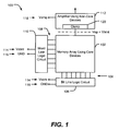
FIG. 1 , a diagram of a particular illustrative embodiment of a memory device with an amplifier using a first type of device and a memory array using a second type of device is depicted and generally designated 100. Thememory device 100 may include amemory array 102 using core devices. In a particular embodiment, the core devices may operate at core supply voltages Vcore of up to about 1 volt (V). Thememory array 102 may be coupled bybit lines 104 to a bitline logic circuit 106. Thememory array 102 may be coupled byword lines 108 to a wordline logic circuit 110. The bitline logic circuit 106 and the wordline logic circuit 110 may be coupled to a core supply voltage Vcore, as indicated at 114, and to ground, as indicated at 116. Thememory array 102 may also be coupled to anamplifier 112 that uses non-core devices. In a particular embodiment, the non-core devices may operate at input-output (IO) supply voltages Vamp of up to about 1.8V. Theamplifier 112 may be coupled to an IO supply voltage Vamp, as indicated at 118. Theamplifier 112 may include aclamp 120 coupled to thememory array 102 to keep an operating voltage Vop supplied to thememory array 102 by theamplifier 112 below a voltage limit Vlimit. - By employing a higher supply voltage Vamp and high-voltage-tolerant input-output (IO) devices for transistors in the
sense amplifier 112 while continuing to use area-efficient core devices in thememory array 102, for example, for MRAM bit cell transistors, such as access transistors and MUX transistors, read performance may be improved while maintaining a high array density. Since high-voltage-tolerant IO devices use a thicker gate oxide, their minimum feature size is also higher than that of core devices, which implies a higher area impact. As illustrated, thesystem 100 provides an improvement in the read performance (the output swing) of theMRAM sense amplifier 112 without much of an area penalty for thecomplete memory device 100 because (1) the higher supply voltage results in a greater output swing, thus, considerably improving the read performance, and (2) high-voltage-tolerant IO devices may be used only in thesense amplifier 112, while the MRAM bit cells that constitute a much larger portion of thememory device 100 area use high-density core devices. Since the number ofsense amplifiers 112 on a memory chip is far less than the number of bit cells, the area penalty that comes from using high-voltage-tolerant IO devices for the clamp and PMOS load transistors in thesense amplifier 112 may be minor compared to the significantly improved read performance that is associated with the use of the higher supply voltage. - Referring to
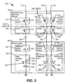
FIG. 2 , a diagram of a second illustrative embodiment of a memory device with an amplifier using a first type of device and a memory array using a second type of device is depicted and generally designated 200. In a particular embodiment, thememory device 200 operates substantially similarly to thememory device 100 illustrated inFIG. 1 . Thememory device 200 may include a memory (or data storage)cell 226 that may include a resistance-basedmemory element 228 coupled to anaccess transistor 230. Theaccess transistor 230 may have a first oxide thickness to enable operation of thememory cell 226 at an operating voltage Vop. In a particular embodiment, thememory cell 226 may be a spin-transfer torque magnetoresistive random access memory (STT-MRAM) cell. Thememory cell 226 may be included in amemory array 204. Thememory device 200 may also include afirst amplifier 202 configured to couple thememory cell 226 to a supply voltage Vamp at asupply terminal 206, where the supply voltage Vamp is greater than a voltage limit Vlimit, to generate a data signal based on a current through thememory cell 226. Thefirst amplifier 202 may include afirst clamp transistor 218 that has a second oxide thickness that is greater than the first oxide thickness of theaccess transistor 230. Theclamp transistor 218 may be configured to prevent the operating voltage Vop at thememory cell 226 from exceeding the voltage limit Vlimit. By providing an appropriate clamp control voltage Vclamp at acontrol terminal 208 to protect thememory array 204 from voltages exceeding Vlimit, thememory array 204 may use smaller devices for higher density and smaller sizes. In addition, thefirst amplifier 202 may use more robust devices to enhance operation using a larger supply voltage Vamp. - In a particular embodiment, the
access transistor 230 may have a core device configuration and thefirst clamp transistor 218 may have an input-output (IO) device configuration. In these particular embodiments, thefirst clamp transistor 218 may be configured to operate at an input-output (IO) supply voltage, Vamp, and theaccess transistor 230 may be configured to operate at a core supply voltage, Vcore. In these particular embodiments, the core supply voltage Vcore may be approximately IV, and the IO supply voltage Vamp may be approximately 1.8V. In a particular embodiment, theaccess transistor 230 may have the core device configuration with the first oxide thickness in a range from about 1nm to about 3nm. In these particular embodiments, thefirst clamp transistor 218 may have the input-output (IO) device configuration with the second oxide thickness in a range from about 3.5nm to about 10nm. - A data read
path 210 may include afirst load device 212 that may include afirst load transistor 214. In a particular embodiment, thefirst load transistor 214 may be a PMOS load transistor. Thefirst load device 212 may be coupled to afirst clamp device 216 that may include thefirst clamp transistor 218, where thefirst load transistor 214 may be coupled to thefirst clamp transistor 218. Thefirst clamp transistor 218 may be coupled to thecontrol terminal 208 that may be biased with the clamp voltage Vclamp. Thefirst clamp device 216 may be coupled through afirst node 220 to a firstselection switch device 222 that may include afirst MUX transistor 224, where thefirst clamp transistor 218 may be coupled to thefirst MUX transistor 224. The firstselection switch device 222 may be included in thememory array 204. The firstselection switch device 222 may be coupled to thememory cell 226, where thefirst MUX transistor 224 may be coupled to theaccess transistor 230 via the resistance-basedmemory element 228 having a resistance Rd. In a particular embodiment, the resistance-basedmemory element 228 may include a magnetic tunnel junction (MTJ) that may include areference layer 232, atunneling layer 234, and afree layer 236. Theaccess transistor 230 may be coupled to ground. - A
first reference path 240 may include asecond load device 242 that may include asecond load transistor 244. In a particular embodiment, thesecond load transistor 244 may be a PMOS load transistor. Thesecond load device 242 may be coupled to asecond clamp device 246 that may include asecond clamp transistor 248, where thesecond load transistor 244 may be coupled to thesecond clamp transistor 248. Thesecond clamp transistor 248 may be coupled to thecontrol terminal 208 that may be biased with the clamp voltage Vclamp. Thesecond clamp device 246 may be coupled through asecond node 250 to a secondselection switch device 252 that may include asecond MUX transistor 254, where thesecond clamp transistor 248 may be coupled to thesecond MUX transistor 254. The secondselection switch device 252 may be included in thememory array 204. The secondselection switch device 252 may be coupled to afirst reference cell 256, where thesecond MUX transistor 254 may be coupled to a firstreference access transistor 260 via a first resistance-basedreference element 258 having a resistance R1. In a particular embodiment, the resistance-basedmemory element 258 may include a magnetic tunnel junction (MTJ). The firstreference access transistor 260 may be coupled to ground. - A
second reference path 270 may include athird load device 272 that may include athird load transistor 274. In a particular embodiment, thethird load transistor 274 may be a PMOS load transistor. Thethird load device 272 may be coupled to athird clamp device 276 that may include athird clamp transistor 278, where thethird load transistor 274 may be coupled to thethird clamp transistor 278. Thethird clamp transistor 278 may be coupled to thecontrol terminal 208 that may be biased with the clamp voltage Vclamp. Thethird clamp device 276 may be coupled through asecond node 280 to a thirdselection switch device 282 that may include athird MUX transistor 284, where thethird clamp transistor 278 may be coupled to thethird MUX transistor 284. The thirdselection switch device 282 may be included in thememory array 204. The thirdselection switch device 282 may be coupled to asecond reference cell 286, where thethird MUX transistor 284 may be coupled to a secondreference access transistor 290 via a second resistance-basedreference element 288 having a resistance R0. In a particular embodiment, the resistance-basedmemory element 288 may include a magnetic tunnel junction (MTJ). The secondreference access transistor 290 may be coupled to ground. - The
first amplifier 202 may include thefirst load transistor 214 coupled to thefirst clamp transistor 218 to generate the data signal. Thefirst amplifier 202 may include thesecond load transistor 244 coupled to thesecond clamp transistor 248 and thethird load transistor 274 coupled to thethird clamp transistor 278. Thesecond clamp transistor 248 and thethird clamp transistor 278 may be configured to couple to thefirst reference cell 256 and to thesecond reference cell 286, respectively, to generate a reference signal. Thefirst clamp transistor 218, thesecond clamp transistor 248, thethird clamp transistor 278, thefirst load transistor 214, thesecond load transistor 244, and thethird load transistor 274 may have an input-output (IO) device configuration. At least onetransistor memory cell 226, thefirst reference cell 256, and thesecond reference cell 286 may have a core device configuration. In a particular embodiment, thefirst MUX transistor 224, thesecond MUX transistor 254, and thethird MUX transistor 284 may have the core device configuration. - As described above, the data read
path 210 may include thefirst load device 212 coupled to thedata storage cell 226 via thefirst clamp transistor 218. Thefirst load device 212 may have a first device configuration to operate at a first supply voltage Vamp supplied at thesupply terminal 206. In a particular embodiment, the first device configuration may be a non-core device configuration. In these particular embodiments, the first device configuration may be an input-output (IO) device configuration. Thedata storage cell 226 may include theaccess transistor 230 that may have a second device configuration to operate at an operating voltage Vop, at thenode 220, that is not to exceed a voltage limit Vlimit that is less than the first supply voltage Vamp. In a particular embodiment, the second device configuration may be a core device configuration. In these particular embodiments, the core device configuration may have a smaller physical dimension than the non-core configuration. Thecontrol terminal 208 of thefirst clamp transistor 218 may be biased to prevent the voltage Vop at thedata storage cell 226 from exceeding the voltage limit Vlimit. In a particular embodiment, the voltage limit Vlimit may be approximately 1V. - As described above, the
first reference path 240 may include thesecond load device 242 coupled to thefirst reference cell 256 and thesecond reference path 270 may include thethird load device 272 coupled to thesecond reference cell 286. Thesecond load device 242 and thethird load device 272 may have the first device configuration. Thefirst reference cell 256 and thesecond reference cell 286 each may include at least onetransistor second clamp transistor 248 may prevent a second voltage at thefirst reference cell 256 from exceeding the voltage limit Vlimit. Thethird clamp transistor 278 may prevent a third voltage at thesecond reference cell 286 from exceeding the voltage limit Vlimit. The firstselection switch device 222 in the data readpath 210 may selectively couple thedata storage cell 226 to thefirst clamp transistor 218. The secondselection switch device 252 in thefirst reference path 240 may selectively couple thefirst reference cell 256 to thesecond clamp transistor 248. The thirdselection switch device 282 in thesecond reference path 270 may selectively couple thesecond reference cell 286 to thethird clamp transistor 278. Each of the firstselection switch device 222, the secondselection switch device 252, and the thirdselection switch device 282 may have the second device configuration. - Referring to
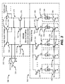
FIG. 3 , a diagram of a third illustrative embodiment of a memory device with an amplifier using a first type of device and a memory array using a second type of device is depicted and generally designated 300. In a particular embodiment, thememory device 300 operates substantially similarly to thememory device 100 illustrated inFIG. 1 and to thememory device 200 illustrated inFIG. 2 . Thememory device 300 may include a plurality of memory (or data storage)cells 326 that may each include a resistance-basedmemory element 328 coupled to anaccess transistor 330. Theaccess transistor 330 may have a first oxide thickness to enable operation of thememory cells 326 at an operating voltage Vop. In a particular embodiment, thememory cells 326 may be spin-transfer torque magnetoresistive random access memory (STT-MRAM) cells. Thememory cells 326 may be included in amemory array 304. Thememory device 300 may also include afirst amplifier stage 302 configured to couple thememory cells 326 to a high supply voltage Vamp, where the supply voltage Vamp is greater than a voltage limit Vlimit, to generate a data signal based on a current through one of thememory cells 326. Thefirst amplifier stage 302 may include afirst clamp transistor 318 that has a second oxide thickness that is greater than the first oxide thickness of theaccess transistor 330. Thefirst clamp transistor 318 may be configured to prevent the operating voltage Vop at thememory cells 326 from exceeding the voltage limit Vlimit. In a particular embodiment, thefirst clamp transistor 318 may be an NMOS transistor having a non-core device configuration. - In a particular embodiment, the
access transistor 330 may have a core device configuration and thefirst clamp transistor 318 may have an input-output (IO) device configuration. In these particular embodiments, thefirst clamp transistor 318 may be configured to operate at an input-output (IO) supply voltage, Vamp, and theaccess transistor 330 may be configured to operate at a core supply voltage, Vcore. In these particular embodiments, the core supply voltage Vcore may be within a range from about 0.9V to about 1.2V, such as approximately 1V, and the IO supply voltage Vamp may be within a range from about 1.5V to about 2.0V, such as approximately 1.8V. - The
first amplifier stage 302 may be further configured to couple at least onereference cell memory device 300 may include asecond amplifier stage 312 coupled to thefirst amplifier stage 302. Thesecond amplifier stage 312 may be configured to provide an output signal Vout atterminal 316 based on a difference between the data signal and the reference signal. Thesecond amplifier stage 312 may include at least one transistor that has the first oxide thickness of theaccess transistors 330 and that is coupled to a second supply voltage V2 that does not exceed the voltage limit Vlimit. - The
memory array 304 may include a plurality ofMUX transistors 324, M0, M1, ..., Mi, corresponding to the plurality of thememory cells 326 on the respective plurality of bit lines 104 (FIG. 1 ). In a particular embodiment, theMUX transistors 324 may be NMOS transistors having a core device configuration. Each of the plurality ofMUX transistors 324, M0, M1, ..., Mi, may couple a corresponding one of the plurality of thememory cells 326 to thefirst clamp transistor 318, providing one of a plurality of data readpaths 310. - Each of the data read
paths 310 may include afirst load transistor 314. In a particular embodiment, thefirst load transistor 314 may be a PMOS load transistor. Thefirst load transistor 314 may be coupled to thefirst clamp transistor 318. Thefirst clamp transistor 318 may be coupled to a control terminal 308 that may be biased with a clamp voltage Vclamp. Thefirst clamp transistor 318 may be coupled to theMUX transistors 324. TheMUX transistors 324 may be coupled to theaccess transistors 330 via the resistance-basedmemory elements 328 of thecorresponding memory cells 326. The resistance-basedmemory elements 328 may each include a magnetic tunnel junction (MTJ) illustrated as a resistance Rbit, which may include a logic "0" or logic "1" resistance value. Theaccess transistors 330 may be coupled to ground. The gates of theaccess transistors 330 may be coupled to one of the plurality of word lines 108 (FIG. 1 ). In a particular embodiment, theaccess transistors 330 may be NMOS transistors having a core device configuration. - A
first reference path 340 may include asecond load transistor 344. In a particular embodiment, thesecond load transistor 344 may be a diode-connected PMOS load transistor. Thesecond load transistor 344 may be coupled to asecond clamp transistor 348. Thesecond clamp transistor 348 may be coupled to the control terminal 308 that may be biased with the clamp voltage Vclamp. In a particular embodiment, thesecond clamp transistor 348 may be an NMOS transistor having a non-core device configuration. Thesecond clamp transistor 348 may be coupled to aMUX transistor 354. TheMUX transistor 354 may be included in thememory array 304. In a particular embodiment, theMUX transistor 354 may be an NMOS transistor having a core device configuration. The gate of theMUX transistor 354 may be coupled to a voltage supply having a voltage Vddcx that is less than a core device voltage limit. TheMUX transistor 354 may be coupled to afirst reference cell 356, where theMUX transistor 354 may be coupled to a firstreference access transistor 360 via a first resistance-basedreference element 358 having a resistance R0. In a particular embodiment, the resistance-basedmemory element 358 may include a magnetic tunnel junction (MTJ). The firstreference access transistor 360 may be coupled to ground. The gate of the firstreference access transistor 360 may be coupled to aword line 322, such as one of the plurality ofword lines 108 depicted inFIG. 1 . In a particular embodiment, the firstreference access transistor 360 may be an NMOS transistor having a core device configuration. - A
second reference path 370 may include athird load transistor 374. In a particular embodiment, thethird load transistor 374 may be a PMOS load transistor. Thethird load transistor 274 may be coupled to athird clamp transistor 278. Thethird clamp transistor 278 may be coupled to thecontrol terminal 208 that may be biased with the clamp voltage Vclamp. In a particular embodiment, thethird clamp transistor 378 may be an NMOS transistor having a non-core device configuration. Thethird clamp transistor 278 may be coupled to aMUX transistor 384. TheMUX transistor 384 may be included in thememory array 304. In a particular embodiment, theMUX transistor 384 may be an NMOS transistor having a core device configuration. The gate of theMUX transistor 384 may be coupled to the gate of theMUX transistor 354 and may also be coupled to a voltage supply having a voltage Vddcx. TheMUX transistor 384 may be coupled to asecond reference cell 386, where theMUX transistor 384 may be coupled to a secondreference access transistor 390 via a second resistance-basedreference element 388 having a resistance R1. In a particular embodiment, the resistance-basedmemory element 358 may include a magnetic tunnel junction (MTJ). The secondreference access transistor 390 may be coupled to ground. The gate of the secondreference access transistor 390 may be coupled to one of the plurality of word lines 108 (FIG. 1 ). In a particular embodiment, the secondreference access transistor 390 may be an NMOS transistor having a core device configuration. - The
first amplifier stage 302 may include thefirst load transistor 314 coupled to thefirst clamp transistor 318 to generate the data signal. Thefirst amplifier stage 302 may include thesecond load transistor 344 coupled to thesecond clamp transistor 348 and thethird load transistor 374 coupled to thethird clamp transistor 378. Thesecond clamp transistor 348 and thethird clamp transistor 378 may be configured to couple to thefirst reference cell 356 and to thesecond reference cell 386, respectively, to generate the reference signal. Thesecond amplifier stage 312 may be coupled to each of the readdata paths 310, thefirst reference path 340, and thesecond reference path 370. Thesecond amplifier stage 312 may be configured to provide an output signal Vout atterminal 316 based on a difference between the data signal and the reference signal. Thefirst clamp transistor 318, thesecond clamp transistor 348, thethird clamp transistor 378, thefirst load transistor 314, thesecond load transistor 344, and thethird load transistor 374 may have an input-output (IO) device configuration. At least one of thetransistors memory cells 326, thefirst reference cell 356, and thesecond reference cell 386 may have a core device configuration. In a particular embodiment, theMUX transistors 324, theMUX transistor 354, and theMUX transistor 384 may have the core device configuration. Thesecond amplifier stage 312 may include at least one transistor that has the core device configuration and that is coupled to the second supply voltage V2 that does not exceed the voltage limit Vlimit. - As described above, each of the data read
paths 310 may include thefirst load transistor 314 coupled to thememory cells 326 via thefirst clamp transistor 318. Thefirst load transistor 314 may have a first device configuration to operate at a first supply voltage Vamp. In a particular embodiment, the first device configuration may be a non-core device configuration. In these particular embodiments, the first device configuration may be an input-output (IO) device configuration. Thememory cells 326 may include theaccess transistors 330 that may have a second device configuration to operate at an operating voltage Vop that is not to exceed a voltage limit Vlimit that is less than the first supply voltage Vamp. In a particular embodiment, the second device configuration may be a core device configuration. In these particular embodiments, the core device configuration may have a smaller physical dimension than the non-core configuration. The control terminal 308 of thefirst clamp transistor 318 may be biased to prevent the voltage Vop at thememory cells 326 from exceeding the voltage limit Vlimit. In a particular embodiment, the voltage limit Vlimit may be approximately 1V. - As described above, the
first reference path 340 may include thesecond load transistor 344 coupled to thefirst reference cell 356 and thesecond reference path 370 may include thethird load transistor 374 coupled to thesecond reference cell 386. Thesecond load transistor 344 and thethird load transistor 374 may have the first device configuration. Thefirst reference cell 356 and thesecond reference cell 386 each may include at least onetransistor second clamp transistor 348 may prevent a second voltage at thefirst reference cell 356 from exceeding the voltage limit Vlimit. Thethird clamp transistor 378 may prevent a third voltage at thesecond reference cell 386 from exceeding the voltage limit Vlimit. TheMUX transistors 324 in the data readpaths 310 may selectively couple thememory cells 326 to thefirst clamp transistor 318. TheMUX transistor 354 in thefirst reference path 340 may be biased to couple thefirst reference cell 356 to thesecond clamp transistor 348. TheMUX transistor 384 in thesecond reference path 370 may be biased to couple thesecond reference cell 386 to thethird clamp transistor 378. Each of theMUX transistors - Referring to
FIG. 4 , a flow diagram of a particular illustrative embodiment of a method of operating a memory device with an amplifier using a first type of device and a memory array using a second type of device is depicted and generally designated 400. At 402, a first amplifier stage may be coupled to a memory array. The first amplifier stage may include transistors having an input-output (IO) supply voltage tolerance. The memory array may include transistors having a core supply voltage tolerance that is less than the IO supply voltage tolerance. In a particular embodiment, the first amplifier stage may be theamplifier 112 and the memory array may be thememory array 102 ofFIG. 1 . In another particular embodiment, the first amplifier stage may be thefirst amplifier 202 and the memory array may be thememory array 204 ofFIG. 2 . In another particular embodiment, the first amplifier stage may be thefirst amplifier stage 302 and the memory array may be thememory array 304 ofFIG. 3 . - Continuing to 404, a control voltage may be applied at a clamp transistor coupled to the memory array to set a memory array voltage, such that the memory array voltage is less than the core supply voltage tolerance. For example, the control voltage Vclamp may be applied at the
clamp transistors memory array 204 to set the voltage at thenodes FIG. 2 . In a particular embodiment, the control voltage Vclamp may be applied at aclamp transistor memory array 304 to set a memory array voltage Vop (FIG. 1 ) such that the memory array voltage Vop is less than the core supply voltage tolerance Vlimit, such as illustrated inFIG. 3 . One consequence of not controlling Vclamp is that the memory array voltage may exceed the core supply voltage tolerance causing the core devices in the memory array to fail. - Moving to 406, a data read operation may be performed at a data storage cell of the memory array to generate a data signal at the first amplifier. In a particular embodiment, the data read operation may be performed at a
data storage cell 226 of thememory array 204 to generate a data signal at thefirst amplifier 202 using the readdata path 210, such as illustrated inFIG. 2 . In a particular embodiment, the data read operation may be performed at one of thememory cells 326 of thememory array 304 to generate a data signal at thefirst amplifier stage 302 using one of the readdata paths 310, such as illustrated inFIG. 3 . - Advancing to 408, the data signal from the first amplifier stage may be compared to a reference signal to generate an output signal at a second amplifier stage. The second amplifier stage may include devices having the core supply voltage tolerance. In a particular embodiment, the data signal from the
first amplifier stage 302 may be compared to a reference signal to generate an output signal Vout at thesecond amplifier stage 312, the reference signal being generated using thefirst reference path 340 and thesecond reference path 370, such as illustrated inFIG. 3 . In a particular embodiment, thesecond amplifier stage 312 may include devices having the core supply voltage tolerance, such as illustrated inFIG. 3 . - In a particular embodiment, the data storage cell may be coupled to the first clamp transistor via a selection transistor to enable a current flow from a voltage supply of the first amplifier through the data storage cell. For example, the
data storage cell 226 may be coupled to thefirst clamp transistor 218 via a selection transistor such as thefirst MUX transistor 224 to enable a current flow from thevoltage supply 206 of thefirst amplifier 202 through thedata storage cell 226, such as illustrated inFIG. 2 . As another example, one of thememory cells 326 may be coupled to thefirst clamp transistor 318 via a selection transistor such as a respective one of theMUX transistors 324 to enable a current flow from the voltage supply of thefirst amplifier stage 302 through the corresponding one of thememory cells 326, such as illustrated inFIG. 3 . In these particular embodiments, the selection transistor such as thefirst MUX transistor 224 and/or theMUX transistors 324 may have the core supply voltage tolerance Vlimit. In these particular embodiments, increasing the voltage supply Vamp of thefirst amplifier 202 and/or thefirst amplifier stage 302 increases a read margin of the data read operation. - Those of skill would further appreciate that the various illustrative logical blocks, configurations, modules, circuits, and algorithm steps described in connection with the embodiments disclosed herein may be implemented as electronic hardware, computer software, or combinations of both. Skilled artisans may implement the described functionality in varying ways for each particular application, but such implementation decisions should not be interpreted as causing a departure from the scope of the present disclosure.
- The steps of a method or algorithm described in connection with the embodiments disclosed herein may be embodied directly in hardware, in a software module executed by a processor, or in a combination of the two. A software module may reside in random access memory (RAM), flash memory, read-only memory (ROM), programmable read-only memory (PROM), erasable programmable read-only memory (EPROM), electrically erasable programmable read-only memory (EEPROM), registers, hard disk, a removable disk, a compact disk read-only memory (CD-ROM), or any other form of storage medium known in the art. An exemplary storage medium is coupled to the processor such that the processor can read information from, and write information to, the storage medium. In the alternative, the storage medium may be integral to the processor. The processor and the storage medium may reside in an application-specific integrated circuit (ASIC). The ASIC may reside in a computing device or a user terminal. In the alternative, the processor and the storage medium may reside as discrete components in a computing device or user terminal.
- The previous description of the disclosed embodiments is provided to enable any person skilled in the art to make or use the disclosed embodiments. Various modifications to these embodiments will be readily apparent to those skilled in the art, and the generic principles defined herein may be applied to other embodiments without departing from the scope of the disclosure. Thus, the present disclosure is not intended to be limited to the embodiments shown herein but is to be accorded the widest scope possible consistent with the principles and novel features as defined by the following claims.
Claims (11)
- A memory device (100; 200; 300), comprising:a memory cell (226; 326) including a resistance-based memory element (228; 328, 358, 388) coupled to an access transistor (230; 330), the access transistor (230; 330) having a first oxide thickness to enable operation of the memory cell (226; 326) at an operating voltage; anda first amplifier configured to couple the memory cell (226; 326) to a supply voltage that is greater than a voltage limit to generate a data signal based on a current through the memory cell (226; 326), characterised in thatthe first amplifier (112; 202; 302) includes a clamp transistor (120; 218; 318) that has a second oxide thickness that is greater than the first oxide thickness, and wherein the clamp transistor (120; 218; 318) is configured to prevent the operating voltage at the memory cell (226; 326) from exceeding the voltage limit.
- The memory device (100; 200; 300) of claim 1, wherein the clamp transistor (120; 218; 318) is configured to operate at an input-output (IO) supply voltage, and wherein the access transistor (230; 330) is configured to operate at a core supply voltage.
- The memory device (100; 200; 300) of claim 2, wherein the core supply voltage is approximately 1 volt, and wherein the IO supply voltage is approximately 1.8 volts.
- The memory device (100; 200; 300) of claim 1, wherein the memory cell (226; 326) is a spin-transfer torque magnetoresistive random access memory (STT-MRAM) cell.
- The memory device (100; 200; 300) of claim 1, wherein the first amplifier (112; 202; 302) is further configured to couple at least one reference cell (256, 286; 356, 386) to the supply voltage to generate a reference signal, and further comprising:a second amplifier (312) coupled to the first amplifier (112; 202; 302) and configured to provide an output signal based on a difference between the data signal and the reference signal, the second amplifier (312) including at least one transistor that has the first oxide thickness and that is coupled to a second supply voltage that does not exceed the voltage limit.
- The memory device (100; 200; 300) of claim 1, wherein the first amplifier (112; 202; 302) further comprises:a first load transistor (214; 314) coupled to the clamp transistor (120; 218; 318) to generate the data signal;a second load transistor (244; 344) coupled to a second clamp transistor (248; 348); anda third load transistor (274; 374) coupled to a third clamp transistor (278; 378), wherein the second clamp transistor and the third clamp transistor are configured to couple to a first reference cell (256,286; 356, 386) and to a second reference cell (256, 286; 356, 386) to generate a reference signal.
- A method comprising:coupling a first amplifier stage (112; 202; 302) to a memory array (102; 304), the first amplifier stage (112; 202; 302) including transistors having an input-output (IO) supply voltage tolerance and a clamp transistor (120; 218; 318), the memory array (102; 304) including transistors having a core supply voltage tolerance that is less than the IO supply voltage tolerance and resistance-based memory elements (228; 328, 358, 388); andapplying a control voltage at the clamp transistor (120; 218; 318) coupled to the memory array to set a memory array voltage, such that the memory array voltage is less than the core supply voltage tolerance.
- The method of claim 7, further comprising:performing a data read operation at a data storage cell (226; 326) of the memory array (102; 304) to generate a data signal at the first amplifier stage; andcomparing the data signal from the first amplifier stage (112; 202; 302) to a reference signal to generate an output signal at a second amplifier stage (312), the second amplifier stage (312) including devices having the core supply voltage tolerance.
- The method of claim 8, further comprising coupling the data storage cell (226; 326) to the clamp transistor (120; 218; 318) via a selection transistor to enable a current flow from a voltage supply of the first amplifier stage (112; 202; 302) through the data storage cell (226; 326).
- The method of claim 9, wherein the selection transistor has the core supply voltage tolerance.
- The method of claim 9, wherein increasing the voltage supply of the first amplifier stage (112; 202; 302) increases a read margin of the data read operation.
Applications Claiming Priority (2)
| Application Number | Priority Date | Filing Date | Title |
|---|---|---|---|
| US12/206,933 US8228714B2 (en) | 2008-09-09 | 2008-09-09 | Memory device for resistance-based memory applications |
| PCT/US2009/055617 WO2010030531A1 (en) | 2008-09-09 | 2009-09-01 | Memory device for resistance-based memory applications |
Publications (2)
| Publication Number | Publication Date |
|---|---|
| EP2332142A1 EP2332142A1 (en) | 2011-06-15 |
| EP2332142B1 true EP2332142B1 (en) | 2013-07-10 |
Family
ID=41226077
Family Applications (1)
| Application Number | Title | Priority Date | Filing Date |
|---|---|---|---|
| EP09792136.5A Active EP2332142B1 (en) | 2008-09-09 | 2009-09-01 | Memory device for resistance-based memory applications |
Country Status (12)
| Country | Link |
|---|---|
| US (1) | US8228714B2 (en) |
| EP (1) | EP2332142B1 (en) |
| JP (2) | JP5265773B2 (en) |
| KR (1) | KR101305337B1 (en) |
| CN (1) | CN102150214B (en) |
| BR (1) | BRPI0918916B1 (en) |
| CA (1) | CA2735725C (en) |
| ES (1) | ES2424222T3 (en) |
| MX (1) | MX2011002566A (en) |
| RU (1) | RU2476940C2 (en) |
| TW (1) | TWI444998B (en) |
| WO (1) | WO2010030531A1 (en) |
Families Citing this family (11)
| Publication number | Priority date | Publication date | Assignee | Title |
|---|---|---|---|---|
| US8228714B2 (en) * | 2008-09-09 | 2012-07-24 | Qualcomm Incorporated | Memory device for resistance-based memory applications |
| KR101094944B1 (en) * | 2009-12-24 | 2011-12-15 | 주식회사 하이닉스반도체 | Nonvolatile Semiconductor Integrated Circuit Controls Sensing Voltage |
| US8335101B2 (en) * | 2010-01-21 | 2012-12-18 | Qualcomm Incorporated | Resistance-based memory with reduced voltage input/output device |
| US8625338B2 (en) * | 2010-04-07 | 2014-01-07 | Qualcomm Incorporated | Asymmetric write scheme for magnetic bit cell elements |
| US8254195B2 (en) * | 2010-06-01 | 2012-08-28 | Qualcomm Incorporated | High-speed sensing for resistive memories |
| US8446757B2 (en) | 2010-08-18 | 2013-05-21 | International Business Machines Corporation | Spin-torque transfer magneto-resistive memory architecture |
| US8531902B2 (en) * | 2011-06-30 | 2013-09-10 | Qualcomm Incorporated | Sensing circuit |
| US8693273B2 (en) * | 2012-01-06 | 2014-04-08 | Headway Technologies, Inc. | Reference averaging for MRAM sense amplifiers |
| US10205088B2 (en) * | 2016-10-27 | 2019-02-12 | Tdk Corporation | Magnetic memory |
| TWI687874B (en) * | 2018-07-26 | 2020-03-11 | 旺宏電子股份有限公司 | Neural network system and methode for controlling the same |
| US20200098409A1 (en) * | 2018-09-24 | 2020-03-26 | Qualcomm Incorporated | Magnetic random access memory (mram) integration |
Family Cites Families (24)
| Publication number | Priority date | Publication date | Assignee | Title |
|---|---|---|---|---|
| JP2002100181A (en) * | 2000-09-27 | 2002-04-05 | Nec Corp | Magnetic ramdom access memory |
| JP3856424B2 (en) | 2000-12-25 | 2006-12-13 | 株式会社東芝 | Semiconductor memory device |
| WO2003063312A1 (en) * | 2002-01-21 | 2003-07-31 | Matsushita Electric Industrial Co., Ltd. | Nitride semiconductor laser device and its manufacturing method |
| JP2003223788A (en) | 2002-01-29 | 2003-08-08 | Hitachi Ltd | Semiconductor integrated circuit device |
| US6600690B1 (en) * | 2002-06-28 | 2003-07-29 | Motorola, Inc. | Sense amplifier for a memory having at least two distinct resistance states |
| JP3821066B2 (en) * | 2002-07-04 | 2006-09-13 | 日本電気株式会社 | Magnetic random access memory |
| JP2004110992A (en) * | 2002-09-20 | 2004-04-08 | Renesas Technology Corp | Thin film magnetic substance storage device |
| US6999345B1 (en) * | 2002-11-06 | 2006-02-14 | Halo Lsi, Inc. | Method of sense and program verify without a reference cell for non-volatile semiconductor memory |
| JP4331966B2 (en) * | 2003-04-14 | 2009-09-16 | 株式会社ルネサステクノロジ | Semiconductor integrated circuit |
| US7453719B2 (en) * | 2003-04-21 | 2008-11-18 | Nec Corporation | Magnetic random access memory with improved data reading method |
| JP4646636B2 (en) * | 2004-02-20 | 2011-03-09 | ルネサスエレクトロニクス株式会社 | Semiconductor device |
| US7236418B2 (en) * | 2004-06-25 | 2007-06-26 | Qualcomm Incorporated | Reduced area, reduced programming voltage CMOS eFUSE-based scannable non-volatile memory bitcell |
| FR2878067B1 (en) | 2004-11-17 | 2007-01-26 | St Microelectronics Sa | LOW VOLTAGE READ DEVICE, IN PARTICULAR FOR MRAM MEMORY |
| US7082061B2 (en) * | 2004-12-03 | 2006-07-25 | Macronix International Co., Ltd. | Memory array with low power bit line precharge |
| DE102005029872A1 (en) * | 2005-06-27 | 2007-04-19 | Infineon Technologies Ag | Memory cell e.g. phase changing memory, for use in memory arrangement, has N-channel MOS transistors and read terminals, where cell is designed such that information stored in cell is detected by differential read operation |
| US20070015989A1 (en) * | 2005-07-01 | 2007-01-18 | Avantis Medical Systems, Inc. | Endoscope Image Recognition System and Method |
| US7272035B1 (en) | 2005-08-31 | 2007-09-18 | Grandis, Inc. | Current driven switching of magnetic storage cells utilizing spin transfer and magnetic memories using such cells |
| KR100764738B1 (en) * | 2006-04-06 | 2007-10-09 | 삼성전자주식회사 | Phase change memory device with improved reliability, its writing method, and system including it |
| US7345912B2 (en) * | 2006-06-01 | 2008-03-18 | Grandis, Inc. | Method and system for providing a magnetic memory structure utilizing spin transfer |
| WO2008050398A1 (en) * | 2006-10-24 | 2008-05-02 | Fujitsu Limited | Resistance change memory |
| US20080211541A1 (en) * | 2007-03-02 | 2008-09-04 | Texas Instruments Incorporated | Precision voltage level shifter based on thin gate oxide transistors |
| US7738306B2 (en) * | 2007-12-07 | 2010-06-15 | Etron Technology, Inc. | Method to improve the write speed for memory products |
| US8228714B2 (en) * | 2008-09-09 | 2012-07-24 | Qualcomm Incorporated | Memory device for resistance-based memory applications |
| US8335101B2 (en) * | 2010-01-21 | 2012-12-18 | Qualcomm Incorporated | Resistance-based memory with reduced voltage input/output device |
-
2008
- 2008-09-09 US US12/206,933 patent/US8228714B2/en active Active
-
2009
- 2009-09-01 MX MX2011002566A patent/MX2011002566A/en not_active Application Discontinuation
- 2009-09-01 WO PCT/US2009/055617 patent/WO2010030531A1/en not_active Ceased
- 2009-09-01 JP JP2011526135A patent/JP5265773B2/en active Active
- 2009-09-01 RU RU2011113767/08A patent/RU2476940C2/en not_active IP Right Cessation
- 2009-09-01 KR KR1020117008148A patent/KR101305337B1/en active Active
- 2009-09-01 EP EP09792136.5A patent/EP2332142B1/en active Active
- 2009-09-01 CA CA2735725A patent/CA2735725C/en not_active Expired - Fee Related
- 2009-09-01 CN CN200980135343.6A patent/CN102150214B/en active Active
- 2009-09-01 BR BRPI0918916-5A patent/BRPI0918916B1/en active IP Right Grant
- 2009-09-01 ES ES09792136T patent/ES2424222T3/en active Active
- 2009-09-09 TW TW098130422A patent/TWI444998B/en active
-
2013
- 2013-05-01 JP JP2013096313A patent/JP2013178869A/en not_active Withdrawn
Also Published As
| Publication number | Publication date |
|---|---|
| EP2332142A1 (en) | 2011-06-15 |
| CA2735725C (en) | 2014-06-03 |
| US8228714B2 (en) | 2012-07-24 |
| JP5265773B2 (en) | 2013-08-14 |
| JP2012502401A (en) | 2012-01-26 |
| CN102150214A (en) | 2011-08-10 |
| TW201023180A (en) | 2010-06-16 |
| WO2010030531A1 (en) | 2010-03-18 |
| KR101305337B1 (en) | 2013-09-06 |
| US20100061144A1 (en) | 2010-03-11 |
| BRPI0918916B1 (en) | 2020-07-21 |
| MX2011002566A (en) | 2011-04-07 |
| RU2476940C2 (en) | 2013-02-27 |
| ES2424222T3 (en) | 2013-09-30 |
| TWI444998B (en) | 2014-07-11 |
| BRPI0918916A2 (en) | 2018-02-14 |
| CA2735725A1 (en) | 2010-03-18 |
| RU2011113767A (en) | 2012-10-20 |
| CN102150214B (en) | 2014-05-07 |
| JP2013178869A (en) | 2013-09-09 |
| KR20110053274A (en) | 2011-05-19 |
Similar Documents
| Publication | Publication Date | Title |
|---|---|---|
| EP2332142B1 (en) | Memory device for resistance-based memory applications | |
| US7272034B1 (en) | Current driven switching of magnetic storage cells utilizing spin transfer and magnetic memories using such cells | |
| US7791930B2 (en) | Magnetoresistive random access memory | |
| US10157655B2 (en) | Memory device | |
| CN102148055B (en) | Nonvolatile memory circuit using spin MOS transistors | |
| JP2004103104A (en) | Thin film magnetic material storage device | |
| US10431277B2 (en) | Memory device | |
| US10269403B2 (en) | Semiconductor storage device | |
| US20070258282A1 (en) | Magnetic memory device and method of writing data in the same | |
| US9472256B1 (en) | Magnetic memory having two transistors and two magnetic tunnel junctions per memory cell | |
| Chang et al. | A low-voltage bulk-drain-driven read scheme for sub-0.5 V 4 Mb 65 nm logic-process compatible embedded resistive RAM (ReRAM) macro | |
| US7002865B2 (en) | Nonvolatile semiconductor memory device | |
| JP5135609B2 (en) | Semiconductor device | |
| CN113129953B (en) | Magnetic random access memory read circuit | |
| JP2012190515A (en) | Semiconductor memory device | |
| JP2010027178A (en) | Storage device | |
| JP2004348826A (en) | Magnetic storage | |
| JP4322048B2 (en) | Semiconductor memory device | |
| US11309025B2 (en) | Semiconductor circuit and semiconductor circuit system to suppress disturbance in the semiconductor circuit | |
| JP2004171625A (en) | Non-volatile memory device | |
| KR101704929B1 (en) | Memory cell read circuit to improving sensing margin | |
| US20250111869A1 (en) | Memory devices with dual-side access circuits and methods for operating the same | |
| US10832752B2 (en) | Memory write and read assistance using negative differential resistance devices | |
| Takemura et al. | Highly-scalable disruptive reading and restoring scheme for Gb-scale SPRAM and beyond | |
| Huang et al. | High-voltage tolerant circuit design for fully CMOS compatible multiple-time programmable memories |
Legal Events
| Date | Code | Title | Description |
|---|---|---|---|
| PUAI | Public reference made under article 153(3) epc to a published international application that has entered the european phase |
Free format text: ORIGINAL CODE: 0009012 |
|
| 17P | Request for examination filed |
Effective date: 20110407 |
|
| AK | Designated contracting states |
Kind code of ref document: A1 Designated state(s): AT BE BG CH CY CZ DE DK EE ES FI FR GB GR HR HU IE IS IT LI LT LU LV MC MK MT NL NO PL PT RO SE SI SK SM TR |
|
| AX | Request for extension of the european patent |
Extension state: AL BA RS |
|
| DAX | Request for extension of the european patent (deleted) | ||
| 17Q | First examination report despatched |
Effective date: 20121120 |
|
| GRAP | Despatch of communication of intention to grant a patent |
Free format text: ORIGINAL CODE: EPIDOSNIGR1 |
|
| GRAS | Grant fee paid |
Free format text: ORIGINAL CODE: EPIDOSNIGR3 |
|
| GRAA | (expected) grant |
Free format text: ORIGINAL CODE: 0009210 |
|
| AK | Designated contracting states |
Kind code of ref document: B1 Designated state(s): AT BE BG CH CY CZ DE DK EE ES FI FR GB GR HR HU IE IS IT LI LT LU LV MC MK MT NL NO PL PT RO SE SI SK SM TR |
|
| REG | Reference to a national code |
Ref country code: GB Ref legal event code: FG4D |
|
| REG | Reference to a national code |
Ref country code: AT Ref legal event code: REF Ref document number: 621366 Country of ref document: AT Kind code of ref document: T Effective date: 20130715 Ref country code: CH Ref legal event code: EP |
|
| REG | Reference to a national code |
Ref country code: IE Ref legal event code: FG4D |
|
| REG | Reference to a national code |
Ref country code: DE Ref legal event code: R096 Ref document number: 602009017108 Country of ref document: DE Effective date: 20130912 |
|
| REG | Reference to a national code |
Ref country code: ES Ref legal event code: FG2A Ref document number: 2424222 Country of ref document: ES Kind code of ref document: T3 Effective date: 20130930 |
|
| PG25 | Lapsed in a contracting state [announced via postgrant information from national office to epo] |
Ref country code: SI Free format text: LAPSE BECAUSE OF FAILURE TO SUBMIT A TRANSLATION OF THE DESCRIPTION OR TO PAY THE FEE WITHIN THE PRESCRIBED TIME-LIMIT Effective date: 20130710 |
|
| REG | Reference to a national code |
Ref country code: NL Ref legal event code: T3 |
|
| REG | Reference to a national code |
Ref country code: AT Ref legal event code: MK05 Ref document number: 621366 Country of ref document: AT Kind code of ref document: T Effective date: 20130710 |
|
| REG | Reference to a national code |
Ref country code: LT Ref legal event code: MG4D |
|
| PG25 | Lapsed in a contracting state [announced via postgrant information from national office to epo] |
Ref country code: PT Free format text: LAPSE BECAUSE OF FAILURE TO SUBMIT A TRANSLATION OF THE DESCRIPTION OR TO PAY THE FEE WITHIN THE PRESCRIBED TIME-LIMIT Effective date: 20131111 Ref country code: CY Free format text: LAPSE BECAUSE OF FAILURE TO SUBMIT A TRANSLATION OF THE DESCRIPTION OR TO PAY THE FEE WITHIN THE PRESCRIBED TIME-LIMIT Effective date: 20130717 Ref country code: SE Free format text: LAPSE BECAUSE OF FAILURE TO SUBMIT A TRANSLATION OF THE DESCRIPTION OR TO PAY THE FEE WITHIN THE PRESCRIBED TIME-LIMIT Effective date: 20130710 Ref country code: NO Free format text: LAPSE BECAUSE OF FAILURE TO SUBMIT A TRANSLATION OF THE DESCRIPTION OR TO PAY THE FEE WITHIN THE PRESCRIBED TIME-LIMIT Effective date: 20131010 Ref country code: AT Free format text: LAPSE BECAUSE OF FAILURE TO SUBMIT A TRANSLATION OF THE DESCRIPTION OR TO PAY THE FEE WITHIN THE PRESCRIBED TIME-LIMIT Effective date: 20130710 Ref country code: IS Free format text: LAPSE BECAUSE OF FAILURE TO SUBMIT A TRANSLATION OF THE DESCRIPTION OR TO PAY THE FEE WITHIN THE PRESCRIBED TIME-LIMIT Effective date: 20131110 Ref country code: HR Free format text: LAPSE BECAUSE OF FAILURE TO SUBMIT A TRANSLATION OF THE DESCRIPTION OR TO PAY THE FEE WITHIN THE PRESCRIBED TIME-LIMIT Effective date: 20130710 Ref country code: LT Free format text: LAPSE BECAUSE OF FAILURE TO SUBMIT A TRANSLATION OF THE DESCRIPTION OR TO PAY THE FEE WITHIN THE PRESCRIBED TIME-LIMIT Effective date: 20130710 Ref country code: BE Free format text: LAPSE BECAUSE OF FAILURE TO SUBMIT A TRANSLATION OF THE DESCRIPTION OR TO PAY THE FEE WITHIN THE PRESCRIBED TIME-LIMIT Effective date: 20130710 |
|
| PG25 | Lapsed in a contracting state [announced via postgrant information from national office to epo] |
Ref country code: GR Free format text: LAPSE BECAUSE OF FAILURE TO SUBMIT A TRANSLATION OF THE DESCRIPTION OR TO PAY THE FEE WITHIN THE PRESCRIBED TIME-LIMIT Effective date: 20131011 Ref country code: LV Free format text: LAPSE BECAUSE OF FAILURE TO SUBMIT A TRANSLATION OF THE DESCRIPTION OR TO PAY THE FEE WITHIN THE PRESCRIBED TIME-LIMIT Effective date: 20130710 Ref country code: FI Free format text: LAPSE BECAUSE OF FAILURE TO SUBMIT A TRANSLATION OF THE DESCRIPTION OR TO PAY THE FEE WITHIN THE PRESCRIBED TIME-LIMIT Effective date: 20130710 Ref country code: PL Free format text: LAPSE BECAUSE OF FAILURE TO SUBMIT A TRANSLATION OF THE DESCRIPTION OR TO PAY THE FEE WITHIN THE PRESCRIBED TIME-LIMIT Effective date: 20130710 |
|
| PG25 | Lapsed in a contracting state [announced via postgrant information from national office to epo] |
Ref country code: CY Free format text: LAPSE BECAUSE OF FAILURE TO SUBMIT A TRANSLATION OF THE DESCRIPTION OR TO PAY THE FEE WITHIN THE PRESCRIBED TIME-LIMIT Effective date: 20130710 |
|
| PG25 | Lapsed in a contracting state [announced via postgrant information from national office to epo] |
Ref country code: CZ Free format text: LAPSE BECAUSE OF FAILURE TO SUBMIT A TRANSLATION OF THE DESCRIPTION OR TO PAY THE FEE WITHIN THE PRESCRIBED TIME-LIMIT Effective date: 20130710 Ref country code: RO Free format text: LAPSE BECAUSE OF FAILURE TO SUBMIT A TRANSLATION OF THE DESCRIPTION OR TO PAY THE FEE WITHIN THE PRESCRIBED TIME-LIMIT Effective date: 20130710 Ref country code: MC Free format text: LAPSE BECAUSE OF FAILURE TO SUBMIT A TRANSLATION OF THE DESCRIPTION OR TO PAY THE FEE WITHIN THE PRESCRIBED TIME-LIMIT Effective date: 20130710 Ref country code: DK Free format text: LAPSE BECAUSE OF FAILURE TO SUBMIT A TRANSLATION OF THE DESCRIPTION OR TO PAY THE FEE WITHIN THE PRESCRIBED TIME-LIMIT Effective date: 20130710 Ref country code: EE Free format text: LAPSE BECAUSE OF FAILURE TO SUBMIT A TRANSLATION OF THE DESCRIPTION OR TO PAY THE FEE WITHIN THE PRESCRIBED TIME-LIMIT Effective date: 20130710 Ref country code: SK Free format text: LAPSE BECAUSE OF FAILURE TO SUBMIT A TRANSLATION OF THE DESCRIPTION OR TO PAY THE FEE WITHIN THE PRESCRIBED TIME-LIMIT Effective date: 20130710 |
|
| REG | Reference to a national code |
Ref country code: CH Ref legal event code: PL |
|
| PLBE | No opposition filed within time limit |
Free format text: ORIGINAL CODE: 0009261 |
|
| STAA | Information on the status of an ep patent application or granted ep patent |
Free format text: STATUS: NO OPPOSITION FILED WITHIN TIME LIMIT |
|
| 26N | No opposition filed |
Effective date: 20140411 |
|
| REG | Reference to a national code |
Ref country code: IE Ref legal event code: MM4A |
|
| REG | Reference to a national code |
Ref country code: DE Ref legal event code: R097 Ref document number: 602009017108 Country of ref document: DE Effective date: 20140411 |
|
| PG25 | Lapsed in a contracting state [announced via postgrant information from national office to epo] |
Ref country code: IE Free format text: LAPSE BECAUSE OF NON-PAYMENT OF DUE FEES Effective date: 20130901 Ref country code: LI Free format text: LAPSE BECAUSE OF NON-PAYMENT OF DUE FEES Effective date: 20130930 Ref country code: CH Free format text: LAPSE BECAUSE OF NON-PAYMENT OF DUE FEES Effective date: 20130930 |
|
| PG25 | Lapsed in a contracting state [announced via postgrant information from national office to epo] |
Ref country code: SM Free format text: LAPSE BECAUSE OF FAILURE TO SUBMIT A TRANSLATION OF THE DESCRIPTION OR TO PAY THE FEE WITHIN THE PRESCRIBED TIME-LIMIT Effective date: 20130710 |
|
| PG25 | Lapsed in a contracting state [announced via postgrant information from national office to epo] |
Ref country code: TR Free format text: LAPSE BECAUSE OF FAILURE TO SUBMIT A TRANSLATION OF THE DESCRIPTION OR TO PAY THE FEE WITHIN THE PRESCRIBED TIME-LIMIT Effective date: 20130710 Ref country code: MT Free format text: LAPSE BECAUSE OF FAILURE TO SUBMIT A TRANSLATION OF THE DESCRIPTION OR TO PAY THE FEE WITHIN THE PRESCRIBED TIME-LIMIT Effective date: 20130710 |
|
| PG25 | Lapsed in a contracting state [announced via postgrant information from national office to epo] |
Ref country code: MK Free format text: LAPSE BECAUSE OF FAILURE TO SUBMIT A TRANSLATION OF THE DESCRIPTION OR TO PAY THE FEE WITHIN THE PRESCRIBED TIME-LIMIT Effective date: 20130710 Ref country code: BG Free format text: LAPSE BECAUSE OF FAILURE TO SUBMIT A TRANSLATION OF THE DESCRIPTION OR TO PAY THE FEE WITHIN THE PRESCRIBED TIME-LIMIT Effective date: 20130710 Ref country code: LU Free format text: LAPSE BECAUSE OF NON-PAYMENT OF DUE FEES Effective date: 20130901 Ref country code: HU Free format text: LAPSE BECAUSE OF FAILURE TO SUBMIT A TRANSLATION OF THE DESCRIPTION OR TO PAY THE FEE WITHIN THE PRESCRIBED TIME-LIMIT; INVALID AB INITIO Effective date: 20090901 |
|
| REG | Reference to a national code |
Ref country code: FR Ref legal event code: PLFP Year of fee payment: 8 |
|
| REG | Reference to a national code |
Ref country code: FR Ref legal event code: PLFP Year of fee payment: 9 |
|
| REG | Reference to a national code |
Ref country code: FR Ref legal event code: PLFP Year of fee payment: 10 |
|
| PGFP | Annual fee paid to national office [announced via postgrant information from national office to epo] |
Ref country code: NL Payment date: 20250812 Year of fee payment: 17 |
|
| PGFP | Annual fee paid to national office [announced via postgrant information from national office to epo] |
Ref country code: DE Payment date: 20250808 Year of fee payment: 17 |
|
| PGFP | Annual fee paid to national office [announced via postgrant information from national office to epo] |
Ref country code: IT Payment date: 20250911 Year of fee payment: 17 |
|
| PGFP | Annual fee paid to national office [announced via postgrant information from national office to epo] |
Ref country code: GB Payment date: 20250814 Year of fee payment: 17 |
|
| PGFP | Annual fee paid to national office [announced via postgrant information from national office to epo] |
Ref country code: FR Payment date: 20250808 Year of fee payment: 17 |
|
| PGFP | Annual fee paid to national office [announced via postgrant information from national office to epo] |
Ref country code: ES Payment date: 20251003 Year of fee payment: 17 |