EP2302709A2 - Lichtemittierende Vorrichtung - Google Patents
Lichtemittierende Vorrichtung Download PDFInfo
- Publication number
- EP2302709A2 EP2302709A2 EP10150219A EP10150219A EP2302709A2 EP 2302709 A2 EP2302709 A2 EP 2302709A2 EP 10150219 A EP10150219 A EP 10150219A EP 10150219 A EP10150219 A EP 10150219A EP 2302709 A2 EP2302709 A2 EP 2302709A2
- Authority
- EP
- European Patent Office
- Prior art keywords
- lead
- end portion
- light
- molded body
- width
- Prior art date
- Legal status (The legal status is an assumption and is not a legal conclusion. Google has not performed a legal analysis and makes no representation as to the accuracy of the status listed.)
- Withdrawn
Links
Images


Classifications
-
- H—ELECTRICITY
- H10—SEMICONDUCTOR DEVICES; ELECTRIC SOLID-STATE DEVICES NOT OTHERWISE PROVIDED FOR
- H10H—INORGANIC LIGHT-EMITTING SEMICONDUCTOR DEVICES HAVING POTENTIAL BARRIERS
- H10H20/00—Individual inorganic light-emitting semiconductor devices having potential barriers, e.g. light-emitting diodes [LED]
- H10H20/80—Constructional details
- H10H20/85—Packages
- H10H20/8506—Containers
-
- H—ELECTRICITY
- H10—SEMICONDUCTOR DEVICES; ELECTRIC SOLID-STATE DEVICES NOT OTHERWISE PROVIDED FOR
- H10H—INORGANIC LIGHT-EMITTING SEMICONDUCTOR DEVICES HAVING POTENTIAL BARRIERS
- H10H20/00—Individual inorganic light-emitting semiconductor devices having potential barriers, e.g. light-emitting diodes [LED]
- H10H20/80—Constructional details
- H10H20/85—Packages
- H10H20/857—Interconnections, e.g. lead-frames, bond wires or solder balls
-
- H10W74/10—
-
- H10W90/756—
Definitions
- This invention relates to a light-emitting device.
- Light-emitting devices used in illumination and display devices and being capable of emitting visible light are often based on the surface-mounted device (SMD) structure which facilitates attachment to a circuit board.
- SMD surface-mounted device
- a light-emitting element is bonded onto a lead frame exposed into a recess provided in a resin molded body. Furthermore, a sealing resin material is filled in the recess so as to cover the light-emitting element.
- the resin typically has a larger linear expansion coefficient than the lead frame made of a metal. Combined with the difference in material, this makes insufficient the adhesiveness therebetween.
- JP-A-2001-518692 discloses an example technique related to a surface-mounted light-emitting device.
- a plurality of external terminals protruding from a cover can be simultaneously mounted on a circuit board and are formed so as to protrude from a molded body as thermally conductive terminals.
- a light-emitting device including: a first lead including a bonding region and a first outer edge extending generally parallel to a first direction; a light-emitting element bonded to the bonding region; a second lead including an electrical connection region connected to the light-emitting element; and a molded body including a first side surface generally perpendicular to the first direction, a second side surface provided on a side opposite to the first side surface and being generally perpendicular to the first direction, a lower surface, and a recess provided in a surface opposite to the lower surface, the molded body being formed so that one end portion of the first lead protrudes from the first side surface, the other end portion of the first lead and an end portion of the second lead each protrude from the second side surface, and the bonding region and the electrical connection region are exposed from a bottom surface of the recess, the one end portion of the first lead and the end portion of the second lead each being bent downward, the other end portion of the first
- FIG. 1A is a schematic plan view of a light-emitting device according to a first embodiment
- FIG. 1B is a schematic bottom view thereof
- FIG. 1C is a schematic cross-sectional view taken along line A-A
- FIG. 1D is a schematic plan view of a lead frame near the bonding region of a light-emitting element.
- This embodiment illustratively includes a light-emitting element 40, a molded body 30 made of a resin and the like, a sealing resin layer 36 filled in a recess 30d provided on the upper surface side of the molded body 30, a first lead 10, and a second lead 20.
- the light-emitting element 40 is bonded onto a bonding region 10m on the first lead 10 using a metal solder or conductive adhesive.
- an electrical connection region 20c on the second lead 20 is connected to one electrode of the light-emitting element 40 using a bonding wire 42 or the like.
- the molded body 30 includes a first side surface 30a generally perpendicular to a first direction 50, a second side surface 30b provided on the side opposite to the first side surface 30a and being generally perpendicular to the first direction 50, a lower surface 30c, and a recess 30d provided on the upper surface side opposite to the lower surface 30c.
- One end portion 10a of the first lead 10 protruding from the first side surface 30a is bent downward, and the other end portion 10b of the first lead 10 protruding from the second side surface 30b is bent upward or downward.
- an end portion 20a of the second lead 20 protrudes from the second side surface 30b and is bent downward.
- line A-A is generally parallel to the first direction 50.
- the molded body 30 can be made of a thermoplastic resin.
- the material thereof can be a nylon-based resin such as polyphthalamide (PPA).
- PPA polyphthalamide
- Such a resin can be mixed with a filler having high reflectance, such as potassium titanate, so that light can be reflected upward at the sidewall and the bottom surface 30e of the recess 30d to increase the light extraction efficiency.
- the molded body 30 is formed so that the bonding region 10m for the light-emitting element 40 on the first lead 10 and the electrical connection region 20c of the second lead 20 are exposed from the bottom surface 30e of the recess 30d. Furthermore, the sealing resin layer 46 is filled in the recess 30d so as to cover the light-emitting element 40.
- the first lead 10 has a first outer edge 10d embedded in the molded body 30 so as to extend along the first direction 50 and a second outer edge 10e embedded in the molded body 30 so as to approach the first outer edge 10d toward the second side surface 30b.
- the width of the lead is measured along a second direction 51 generally perpendicular to the first direction 50.
- the width W1 of the one end portion 10a of the first lead 10 is wider than the width W3 of the other end portion 10b.
- the width of the first lead 10 is gradually narrowed toward the second side surface 30b.
- Its width W2 parallel to the second direction 51 across the bonding region 10m where the light-emitting element 40 is bonded is narrower than the width W1 of the one end portion 10a and wider than the width W3 of the other end portion 10b.
- the second outer edge 10e as viewed from above, is shaped stepwise in this figure, but may be shaped like an oblique line or curved line as long as the width is gradually narrowed.
- the lead frame can be made of an iron-based or copper-based alloy.
- the copper-based alloy is more preferable because it can reduce thermal resistance.
- a coating can be applied to the surface of the lead frame to increase optical reflectance, and solder bonding strength to the circuit board.
- Such a coating can illustratively be made of Ag, or a Ni/Pd/Au stacked structure.
- the second lead 20 has an outer edge 20b embedded in the molded body 30 so as to face the second outer edge 10e near the bonding region 10m of the first lead 10 where the light-emitting element 40 is bonded.
- the outer edge 20b of the second lead 20 shaped stepwise as viewed from above is spaced by a prescribed distance from the second outer edge 10e of the first lead 10. This configuration is preferable because it can ensure electrical insulation and improve the bite between the lead and the molded body by increasing the contact area between the outer edge of the lead frame and the molded body.
- the width W1 of the one end portion 10a of the first lead 10 is closed to the width W of the first side surface 30a.
- heat generated in the light-emitting element 40 is dissipated to a heat dissipation plate from the one end portion 10a having the wide width W1 on the first side surface 30a side and the other end portion 10b having the width W3 on the second side surface 30b side, and hence the thermal resistance can be reduced. That is, the thermal resistance can be reduced without increasing the outline size of the light-emitting device.
- the surface-mounted package like this is referred to as PLCC (plastic leaded chip carrier).
- PLCC plastic leaded chip carrier
- the length (L) is 3.2 mm
- the width (W) is 2.9 mm
- the height (H) is 1.9 mm.
- a PLCC device can be attached using a dedicated socket, or directly soldered to a circuit board.
- the width W1 of the one end portion 10a of the first lead 10 can be 2.2 mm
- the thickness of the first lead 10 and the second lead 20 can be 0.1 mm, achieving a small package.
- an InGaAIP-based material represented by a composition formula In x (Ga y Al 1-y ) 1-x P (0 ⁇ x ⁇ 1, 0 ⁇ y ⁇ 1) can be used to emit light in the green to red wavelength range.
- an InGaAIN-based material represented by a composition formula In x Ga y Al 1-x-y N (0 ⁇ x ⁇ 1 , 0 ⁇ y ⁇ 1, x+y ⁇ 1) can be used to emit light in the ultraviolet to green wavelength range.
- the material based on In x (Ga y Al 1-y ) 1-x P and In x Ga y Al 1-x-y N may contain p-type or n-type dopant.
- the recess 30d can be illustratively filled with a silicone resin mixed with yellow phosphor particles made of a silicate material to obtain yellow light as wavelength-converted light.
- yellow light can be obtained as mixed light of yellow light and blue light.
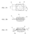
- FIGS. 2A, 2B, and 2C are schematic views illustrating lead pull-out in the lead bending step.
- FIG. 2A and the schematic cross-sectional view of FIG. 2B show the structure after the resin molding step, where the first lead 10 protrudes along the first direction 50.
- FIG. 2C shows the step of bending downward the one end portion 10a and the other end portion 10b.
- the bending stress S and thermal stress due to the difference in linear expansion coefficient may cause the first lead 10 to be easily delaminated from the molded body 30 and pulled out in the direction of the arrow.
- a protruding bent portion is formed on each of the first and second side surfaces 30a, 30b side.
- the stress acts in opposite directions along line A-A, and lead pull-out can be prevented.
- the other end portion 10b may be bent upward.
- the linear expansion coefficient is approximately 1.7 ⁇ 10 -5 /°C for copper and approximately 1.2 ⁇ 10 -5 /°C for iron, but approximately 6.3 ⁇ 10 -5 /°C for epoxy resin.
- the linear expansion coefficient of the resin is several times larger than that of copper. This generates large thermal stress during temperature rise and fall in the soldering step, which may cause delamination.
- one end portion 10b of the first lead 10 and the end portion 20b of the second lead 20 bent downward are further bent to below the lower surface 30c of the molded body 30 to form attachment regions 10c, 20b, respectively.
- This bending can be performed so that the lower surface of these attachment regions 10c, 20b is generally coplanar with or lower than the lower surface 30c of the molded body 30.
- soldering onto a circuit board can be reliably performed by a reflow process and the like.
- the length L10 of the attachment region 10c of the first lead 10 along the first direction 50 and the length L20 of the second lead 20 along the first direction 50 can illustratively be 0.8 mm.
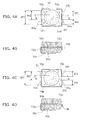
- FIG. 3A is a schematic plan view of a light-emitting device according to a comparative example
- FIG. 3B is a schematic cross-sectional view taken along line B-B.
- the first lead 110 and the second lead 120 have end portions opposed to each other inside a molded body 130.
- the first lead 110 with a light-emitting element 140 bonded thereto is bifurcated inside the molded body 130, and each bifurcated portion protrudes outside from a first side surface 130a,
- the second lead 120 electrically connected to the light-emitting element 140 by wire bonding protrudes outside from a second side surface 130b of the molded body 130.
- the first lead 110 protrudes only from the first side surface 130a.
- this embodiment can prevent pull-out and delamination of the lead from the molded body 30, This facilitates expanding the effective width of the first lead 10 to which the light-emitting element 40 is bonded, and the thermal resistance can be reduced. That is, high output power can be achieved.
- FIG. 4A is a schematic plan view of a first variation of the first embodiment
- FIG. 4B is a schematic cross-sectional view taken along line A-A
- FIG. 4C is a schematic plan view of a second variation
- FIG. 4D is a schematic cross-sectional view taken along line A-A.
- the first lead 10 and the second lead 20 may have anchor holes.
- the molded body 30 penetrates through three round holes 10n of the first lead 10 and a round hole 20d of the second lead 20.
- the round holes 10n, 20d serve as anchor holes. That is, the anchor hole prevents loosening between the lead and the molded body, increases adhesion strength, and increases the contact area. This can avoid delamination between the lead and the molded body and prevent lead pull-out even under stress in the bending step and thermal stress.
- the width of the first lead 10 can be expanded, which further facilitates reducing thermal resistance.
- the round hole or square hole operable as an anchor hole can be smaller than the width W1 of the first lead 10 so as not to interfere with the reduction of thermal resistance.
- part of the small anchor hole may be exposed on the first side surface 30a of the molded body 30.
- the width W1 can be easily made larger than the width W2 even if the width of the small anchor hole is subtracted from the width W1. In this case, it is possible to further increase adhesion strength while maintaining low thermal resistance.
- the anchor hole may be shaped like a square or rectangular hole instead of the round hole. Furthermore, as in the second variation shown in FIG. 4C and 4D , for instance, it is also possible to use a notch 10p provided on each outer edge 10d, 10e of the first lead 10.
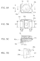
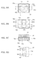
- FIG. 5A is a schematic plan view of a light-emitting device according to a second embodiment
- FIG. 5B is a schematic bottom view thereof
- FIG. 5C is a schematic cross-sectional view taken along line A-A
- FIG. 5D is a schematic side view on the second side surface side.
- the second lead 20 protruding from the second side surface 30b of the molded body 30 is bent downward along the first and second side surfaces 30a, 30b of the molded body 30, and further bent toward the lower surface 30c,
- the end portion 20a of the second lead 20 protrudes from the second side surface 30b with a width narrower than the width W1 of the first lead 10, and expands its width while being bent downward.
- the width of the second lead 20 parallel to the second direction 51 is expanded so as to be generally equal to the width W1 of the first lead 10, thereby forming an attachment region 20e which is further bent toward the lower surface 30c of the molded body 30.
- the attachment region 20c and the attachment region 10c can have a generally symmetrical shape with respect to a line parallel to the second direction 51 so that soldering to a circuit board can be performed with good balance.
- FIG, 6A is a schematic plan view of a light-emitting device according to a third embodiment
- FIG. 6B is a schematic bottom view thereof
- FIG. 6C is a schematic cross-sectional view taken along line A-A.
- the other end portion 10b of the first lead 10 is further bent downward along the second side surface 30b to form an attachment region 10f.
- the width W3 of the attachment region 10f of the first lead 10 can be generally equal to the width W4 of the attachment region 20b of the second lead 20 so that soldering to a circuit board can be performed with good balance.
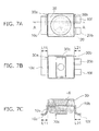
- FIG. 7A is a schematic plan view of a variation of the third embodiment
- FIG. 7B is a schematic bottom view thereof
- FIG. 7C is a schematic side view thereof.
- the first lead 10 may be bent outward from the first side surface 30a of the molded body 30 to form an attachment region 10c with length L11 along the first direction 50. Furthermore, the first lead 10 may be bent outward from the second side surface 30b of the molded body 30 to form an attachment region 20b with length L21 along the first direction 50, and the second lead 20 may be bent outward from the second side surface 30b to form an attachment region 10f with length L21 along the first direction 50, This facilitates attachment to a circuit board and visual inspection.
- the lengths of the attachment regions, L11 and L21 can be made generally equal so that soldering can be performed with good left-right balance.
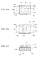
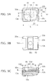
- FIG. 8A is a schematic plan view of a light-emitting device according to a fourth embodiment
- FIG. 8B is a schematic bottom view thereof
- FIG. 8C is a schematic cross-sectional view taken along line A-A
- FIG. 8D is a schematic side view on the first side surface side.
- One end portion 10a protruding from the first side surface 30a of the molded body 30 is bent and further bifurcated.
- the two bifurcated end portions are further bent toward the lower surface 30c to form attachment regions 10h, 10k, This causes little variation in the distribution of heat flow J because the area of the first lead 10 does not change inside the molded body 30.
- the thermal resistance can be left substantially unchanged even if the first lead 10 is bifurcated outside.
- the shape of the attachment regions 10f, 10h, 10k of the first lead 10 and the attachment region 20b of the second lead 20 can be made generally the same and placed at generally symmetrical positions with respect to a line parallel to the first direction 50 and a line parallel to the second direction 51. Then, in soldering to a circuit board by a reflow process, the surface tension of solder is applied with good balance. Imbalance in surface tension or imbalance in the melting condition of solder due to an asymmetrical pattern, if any, may cause mounting failure due to the Manhattan phenomenon (or tombstone phenomenon) in which the surface-mounted device rises up due to increased bonding force of solder on one side. This embodiment prevents such mounting failure and enables reliable bonding to a circuit board.
- the Manhattan phenomenon or tombstone phenomenon
- FIG. 9A is a schematic plan view of a light-emitting device according to a fifth embodiment
- FIG. 9B is a schematic bottom view thereof
- FIG. 9C is a schematic cross-sectional view taken along line A-A.
- the light-emitting element 40 is made of an InGaAIN-based material.
- Yellow phosphor particles made of a silicate material can be dispersed in the sealing resin layer 46 to absorb the light emitted from the light-emitting element 40 and emit wavelength-converted light with a wavelength around yellow.
- white light and an incandescent color can be obtained as mixed light of blue light and yellow light, for instance.
- three or more lights can be mixed using phosphor particles from which visible light in the green to red wavelength range can be emitted as the wavelength-converted light.
- an ESD (electrostatic discharge) protection element 60 such as a Zener diode can be placed in the recess 30d so as to be opposite in polarity to the light-emitting element 40.
- This can increase ESD withstand capability.
- the width SW of the sidewall of the molded body 30 can be narrowed to increase the volume of the recess 30d and facilitate placing the ESD protection element 60 therein while keeping small the planar size of the light-emitting device.
- the width SW of the sidewall is narrowed, the adhesion strength between the molded body 30 and the first lead 10 with the width W1 expanded to reduce thermal resistance is likely to decrease near the region R shown by the dashed line.
- the inner diameter IX of the recess 30d at the upper surface can be as large as 2.84 mm.
- the width SW of the sidewall is illustratively 0.3 mm.
- the width W of the molded body 30 is 2.9 mm, the inner diameter IY of the recess 30d at the upper surface can be as large as 2.54 mm.
- the first lead 10 is bent in the state of protruding from each of the first side surface 30a and the second side surface 30b.
- the stress is relaxed by acting in opposite directions.
- the fifth embodiment can provide a white light-emitting device including an ESD protection element to increase ESD withstand capability.
- the light-emitting device can emit light in the blue to red visible wavelength range.
- the light-emitting device according to the present embodiments which exhibits low thermal resistance and can be attached to a circuit board with good balance while maintaining a small size, can be used as a backlight source of a display device, and a pilot lamp.
Landscapes
- Led Device Packages (AREA)
Applications Claiming Priority (1)
| Application Number | Priority Date | Filing Date | Title |
|---|---|---|---|
| JP2009220339A JP2011071265A (ja) | 2009-09-25 | 2009-09-25 | 発光装置 |
Publications (2)
| Publication Number | Publication Date |
|---|---|
| EP2302709A2 true EP2302709A2 (de) | 2011-03-30 |
| EP2302709A3 EP2302709A3 (de) | 2012-05-30 |
Family
ID=43432102
Family Applications (1)
| Application Number | Title | Priority Date | Filing Date |
|---|---|---|---|
| EP10150219A Withdrawn EP2302709A3 (de) | 2009-09-25 | 2010-01-07 | Lichtemittierende Vorrichtung |
Country Status (5)
| Country | Link |
|---|---|
| US (1) | US8030835B2 (de) |
| EP (1) | EP2302709A3 (de) |
| JP (1) | JP2011071265A (de) |
| CN (1) | CN102034914A (de) |
| TW (1) | TW201112450A (de) |
Families Citing this family (10)
| Publication number | Priority date | Publication date | Assignee | Title |
|---|---|---|---|---|
| JP2013004905A (ja) * | 2011-06-21 | 2013-01-07 | Mitsubishi Chemicals Corp | 半導体発光装置用パッケージ及び半導体発光装置 |
| DE102011056810B4 (de) * | 2011-12-21 | 2022-01-20 | OSRAM Opto Semiconductors Gesellschaft mit beschränkter Haftung | Optoelektronisches Halbleiterbauelement |
| JP2013179271A (ja) * | 2012-01-31 | 2013-09-09 | Rohm Co Ltd | 発光装置および発光装置の製造方法 |
| JP6204088B2 (ja) * | 2013-07-02 | 2017-09-27 | エスアイアイ・セミコンダクタ株式会社 | 半導体装置 |
| US9502623B1 (en) * | 2015-10-02 | 2016-11-22 | Nichia Corporation | Light emitting device |
| US10514131B2 (en) * | 2016-07-06 | 2019-12-24 | Epistar Corporation | Light-emitting apparatus |
| JP6414609B2 (ja) * | 2017-02-28 | 2018-10-31 | 日亜化学工業株式会社 | 発光装置用パッケージ及びそれを備える発光装置、並びにその発光装置を備える照明装置 |
| JP6680274B2 (ja) * | 2017-06-27 | 2020-04-15 | 日亜化学工業株式会社 | 発光装置及び樹脂付リードフレーム |
| KR20190127218A (ko) * | 2018-05-04 | 2019-11-13 | 엘지이노텍 주식회사 | 반도체 소자 패키지 및 이를 포함하는 광조사장치 |
| DE102020107409B4 (de) * | 2020-03-18 | 2023-11-02 | OSRAM Opto Semiconductors Gesellschaft mit beschränkter Haftung | Gehäuse für ein optoelektronisches halbleiterbauelement und optoelektronisches halbleiterbauelement |
Family Cites Families (11)
| Publication number | Priority date | Publication date | Assignee | Title |
|---|---|---|---|---|
| JPS6117759U (ja) * | 1984-07-07 | 1986-02-01 | オムロン株式会社 | 発光器 |
| EP2267797A1 (de) * | 1997-07-29 | 2010-12-29 | OSRAM Opto Semiconductors GmbH | Optoelektronisches Bauelement |
| US6335548B1 (en) * | 1999-03-15 | 2002-01-01 | Gentex Corporation | Semiconductor radiation emitter package |
| JP2002314138A (ja) * | 2001-04-09 | 2002-10-25 | Toshiba Corp | 発光装置 |
| JP3659635B2 (ja) | 2001-04-10 | 2005-06-15 | 株式会社東芝 | 光半導体装置 |
| JP2002368285A (ja) * | 2001-06-11 | 2002-12-20 | Omron Corp | 発光器、発光モジュール及びその製造方法 |
| CN1655368A (zh) * | 2004-02-10 | 2005-08-17 | 翁世杰 | 发光二极管结构及其制作方法 |
| DE102004057804B4 (de) * | 2004-11-30 | 2010-04-08 | Osram Opto Semiconductors Gmbh | Gehäusekörper für einen Halbleiterchip aus gegossener Keramik mit reflektierender Wirkung und Verfahren zu dessen Herstellung |
| JP5091421B2 (ja) * | 2006-04-07 | 2012-12-05 | 株式会社東芝 | 半導体発光装置 |
| JP4922663B2 (ja) * | 2006-05-18 | 2012-04-25 | スタンレー電気株式会社 | 半導体光学装置 |
| JP5326229B2 (ja) * | 2006-09-08 | 2013-10-30 | 日亜化学工業株式会社 | 発光装置 |
-
2009
- 2009-09-25 JP JP2009220339A patent/JP2011071265A/ja active Pending
- 2009-12-01 US US12/628,286 patent/US8030835B2/en active Active
-
2010
- 2010-01-07 EP EP10150219A patent/EP2302709A3/de not_active Withdrawn
- 2010-02-25 TW TW099105525A patent/TW201112450A/zh unknown
- 2010-03-08 CN CN201010129790.5A patent/CN102034914A/zh active Pending
Non-Patent Citations (1)
| Title |
|---|
| None |
Also Published As
| Publication number | Publication date |
|---|---|
| US20110074276A1 (en) | 2011-03-31 |
| EP2302709A3 (de) | 2012-05-30 |
| US8030835B2 (en) | 2011-10-04 |
| CN102034914A (zh) | 2011-04-27 |
| TW201112450A (en) | 2011-04-01 |
| JP2011071265A (ja) | 2011-04-07 |
Similar Documents
| Publication | Publication Date | Title |
|---|---|---|
| US8030835B2 (en) | Light emitting device | |
| KR100809210B1 (ko) | 고출력 led 패키지 및 그 제조방법 | |
| KR101360732B1 (ko) | 발광 다이오드 패키지 | |
| US9112124B2 (en) | Light emitting device | |
| US9646957B2 (en) | LED packaging structure having stacked arrangement of protection element and LED chip | |
| US7964892B2 (en) | Light emitting device | |
| EP2083454A2 (de) | Leuchtdiodenpaket | |
| EP2416388A2 (de) | Lichtemittierende Vorrichtung und Bildanzeigeeinheit | |
| WO2010126592A1 (en) | Led package with increased feature sizes | |
| JP2008060344A (ja) | 半導体発光装置 | |
| US8441022B2 (en) | Semiconductor light-emitting device | |
| JP5458910B2 (ja) | 発光装置 | |
| US9425235B2 (en) | Light emitting device including resin package having differently curved parts | |
| WO2018105448A1 (ja) | 発光装置 | |
| JP6107229B2 (ja) | 発光装置 | |
| EP2315280B1 (de) | Leuchtdiodengehäuse | |
| KR101911866B1 (ko) | 발광 소자 패키지 | |
| US20150053993A1 (en) | Semiconductor light emitting device | |
| JP2007005722A (ja) | 光半導体素子用外囲器およびそれを用いた光半導体装置 | |
| JP2009099823A (ja) | 発光装置 | |
| JP2007280983A (ja) | 発光装置 | |
| JP2008205329A (ja) | 半導体装置 | |
| KR100667532B1 (ko) | 개선된 리드들을 갖는 발광 다이오드 램프 | |
| KR20050113736A (ko) | 발광 다이오드 패키지 | |
| KR20110060425A (ko) | 엘이디 패키지 제조방법 |
Legal Events
| Date | Code | Title | Description |
|---|---|---|---|
| PUAI | Public reference made under article 153(3) epc to a published international application that has entered the european phase |
Free format text: ORIGINAL CODE: 0009012 |
|
| 17P | Request for examination filed |
Effective date: 20100107 |
|
| AK | Designated contracting states |
Kind code of ref document: A2 Designated state(s): AT BE BG CH CY CZ DE DK EE ES FI FR GB GR HR HU IE IS IT LI LT LU LV MC MK MT NL NO PL PT RO SE SI SK SM TR |
|
| AX | Request for extension of the european patent |
Extension state: AL BA RS |
|
| PUAL | Search report despatched |
Free format text: ORIGINAL CODE: 0009013 |
|
| AK | Designated contracting states |
Kind code of ref document: A3 Designated state(s): AT BE BG CH CY CZ DE DK EE ES FI FR GB GR HR HU IE IS IT LI LT LU LV MC MK MT NL NO PL PT RO SE SI SK SM TR |
|
| AX | Request for extension of the european patent |
Extension state: AL BA RS |
|
| RIC1 | Information provided on ipc code assigned before grant |
Ipc: H01L 33/48 20100101AFI20120425BHEP Ipc: H01L 33/62 20100101ALI20120425BHEP |
|
| STAA | Information on the status of an ep patent application or granted ep patent |
Free format text: STATUS: THE APPLICATION IS DEEMED TO BE WITHDRAWN |
|
| 18D | Application deemed to be withdrawn |
Effective date: 20140801 |