EP2302704A2 - Lichtemittierende Vorrichtung und Gehäuse für lichtemittierende Vorrichtung - Google Patents
Lichtemittierende Vorrichtung und Gehäuse für lichtemittierende Vorrichtung Download PDFInfo
- Publication number
- EP2302704A2 EP2302704A2 EP20100166575 EP10166575A EP2302704A2 EP 2302704 A2 EP2302704 A2 EP 2302704A2 EP 20100166575 EP20100166575 EP 20100166575 EP 10166575 A EP10166575 A EP 10166575A EP 2302704 A2 EP2302704 A2 EP 2302704A2
- Authority
- EP
- European Patent Office
- Prior art keywords
- light emitting
- electrode
- emitting device
- layer
- type semiconductor
- Prior art date
- Legal status (The legal status is an assumption and is not a legal conclusion. Google has not performed a legal analysis and makes no representation as to the accuracy of the status listed.)
- Granted
Links
Images



Classifications
-
- H—ELECTRICITY
- H10—SEMICONDUCTOR DEVICES; ELECTRIC SOLID-STATE DEVICES NOT OTHERWISE PROVIDED FOR
- H10H—INORGANIC LIGHT-EMITTING SEMICONDUCTOR DEVICES HAVING POTENTIAL BARRIERS
- H10H20/00—Individual inorganic light-emitting semiconductor devices having potential barriers, e.g. light-emitting diodes [LED]
- H10H20/80—Constructional details
- H10H20/83—Electrodes
- H10H20/831—Electrodes characterised by their shape
-
- H—ELECTRICITY
- H10—SEMICONDUCTOR DEVICES; ELECTRIC SOLID-STATE DEVICES NOT OTHERWISE PROVIDED FOR
- H10H—INORGANIC LIGHT-EMITTING SEMICONDUCTOR DEVICES HAVING POTENTIAL BARRIERS
- H10H20/00—Individual inorganic light-emitting semiconductor devices having potential barriers, e.g. light-emitting diodes [LED]
- H10H20/80—Constructional details
- H10H20/83—Electrodes
- H10H20/832—Electrodes characterised by their material
- H10H20/833—Transparent materials
-
- H—ELECTRICITY
- H10—SEMICONDUCTOR DEVICES; ELECTRIC SOLID-STATE DEVICES NOT OTHERWISE PROVIDED FOR
- H10W—GENERIC PACKAGES, INTERCONNECTIONS, CONNECTORS OR OTHER CONSTRUCTIONAL DETAILS OF DEVICES COVERED BY CLASS H10
- H10W74/00—Encapsulations, e.g. protective coatings
-
- H—ELECTRICITY
- H10—SEMICONDUCTOR DEVICES; ELECTRIC SOLID-STATE DEVICES NOT OTHERWISE PROVIDED FOR
- H10W—GENERIC PACKAGES, INTERCONNECTIONS, CONNECTORS OR OTHER CONSTRUCTIONAL DETAILS OF DEVICES COVERED BY CLASS H10
- H10W90/00—Package configurations
- H10W90/701—Package configurations characterised by the relative positions of pads or connectors relative to package parts
- H10W90/751—Package configurations characterised by the relative positions of pads or connectors relative to package parts of bond wires
- H10W90/756—Package configurations characterised by the relative positions of pads or connectors relative to package parts of bond wires between a chip and a stacked lead frame, conducting package substrate or heat sink
Definitions
- a light emitting device and a light emitting device package are disclosed herein.
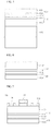
- Fig. 1 is a sectional view of a light emitting device according to an embodiment
- Fig. 2 is a plan view and a partially enlarged view of a light emitting device according to an embodiment
- Fig. 3 is a chart illustrating light extraction efficiency of a light emitting device according to an embodiment
- Figs. 4 to 7 are sectional views illustrating a process of manufacturing a light emitting device according to an embodiment
- Fig. 8 is a plan view and a partially enlarged view of a light emitting device according to another embodiment.
- Fig. 9 is a sectional view of a light emitting device package according to embodiments.
- a layer (or film) is referred to as being 'on' another layer or substrate, it may be directly on the another layer or substrate, or intervening layers may also be present. Further, it should be understood that when a layer is referred to as being 'under' another layer, it can be directly under the another layer, and one or more intervening layers may also be present. In addition, it should also be understood that when a layer is referred to as being 'between' two layers, it may be the only layer between the two layers, or one or more intervening layers may also be present.
- Fig. 1 is a sectional view of a light emitting device according to an embodiment
- Fig. 2 is a plan view and a partially enlarged view of a light emitting device according to an embodiment.
- a light emitting device 100 may include a light emitting structure 110, a first electrode 130, and a pad electrode 140.
- the light emitting structure 110 may include a first conductive type semiconductor layer 112, an active layer 114, and a second conductive type semiconductor layer 116.
- the first electrode 130 may include patterns H formed on the light emitting structure.
- the pad electrode 140 may be formed on the first electrode 130.
- the first electrode 130 may include a first ohmic layer 132, and the first ohmic layer 132 may include a transparent ohmic layer; however, embodiments are not limited thereto.
- the first ohmic layer may include the transparent ohmic layer and may have a thickness of about 20 nm or less; however, embodiments are not limited thereto.
- the first ohmic layer 132 may be formed, for example, of at least one of chromium (Cr), platinum (Pt), nickel (Ni), aurum (Au), and titanium (Ti).
- the first electrode 130 may have a structure in which an electrode metal may be deposited on an entire region of the light emitting structure 110 to form periodic or aperiodic patterns using, for example, a dry or wet etch process. According to one embodiment, the first electrode 130 may serve as a light extraction structure at the same time due to the periodic or aperiodic patterns within a planar metal layer.
- the first electrode 130 may be uniformly distributed on an upper end of the entire region of the light emitting structure 110, light may be uniformly emitted over a light emitting layer (the active layer). As a result, reliability of a high power LED may be improved.
- a n-type electrode may serve as only a reflective mirror.
- the first electrode 130 may additionally perform a function in which a portion of light is extracted to the outside through the patterns H of a boundary of a metal/dielectric layer (an example of a material for filling the patterns).
- the patterns H formed on the boundary of the metal/dielectric may have good light extraction properties when compared to patterns formed on a boundary of a general dielectric. This is because the light extraction efficiency may be in proportion to a reflective index difference between two materials with a boundary therebetween.
- Fig. 3 is a chart illustrating light extraction efficiency of a light emitting device according to an embodiment.
- Fig. 3 illustrates a change of light extraction efficiency according to a reflective index and a pattern height h of a dielectric when patterns of about 400 nm are formed on a boundary of a metal/dielectric.
- the dotted line represents light extraction efficiency when patterns are not formed.
- the first electrode since the first electrode may include predetermined patterns within the planar metal layer, current diffusion may be easy, and simultaneously, the light extraction efficiency may be improved. Also, according to one embodiment, since the first electrode may include a thin transparent metal in a remaining region except in a location of a wire bonding pad, operation voltage characteristics may be satisfied, and also, light quantity may increase.
- a method of manufacturing a light emitting device will be described with reference to Figs. 4 to 7 .
- a light emitting structure 110 which may include a first conductive type semiconductor layer 112, an active layer 114, and a second conductive type semiconductor layer 116 may be formed.
- a first substrate 105 may be prepared.
- the first substrate 105 may include, for example, a sapphire (Al 2 O 3 ) substrate and a SiC substrate; however, embodiments are not limited thereto.
- a wet cleaning process may be performed on the first substrate 105 to remove impurities from a surface of the first substrate 105.
- the light emitting structure 110 including the first conductive type semiconductor layer 112, the active layer 114, and the second conductive type semiconductor layer 116 may be formed on the first substrate 105.
- an N-type GaN layer may be formed using, for example, a chemical vapor deposition (CVD) process, molecular beam epitaxy (MBE) process, sputtering process, or hydrid vapour phase epitaxy process.
- silane gas (SiH 4 ) containing n-type impurities such as trimethyl gallium (TMGa) gas, ammonia (NH 3 ) gas, nitrogen (N 2 ) gas, and silicon (Si), may be injected into a chamber to form the first conductive type semiconductor layer 112.
- TMGa trimethyl gallium
- NH 3 ammonia
- N 2 nitrogen
- Si silicon
- an undoped semiconductor layer (not shown) may be formed on the first substrate 105.
- the first conductive type semiconductor layer 112 may be formed on the undoped semiconductor layer to reduce a crystal lattice difference between the substrate and the light emitting structure.
- the active layer 114 may serve as a layer in which electrons injected through the first conductive type semiconductor layer 112 recombine with electron holes injected through a second conductive type semiconductor layer 116 to emit light having an energy determined by a proper energy band of an active layer (a light emitting layer) material.
- the active layer 114 may have at least one of, for example, a single quantum well structure, a multi-quantum well (MQW) structure, a quantum-wire structure, or a quantum dot structure.
- MQW multi-quantum well
- trimethyl gallium (TMGa) gas, ammonia (NH3) gas, nitrogen (N2) gas, and trimethyl indium (TMIn) gas may be injected to form the multi-quantum well (MQW) structure having an InGaN/GaN structure or an InGaN/InGaN structure; however, embodiments are not limited thereto.
- bis(ethylcyclopentadienyl) magnesium [EtC p2 Mg:Mg(C 2 H 5 C 5 H 4 ) 2 ] containing p-type impurities, such as trimethyl gallium (TMGa) gas, ammonia (NH 3 ) gas, nitrogen (N 2 ) gas, and magnesium (Mg) gas may be injected into the chamber to form a p-type GaN layer; however, embodiments are not limited thereto.
- TMGa trimethyl gallium
- NH 3 ammonia
- N 2 nitrogen
- Mg magnesium
- a second electrode 120 may be formed on the second conductive type semiconductor layer 116.
- the second electrode 120 may include a second ohmic layer 122, a second reflective layer 125, a second coupling layer 128, and a second or conductive substrate 124.
- the second electrode 120 may include, for example, at least one of titanium (Ti), chrome (Cr), nickel (Ni), aluminium (Al), platinum (Pt), gold (Au), tungsten (W) or copper (Cu), a Cu alloy, Si, molybdenum (mo), SiGe, Ge, Ga 2 O 3 , or GaN.
- the second electrode layer 120 may include the second ohmic layer 122.
- a single metal or a metal alloy and a metal oxide may be multi-stacked to improve the efficiency of electron hole injection.
- the second ohmic layer 122 may be formed of at least one of ITO, ZnO, IZO(IN-ZnO), GZO(Ga-ZnO), AZO(Al-ZnO), AGZO(Al-Ga ZnO), IGZO(In-Ga ZnO), IrOx, RuOx, RuOx/ITO, Ni/IrOx/Au, and Ni/IrOx/Au/ITO; however, embodiments are not limited thereto.
- the second electrode layer 120 when the second electrode layer 120 includes the second reflective layer, the second electrode layer 120 may include a metal layer containing Al, Ag, or an alloy containing Al or Ag. Light generated in the active layer may be effectively reflected by Al or Ag to significantly improve light extraction efficiency of the light emitting device. Additionally, when the second electrode layer 120 includes the second coupling layer, the second reflective layer may serve as the second coupling layer, or the second coupling layer may be formed using Ni or Au.
- the second electrode layer 120 may include the second substrate 124. If the first conductive type semiconductor layer 112 has a sufficiently thick thickness, for example, a thickness of about 50 ⁇ m or more, a process of forming the second substrate 124 may be omitted.
- the second substrate 124 may be formed of a metal having good conductive properties, a metal alloy, or a conductive semiconductor material to efficiently inject the electron holes.
- the second substrate 124 may be formed of one or more of copper (Cu), a Cu alloy, Si, molybdenum (Mo), SiGe, Ge, Ga 2 O 3 , or GaN.
- the second substrate 124 may be formed using, for example, an electrochemical metal deposition method or a bonding method using eutectic metals.
- the first substrate 105 may be removed to expose the first conductive type semiconductor layer 112.
- the first substrate 105 may be separated, for example, using a high power laser, or removed, for example, using a chemical etching process. Also, the first substrate 105 may be removed, for example, by being physically grinded.
- a first electrode 130 which may include patterns may be formed on the light emitting structure 110.
- a surface roughness (not shown) or a periodic surface structure (not shown) may be formed before the first electrode 130 is formed on the light emitting structure 110.
- a first electrode material (not shown) may be formed on the light emitting structure 110, and then, the first electrode material may be patterned using, for example, a wet or dry etch process to form the patterns H.
- the first electrode 130 which may define a region of a pad electrode 140 to be formed later, may have a wider area to correspond to the pad electrode 140; however, embodiments are not limited thereto.
- the process of forming the first electrode 130 may include forming a first ohmic layer 132 on the light emitting structure 110 and forming a first reflective layer 134 on the first ohmic layer 132.
- Fig. 8 is a plan view and a partially enlarged view of a light emitting device according to another embodiment.
- a first electrode 130 may include a first ohmic layer 132, and the first ohmic layer 132 may include a transparent ohmic layer.
- the first ohmic layer 132 may have a thickness of about 20 nm or less. Also, the first ohmic layer 132 may be formed of one or more of Cr, Pt, Ni, Au, and Ti; however, embodiments are not limited thereto.
- the respective patterns H of the first electrode 130 may include, for example, a triangular lattice, a square lattice, or an Archimedean lattice using the same, or a quasicrystal. Also, the patterns H may include irregular random patterns in addition to the periodic patterns. Further, in this embodiment, the patterns H of the first electrode 130 may have a hole shape in which the patterns H are connected to each other to improve current diffusion. The patterns H applied in this embodiment may have a period ranging from about 100 nm to about 5,000 nm, and the first electrode 130 may occupy an area ranging from about 5% to about 95% of a total LED chip area.
- the patterns H may be filled with at least one or more of air, epoxy, or other dielectrics.
- the dielectric may have a reflective index of greater than approximately 1 and less than approximately 3.
- a photoresist or an insulating material may be formed in the pattern region and an additional material may be formed on the first electrode 130 to selectively remove the photoresist or the insulating material.
- a pad electrode 140 may be formed on the first electrode 130.
- the pad electrode 140 may include a third coupling layer 146 for metal interface bonding and a bonding layer 148 for wire bonding to improve the current diffusion; however, embodiments are not limited thereto.
- the bonding layer and the coupling layer may be omitted in a remaining region except for a region of the pad electrode 140, as shown in Fig. 2 .
- the first electrode 130 may include the first ohmic layer 132 and the first reflective layer 133, as shown in Fig. 2 .
- the pad electrode 140 When the pad electrode 140 includes the third coupling layer 146, the third coupling layer 146 may be formed using Ni or Au. Also, the pad electrode 140 may include the bonding layer 148 due to Au.
- the reflective layer may be omitted in the first electrode 130.
- the first ohmic layer 132 when a metal of the first ohmic layer 132 is formed in the remaining region except the region of the pad electrode 140, the first ohmic layer 132 may have a thickness of about 20 nm or less to server as a transparent metal layer.
- the pad electrode 140 may further include a third reflective layer 144 that reflects light.
- the third reflective layer 144 may include a metal layer containing Al, Ag, or an alloy containing Al or Ag.
- the first electrode may include predetermined patterns within the planar metal layer, current diffusion may be easy, and simultaneously, the light extraction efficiency may be improved. Also, since the first electrode may include a thin transparent metal in a remaining region except for a location of a wire bonding pad, operation voltage characteristics may be satisfied, and also, light quantity may increase.
- Fig. 9 is a sectional view of a light emitting device package according to embodiments.
- a light emitting device package according to embodiments may include a body 200, a third electrode layer 210 and a fourth electrode layer 220 formed in the body 200, a light emitting device 100 formed in the body 200 and electrically connected via a wire 300 to the third electrode layer 210 and the fourth electrode layer 220, and a molding member 400 that encapsulates the light emitting device 100.
- the body 200 may be formed, for example, of a silicon material, a synthetic resin material, or a metal material.
- An inclined surface may be formed around the light emitting device 100.
- the third electrode layer 210 and the fourth electrode layer 220 may be electrically separated from each other and supply a power to the light emitting device 100. Also, the third electrode layer 210 and the fourth electrode layer 220 may reflect light generated in the light emitting device 100 to improve light efficiency. In addition, the third electrode layer 210 and the fourth electrode layer 220 may release heat generated in the light emitting device 100 to the outside.
- a vertical type light emitting device as illustrated in Fig. 1 may be applicable as the light emitting device 100 according to this embodiment; however, embodiments are not limited thereto.
- the light emitting device 100 may be formed on the package body 200 or on the third electrode layer 210 or the fourth electrode layer 220.
- the light emitting device 100 may be electrically connected to the third electrode layer 210 and/or the fourth electrode layer 220 by, for example, a wire.
- a wire since a vertical type light emitting device 100 is used as an example, one wire 300 may be used.
- the light emitting device 100 is a horizontal type light emitting device, two wires may be used.
- the light emitting device 100 includes a flip chip type light emitting device, the wire may not be necessary or used.
- the molding member 400 may encapsulate the light emitting device 100 and protect the light emitting device 100. Also, a phosphor may be contained in the molding member 400 to vary a wavelength of light emitted from the light emitting device 100.
- a light emitting device may be varied in light quantity or electrical characteristics, that is, an operation voltage according to an area or a configuration of an electrode, and as an area of the electrode increases, operation voltage characteristics may be improved, but the light quantity reduced.
- Embodiments disclosed herein provide a light emitting device that may include an electrode to satisfy operation voltage characteristics and improve light quantity, a method of manufacturing the light emitting device, and a light emitting device package.
- a light emitting device may include a light emitting structure including a first conductive type semiconductor layer, an active layer, and a second conductive type semiconductor layer; a first electrode on the light emitting structure, the first electrode comprising a pattern; and a pad electrode on the first electrode.
- a light emitting device package may include a light emitting device including a light emitting structure, a first electrode on the light emitting structure, the first electrode including a pattern, and a pad electrode on the first electrode; and a package body, wherein the light emitting device is formed in the package body.
- any reference in this specification to "one embodiment,” “an embodiment,” “example embodiment,” etc. means that a particular feature, structure, or characteristic described in connection with the embodiment is included in at least one embodiment of the invention.
- the appearances of such phrases in various places in the specification are not necessarily all referring to the same embodiment.
Landscapes
- Led Devices (AREA)
- Led Device Packages (AREA)
Applications Claiming Priority (1)
| Application Number | Priority Date | Filing Date | Title |
|---|---|---|---|
| KR1020090089902A KR101081166B1 (ko) | 2009-09-23 | 2009-09-23 | 발광소자, 발광소자의 제조방법 및 발광소자 패키지 |
Publications (3)
| Publication Number | Publication Date |
|---|---|
| EP2302704A2 true EP2302704A2 (de) | 2011-03-30 |
| EP2302704A3 EP2302704A3 (de) | 2014-11-26 |
| EP2302704B1 EP2302704B1 (de) | 2019-11-20 |
Family
ID=42646461
Family Applications (1)
| Application Number | Title | Priority Date | Filing Date |
|---|---|---|---|
| EP10166575.0A Active EP2302704B1 (de) | 2009-09-23 | 2010-06-18 | Lichtemittierende Vorrichtung und Gehäuse für lichtemittierende Vorrichtung |
Country Status (4)
| Country | Link |
|---|---|
| US (1) | US9130123B2 (de) |
| EP (1) | EP2302704B1 (de) |
| KR (1) | KR101081166B1 (de) |
| CN (1) | CN102024894B (de) |
Families Citing this family (2)
| Publication number | Priority date | Publication date | Assignee | Title |
|---|---|---|---|---|
| CN102810613B (zh) * | 2011-05-30 | 2016-04-13 | 比亚迪股份有限公司 | 电流扩散电极、半导体发光器件及其制备方法 |
| CN107611236B (zh) * | 2017-10-10 | 2020-05-19 | 佛山市国星半导体技术有限公司 | 一种led芯片及其制作方法 |
Family Cites Families (57)
| Publication number | Priority date | Publication date | Assignee | Title |
|---|---|---|---|---|
| JP3469484B2 (ja) | 1998-12-24 | 2003-11-25 | 株式会社東芝 | 半導体発光素子およびその製造方法 |
| JP2001156329A (ja) | 1999-11-24 | 2001-06-08 | Hamamatsu Photonics Kk | 半導体発光素子 |
| US6420732B1 (en) | 2000-06-26 | 2002-07-16 | Luxnet Corporation | Light emitting diode of improved current blocking and light extraction structure |
| JP2002170989A (ja) * | 2000-12-04 | 2002-06-14 | Sharp Corp | 窒化物系化合物半導体発光素子 |
| EP1406314B1 (de) | 2001-07-12 | 2015-08-19 | Nichia Corporation | Halbleiterbauelement |
| TW508845B (en) | 2001-11-05 | 2002-11-01 | Epitech Technology Corp | Light emitting diode structure |
| JP2004055646A (ja) * | 2002-07-17 | 2004-02-19 | Sumitomo Electric Ind Ltd | 発光ダイオード素子のp側電極構造 |
| KR100543696B1 (ko) | 2002-09-09 | 2006-01-20 | 삼성전기주식회사 | 고효율 발광 다이오드 |
| US7105861B2 (en) * | 2003-04-15 | 2006-09-12 | Luminus Devices, Inc. | Electronic device contact structures |
| JP4572604B2 (ja) * | 2003-06-30 | 2010-11-04 | 日亜化学工業株式会社 | 半導体発光素子及びそれを用いた発光装置 |
| KR20050008035A (ko) | 2003-07-14 | 2005-01-21 | (주)아트세미텍 | 조명용 고출력 다전극 발광 다이오드 칩 |
| KR20050008259A (ko) | 2003-07-15 | 2005-01-21 | (주)아트세미텍 | 고휘도 고절대정격 발광 다이오드 칩 |
| JP3841092B2 (ja) | 2003-08-26 | 2006-11-01 | 住友電気工業株式会社 | 発光装置 |
| WO2005022654A2 (en) | 2003-08-28 | 2005-03-10 | Matsushita Electric Industrial Co.,Ltd. | Semiconductor light emitting device, light emitting module, lighting apparatus, display element and manufacturing method of semiconductor light emitting device |
| KR100648444B1 (ko) | 2003-11-18 | 2006-11-24 | 나이넥스 주식회사 | 고휘도 발광소자 및 그 제작 방법 |
| US20050173714A1 (en) | 2004-02-06 | 2005-08-11 | Ho-Shang Lee | Lighting system with high and improved extraction efficiency |
| US7250635B2 (en) | 2004-02-06 | 2007-07-31 | Dicon Fiberoptics, Inc. | Light emitting system with high extraction efficency |
| TWI244220B (en) * | 2004-02-20 | 2005-11-21 | Epistar Corp | Organic binding light-emitting device with vertical structure |
| JP4805831B2 (ja) | 2004-03-18 | 2011-11-02 | パナソニック株式会社 | 半導体発光装置、照明モジュール、照明装置、表面実装部品、および表示装置 |
| CN1993835A (zh) | 2004-06-14 | 2007-07-04 | 三菱电线工业株式会社 | 氮化物半导体发光器件 |
| US7557380B2 (en) | 2004-07-27 | 2009-07-07 | Cree, Inc. | Light emitting devices having a reflective bond pad and methods of fabricating light emitting devices having reflective bond pads |
| US8115212B2 (en) * | 2004-07-29 | 2012-02-14 | Showa Denko K.K. | Positive electrode for semiconductor light-emitting device |
| CN100590898C (zh) | 2004-07-29 | 2010-02-17 | 昭和电工株式会社 | 用于半导体发光器件的正电极 |
| CN100342558C (zh) | 2004-08-11 | 2007-10-10 | 深圳市瑞丰光电子有限公司 | 陶瓷封装发光二极管的封装方法 |
| US20060226429A1 (en) | 2005-04-08 | 2006-10-12 | Sigalas Mihail M | Method and apparatus for directional organic light emitting diodes |
| KR100878433B1 (ko) | 2005-05-18 | 2009-01-13 | 삼성전기주식회사 | 발광소자의 오믹컨택층 제조방법 및 이를 이용한발광소자의 제조방법 |
| JP4947954B2 (ja) | 2005-10-31 | 2012-06-06 | スタンレー電気株式会社 | 発光素子 |
| JP4986445B2 (ja) | 2005-12-13 | 2012-07-25 | 昭和電工株式会社 | 窒化ガリウム系化合物半導体発光素子 |
| KR100819883B1 (ko) * | 2006-02-17 | 2008-04-07 | 삼성전자주식회사 | 발광소자 패키지 및 그 제조방법 |
| JP2007287851A (ja) | 2006-04-14 | 2007-11-01 | Toyoda Gosei Co Ltd | 光通信に用いる発光素子およびこれを用いた通信装置 |
| KR100736623B1 (ko) | 2006-05-08 | 2007-07-09 | 엘지전자 주식회사 | 수직형 발광 소자 및 그 제조방법 |
| KR100786091B1 (ko) | 2006-06-08 | 2007-12-18 | 엘지전자 주식회사 | 수평형 발광 소자 및 그 제조방법 |
| JP2008047871A (ja) | 2006-07-18 | 2008-02-28 | Mitsubishi Electric Corp | 半導体発光ダイオード |
| KR100826375B1 (ko) | 2006-08-24 | 2008-05-02 | 삼성전기주식회사 | 질화물 반도체 발광소자 및 제조 방법 |
| JP4922404B2 (ja) | 2006-09-25 | 2012-04-25 | ソウル オプト デバイス カンパニー リミテッド | 電流分散のための電極延長部を有する発光ダイオード |
| JP4835377B2 (ja) | 2006-10-20 | 2011-12-14 | 日立電線株式会社 | 半導体発光素子 |
| US7692203B2 (en) | 2006-10-20 | 2010-04-06 | Hitachi Cable, Ltd. | Semiconductor light emitting device |
| CN101536201A (zh) * | 2006-11-17 | 2009-09-16 | 3M创新有限公司 | 具有光学提取器的平面化发光二极管 |
| KR100847847B1 (ko) | 2007-01-22 | 2008-07-23 | 삼성전기주식회사 | 백색 발광소자 및 그 제조방법 |
| CN102779918B (zh) | 2007-02-01 | 2015-09-02 | 日亚化学工业株式会社 | 半导体发光元件 |
| JP2008283037A (ja) | 2007-05-11 | 2008-11-20 | Hitachi Cable Ltd | 発光素子 |
| KR100850667B1 (ko) | 2007-05-22 | 2008-08-07 | 서울옵토디바이스주식회사 | 발광 다이오드 및 그 제조방법 |
| KR101341374B1 (ko) | 2007-07-30 | 2013-12-16 | 삼성전자주식회사 | 광자결정 발광소자 및 그 제조방법 |
| JP4829190B2 (ja) * | 2007-08-22 | 2011-12-07 | 株式会社東芝 | 発光素子 |
| KR20090053307A (ko) | 2007-11-23 | 2009-05-27 | 한국광기술원 | 질화물계 발광소자 및 그의 제조방법 |
| KR101428053B1 (ko) | 2007-12-13 | 2014-08-08 | 엘지이노텍 주식회사 | 반도체 발광소자 및 그 제조방법 |
| KR101221281B1 (ko) | 2008-03-13 | 2013-01-11 | 쇼와 덴코 가부시키가이샤 | 반도체 발광 소자 및 그 제조 방법 |
| JP5651288B2 (ja) | 2008-03-25 | 2015-01-07 | 株式会社東芝 | 半導体発光素子及びその製造方法 |
| KR101092079B1 (ko) | 2008-04-24 | 2011-12-12 | 엘지이노텍 주식회사 | 반도체 발광소자 및 그 제조방법 |
| US8278679B2 (en) | 2008-04-29 | 2012-10-02 | Tsmc Solid State Lighting Ltd. | LED device with embedded top electrode |
| KR100941616B1 (ko) | 2008-05-15 | 2010-02-11 | 주식회사 에피밸리 | 반도체 발광소자 |
| KR20100030472A (ko) | 2008-09-10 | 2010-03-18 | 삼성전자주식회사 | 발광 소자 및 발광 장치의 제조 방법, 상기 방법을 이용하여 제조한 발광 소자 및 발광 장치 |
| TWI473292B (zh) | 2008-12-15 | 2015-02-11 | Lextar Electronics Corp | 發光二極體晶片 |
| JP2011054598A (ja) | 2009-08-31 | 2011-03-17 | Toshiba Corp | 半導体発光素子およびその製造方法 |
| KR101123012B1 (ko) | 2009-10-23 | 2012-03-19 | 삼성엘이디 주식회사 | 반도체 발광소자 |
| JP5150684B2 (ja) | 2010-07-13 | 2013-02-20 | 株式会社東芝 | 半導体発光素子および半導体発光素子の製造方法 |
| JP5608589B2 (ja) | 2011-03-10 | 2014-10-15 | スタンレー電気株式会社 | 半導体発光素子および半導体発光素子の製造方法 |
-
2009
- 2009-09-23 KR KR1020090089902A patent/KR101081166B1/ko not_active Expired - Fee Related
-
2010
- 2010-06-04 US US12/793,781 patent/US9130123B2/en not_active Expired - Fee Related
- 2010-06-12 CN CN201010205332.5A patent/CN102024894B/zh active Active
- 2010-06-18 EP EP10166575.0A patent/EP2302704B1/de active Active
Non-Patent Citations (1)
| Title |
|---|
| None |
Also Published As
| Publication number | Publication date |
|---|---|
| US9130123B2 (en) | 2015-09-08 |
| EP2302704A3 (de) | 2014-11-26 |
| CN102024894A (zh) | 2011-04-20 |
| US20110068355A1 (en) | 2011-03-24 |
| CN102024894B (zh) | 2017-04-12 |
| KR101081166B1 (ko) | 2011-11-07 |
| KR20110032425A (ko) | 2011-03-30 |
| EP2302704B1 (de) | 2019-11-20 |
Similar Documents
| Publication | Publication Date | Title |
|---|---|---|
| KR101007077B1 (ko) | 발광소자, 발광소자 패키지 및 그 제조방법 | |
| KR101064053B1 (ko) | 발광소자 및 그 제조방법 | |
| US8853731B2 (en) | Semiconductor light emitting device including bonding layer and semiconductor light emitting device package | |
| KR100999779B1 (ko) | 발광소자, 발광소자의 제조방법 및 발광소자 패키지 | |
| KR100974787B1 (ko) | 발광 소자, 발광 소자 제조방법 및 발광 소자 패키지 | |
| KR100986407B1 (ko) | 발광소자 및 그 제조방법 | |
| KR101007139B1 (ko) | 발광소자 및 그 제조방법 | |
| US8853719B2 (en) | Semiconductor light-emitting device and light-emitting device package having the same | |
| EP2221873A1 (de) | Lichtemittierende Vorrichtung | |
| KR101646255B1 (ko) | 발광 소자, 발광 소자 패키지 및 발광 소자 제조방법 | |
| KR100993094B1 (ko) | 발광소자 및 발광소자 패키지 | |
| US8362514B2 (en) | Vertical semiconductor light emitting device including a capacitor | |
| CN101877381B (zh) | 发光器件和发光器件封装 | |
| KR101134802B1 (ko) | 발광소자, 발광소자의 제조방법 및 발광소자 패키지 | |
| KR101103892B1 (ko) | 발광소자 및 발광소자 패키지 | |
| KR100999756B1 (ko) | 발광소자 및 그 제조방법 | |
| KR20120005756A (ko) | 발광소자 | |
| KR102164087B1 (ko) | 발광소자 및 이를 구비한 발광소자 패키지 | |
| EP2302704B1 (de) | Lichtemittierende Vorrichtung und Gehäuse für lichtemittierende Vorrichtung | |
| KR101007145B1 (ko) | 발광소자 칩, 발광소자 패키지 및 발광소자 칩의 제조방법 | |
| KR101081061B1 (ko) | 발광소자, 발광소자의 제조방법 및 발광소자 패키지 | |
| KR101172136B1 (ko) | 발광소자, 발광소자의 제조방법 및 발광소자 패키지 | |
| KR101189429B1 (ko) | 발광소자, 발광소자 제조방법 및 발광소자 패키지 | |
| KR20110101816A (ko) | 발광소자, 발광소자의 제조방법 및 발광소자 패키지 | |
| KR20110093479A (ko) | 발광소자, 발광소자의 제조방법 및 발광소자 패키지 |
Legal Events
| Date | Code | Title | Description |
|---|---|---|---|
| PUAI | Public reference made under article 153(3) epc to a published international application that has entered the european phase |
Free format text: ORIGINAL CODE: 0009012 |
|
| 17P | Request for examination filed |
Effective date: 20100618 |
|
| AK | Designated contracting states |
Kind code of ref document: A2 Designated state(s): AL AT BE BG CH CY CZ DE DK EE ES FI FR GB GR HR HU IE IS IT LI LT LU LV MC MK MT NL NO PL PT RO SE SI SK SM TR |
|
| AX | Request for extension of the european patent |
Extension state: BA ME RS |
|
| RAP1 | Party data changed (applicant data changed or rights of an application transferred) |
Owner name: LG INNOTEK CO., LTD. |
|
| PUAL | Search report despatched |
Free format text: ORIGINAL CODE: 0009013 |
|
| AK | Designated contracting states |
Kind code of ref document: A3 Designated state(s): AL AT BE BG CH CY CZ DE DK EE ES FI FR GB GR HR HU IE IS IT LI LT LU LV MC MK MT NL NO PL PT RO SE SI SK SM TR |
|
| AX | Request for extension of the european patent |
Extension state: BA ME RS |
|
| RIC1 | Information provided on ipc code assigned before grant |
Ipc: H01L 33/00 20100101AFI20141021BHEP |
|
| RBV | Designated contracting states (corrected) |
Designated state(s): AL AT BE BG CH CY CZ DE DK EE ES FI FR GB GR HR HU IE IS IT LI LT LU LV MC MK MT NL NO PL PT RO SE SI SK SM TR |
|
| RAP1 | Party data changed (applicant data changed or rights of an application transferred) |
Owner name: LG INNOTEK CO., LTD. |
|
| STAA | Information on the status of an ep patent application or granted ep patent |
Free format text: STATUS: EXAMINATION IS IN PROGRESS |
|
| 17Q | First examination report despatched |
Effective date: 20180123 |
|
| REG | Reference to a national code |
Ref country code: DE Ref legal event code: R079 Ref document number: 602010062009 Country of ref document: DE Free format text: PREVIOUS MAIN CLASS: H01L0033000000 Ipc: H01L0033380000 |
|
| RIC1 | Information provided on ipc code assigned before grant |
Ipc: H01L 33/38 20100101AFI20180620BHEP Ipc: H01L 33/42 20100101ALI20180620BHEP |
|
| GRAP | Despatch of communication of intention to grant a patent |
Free format text: ORIGINAL CODE: EPIDOSNIGR1 |
|
| STAA | Information on the status of an ep patent application or granted ep patent |
Free format text: STATUS: GRANT OF PATENT IS INTENDED |
|
| INTG | Intention to grant announced |
Effective date: 20190606 |
|
| GRAS | Grant fee paid |
Free format text: ORIGINAL CODE: EPIDOSNIGR3 |
|
| GRAA | (expected) grant |
Free format text: ORIGINAL CODE: 0009210 |
|
| STAA | Information on the status of an ep patent application or granted ep patent |
Free format text: STATUS: THE PATENT HAS BEEN GRANTED |
|
| AK | Designated contracting states |
Kind code of ref document: B1 Designated state(s): AL AT BE BG CH CY CZ DE DK EE ES FI FR GB GR HR HU IE IS IT LI LT LU LV MC MK MT NL NO PL PT RO SE SI SK SM TR |
|
| REG | Reference to a national code |
Ref country code: GB Ref legal event code: FG4D |
|
| REG | Reference to a national code |
Ref country code: CH Ref legal event code: EP |
|
| REG | Reference to a national code |
Ref country code: IE Ref legal event code: FG4D |
|
| REG | Reference to a national code |
Ref country code: DE Ref legal event code: R096 Ref document number: 602010062009 Country of ref document: DE |
|
| REG | Reference to a national code |
Ref country code: AT Ref legal event code: REF Ref document number: 1205180 Country of ref document: AT Kind code of ref document: T Effective date: 20191215 |
|
| REG | Reference to a national code |
Ref country code: NL Ref legal event code: MP Effective date: 20191120 |
|
| REG | Reference to a national code |
Ref country code: LT Ref legal event code: MG4D |
|
| PG25 | Lapsed in a contracting state [announced via postgrant information from national office to epo] |
Ref country code: ES Free format text: LAPSE BECAUSE OF FAILURE TO SUBMIT A TRANSLATION OF THE DESCRIPTION OR TO PAY THE FEE WITHIN THE PRESCRIBED TIME-LIMIT Effective date: 20191120 Ref country code: NL Free format text: LAPSE BECAUSE OF FAILURE TO SUBMIT A TRANSLATION OF THE DESCRIPTION OR TO PAY THE FEE WITHIN THE PRESCRIBED TIME-LIMIT Effective date: 20191120 Ref country code: NO Free format text: LAPSE BECAUSE OF FAILURE TO SUBMIT A TRANSLATION OF THE DESCRIPTION OR TO PAY THE FEE WITHIN THE PRESCRIBED TIME-LIMIT Effective date: 20200220 Ref country code: GR Free format text: LAPSE BECAUSE OF FAILURE TO SUBMIT A TRANSLATION OF THE DESCRIPTION OR TO PAY THE FEE WITHIN THE PRESCRIBED TIME-LIMIT Effective date: 20200221 Ref country code: FI Free format text: LAPSE BECAUSE OF FAILURE TO SUBMIT A TRANSLATION OF THE DESCRIPTION OR TO PAY THE FEE WITHIN THE PRESCRIBED TIME-LIMIT Effective date: 20191120 Ref country code: BG Free format text: LAPSE BECAUSE OF FAILURE TO SUBMIT A TRANSLATION OF THE DESCRIPTION OR TO PAY THE FEE WITHIN THE PRESCRIBED TIME-LIMIT Effective date: 20200220 Ref country code: LT Free format text: LAPSE BECAUSE OF FAILURE TO SUBMIT A TRANSLATION OF THE DESCRIPTION OR TO PAY THE FEE WITHIN THE PRESCRIBED TIME-LIMIT Effective date: 20191120 Ref country code: LV Free format text: LAPSE BECAUSE OF FAILURE TO SUBMIT A TRANSLATION OF THE DESCRIPTION OR TO PAY THE FEE WITHIN THE PRESCRIBED TIME-LIMIT Effective date: 20191120 Ref country code: SE Free format text: LAPSE BECAUSE OF FAILURE TO SUBMIT A TRANSLATION OF THE DESCRIPTION OR TO PAY THE FEE WITHIN THE PRESCRIBED TIME-LIMIT Effective date: 20191120 |
|
| PG25 | Lapsed in a contracting state [announced via postgrant information from national office to epo] |
Ref country code: HR Free format text: LAPSE BECAUSE OF FAILURE TO SUBMIT A TRANSLATION OF THE DESCRIPTION OR TO PAY THE FEE WITHIN THE PRESCRIBED TIME-LIMIT Effective date: 20191120 Ref country code: IS Free format text: LAPSE BECAUSE OF FAILURE TO SUBMIT A TRANSLATION OF THE DESCRIPTION OR TO PAY THE FEE WITHIN THE PRESCRIBED TIME-LIMIT Effective date: 20200320 |
|
| PG25 | Lapsed in a contracting state [announced via postgrant information from national office to epo] |
Ref country code: AL Free format text: LAPSE BECAUSE OF FAILURE TO SUBMIT A TRANSLATION OF THE DESCRIPTION OR TO PAY THE FEE WITHIN THE PRESCRIBED TIME-LIMIT Effective date: 20191120 |
|
| PG25 | Lapsed in a contracting state [announced via postgrant information from national office to epo] |
Ref country code: RO Free format text: LAPSE BECAUSE OF FAILURE TO SUBMIT A TRANSLATION OF THE DESCRIPTION OR TO PAY THE FEE WITHIN THE PRESCRIBED TIME-LIMIT Effective date: 20191120 Ref country code: CZ Free format text: LAPSE BECAUSE OF FAILURE TO SUBMIT A TRANSLATION OF THE DESCRIPTION OR TO PAY THE FEE WITHIN THE PRESCRIBED TIME-LIMIT Effective date: 20191120 Ref country code: DK Free format text: LAPSE BECAUSE OF FAILURE TO SUBMIT A TRANSLATION OF THE DESCRIPTION OR TO PAY THE FEE WITHIN THE PRESCRIBED TIME-LIMIT Effective date: 20191120 Ref country code: EE Free format text: LAPSE BECAUSE OF FAILURE TO SUBMIT A TRANSLATION OF THE DESCRIPTION OR TO PAY THE FEE WITHIN THE PRESCRIBED TIME-LIMIT Effective date: 20191120 Ref country code: PT Free format text: LAPSE BECAUSE OF FAILURE TO SUBMIT A TRANSLATION OF THE DESCRIPTION OR TO PAY THE FEE WITHIN THE PRESCRIBED TIME-LIMIT Effective date: 20200412 |
|
| REG | Reference to a national code |
Ref country code: AT Ref legal event code: MK05 Ref document number: 1205180 Country of ref document: AT Kind code of ref document: T Effective date: 20191120 |
|
| REG | Reference to a national code |
Ref country code: DE Ref legal event code: R097 Ref document number: 602010062009 Country of ref document: DE |
|
| PG25 | Lapsed in a contracting state [announced via postgrant information from national office to epo] |
Ref country code: SK Free format text: LAPSE BECAUSE OF FAILURE TO SUBMIT A TRANSLATION OF THE DESCRIPTION OR TO PAY THE FEE WITHIN THE PRESCRIBED TIME-LIMIT Effective date: 20191120 Ref country code: SM Free format text: LAPSE BECAUSE OF FAILURE TO SUBMIT A TRANSLATION OF THE DESCRIPTION OR TO PAY THE FEE WITHIN THE PRESCRIBED TIME-LIMIT Effective date: 20191120 |
|
| PLBE | No opposition filed within time limit |
Free format text: ORIGINAL CODE: 0009261 |
|
| STAA | Information on the status of an ep patent application or granted ep patent |
Free format text: STATUS: NO OPPOSITION FILED WITHIN TIME LIMIT |
|
| 26N | No opposition filed |
Effective date: 20200821 |
|
| PG25 | Lapsed in a contracting state [announced via postgrant information from national office to epo] |
Ref country code: SI Free format text: LAPSE BECAUSE OF FAILURE TO SUBMIT A TRANSLATION OF THE DESCRIPTION OR TO PAY THE FEE WITHIN THE PRESCRIBED TIME-LIMIT Effective date: 20191120 Ref country code: AT Free format text: LAPSE BECAUSE OF FAILURE TO SUBMIT A TRANSLATION OF THE DESCRIPTION OR TO PAY THE FEE WITHIN THE PRESCRIBED TIME-LIMIT Effective date: 20191120 Ref country code: PL Free format text: LAPSE BECAUSE OF FAILURE TO SUBMIT A TRANSLATION OF THE DESCRIPTION OR TO PAY THE FEE WITHIN THE PRESCRIBED TIME-LIMIT Effective date: 20191120 |
|
| PG25 | Lapsed in a contracting state [announced via postgrant information from national office to epo] |
Ref country code: MC Free format text: LAPSE BECAUSE OF FAILURE TO SUBMIT A TRANSLATION OF THE DESCRIPTION OR TO PAY THE FEE WITHIN THE PRESCRIBED TIME-LIMIT Effective date: 20191120 Ref country code: IT Free format text: LAPSE BECAUSE OF FAILURE TO SUBMIT A TRANSLATION OF THE DESCRIPTION OR TO PAY THE FEE WITHIN THE PRESCRIBED TIME-LIMIT Effective date: 20191120 |
|
| REG | Reference to a national code |
Ref country code: CH Ref legal event code: PL |
|
| GBPC | Gb: european patent ceased through non-payment of renewal fee |
Effective date: 20200618 |
|
| PG25 | Lapsed in a contracting state [announced via postgrant information from national office to epo] |
Ref country code: LU Free format text: LAPSE BECAUSE OF NON-PAYMENT OF DUE FEES Effective date: 20200618 |
|
| REG | Reference to a national code |
Ref country code: BE Ref legal event code: MM Effective date: 20200630 |
|
| PG25 | Lapsed in a contracting state [announced via postgrant information from national office to epo] |
Ref country code: GB Free format text: LAPSE BECAUSE OF NON-PAYMENT OF DUE FEES Effective date: 20200618 Ref country code: CH Free format text: LAPSE BECAUSE OF NON-PAYMENT OF DUE FEES Effective date: 20200630 Ref country code: IE Free format text: LAPSE BECAUSE OF NON-PAYMENT OF DUE FEES Effective date: 20200618 Ref country code: LI Free format text: LAPSE BECAUSE OF NON-PAYMENT OF DUE FEES Effective date: 20200630 |
|
| PG25 | Lapsed in a contracting state [announced via postgrant information from national office to epo] |
Ref country code: BE Free format text: LAPSE BECAUSE OF NON-PAYMENT OF DUE FEES Effective date: 20200630 |
|
| REG | Reference to a national code |
Ref country code: DE Ref legal event code: R081 Ref document number: 602010062009 Country of ref document: DE Owner name: SUZHOU LEKIN SEMICONDUCTOR CO. LTD., TAICANG, CN Free format text: FORMER OWNER: LG INNOTEK CO., LTD., SEOUL, KR |
|
| PG25 | Lapsed in a contracting state [announced via postgrant information from national office to epo] |
Ref country code: TR Free format text: LAPSE BECAUSE OF FAILURE TO SUBMIT A TRANSLATION OF THE DESCRIPTION OR TO PAY THE FEE WITHIN THE PRESCRIBED TIME-LIMIT Effective date: 20191120 Ref country code: MT Free format text: LAPSE BECAUSE OF FAILURE TO SUBMIT A TRANSLATION OF THE DESCRIPTION OR TO PAY THE FEE WITHIN THE PRESCRIBED TIME-LIMIT Effective date: 20191120 Ref country code: CY Free format text: LAPSE BECAUSE OF FAILURE TO SUBMIT A TRANSLATION OF THE DESCRIPTION OR TO PAY THE FEE WITHIN THE PRESCRIBED TIME-LIMIT Effective date: 20191120 |
|
| PG25 | Lapsed in a contracting state [announced via postgrant information from national office to epo] |
Ref country code: MK Free format text: LAPSE BECAUSE OF FAILURE TO SUBMIT A TRANSLATION OF THE DESCRIPTION OR TO PAY THE FEE WITHIN THE PRESCRIBED TIME-LIMIT Effective date: 20191120 |
|
| PGFP | Annual fee paid to national office [announced via postgrant information from national office to epo] |
Ref country code: FR Payment date: 20220510 Year of fee payment: 13 |
|
| PGFP | Annual fee paid to national office [announced via postgrant information from national office to epo] |
Ref country code: DE Payment date: 20230502 Year of fee payment: 14 |
|
| PG25 | Lapsed in a contracting state [announced via postgrant information from national office to epo] |
Ref country code: FR Free format text: LAPSE BECAUSE OF NON-PAYMENT OF DUE FEES Effective date: 20230630 |
|
| REG | Reference to a national code |
Ref country code: DE Ref legal event code: R079 Ref document number: 602010062009 Country of ref document: DE Free format text: PREVIOUS MAIN CLASS: H01L0033380000 Ipc: H10H0020831000 |
|
| REG | Reference to a national code |
Ref country code: DE Ref legal event code: R119 Ref document number: 602010062009 Country of ref document: DE |
|
| PG25 | Lapsed in a contracting state [announced via postgrant information from national office to epo] |
Ref country code: DE Free format text: LAPSE BECAUSE OF NON-PAYMENT OF DUE FEES Effective date: 20250101 |