EP2299490A2 - Halbleiterbauelement mit Wabenheteroepitaxie - Google Patents
Halbleiterbauelement mit Wabenheteroepitaxie Download PDFInfo
- Publication number
- EP2299490A2 EP2299490A2 EP10006435A EP10006435A EP2299490A2 EP 2299490 A2 EP2299490 A2 EP 2299490A2 EP 10006435 A EP10006435 A EP 10006435A EP 10006435 A EP10006435 A EP 10006435A EP 2299490 A2 EP2299490 A2 EP 2299490A2
- Authority
- EP
- European Patent Office
- Prior art keywords
- nano
- islands
- mask
- silicon substrate
- silicon
- Prior art date
- Legal status (The legal status is an assumption and is not a legal conclusion. Google has not performed a legal analysis and makes no representation as to the accuracy of the status listed.)
- Withdrawn
Links
Images


Classifications
-
- H—ELECTRICITY
- H10—SEMICONDUCTOR DEVICES; ELECTRIC SOLID-STATE DEVICES NOT OTHERWISE PROVIDED FOR
- H10D—INORGANIC ELECTRIC SEMICONDUCTOR DEVICES
- H10D84/00—Integrated devices formed in or on semiconductor substrates that comprise only semiconducting layers, e.g. on Si wafers or on GaAs-on-Si wafers
- H10D84/01—Manufacture or treatment
-
- H—ELECTRICITY
- H10—SEMICONDUCTOR DEVICES; ELECTRIC SOLID-STATE DEVICES NOT OTHERWISE PROVIDED FOR
- H10D—INORGANIC ELECTRIC SEMICONDUCTOR DEVICES
- H10D84/00—Integrated devices formed in or on semiconductor substrates that comprise only semiconducting layers, e.g. on Si wafers or on GaAs-on-Si wafers
- H10D84/01—Manufacture or treatment
- H10D84/02—Manufacture or treatment characterised by using material-based technologies
- H10D84/08—Manufacture or treatment characterised by using material-based technologies using combinations of technologies, e.g. using both Si and SiC technologies or using both Si and Group III-V technologies
-
- H—ELECTRICITY
- H10—SEMICONDUCTOR DEVICES; ELECTRIC SOLID-STATE DEVICES NOT OTHERWISE PROVIDED FOR
- H10D—INORGANIC ELECTRIC SEMICONDUCTOR DEVICES
- H10D89/00—Aspects of integrated devices not covered by groups H10D84/00 - H10D88/00
- H10D89/10—Integrated device layouts
-
- H—ELECTRICITY
- H10—SEMICONDUCTOR DEVICES; ELECTRIC SOLID-STATE DEVICES NOT OTHERWISE PROVIDED FOR
- H10P—GENERIC PROCESSES OR APPARATUS FOR THE MANUFACTURE OR TREATMENT OF DEVICES COVERED BY CLASS H10
- H10P14/00—Formation of materials, e.g. in the shape of layers or pillars
- H10P14/20—Formation of materials, e.g. in the shape of layers or pillars of semiconductor materials
- H10P14/27—Formation of materials, e.g. in the shape of layers or pillars of semiconductor materials using selective deposition, e.g. simultaneous growth of monocrystalline and non-monocrystalline semiconductor materials
- H10P14/271—Formation of materials, e.g. in the shape of layers or pillars of semiconductor materials using selective deposition, e.g. simultaneous growth of monocrystalline and non-monocrystalline semiconductor materials characterised by the preparation of substrate for selective deposition
-
- H—ELECTRICITY
- H10—SEMICONDUCTOR DEVICES; ELECTRIC SOLID-STATE DEVICES NOT OTHERWISE PROVIDED FOR
- H10W—GENERIC PACKAGES, INTERCONNECTIONS, CONNECTORS OR OTHER CONSTRUCTIONAL DETAILS OF DEVICES COVERED BY CLASS H10
- H10W10/00—Isolation regions in semiconductor bodies between components of integrated devices
- H10W10/01—Manufacture or treatment
- H10W10/011—Manufacture or treatment of isolation regions comprising dielectric materials
-
- H—ELECTRICITY
- H10—SEMICONDUCTOR DEVICES; ELECTRIC SOLID-STATE DEVICES NOT OTHERWISE PROVIDED FOR
- H10P—GENERIC PROCESSES OR APPARATUS FOR THE MANUFACTURE OR TREATMENT OF DEVICES COVERED BY CLASS H10
- H10P14/00—Formation of materials, e.g. in the shape of layers or pillars
- H10P14/20—Formation of materials, e.g. in the shape of layers or pillars of semiconductor materials
- H10P14/29—Formation of materials, e.g. in the shape of layers or pillars of semiconductor materials characterised by the substrates
- H10P14/2901—Materials
- H10P14/2902—Materials being Group IVA materials
- H10P14/2905—Silicon, silicon germanium or germanium
-
- H—ELECTRICITY
- H10—SEMICONDUCTOR DEVICES; ELECTRIC SOLID-STATE DEVICES NOT OTHERWISE PROVIDED FOR
- H10P—GENERIC PROCESSES OR APPARATUS FOR THE MANUFACTURE OR TREATMENT OF DEVICES COVERED BY CLASS H10
- H10P14/00—Formation of materials, e.g. in the shape of layers or pillars
- H10P14/20—Formation of materials, e.g. in the shape of layers or pillars of semiconductor materials
- H10P14/34—Deposited materials, e.g. layers
- H10P14/3402—Deposited materials, e.g. layers characterised by the chemical composition
-
- H—ELECTRICITY
- H10—SEMICONDUCTOR DEVICES; ELECTRIC SOLID-STATE DEVICES NOT OTHERWISE PROVIDED FOR
- H10P—GENERIC PROCESSES OR APPARATUS FOR THE MANUFACTURE OR TREATMENT OF DEVICES COVERED BY CLASS H10
- H10P14/00—Formation of materials, e.g. in the shape of layers or pillars
- H10P14/20—Formation of materials, e.g. in the shape of layers or pillars of semiconductor materials
- H10P14/34—Deposited materials, e.g. layers
- H10P14/3451—Structure
- H10P14/3452—Microstructure
- H10P14/3462—Nanowires
Definitions
- Silicon CMOS technology has dominated digital circuitry, such as microprocessors, for the last several decades. However, with critical feature sizes approaching 22 nm and less, performance advantages from further size scaling appear to be diminishing for silicon channels.
- high-mobility materials such as indium gallium arsenide (InGaAs), indium arsenide antimonide (InAsSb), and germanium (Ge) are replacing silicon as channel materials.
- InGaAs indium gallium arsenide
- InAsSb indium arsenide antimonide
- Ge germanium
- Two distinctively different approaches are described in the prior art for reducing defect density in heterogeneous epitaxy of lattice mismatched systems.
- One approach uses blanket films, or buffer layers, of typically ternary or quaternary semiconductors. Defects (in particular, threading dislocations) are trapped or terminated to a certain extent within the buffer layer.
- the other approach uses trapping or termination of defects arising from lattice mismatch on sidewalls of a patterned mask, which mask typically comprises a dielectric.
- the epitaxial lattice mismatched material is grown to a thickness at which it laterally extends over the mask.
- the number of threading dislocations decreases in density with increasing distance from the surface of the substrate for both techniques.
- Disadvantages of such prior art techniques include the need for relatively thick buffer layers that typically exceed 0.5 - 1 ⁇ m in thickness and relatively high remaining threading dislocation densities, typically in the range of 10 5 to 10 6 cm -2 or higher at or in the vicinity of the surface. Buffer layers of this thickness are not compatible with CMOS planarity and manufacturing requirements and are further unsuitable for efficient heat removal, a paramount requirement of typical CMOS microprocessors dissipating upwards of 100-300 watts of heat. Specific heat conductivity of such ternary or quaternary materials is typically an order of magnitude or more inferior to silicon.
- the prior art further describes heteroepitaxial growth of lattice mismatched, dislocation-free nanowires on silicon substrate.
- Such nanowires have a typical height on the order of 5-10 ⁇ m.
- dislocation-free InAs nanowires are nucleated on unpatterned silicon substrate using a nucleation template, such as gold (Au) or self-assembled organic coatings, and grow with a typical diameter of 50 nm, although they can grow to a diameter as large as 150 nm ( T. Martensson et al., Advanced Materials 2007, 19, 1801-1806 ).
- Nanowire MOSFETs have been reported using a gate that wraps around the wire (for example., Q.T.
- the prior art also describes a process of shallow trench isolation ("STI"), which is applied early during the semiconductor device fabrication process, before transistors are formed.
- STI shallow trench isolation
- the key steps of the STI process involve etching a pattern of trenches in the silicon, depositing one or more dielectric materials, such as silicon dioxide, to fill the trenches, and removing the excess dielectric using a technique such as chemical-mechanical planarization (“CMP").
- CMP chemical-mechanical planarization
- One embodiment is a method comprising defining a mask on a silicon substrate, the mask comprising a plurality of nano-size openings therethrough; subsequent to the defining, creating essentially defect-free non-silicon semiconductor nano-islands on portions of a surface of the silicon substrate exposed through the mask openings; subsequent to the creating, depositing high-k gate dielectric is deposited on the nano-islands; and subsequent to the deposition, constructing transistors on the nano-islands.
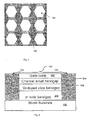
- Fig. 1 illustrates a relative arrangement of a hardmask and nano-islands constructed therewith on a silicon substrate in accordance with one embodiment.
- Fig. 2 illustrates a heteroepitaxial layer structure of a nano-island for an n-channel MOSFET in accordance with one embodiment.
- Fig. 3A illustrates a transistor constructed over a nano-island in accordance with one embodiment.
- Fig. 3B illustrates a transistor constructed over traditional materials in accordance with the prior art.
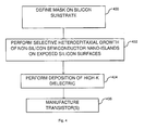
- Fig. 4 illustrates a method of creating dislocation-free, thin heteroepitaxial, single crystal nano-islands on a substrate in accordance with one embodiment.
- Fig. 5 illustrates a graph of historic and projected sizes for various types of logic gate cells.
- the embodiments described herein provide a low-defect or defect-free heteroepitaxial approach compatible with CMOS requirements, including, but not limited to, effective heat removal and planarity, as well compatibility with existing CMOS manufacturing methods at and below the 22 nm node.
- the embodiments described herein provide dislocation-free heteroepitaxial nano-islands of single crystal material on a silicon substrate.
- Transistors fabricated on the nano-islands are compatible with CMOS manufacturing requirements; in particular, the structure is planar, thin device layers allow for sufficient heat removal, and area requirements are identical to standard silicon CMOS as described in the International Technology Roadmap for Semiconductors. Additionally, the mask used to create the nano-islands on the silicon substrate is simultaneously used to electrically isolate devices from each other.
- a hardmask 100 which may comprise, for example, a dielectric, is used to create dislocation-free, thin heteroepitaxial, single crystal nano-islands 102 on a silicon substrate 200 ( Fig. 2 ), as described in connection with Fig. 4 .
- the nano-islands 102 could be interpreted as terminated nanowires comprising only thin layers required for device functionality. In one embodiment, the total thickness of the nano-islands 102 does not exceed 50 nm.
- the nano-islands 102 may include a number of heteroepitaxial layers as dictated by device requirements.
- Fig. 1 a hardmask 100, which may comprise, for example, a dielectric, is used to create dislocation-free, thin heteroepitaxial, single crystal nano-islands 102 on a silicon substrate 200 ( Fig. 2 ), as described in connection with Fig. 4 .
- the nano-islands 102 could be interpreted as terminated nanowires comprising only thin layers required for device functionality. In one embodiment, the total thickness of the
- FIG. 2 illustrates an n-channel MOSFET layer structure of a single nano-island 102, which includes a gate oxide layer 202, a channel small bandgap layer 204, an undoped wide bandgap layer 206, and a p+ wide bandgap layer 208.
- a gate oxide layer 202 On each nano-island 102, one or multiple transistors can be realized, or nano-islands can be combined to form a larger transistor.
- the size of a nano-island 102 is similar to the typical cross-section of a nanowire and the upper limit of the size of a nano-island dictated by the limitations of dislocation-free growth.
- the hardmask 100 comprises includes hexagonally-shaped openings (hence, the term "honeycomb") to facilitate dislocation-free growth.
- the silicon substrate 200 may further have a (111) surface orientation to facilitate dislocation-free growth.
- the hardmask 100 may be designed such that the area requirement of a transistor implemented using a nano-island is equivalent to a standard CMOS silicon transistor of a given node, as illustrated in Figs. 3A and 3B .
- Fig. 3A illustrates a transistor 300 constructed over a nano-island 302 in accordance with one embodiment.
- FIG. 3B illustrates a transistor 300' constructed over traditional materials, in this case, silicon 302', in accordance with the prior art.
- an area 304 represents a hardmask and isolation.
- an area 304' represents STI and isolation.
- Each of the transistors 300, 300' includes a gate 306, 306', respectively, and ohmic contacts 308, 308', respectively.
- the area of the transistor 300 is essentially equivalent to that of the transistor 300'.
- Fig. 4 illustrates a flowchart of a method of creating dislocation-free, thin heteroepitaxial, single crystal nano-islands on a substrate in accordance with one embodiment.
- a mask is defined on a silicon substrate using, for example, thermal oxidation, oxide deposition, and/or lithography. As described in connection with Fig. 1 , the mask defined in step 400 is a hardmask.
- step 402 selective heteroepitaxial growth of non-silicon semiconductor nano-islands onto exposed silicon surfaces is performed, for example, via metalorganic chemical vapor deposition ("MOCVD") and/or gas source molecular beam epitaxy ("MBE").
- MOCVD metalorganic chemical vapor deposition
- MBE gas source molecular beam epitaxy
- step 404 high-k gate dielectric is deposited, for example, via MOCVD, atomic layer deposition ("ALD”), and/or MBE.
- step 406 transistors are constructed over the nano-islands by placing gates, sidewalls, and ohmic contacts thereof.
- Non-silicon channel materials such as III-V semiconductors and Ge, are considered for CMOS generations beyond 22 nm.
- Typical transistor area for such technologies is ⁇ 20,000 nm 2 .
- Fig. 5 illustrates a graph of historic and projected sizes for MPU gate size (4 transistors).
- the projected size for a single transistor for the 16 and 11 nm nodes is about 20,000 nm 2 and 10,000 nm 2 including isolation, as indicated by points 500 and 501, respectively. This translates into edge length of 140 and 100 nm, assuming a transistor cell of square area and including isolation. Note that the nano-islands of heteroepitaxial material are still smaller since they are implemented inside the isolation mask pattern. Dislocation-free InAs nanowires on silicon substrate with such dimensions have already been demonstrated.
Landscapes
- Insulated Gate Type Field-Effect Transistor (AREA)
- Recrystallisation Techniques (AREA)
- Metal-Oxide And Bipolar Metal-Oxide Semiconductor Integrated Circuits (AREA)
- Non-Volatile Memory (AREA)
- Semiconductor Memories (AREA)
- Element Separation (AREA)
Applications Claiming Priority (1)
| Application Number | Priority Date | Filing Date | Title |
|---|---|---|---|
| US12/562,852 US20110068368A1 (en) | 2009-09-18 | 2009-09-18 | Semiconductor device comprising a honeycomb heteroepitaxy |
Publications (2)
| Publication Number | Publication Date |
|---|---|
| EP2299490A2 true EP2299490A2 (de) | 2011-03-23 |
| EP2299490A3 EP2299490A3 (de) | 2013-11-20 |
Family
ID=43303897
Family Applications (1)
| Application Number | Title | Priority Date | Filing Date |
|---|---|---|---|
| EP10006435.1A Withdrawn EP2299490A3 (de) | 2009-09-18 | 2010-06-21 | Halbleiterbauelement mit Wabenheteroepitaxie |
Country Status (6)
| Country | Link |
|---|---|
| US (1) | US20110068368A1 (de) |
| EP (1) | EP2299490A3 (de) |
| JP (2) | JP2011066410A (de) |
| KR (1) | KR101345897B1 (de) |
| CN (1) | CN102024759B (de) |
| TW (1) | TWI484564B (de) |
Cited By (1)
| Publication number | Priority date | Publication date | Assignee | Title |
|---|---|---|---|---|
| US9450007B1 (en) | 2015-05-28 | 2016-09-20 | Stmicroelectronics S.R.L. | Integrated circuit with reflective material in trenches and related methods |
Family Cites Families (20)
| Publication number | Priority date | Publication date | Assignee | Title |
|---|---|---|---|---|
| US5238869A (en) * | 1988-07-25 | 1993-08-24 | Texas Instruments Incorporated | Method of forming an epitaxial layer on a heterointerface |
| JPH04315419A (ja) * | 1991-04-12 | 1992-11-06 | Nec Corp | 元素半導体基板上の絶縁膜/化合物半導体積層構造 |
| JP3660897B2 (ja) * | 2001-09-03 | 2005-06-15 | 株式会社ルネサステクノロジ | 半導体装置の製造方法 |
| US7087480B1 (en) * | 2002-04-18 | 2006-08-08 | Taiwan Semiconductor Manufacturing Company, Ltd. | Process to make high-k transistor dielectrics |
| US6730576B1 (en) * | 2002-12-31 | 2004-05-04 | Advanced Micro Devices, Inc. | Method of forming a thick strained silicon layer and semiconductor structures incorporating a thick strained silicon layer |
| JP2004336040A (ja) * | 2003-04-30 | 2004-11-25 | Osram Opto Semiconductors Gmbh | 複数の半導体チップの製造方法および電子半導体基体 |
| JP2005011915A (ja) * | 2003-06-18 | 2005-01-13 | Hitachi Ltd | 半導体装置、半導体回路モジュールおよびその製造方法 |
| US7037849B2 (en) * | 2003-06-27 | 2006-05-02 | Taiwan Semiconductor Manufacturing Company, Ltd. | Process for patterning high-k dielectric material |
| US7037770B2 (en) * | 2003-10-20 | 2006-05-02 | International Business Machines Corporation | Method of manufacturing strained dislocation-free channels for CMOS |
| US6864540B1 (en) * | 2004-05-21 | 2005-03-08 | International Business Machines Corp. | High performance FET with elevated source/drain region |
| US7105889B2 (en) * | 2004-06-04 | 2006-09-12 | International Business Machines Corporation | Selective implementation of barrier layers to achieve threshold voltage control in CMOS device fabrication with high k dielectrics |
| US20060292719A1 (en) * | 2005-05-17 | 2006-12-28 | Amberwave Systems Corporation | Lattice-mismatched semiconductor structures with reduced dislocation defect densities and related methods for device fabrication |
| US9153645B2 (en) * | 2005-05-17 | 2015-10-06 | Taiwan Semiconductor Manufacturing Company, Ltd. | Lattice-mismatched semiconductor structures with reduced dislocation defect densities and related methods for device fabrication |
| CN101268547B (zh) * | 2005-07-26 | 2014-07-09 | 琥珀波系统公司 | 包含交替有源区材料的结构及其形成方法 |
| JP4885507B2 (ja) * | 2005-10-05 | 2012-02-29 | 古河機械金属株式会社 | Iii族窒化物半導体層の形成方法、iii族窒化物半導体基板の製造方法 |
| KR101019941B1 (ko) * | 2006-03-10 | 2011-03-09 | 에스티씨. 유엔엠 | Gan 나노선의 펄스 성장 및 ⅲ 족 질화물 반도체 기판 물질과 디바이스에서의 어플리케이션 |
| CN101443887B (zh) * | 2006-03-10 | 2011-04-20 | Stc.Unm公司 | Gan纳米线的脉冲式生长及在族ⅲ氮化物半导体衬底材料中的应用和器件 |
| US7777250B2 (en) * | 2006-03-24 | 2010-08-17 | Taiwan Semiconductor Manufacturing Company, Ltd. | Lattice-mismatched semiconductor structures and related methods for device fabrication |
| KR100810983B1 (ko) * | 2006-05-11 | 2008-03-10 | 재단법인서울대학교산학협력재단 | 위치 선택적 수직형 나노선 성장 방법, 수직형 나노선을포함하는 반도체 나노 소자 및 이의 제조 방법 |
| EP2058844A1 (de) * | 2007-10-30 | 2009-05-13 | Interuniversitair Microelektronica Centrum (IMEC) | Herstellungsverfahren für eine Halbleitervorrichtung |
-
2009
- 2009-09-18 US US12/562,852 patent/US20110068368A1/en not_active Abandoned
- 2009-12-22 TW TW098144136A patent/TWI484564B/zh active
-
2010
- 2010-01-20 CN CN201010004651XA patent/CN102024759B/zh active Active
- 2010-06-21 EP EP10006435.1A patent/EP2299490A3/de not_active Withdrawn
- 2010-06-29 KR KR1020100061926A patent/KR101345897B1/ko active Active
- 2010-09-13 JP JP2010203889A patent/JP2011066410A/ja active Pending
-
2014
- 2014-07-11 JP JP2014143317A patent/JP2014225681A/ja active Pending
Non-Patent Citations (3)
| Title |
|---|
| C. THELANDER ET AL.: "Vertical Enhancement-Mode InAs Nanowire Field-Effect Transistor with 50nm Wrap Gate", ELECTRON DEVICE LETTERS, vol. 29, no. 3, 2008, pages 206, XP011203179 |
| Q.T. DO ET AL.: "High Transconductance MISFET with a Single InAs Nanowire Channel", ELECTRON DEVICE LETTERS, vol. 28, no. 8, 2007, pages 682, XP011189093, DOI: doi:10.1109/LED.2007.902082 |
| T. MARTENSSON ET AL., ADVANCED MATERIALS, vol. 19, 2007, pages 1801 - 1806 |
Cited By (2)
| Publication number | Priority date | Publication date | Assignee | Title |
|---|---|---|---|---|
| US9450007B1 (en) | 2015-05-28 | 2016-09-20 | Stmicroelectronics S.R.L. | Integrated circuit with reflective material in trenches and related methods |
| US9773930B2 (en) | 2015-05-28 | 2017-09-26 | Stmicroelectronics S.R.L. | Integrated circuit with reflective material in trenches and related methods |
Also Published As
| Publication number | Publication date |
|---|---|
| CN102024759A (zh) | 2011-04-20 |
| JP2014225681A (ja) | 2014-12-04 |
| EP2299490A3 (de) | 2013-11-20 |
| JP2011066410A (ja) | 2011-03-31 |
| KR20110031080A (ko) | 2011-03-24 |
| US20110068368A1 (en) | 2011-03-24 |
| KR101345897B1 (ko) | 2013-12-30 |
| CN102024759B (zh) | 2013-05-29 |
| TWI484564B (zh) | 2015-05-11 |
| TW201112335A (en) | 2011-04-01 |
Similar Documents
| Publication | Publication Date | Title |
|---|---|---|
| US10074536B2 (en) | Lattice-mismatched semiconductor structures and related methods for device fabrication | |
| TWI660509B (zh) | Channel field effect transistor and switching element | |
| KR101225816B1 (ko) | 감소한 변위 결함 밀도를 가지는 래티스 미스매칭된 반도체구조 및 디바이스 제조를 위한 관련 방법 | |
| US11374106B2 (en) | Method of making heteroepitaxial structures and device formed by the method | |
| TWI656638B (zh) | 用於iii-v族奈米線穿隧fet之方法及結構 | |
| WO2015064094A1 (ja) | Iii-v族化合物半導体ナノワイヤ、電界効果トランジスタおよびスイッチ素子 | |
| US20240363344A1 (en) | Epitaxies of a Chemical Compound Semiconductor | |
| CN109872943B (zh) | 形成用于半导体结构的方法以及由该方法制造的半导体结构 | |
| EP2299490A2 (de) | Halbleiterbauelement mit Wabenheteroepitaxie | |
| CN102214685A (zh) | 具有悬空源漏的半导体结构及其形成方法 | |
| CN102790006B (zh) | 半导体结构及其制作方法 | |
| TW202005090A (zh) | 穿隧場效電晶體裝置 | |
| EP3465737A2 (de) | Verfahren zur herstellung komplementärer vorrichtungen |
Legal Events
| Date | Code | Title | Description |
|---|---|---|---|
| PUAI | Public reference made under article 153(3) epc to a published international application that has entered the european phase |
Free format text: ORIGINAL CODE: 0009012 |
|
| AK | Designated contracting states |
Kind code of ref document: A2 Designated state(s): AL AT BE BG CH CY CZ DE DK EE ES FI FR GB GR HR HU IE IS IT LI LT LU LV MC MK MT NL NO PL PT RO SE SI SK SM TR |
|
| AX | Request for extension of the european patent |
Extension state: BA ME RS |
|
| PUAL | Search report despatched |
Free format text: ORIGINAL CODE: 0009013 |
|
| RIC1 | Information provided on ipc code assigned before grant |
Ipc: H01L 21/8258 20060101ALI20130927BHEP Ipc: H01L 27/02 20060101AFI20130927BHEP Ipc: H01L 21/20 20060101ALI20130927BHEP Ipc: H01L 27/06 20060101ALI20130927BHEP |
|
| AK | Designated contracting states |
Kind code of ref document: A3 Designated state(s): AL AT BE BG CH CY CZ DE DK EE ES FI FR GB GR HR HU IE IS IT LI LT LU LV MC MK MT NL NO PL PT RO SE SI SK SM TR |
|
| AX | Request for extension of the european patent |
Extension state: BA ME RS |
|
| STAA | Information on the status of an ep patent application or granted ep patent |
Free format text: STATUS: THE APPLICATION IS DEEMED TO BE WITHDRAWN |
|
| 18D | Application deemed to be withdrawn |
Effective date: 20140125 |