EP2293092B1 - Elément de détection de magnéto-impédance - Google Patents
Elément de détection de magnéto-impédance Download PDFInfo
- Publication number
- EP2293092B1 EP2293092B1 EP09762477.9A EP09762477A EP2293092B1 EP 2293092 B1 EP2293092 B1 EP 2293092B1 EP 09762477 A EP09762477 A EP 09762477A EP 2293092 B1 EP2293092 B1 EP 2293092B1
- Authority
- EP
- European Patent Office
- Prior art keywords
- sensor element
- wire
- base body
- magnetic amorphous
- amorphous wire
- Prior art date
- Legal status (The legal status is an assumption and is not a legal conclusion. Google has not performed a legal analysis and makes no representation as to the accuracy of the status listed.)
- Active
Links
- 239000012212 insulator Substances 0.000 claims description 27
- 239000011248 coating agent Substances 0.000 claims description 24
- 238000000576 coating method Methods 0.000 claims description 24
- 239000000758 substrate Substances 0.000 claims description 16
- 230000000630 rising effect Effects 0.000 claims description 2
- 235000012431 wafers Nutrition 0.000 description 27
- 238000005549 size reduction Methods 0.000 description 26
- 230000000052 comparative effect Effects 0.000 description 21
- 238000005520 cutting process Methods 0.000 description 14
- 230000001965 increasing effect Effects 0.000 description 14
- 230000035945 sensitivity Effects 0.000 description 14
- 239000000463 material Substances 0.000 description 11
- 238000003754 machining Methods 0.000 description 8
- 238000004519 manufacturing process Methods 0.000 description 8
- 238000000034 method Methods 0.000 description 7
- 239000000919 ceramic Substances 0.000 description 4
- 238000001514 detection method Methods 0.000 description 4
- 239000003822 epoxy resin Substances 0.000 description 3
- 230000001939 inductive effect Effects 0.000 description 3
- 239000011810 insulating material Substances 0.000 description 3
- 230000003071 parasitic effect Effects 0.000 description 3
- 229920000647 polyepoxide Polymers 0.000 description 3
- 238000012545 processing Methods 0.000 description 3
- 230000003245 working effect Effects 0.000 description 3
- 230000001413 cellular effect Effects 0.000 description 2
- 238000009833 condensation Methods 0.000 description 2
- 230000005494 condensation Effects 0.000 description 2
- 230000007547 defect Effects 0.000 description 2
- 238000011161 development Methods 0.000 description 2
- 230000018109 developmental process Effects 0.000 description 2
- 230000000694 effects Effects 0.000 description 2
- 238000011156 evaluation Methods 0.000 description 2
- 238000007747 plating Methods 0.000 description 2
- 229910000679 solder Inorganic materials 0.000 description 2
- 238000004544 sputter deposition Methods 0.000 description 2
- 229910019230 CoFeSiB Inorganic materials 0.000 description 1
- VYPSYNLAJGMNEJ-UHFFFAOYSA-N Silicium dioxide Chemical compound O=[Si]=O VYPSYNLAJGMNEJ-UHFFFAOYSA-N 0.000 description 1
- XUIMIQQOPSSXEZ-UHFFFAOYSA-N Silicon Chemical compound [Si] XUIMIQQOPSSXEZ-UHFFFAOYSA-N 0.000 description 1
- 239000000853 adhesive Substances 0.000 description 1
- 230000001070 adhesive effect Effects 0.000 description 1
- 229910045601 alloy Inorganic materials 0.000 description 1
- 239000000956 alloy Substances 0.000 description 1
- PNEYBMLMFCGWSK-UHFFFAOYSA-N aluminium oxide Inorganic materials [O-2].[O-2].[O-2].[Al+3].[Al+3] PNEYBMLMFCGWSK-UHFFFAOYSA-N 0.000 description 1
- 239000004020 conductor Substances 0.000 description 1
- 230000003247 decreasing effect Effects 0.000 description 1
- 230000001419 dependent effect Effects 0.000 description 1
- 230000002542 deteriorative effect Effects 0.000 description 1
- 238000010586 diagram Methods 0.000 description 1
- 229910052751 metal Inorganic materials 0.000 description 1
- 239000002184 metal Substances 0.000 description 1
- TWNQGVIAIRXVLR-UHFFFAOYSA-N oxo(oxoalumanyloxy)alumane Chemical compound O=[Al]O[Al]=O TWNQGVIAIRXVLR-UHFFFAOYSA-N 0.000 description 1
- 238000004806 packaging method and process Methods 0.000 description 1
- 238000012856 packing Methods 0.000 description 1
- 230000002093 peripheral effect Effects 0.000 description 1
- 229920005989 resin Polymers 0.000 description 1
- 239000011347 resin Substances 0.000 description 1
- 239000004065 semiconductor Substances 0.000 description 1
- 229910052710 silicon Inorganic materials 0.000 description 1
- 239000010703 silicon Substances 0.000 description 1
- 229910052814 silicon oxide Inorganic materials 0.000 description 1
- 239000010409 thin film Substances 0.000 description 1
- 238000004804 winding Methods 0.000 description 1
Images


Classifications
-
- G—PHYSICS
- G01—MEASURING; TESTING
- G01R—MEASURING ELECTRIC VARIABLES; MEASURING MAGNETIC VARIABLES
- G01R33/00—Arrangements or instruments for measuring magnetic variables
- G01R33/02—Measuring direction or magnitude of magnetic fields or magnetic flux
-
- G—PHYSICS
- G01—MEASURING; TESTING
- G01R—MEASURING ELECTRIC VARIABLES; MEASURING MAGNETIC VARIABLES
- G01R33/00—Arrangements or instruments for measuring magnetic variables
- G01R33/02—Measuring direction or magnitude of magnetic fields or magnetic flux
- G01R33/06—Measuring direction or magnitude of magnetic fields or magnetic flux using galvano-magnetic devices
- G01R33/063—Magneto-impedance sensors; Nanocristallin sensors
-
- G—PHYSICS
- G01—MEASURING; TESTING
- G01R—MEASURING ELECTRIC VARIABLES; MEASURING MAGNETIC VARIABLES
- G01R33/00—Arrangements or instruments for measuring magnetic variables
- G01R33/12—Measuring magnetic properties of articles or specimens of solids or fluids
- G01R33/18—Measuring magnetostrictive properties
-
- H—ELECTRICITY
- H10—SEMICONDUCTOR DEVICES; ELECTRIC SOLID-STATE DEVICES NOT OTHERWISE PROVIDED FOR
- H10N—ELECTRIC SOLID-STATE DEVICES NOT OTHERWISE PROVIDED FOR
- H10N50/00—Galvanomagnetic devices
Definitions
- the present invention relates to a magneto-impedance sensor element using a magnetic amorphous wire whose properties change according to an external magnetic field.
- MI sensor elements magneto-impedance sensor elements using magnetic amorphous wires whose properties change according to an external magnetic field
- Such an MI sensor element has a base body composed of a nonmagnetic body, a magnetic amorphous wire held onto the base body, a coating insulator through which the magnetic amorphous wire passes, and a detecting coil formed around the coating insulator.
- the MI sensor element having such a constitution is mounted to portable terminal devices such as cellular phones, size-reduction of the MI sensor element is demanded according to size-reduction and thickness-reduction of such devices.
- Patent Document 1 International Publication No. 2005/008268
- the magnetic amorphous wire is requiredto have certain degree of length.
- a longitudinal direction of the magnetic amorphous wire may be made to conform to a normal direction of a main surface of the IC chip and the IC substrate (Z axial direction).
- the MI sensor element becomes larger in a thickness direction of the IC chip.
- the thinning of the devices becomes difficult.
- the length of the magnetic amorphous wire is preferably equivalent to the entire length of the MI sensor element in the longitudinal direction.
- the wafer is cut so that individual MI sensors are obtained (see FIGS. 5 and 6 in a first embodiment).
- An electrode terminal or the like is not basically formed on the cut surface as a pattern.
- To form the pattern on the cut surface means to form the pattern on the respective MI sensor elements after cutting, and this is not realistic from a viewpoint of productivity. If the pattern is formed on the respective MI sensors, the productivity is reduced significantly as compared with the case where the pattern is formed on the base body wafers.
- a groove is formed on a position of the base body wafer corresponding to a side of the base body perpendicular to the magnetic amorphous wire.
- the electrode terminals are formed on a part of this groove by using sputtering, plating or the like. Thereafter, the base body wafer is cut by a dicing saw or the like so that the electrode terminals formed on the part of the groove are not chipped, and the individual MI sensor elements are obtained. As a result, the part of the groove remains and thus the stepped portion is formed.
- the MI sensor element cannot be allowed to protrude from the base body to the longitudinal direction, its one end portion is arranged on an inner side of the base body with respect to the stepped portion. For this reason, the length of the magnetic amorphous wire should be shorter than the length of the base body by at least a height of the stepped portion, and thus the sensitivity of the MI sensor element is reduced.
- the thickness should be increased in order to secure strength of the base body, and thus the sizes-reduction of the MI sensor becomes difficult.
- a material with comparatively low strength is used for the base body in order to facilitate the cutting work.
- the thickness of the base body should be increased accordingly, and thus the sizes-reduction of the MI sensor element becomes more difficult.
- the electrode terminals are formed on the same surface of the base body as the magnetic amorphous wire is formed, the above problem does not arise.
- a magnetically sensitive direction of the MI sensor element is a direction (Z axial direction) perpendicular to the IC chip, the electrode terminals are not provided to this surface. This is because the electrode terminals should be subject to a process such as wire bonding between them and the electrode terminals on the IC chip, and thus the surface where the IC chip is formed should be basically parallel with the surface where the electrode terminals are formed.
- the present invention is devised from these conventional problems, and its object is to provide a magneto-impedance sensor element that achieves high sensitivity and size-reduction.
- US 2005/0242805 A1 discloses a three-dimensional magnetic direction sensor, and a magneto-impedance sensor element.
- WO 2008/016198 A1 discloses a three axis thin film fluxgate.
- the magneto-impedance sensor element has the terminal base having the terminal mounting surface.
- the terminal mounting surface is arranged between the both ends of the magnetic amorphous wire in the longitudinal direction of the magnetic amorphous wire.
- the wire electrode terminals and the coil electrode terminals can be easily formed on the terminal mounting surface of the terminal base, and the magnetic amorphous wire can be disposed over the base body in the longitudinal direction of the magnetic amorphous wire.
- the magnetic amorphous wire can be lengthened without increasing a size of the base body, and the sensitivity can be heightened without enlarging the MI sensor element.
- the MI sensor element when the MI sensor element is manufactured, in general the magnetic amorphous wire, and the detecting coil and the like are formed on a base body wafer serving as a basic material of the base bodies of many MI sensor elements, and the wafer is cut to obtain individual MI sensor elements.
- the wire electrode terminals and the coil electrode terminals can be easily formed before the individual MI sensor elements are obtained by the cutting.
- the groove does not have to be formed on the base body wafer. For this reason, a problem that the length of the magnetic amorphous wire should be shortened as a stepped portion is formed does not arise, thereby preventing a defect such that the length of the magnetic amorphous wire becomes short with respect to the size of the base body. For this reason, the length of the magnetic amorphous wire can be made to be equivalent to the entire length of the MI sensor element, and thus both the size-reduction and the high sensitivity of the MI sensor element can be achieved.
- the groove machining step is not necessary, the manufacturing cost can be reduced, and the productivity can be improved.
- the thickness of the base body does not particularly have to be increased, and the size-reduction of the MI sensor element becomes easy. Since the facilitating of the cutting work does not particularly have to be considered, a material with high strength can be used as the base body, and accordingly the thickness of the base body can be further decreased, thereby further facilitating the size-reduction of the MI sensor element.
- the magneto-impedance sensor element that achieves high sensitivity and size-reduction can be provided.
- a terminal mounting surface is preferably formed so that its normal is conformed to a longitudinal direction of a magnetic amorphous wire.
- the magnetic amorphous wire is arranged so as to be perpendicular to a main surface of the IC chip, wire electrode terminals and coil electrode terminals can be made to be parallel with the main surface of the IC chip.
- the wire electrode terminals and the coil electrode terminals can be easily electrically connected with the IC chip by wire bonding or the like.
- the terminal base is formed on an area other than the area where the magnetic amorphous wire, a coating insulator and a detecting coil are formed.
- the terminal base does not cover the magnetic amorphous wire, the coating insulator and the detecting coil, a stress to be applied to the magnetic amorphous wire, dew condensation on the magnetic amorphous wire and the like are prevented, and accurate detection of a magnetic field can be secured.
- the terminal base is disposed so as to cover the magnetic amorphous wire, a stress might be applied to the magnetic amorphous wire, and a parasitic capacitance might be changed by the dew condensation or the like of air present between the magnetic amorphous wire and the terminal base.
- An electric current to be supplied to the magnetic amorphous wire fluctuates due to the stress and the change in the parasitic capacitance, and magnetic sensitivity of the MI sensor element (output/applied magnetic field) might vary (for example, the magnetic sensitivity might vary by about 10%).
- the terminal base is provided so as not to cover the magnetic amorphous wire, thereby avoiding such a defect. That is, the variation of the magnetic sensitivity of the MI sensor element can be mostly eliminated (for example, the variation in the magnetic sensitivity is less than 1%).
- the element is packaged to an IC chip formed by an electronic circuit so that a longitudinal direction of the magnetic amorphous wire is conformed to a normal direction of a main surface of the IC chip.
- the wire electrode terminals and the coil electrode terminals do not have the same direction component as the longitudinal direction component of the magnetic amorphous wire, it is difficult to connect the electronic circuit formed on the main surface of the IC chip and the terminals. For this reason, it is not desirable that the wire electrode terminals and the coil electrode terminal are provided on the surface of the base body where the magnetic amorphous wire is formed.
- the wire electrode terminals and the coil electrode terminals are formed on a surface that is at a certain angle or, more preferably, perpendicular to the surface formed with the magnetic amorphous wire is formed.
- the present invention is applied to such an MI sensor element so that the operational effect can be sufficiently exerted.
- the packaging of the MI sensor element to the IC chip includes direct electric connection of the MI sensor element to the IC chip by means of wire bonding or the like, and also indirect electric connection of the IC chip to the MI sensor element via an IC substrate on which the IC chip is installed.
- the element may be packaged to the IC substrate provided with the IC chip mounted thereon with the electronic circuit formed thereon, so that the longitudinal direction of the magnetic amorphous wire is conformed to a normal direction of the main surface of the IC substrate.
- the MI sensor element When the MI sensor element is electrically connected to the IC chip via the IC substrate provided with the IC chip mounted thereon, the MI sensor element is packaged so that the longitudinal direction of the magnetic amorphous wire is conformed to the normal direction of the main surface of the IC substrate. As a result, the terminals of the electronic circuit formed on the main surface of the IC substrate are easily connected to the wire electrode terminals and the coil electrode terminals. In such a constitution, the working-effect of the present invention can be sufficiently exerted.
- the magneto-impedance sensor element according to a first embodiment of the present invention is described with reference to FIGS. 1 to 6 .
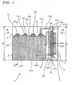
- a magneto-impedance sensor element (MI sensor element) 1 has a base body 2 made of a nonmagnetic body, a magnetic amorphous wire 3 held on the base body 2, a coating insulator 4 formed so that the magnetic amorphous wire 3 passes through its inside, and a detecting coil 5 formed around the coating insulator 4.
- a terminal base 6 made of an insulator having a terminal mounting surface 61 rising from a surface 21 is formed on the surface 21 of the base body 2 on which the magnetic amorphous wire 3 is arranged.
- a pair of wire electrode terminals 11 and a pair of coil electrode terminals 12 are formed on the terminal mounting surface 61.
- One of the paired wire electrode terminals 11 and one of the paired coil electrode terminals 12 can share one electrode as a standard potential. In this case, a total number of the wire electrode terminals 11 and the coil electrode terminals 12 can be three.
- the wire electrode terminals 11 are electrically connected to a pair of wire conducting terminals 31 provided to the magnetic amorphous wire 3 by wire connecting wirings 110.
- the coil electrode terminals 12 are electrically connected to a pair of coil conducting terminals 51 provided to the detecting coil 5 by coil connecting wirings 120.
- the normal of the terminal mounting surface 61 has a direction component same as the longitudinal direction component of the magnetic amorphous wire 3, and the terminal mounting surface 61 is arranged between both ends 311, 311 of the magnetic amorphous wire 3 in the longitudinal direction of the magnetic amorphous wire 3.
- the terminal mounting surface 61 is formed so that its normal is in the longitudinal direction of the magnetic amorphous wire 3.
- the terminal base 6 is formed on an area other than the area where the magnetic amorphous wire 3, the coating insulator 4 and the detecting coil 5 are formed. That is, the terminal base 6 is formed in a position other than the area where the magnetic amorphous wire 3, the coating insulator 4 and the detecting coil 5 are formed so as not to cover them, although the terminal base 6 is formed on the surface of the base body 2 so as to partially cover the wire connecting wirings 110 and the coil connecting wirings 120..
- the MI sensor element 1 in the first embodiment is packaged to the IC chip 7 with an electronic circuit formed, so that the longitudinal direction of the magnetic amorphous wire 3 is conformed to the normal direction of a main surface 71 of an IC chip 7 as shown in FIG. 4 .
- a direction perpendicular to the main surface 71 of the IC chip 7 at the time of packing into the IC chip 7 is a Z axial direction. That is, the direction that corresponds to the longitudinal direction of the magnetic amorphous wire 3 is the Z axial direction.
- a thickness in the direction perpendicular to the main surface 21 can be set to, for example, 0.1 mm to 0.5 mm. In the first embodiment, the thickness is 0.3 mm. A height of the base body 2 in the Z axial direction is 0.6 mm.
- the magnetic amorphous wire 3 is made of CoFeSiB alloy of zero magnetostrictive amorphous, and its diameter can be, for example, 20 ⁇ m or less. In this embodiment, the diameter is 10 ⁇ m.
- the magnetic amorphous wire 3 is disposed on the surface 21 of the base body 2 over the Z axial direction of the base body 2 as shown in FIG. 1 . In this embodiment, a length of the magnetic amorphous wire 3 is 0.6 mm.
- Wire conducting terminals 31 on both ends of the magnetic amorphous wire 3 are electrically connected to conducting pads 310 formed on the surface 21 of the base body 2.
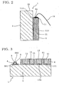
- the coating insulator 4 can be formed by using an inorganic insulating material such as aluminum oxide or silicon oxide or an organic insulating material such as epoxy resin.
- the detecting coil 5 is formed on an outer peripheral surface of the coating insulator 4.
- the detecting coil 5 is disposed so as to be spirally wound around the outer periphery of the coating insulator 4 by suitably connecting a plane pattern 501 deposited on the surface 21 of the base body 2 to a cubic pattern 502 deposited on an outer surface of the coating insulator 4. Both ends of the winding pattern of the detecting coil 5 are coil conducting terminals 51.
- the number of turns of the detecting coil 5 is 15.
- the magnetic amorphous wire 3, the coating insulator 4 and the detecting coil 5 are disposed so as to rise from the surface 21 of the base body 2.
- a groove may be formed on the base body, and the magnetic amorphous wire, the coating insulator and the detection coil may be arranged therein.
- the thickness of the base body must be increased, and thus it is desirable to adopt the constitution of the first embodiment from a viewpoint of the size-reduction.
- each of the coil connecting wirings 120 formed on the surface 21 of the base body 2 is connected to the paired coil conducting terminals 51.
- One end of each of the wire connecting wirings 110 formed on the surface 21 of the base body 2 is connected to the paired wire conducting terminals 31 via the conducting pads 310.
- each of the wire connecting wirings 110 is connected to the wire electrode terminals 11, and the other end of each of the coil connecting wires 120 is connected to the coil electrode terminals 12.
- the terminal base 6 provided to the surface 21 of the base body 2 is made of an insulator such as epoxy resin or ceramic, and is formed so as to cover the wire connecting wirings 110 and the coil connecting wirings 120.
- the terminal base 6 is provided with the terminal mounting surface 61, which is a flat surface perpendicular to the Z axis, in a position that retreats sufficiently inside (by, for example, 150 to 550 ⁇ m) from one end (upper end 22) of the base body 2 in the Z axial direction.
- the terminal mounting surface 61 retreats from the upper end 22 by 200 ⁇ m.
- the paired wire electrode terminals 11 and the paired coil electrode terminals 12 are provided on the terminal mounting surface 61.
- the terminal base 6 is formed on the entire surface 21 of the base body 2 excluding the area where the magnetic amorphous wire 3, the coating insulator 4 and the detecting coil 5 are formed and an area from the terminal mounting surface 61 to the end surface (upper end 22) of the base body 2 in a direction the terminal mounting surface 61 faces.
- a thickness of the terminal base 6, namely, a width of the terminal mounting surface 61 is, for example 80 to 150 ⁇ m. In the first embodiment, the width of the terminal mounting surface 61 is 100 ⁇ m.
- Terminal portions 111 of the wire connecting wirings 110 on the side of the wire electrode terminals 11 are formed to partially protrude from the terminal mounting surface 61 and are connected to the wire electrode terminals 11.
- terminal portions 121 of the coil connecting wirings 120 on the side of the coil electrode terminals 12 are formed so as to partially protrude from the terminal mounting surface 61 and are connected to the coil electrode terminals 12.
- the MI sensor element 1 is packaged to the IC chip 7 as the element for Z axial direction, and is disposed so that the longitudinal direction of the magnetic amorphous wire 3 is perpendicular to the main surface 71 of the IC chip 7.
- the IC chip 7 is installed to an IC substrate 73 for connecting a mother board and the IC chip 7, and a main surface 731 of the IC substrate 73 is parallel with the main surface 71 of the IC chip 7.
- the MI sensor element 1 is installed to the main surface 731 of the IC substrate 73 beside the IC chip 7.
- the wire electrode terminals 11 and the coil electrode terminals 12 in the MI sensor element 1 are electrically connected to predetermined terminals in the electronic circuit formed on the main surface 71 of the IC chip 7 or predetermined terminals in the electronic circuit formed on the main surface 731 of the IC substrate 73, respectively, by bonding wires 72.
- both the two coil electrode terminals 12 in the MI sensor element 1 are bonding-connected to the terminals of the IC chip 7, but one of the wire electrode terminals 11 is bonding-connected to the terminal of the IC chip 7 and the other one is bonding-connected to the terminal of the IC substrate 73.
- This connecting method is one example.
- all the wire electrode terminals 11 and the coil electrode terminals 12 in the MI sensor element 1 may be connected to the terminals of the IC chip 7, or may be connected to the terminals of the IC substrate 73.
- an MI sensor element 10 for an X axis and an MI sensor element 100 for a Y axis which has a magnetic amorphous wire 30 in a direction parallel with the main surface 71 of the IC chip 7 and perpendicular to each other, are packaged to the IC chip 7.
- the MI sensor element 10 for the X axis and the MI sensor element 100 for the Y axis have components approximately similar to those of the MI sensor element 1 for the Z axis of the first embodiment.
- the MI sensor elements 10 and 100 are different from the MI sensor element 1 for the Z axis in that they do not have the terminal base 6 and the wire electrode terminals 11 and the coil electrode terminals 12 are formed on the surface of the base body 2 where the magnetic amorphous wire 30 is provided.
- the three MI sensor elements (1, 10 and 100) including the MI sensor element 1 of the first embodiment compose a magnetic direction sensor 70 for detecting a three-dimensional direction utilizing geomagnetism.
- This geomagnetic direction sensor 70 can be installed to portable terminal devices such as cellular phones.
- the MI sensor element 1 for the Z axial direction according to the first embodiment is combined with the MI sensor elements 10 and 100 for the X axis and Y axis, so as to compose the triaxial magnetic direction sensor 70, but the two MI sensor elements including the MI sensor element 1 according to the first embodiment can compose a biaxial magnetic direction sensor.
- the MI sensor element 1 according to the first embodiment is not limited to such a magnetic direction sensor, and can be used for a current sensor or the like. In this case, only the one MI sensor element 1 according to the first embodiment is used to compose the sensor.
- the magnetic amorphous wire 3, the detecting coil 5 and the like are formed on a base body wafer 20 serving as the basic material of the base body 2 of the many MI sensor elements 1. That is, the many MI sensor elements 1 (for example, the size of about 1 mm or less square) is formed on the large base body wafer 20 of about 10 cm square as a pattern.
- the terminal base 6 is formed on the surface 21 of the base body 2.
- photosensitive epoxy resin for example, can be used. That is, after being applied to the entire surface 21 of the base body 2, the resin is dried and exposed in a state where it is masked so that light is emitted only to a portion where the terminal base 6 is desired to be formed. Development is performed by a developer, so that the terminal base 6 having predetermined size and shape is formed on a predetermined position.
- the wire electrode terminals 11 and the coil electrode terminals 12 are deposited on the terminal mounting surface 61 of the terminal base 6 by using sputtering or plating.
- the base body wafer 20 is cut by using a dicing saw, so that individual MI sensor elements 1 are obtained.
- the cut surface is made to be a desired outline of the MI sensor element 1, taking into account a cutting margin 201 (for example, 200 ⁇ m) of the dicing saw.
- the magneto-impedance sensor element 1 has the terminal base 6 having the terminal mounting surface 61, and the terminal mounting surface 61 is arranged between both ends 311, 311 of the magnetic amorphous wire 3 in the longitudinal direction of the magnetic amorphous wire 3.
- the wire electrode terminals 11 and the coil electrode terminals 12 can be easily formed on the terminal mounting surface 61 of the terminal base 6, and the magnetic amorphous wire 3 can be disposed over the entire base body 2 in the longitudinal direction of the magnetic amorphous wire 3.
- the magnetic amorphous wire 3 can be lengthened without increasing the size of the base body 2, and the sensitivity can be heightened without enlarging the MI sensor element 1.
- the base body wafer 20 is cut so that individual MI sensor elements 1 are obtained.
- the wire electrode terminals 11 and the coil electrode terminals 12 can be easily formed before the individual MI sensor elements 1 are obtained by the cutting.
- the MI sensor element 1 has the terminal base 6, the groove described in a comparative example (see reference symbol 99 in FIG. 14(A) ) does not have to be formed on the base body wafer 20. For this reason, the length of the magnetic amorphous wire 3 can be made to be equivalent to the entire length of the MI sensor element 1, and both the size-reduction and the high sensitivity of the MI sensor element 1 can be achieved.
- the groove machining step is not necessary, the manufacturing cost can be reduced, and the productivity can be improved.
- the thickness of the base body 2 does not have to be particularly increased, thereby facilitating the size-reduction of the MI sensor element 1. Further, since the facilitation of the cutting work does not have to be particularly taken into consideration, a material with high strength can be used for the base body 2. Accordingly, the thickness of the base body 2 can be further reduced, and thus the size-reduction of the MI sensor element 1 becomes easier.
- the terminal base 6 is formed on the area other than the area where the magnetic amorphous wire 3, the coating insulator 4 and the detecting coil 5 are formed. As a result, the terminal base 6 does not cover the magnetic amorphous wire 3, the coating insulator 4 and the detecting coil 5, thereby preventing the stress from being applied to the magnetic amorphous wire 3 and securing accurate detection of the magnetic field.
- the magneto-impedance sensor element that achieves high sensitivity and size-reduction can be provided.
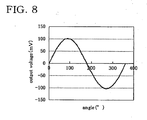
- a characteristic evaluation conducted on the MI sensor element 1 according to the first embodiment is described below with reference to FIGS. 7 and 8 .
- the MI sensor element 1 is incorporated into an electronic circuit 8 shown in FIG. 7 , and the following magnetic sensing evaluation was conducted.
- the electronic circuit 8 has a pulse oscillating circuit 81 for oscillating a pulse signal to be input into the magnetic amorphous wire 3 of the MI sensor element 1, and a signal processing circuit 82 for processing a detection voltage generated on the detecting coil 5 of the MI sensor element 1.
- the signal processing circuit 82 has an analog switch 821 for switching between the detecting coil 5 and an output terminal 83, a sample timing adjusting circuit 822 for turning on/off the analog switch 821 in conjunction with a pulse signal, and an amplifier 823 for amplifying an inductive voltage generated on the detecting coil 5.
- the pulse oscillating circuit 81 generates a pulse signal mainly including 200 MHz, whose intensity is 170 mA and whose signal interval is 1 ⁇ sec, and inputs this pulse signal into the magnetic amorphous wire 3.
- a cutoff time at which the pulse current falls from 90% of a steady state value to 10% is set to 4 nanoseconds.
- the inductive voltage according to a magnetic field in the longitudinal direction (Z axial direction) of the magnetic amorphous wire 3 is generated on the detecting coil 5 of the MI sensor element 1 at the time of falling of the pulse signal.
- This inductive voltage is amplified by the amplifier 823 via the analog switch 821 so as to be outputted from the output terminal 83.
- a state that the longitudinal direction (Z axial direction) of the magnetic amorphous wire 3 of the MI sensor element 1 is conformed to a vertical direction is defined as being a rotation angle of 0°, and the intensity of the output signal of the MI sensor element 1 is 0 mV.
- the MI sensor element 1 is rotated around the horizontal axis by 360°. A change in the output signal at this time is shown in FIG. 8 .
- the output signal draws a beautiful sine curve, and a component of the Z axial direction of geomagnetism is accurately detected.
- the MI sensor element 1 in the first embodiment can secure sufficient detecting accuracy even if its size is reduced.
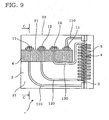
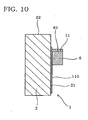
- a second embodiment is an example where the size of the terminal base 6 is reduced in comparison with the first embodiment as shown in FIGS. 9 and 10 .
- the height of the terminal base 6 in the Z axial direction is reduced.
- the height of the terminal base 6 in the MI sensor element 1 according to the first embodiment is 0.4 mm
- the height of the terminal base 6 in the MI sensor element 1 according to the second embodiment is 0.13 mm.
- the terminal base 6 when the terminal mounting surface 61 to which the wire electrode terminals 11 and the coil electrode terminal 12 are mounted can be sufficiently secured, the working-effect of the present invention can be sufficiently obtained. For this reason, the surface 21 of the base body 2 does not have to be a large area unlike the first embodiment. As long as adhesion to the base body 2 is not deteriorated, the terminal base 6 may have various forms in a state where the area of the terminal mounting surface 61 is sufficiently maintained.
- the individual terminal bases may be formed correspondingly to the wire electrode terminals 11 and the coil electrode terminals 12, or the terminal base may be formed into a stepped shape.
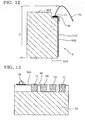
- This example is, as shown in FIGS. 11 to 13 , an example of a magneto-impedance sensor element 9 where the wire electrode terminals 11 and the coil electrode terminals 12 are provided directly to a base body 92 without providing the terminal base 6 described in the first and second embodiments.
- the MI sensor element 9 of the comparative example is formed so that a magnetic amorphous wire 93, the coating insulator 4, the detecting coil 5, the wire connecting wirings 110 and the coil connecting wirings 120 are formed on a surface 921 of the base body 92 similarly to the first and second embodiments.
- One end of the magnetic amorphous wire 93 on the base body 92 in the longitudinal direction (Z axial direction) has a stepped portion 96, and the wire electrode terminals 11 and the coil electrode terminals 12 are provided on a surface perpendicular to the Z axial direction.
- the stepped portion 96 is formed on the entire surface of the base body 92 in a direction perpendicular to the Z axial direction and a thickness direction (a right-left direction of FIG. 11 ).
- the constitution of the construct composed of the magnetic amorphous wire 93, the coating insulator 4 and the detecting coil 5 is similar to that in the first embodiment, and its size and the number of turns of the detecting coil 5 are also similar.
- the stepped portion 96 is necessarily formed, from a viewpoint of the manufacturing, on the MI sensor element 9 for the Z axial direction where the wire electrode terminals 11 and the coil electrode terminals 12 should be formed on the surface perpendicular to the magnetic amorphous wire 3.
- the many MI sensor elements 9 are formed on the base body wafer 920 serving as the basic material of the base bodies 92 of the many MI sensor elements 9. Thereafter, as shown in FIG. 14(B) , the base body wafer 920 is cut by a dicing saw 98 into the individual MI sensor elements 9.
- a groove 99 is formed along a cutting line, which is to be cut, on the surface of the base body wafer 920 before cutting. That is, for example, the groove 99 having a depth of 200 ⁇ m and a width of 200 ⁇ m is formed on the base body wafer 920 as shown in FIG. 14A . Thereafter, the wire electrode terminals 11 and the coil electrode terminals 12 are formed on an inside surface 991 of the groove 99 and on the surface 921 of the base body 92 continuous to 991 as a pattern. Cutting is performed by the dicing saw 98 on a portion slightly outer side (for example, 70 ⁇ m) with respect to the inside surface 991 of the groove 99. As a result, the wire electrode terminals 11 and the coil electrode terminals 12 can be formed on the inside surface 991 of the groove 99 as a pattern in the state before the cutting.
- the base body wafer 920 is cut after the machining of the groove because integrity of the base body wafer 920 is maintained until the forming of the wire electrode terminals 11 and the coil electrode terminals 12 is completed.
- the MI sensor element 9 for the Z axial direction should be provided with the wire electrode terminals 11 and the coil electrode terminals 12 formed on the surface perpendicular to the magnetic amorphous wire 93 as described above. For this reason, the surface perpendicular to the surface 921 of the base body 92 should be formed on the base body 92. For this reason, if the groove is not machined, the wire electrode terminals 11 and the coil electrode terminals 12 cannot be formed on the base body wafer 920. If the groove is not machined, electrode terminals should be formed on the individual cutoff base bodies 2, thereby noticeably deteriorating the productivity. For this reason, the groove is machined so that the electrode terminals can be formed and also the integrity of the base body wafer 920 can be maintained.
- the length of the magnetic amorphous wire 93 should be shorter than the length of the base body 92 in the Z axial direction.
- the magnetic amorphous wire 93 is made to be shorter than the base body 92 by 70 ⁇ m or more.
- a length L of the magnetic amorphous wire 93 ( FIG. 11 ) is significantly shorter than an occupancy height H ( FIG. 12 ) of the MI sensor element 9 in the Z axial direction including the bonding wires 72.
- the groove In order to form the stepped portion 96 on the base body 92 so that the wire electrode terminals 11 and the coil electrode terminals 12 are arranged, the groove should be machined. As a result, the manufacturing cost becomes high, and the thickness should be increased in order to secure the strength of the base body 92.
- a material that is easily machined should be selected as the base body 92 in order to machine the groove on the base body 92, but such a material has weak mechanical strength, and thus the thickness of the base body 92 should be further increased.
- the thickness of the MI sensor element 9 should be increased.
- the length of the magnetic amorphous wire 3 can be made to be as long as the length of the base body 2 in the Z axial direction. For this reason, the length of the magnetic amorphous wire 3 is made to be long, and simultaneously the sizes of the MI sensor element 1 can be reduced.
- the MI sensor element 1 of the present invention does not require the machining of the groove, the thickness of the base body 2 does not have to be large, so the size of the MI sensor element further can be reduced.
- a ratio of the occupancy height H of the MI sensor element in the Z axial direction including the bonding wires to the length L of the magnetic amorphous wire (H/L) is used as a size-reduction index ⁇ of the MI sensor element, and the MI sensor element 1 according to the first embodiment is compared with the MI sensor element 9 of the comparative example.
- the size-reduction index ⁇ is smaller (closer to 1), the size-reduction with an equivalent performance is further achieved.
- the size-reduction index ⁇ of the MI sensor element 9 of the comparative example is calculated.
- a height from a lower end 923 of the base body 92 of the MI sensor element 9 in the comparative example in the Z axial direction to the stepped portion 96 is 0.6 mm, and a height from the stepped portion 96 to the upper end 922 is 0.07 mm.
- a height from the stepped portion 96 to the bonding wires 72 in the Z axial direction is 0.15 mm.
- the bonding wires 72 are positioned below the upper end 22 of the base body 2.
- the occupancy height H ( FIG. 1 ) in the Z axial direction corresponds to the height of the base body 2 in the Z axial direction and is 0.6 mm.
- the magnetic amorphous wire 3 is formed over the entire length of the base body 2 in the Z axial direction, its length L is 0.6 mm.
- the MI sensor element according to the first embodiment realizes the size-reduction of 20% in the Z axial direction with respect to the MI sensor element of the comparative example. That is, the length of the magnetic amorphous wire, namely, the magnetic sensitivity is maintained, and simultaneously the size-reduction of 20% in the Z axial direction can be realized.
- the MI sensor element 1 according to the first embodiment is smaller than the MI sensor element 9 of the comparative example.
- the size-reduction index ⁇ of the MI sensor element 9 of the comparative example is 0.67 mm/0.6 mm ⁇ 1.12
- the size-reduction of about 10% can be realized.
- the MI sensor element 9 of the comparative example requires the groove machining as described above, ceramics having weak strength that can be easily cut is used as a material of the base body 92. For this reason, its thickness (the thickness of the base body 92 in a direction perpendicular to the surface 921 where the magnetic amorphous wire 93 is arranged) is set to as thick as 0.5 mm.
- the thickness of the base body 2 is set to 0.3 mm. Even when the thickness (0.1 mm) of the terminal base 6 is added, the thickness of the MI sensor element 1 becomes 0.4 mm. That is, also the thickness of the MI sensor element according to the first embodiment can be thinner than that in the comparative example.
- the size-reduction index ⁇ of the MI sensor element as the ratio (H/L) of the occupancy height H of the MI sensor element in the Z axial direction including the bonding wires to the length L of the magnetic amorphous wire finally becomes large. That is, in this case, when the length L of the magnetic amorphous wire is 0.60 mm, the occupancy height H of the MI sensor element in the Z axial direction including the bonding wires becomes as long as 0.75 mm.
Landscapes
- Physics & Mathematics (AREA)
- Condensed Matter Physics & Semiconductors (AREA)
- General Physics & Mathematics (AREA)
- Chemical & Material Sciences (AREA)
- Engineering & Computer Science (AREA)
- Nanotechnology (AREA)
- Measuring Magnetic Variables (AREA)
- Hall/Mr Elements (AREA)
Claims (4)
- Élément capteur de magnéto-impédance, comprenant
un corps (2) de base fait d'un corps non-magnétique ;
un fil (3) magnétique amorphe fixé sur le corps (2) de base ;
un isolant (4) de revêtement formé de façon à ce que le fil (3) magnétique amorphe passe à travers son intérieur ;
une bobine (5) de détection formée autour de l'isolant (4) de revêtement ;
une base (6) de borne faite d'un isolant ayant une surface (61) de montage de borne émergent d'une surface (21) du corps (2) de base sur un côté où le fil (3) magnétique amorphe est disposé ;
des bornes (11) d'électrode de fil et des bornes (12) d'électrode de bobine formées sur la surface (61) de montage de borne ;
des câblages (110) de connexion de fil pour connecter électriquement I
es bornes (11) d'électrode de fil et une paire de bornes (31) de conduction de fil pourvues au fil (3) magnétique amorphe ;
des câblages (120) de connexion de bobine pour connecter électriquement les bornes (12) d'électrode de bobine et une paire de bornes (51) de conduction de bobine pourvues à la bobine (5) de détection, dans lequel
une normale de la surface (61) de montage de borne a une composante dans la direction longitudinale du fil (3) amorphe,
caractérisé en ce que
la base (6) de borne est formée sur une région autre que la région où le fil (3) magnétique amorphe, l'isolant (4) de revêtement et la bobine (5) de détection sont formés de façon à ce que la surface (61) de montage de borne est disposée, dans la direction longitudinale du fil (3) magnétique amorphe, entre les deux extrémités du fil (3) magnétique amorphe. - Élément capteur de magnéto-impédance selon la revendication 1, dans lequel la surface (61) de montage de borne est formée de façon à ce que la normale est dans la direction longitudinale du fil (3) magnétique amorphe.
- Élément (1) capteur de magnéto-impédance selon la revendication 1 ou 2, dans lequel l'élément (1) capteur de magnéto-impédance est configuré pour être conditionné avec une puce (7) de circuit intégré avec un circuit électronique formé, de façon à ce que la direction longitudinale du fil (3) magnétique amorphe est perpendiculaire à une surface principale (71) de la puce (7) de circuit intégré, et la surface (61) de montage de borne est parallèle à la surface principale (71) de la puce (7) de circuit intégré.
- Élément (1) capteur de magnéto-impédance selon la revendication 1 ou 2, dans lequel l'élément (1) capteur de magnéto-impédance est conditionné avec un substrat (73) de circuit intégré pourvu avec une puce (7) de circuit intégré montée dessus et avec un circuit électronique formé, de façon à ce que la direction longitudinale du fil (3) magnétique amorphe est perpendiculaire à une surface principale (731) du substrat (73) de circuit intégré.
Applications Claiming Priority (2)
| Application Number | Priority Date | Filing Date | Title |
|---|---|---|---|
| JP2008151537A JP4725600B2 (ja) | 2008-06-10 | 2008-06-10 | マグネトインピーダンスセンサ素子 |
| PCT/JP2009/060517 WO2009151047A1 (fr) | 2008-06-10 | 2009-06-09 | Elément de détection de magnéto-impédance |
Publications (3)
| Publication Number | Publication Date |
|---|---|
| EP2293092A1 EP2293092A1 (fr) | 2011-03-09 |
| EP2293092A4 EP2293092A4 (fr) | 2013-08-21 |
| EP2293092B1 true EP2293092B1 (fr) | 2014-10-15 |
Family
ID=41416754
Family Applications (1)
| Application Number | Title | Priority Date | Filing Date |
|---|---|---|---|
| EP09762477.9A Active EP2293092B1 (fr) | 2008-06-10 | 2009-06-09 | Elément de détection de magnéto-impédance |
Country Status (6)
| Country | Link |
|---|---|
| US (1) | US8455962B2 (fr) |
| EP (1) | EP2293092B1 (fr) |
| JP (1) | JP4725600B2 (fr) |
| KR (1) | KR101230945B1 (fr) |
| CN (1) | CN102057290B (fr) |
| WO (1) | WO2009151047A1 (fr) |
Families Citing this family (18)
| Publication number | Priority date | Publication date | Assignee | Title |
|---|---|---|---|---|
| US8461834B2 (en) | 2009-02-27 | 2013-06-11 | Aichi Steel Corporation | Magneto-impedance sensor element and method for manufacturing the same |
| JP5110142B2 (ja) * | 2010-10-01 | 2012-12-26 | 愛知製鋼株式会社 | マグネトインピーダンスセンサ素子及びその製造方法 |
| DE102010061770A1 (de) * | 2010-11-23 | 2012-05-24 | Robert Bosch Gmbh | Verfahren zur Herstellung von Halbleiter-Chips, Montageverfahren und Halbleiter-Chip für senkrechte Montage auf Schaltungsträger |
| JP6373642B2 (ja) | 2013-08-05 | 2018-08-15 | ローム株式会社 | 半導体装置 |
| JP6571411B2 (ja) * | 2014-07-04 | 2019-09-04 | ローム株式会社 | 半導体装置および半導体装置の製造方法 |
| JP6210084B2 (ja) | 2015-04-21 | 2017-10-11 | 愛知製鋼株式会社 | 高精度測定可能な磁気インピーダンスセンサ用感磁ワイヤの製造方法 |
| TWI545332B (zh) * | 2015-09-10 | 2016-08-11 | 旺玖科技股份有限公司 | 電磁阻抗感測元件及其製作方法 |
| TWI578547B (zh) * | 2015-09-10 | 2017-04-11 | 旺玖科技股份有限公司 | 電磁阻抗感測元件及其製作方法 |
| JP2017219457A (ja) * | 2016-06-09 | 2017-12-14 | 愛知製鋼株式会社 | マグネトインピーダンスセンサ |
| JP6240994B1 (ja) * | 2016-12-15 | 2017-12-06 | 朝日インテック株式会社 | 3次元磁界検出素子および3次元磁界検出装置 |
| JP6864413B2 (ja) * | 2017-06-05 | 2021-04-28 | 朝日インテック株式会社 | Gsrセンサ素子 |
| JP7262885B2 (ja) * | 2017-06-16 | 2023-04-24 | 朝日インテック株式会社 | 超高感度マイクロ磁気センサ |
| TWI798287B (zh) * | 2017-12-08 | 2023-04-11 | 日商日本電產理德股份有限公司 | Mi元件的製造方法及mi元件 |
| WO2020003815A1 (fr) * | 2018-06-27 | 2020-01-02 | 日本電産リード株式会社 | Capteur mi et procédé de fabrication de capteur mi |
| KR102604341B1 (ko) * | 2018-10-05 | 2023-11-20 | 요코가와 덴키 가부시키가이샤 | 자기 검출 장치, 전송 선로 및 자기 검출 방법 |
| JP2022150856A (ja) * | 2021-03-26 | 2022-10-07 | 昭和電工株式会社 | 磁気センサ |
| WO2024048743A1 (fr) * | 2022-09-02 | 2024-03-07 | 愛知製鋼株式会社 | Dispositif de capteur magnétique |
| JP2024081972A (ja) * | 2022-12-07 | 2024-06-19 | 愛知製鋼株式会社 | 磁気センサ素子の製造方法 |
Family Cites Families (18)
| Publication number | Priority date | Publication date | Assignee | Title |
|---|---|---|---|---|
| JPH02111085A (ja) * | 1988-10-20 | 1990-04-24 | Aichi Tokei Denki Co Ltd | 強磁性磁気抵抗素子 |
| JPH0727641A (ja) * | 1993-07-12 | 1995-01-31 | Omron Corp | 半導体センサチップ及びその製造方法並びに半導体圧力センサ |
| JPH0961455A (ja) * | 1995-08-30 | 1997-03-07 | Hitachi Ltd | 加速度センサ |
| JP4007464B2 (ja) * | 1997-10-06 | 2007-11-14 | Tdk株式会社 | 磁気探知装置 |
| US6229307B1 (en) * | 1998-08-12 | 2001-05-08 | Minebea Co., Ltd. | Magnetic sensor |
| JP2002365350A (ja) * | 2001-06-06 | 2002-12-18 | Fuji Electric Co Ltd | 磁気検出装置 |
| JP2004003886A (ja) | 2002-05-31 | 2004-01-08 | Matsushita Electric Works Ltd | センサパッケージ |
| KR100536837B1 (ko) * | 2003-02-10 | 2005-12-16 | 삼성전자주식회사 | 반도체기판에 집적된 자계검출소자 및 그 제조방법 |
| FR2851661B1 (fr) * | 2003-02-24 | 2005-05-20 | Commissariat Energie Atomique | Capteur miniature de champ magnetique |
| US7041526B2 (en) * | 2003-02-25 | 2006-05-09 | Samsung Electronics Co., Ltd. | Magnetic field detecting element and method for manufacturing the same |
| US7304475B2 (en) * | 2003-03-25 | 2007-12-04 | Honeywell Federal Manufacturing & Technologies | Mechanism for and method of biasing magnetic sensor |
| JP4247821B2 (ja) * | 2003-04-11 | 2009-04-02 | キヤノン電子株式会社 | 電流センサ |
| EP1647830A4 (fr) | 2003-07-18 | 2007-02-28 | Aichi Steel Corp | Capteur de direction magnetique tridimensionnel, et element de capteur a effet de magneto-impedance |
| KR100666292B1 (ko) * | 2003-08-25 | 2007-01-11 | 아이치 세이코우 가부시키가이샤 | 자기 센서 |
| JP2006228895A (ja) * | 2005-02-16 | 2006-08-31 | Alps Electric Co Ltd | 立体回路モジュール及びその製造方法 |
| JP4904052B2 (ja) * | 2005-12-27 | 2012-03-28 | アルプス電気株式会社 | 磁気方位検出装置 |
| US7535221B2 (en) * | 2006-03-17 | 2009-05-19 | Citizen Holdings Co., Ltd. | Magnetic sensor element and electronic directional measuring device |
| WO2008016198A1 (fr) * | 2006-08-03 | 2008-02-07 | Microgate, Inc. | Magnétomètre à entrefer à film mince et à trois axes |
-
2008
- 2008-06-10 JP JP2008151537A patent/JP4725600B2/ja active Active
-
2009
- 2009-06-09 EP EP09762477.9A patent/EP2293092B1/fr active Active
- 2009-06-09 WO PCT/JP2009/060517 patent/WO2009151047A1/fr active Application Filing
- 2009-06-09 US US12/997,290 patent/US8455962B2/en active Active
- 2009-06-09 CN CN2009801222317A patent/CN102057290B/zh active Active
- 2009-06-09 KR KR1020117000206A patent/KR101230945B1/ko active IP Right Grant
Also Published As
| Publication number | Publication date |
|---|---|
| CN102057290A (zh) | 2011-05-11 |
| CN102057290B (zh) | 2013-09-25 |
| JP4725600B2 (ja) | 2011-07-13 |
| US20110089512A1 (en) | 2011-04-21 |
| WO2009151047A1 (fr) | 2009-12-17 |
| JP2009300093A (ja) | 2009-12-24 |
| EP2293092A1 (fr) | 2011-03-09 |
| US8455962B2 (en) | 2013-06-04 |
| KR20110028339A (ko) | 2011-03-17 |
| KR101230945B1 (ko) | 2013-02-07 |
| EP2293092A4 (fr) | 2013-08-21 |
Similar Documents
| Publication | Publication Date | Title |
|---|---|---|
| EP2293092B1 (fr) | Elément de détection de magnéto-impédance | |
| US9013890B2 (en) | Semiconductor packages and methods for producing the same | |
| KR101233742B1 (ko) | 마그네토 임피던스 센서 소자 및 그 제조 방법 | |
| US9366733B2 (en) | Sensor package and method for producing a sensor package having alignment marks or structures | |
| US8134361B2 (en) | Magnetic sensor including magnetic field detectors and field resistors arranged on inclined surfaces | |
| EP1107328A2 (fr) | Détecteur de courant ayant un dispositif à effet Hall | |
| WO2012043160A1 (fr) | Elément de détection à magnéto-impédance et procédé de production de celui-ci | |
| US5199178A (en) | Thin film compass and method for manufacturing the same | |
| JP2009222524A (ja) | 回転検出装置 | |
| JP2012505420A (ja) | 磁界方向および/または磁界強度の測定装置 | |
| CN109724630B (zh) | 具有集成螺线管的磁传感器 | |
| US7194815B2 (en) | Device for detecting magnetic azimuth | |
| JP6609947B2 (ja) | 磁気検出装置 | |
| KR100562874B1 (ko) | 전자나침반용 수직축 박막 플럭스게이트 소자의 조립 방법 | |
| CN114705902A (zh) | 电流检测装置及其封装结构 | |
| CN112352163B (zh) | 电子模块 | |
| TWI444627B (zh) | 電力測量裝置以及電力測量方法 | |
| JP2004061380A (ja) | 磁気センサおよび磁気センサの製造方法 | |
| JP2010210348A (ja) | 磁気センサ素子の検査方法および磁気センサウエハ | |
| JP5620075B2 (ja) | 磁界センサおよびこれを用いた磁界測定方法 | |
| JP2006047267A (ja) | 3次元磁気方位センサおよびマグネト・インピーダンス・センサ素子 | |
| EP4328607A1 (fr) | Dispositif de capteur magnétique et son procédé de production | |
| CN212207492U (zh) | 一种电流传感器 | |
| RU2470410C2 (ru) | Способ изготовления микросистемы контроля трех компонент вектора магнитной индукции | |
| JPH06229788A (ja) | 平衡感覚センサ |
Legal Events
| Date | Code | Title | Description |
|---|---|---|---|
| PUAI | Public reference made under article 153(3) epc to a published international application that has entered the european phase |
Free format text: ORIGINAL CODE: 0009012 |
|
| 17P | Request for examination filed |
Effective date: 20101222 |
|
| AK | Designated contracting states |
Kind code of ref document: A1 Designated state(s): AT BE BG CH CY CZ DE DK EE ES FI FR GB GR HR HU IE IS IT LI LT LU LV MC MK MT NL NO PL PT RO SE SI SK TR |
|
| AX | Request for extension of the european patent |
Extension state: AL BA RS |
|
| DAX | Request for extension of the european patent (deleted) | ||
| A4 | Supplementary search report drawn up and despatched |
Effective date: 20130724 |
|
| RIC1 | Information provided on ipc code assigned before grant |
Ipc: G01R 33/18 20060101ALI20130718BHEP Ipc: H01L 43/00 20060101ALI20130718BHEP Ipc: G01R 33/06 20060101ALI20130718BHEP Ipc: G01R 33/02 20060101AFI20130718BHEP |
|
| GRAP | Despatch of communication of intention to grant a patent |
Free format text: ORIGINAL CODE: EPIDOSNIGR1 |
|
| INTG | Intention to grant announced |
Effective date: 20140430 |
|
| GRAP | Despatch of communication of intention to grant a patent |
Free format text: ORIGINAL CODE: EPIDOSNIGR1 |
|
| GRAS | Grant fee paid |
Free format text: ORIGINAL CODE: EPIDOSNIGR3 |
|
| GRAA | (expected) grant |
Free format text: ORIGINAL CODE: 0009210 |
|
| INTG | Intention to grant announced |
Effective date: 20140820 |
|
| AK | Designated contracting states |
Kind code of ref document: B1 Designated state(s): AT BE BG CH CY CZ DE DK EE ES FI FR GB GR HR HU IE IS IT LI LT LU LV MC MK MT NL NO PL PT RO SE SI SK TR |
|
| REG | Reference to a national code |
Ref country code: GB Ref legal event code: FG4D Ref country code: CH Ref legal event code: EP |
|
| REG | Reference to a national code |
Ref country code: IE Ref legal event code: FG4D |
|
| REG | Reference to a national code |
Ref country code: AT Ref legal event code: REF Ref document number: 691917 Country of ref document: AT Kind code of ref document: T Effective date: 20141115 |
|
| REG | Reference to a national code |
Ref country code: DE Ref legal event code: R096 Ref document number: 602009027212 Country of ref document: DE Effective date: 20141127 |
|
| REG | Reference to a national code |
Ref country code: NL Ref legal event code: VDEP Effective date: 20141015 |
|
| REG | Reference to a national code |
Ref country code: AT Ref legal event code: MK05 Ref document number: 691917 Country of ref document: AT Kind code of ref document: T Effective date: 20141015 |
|
| REG | Reference to a national code |
Ref country code: LT Ref legal event code: MG4D |
|
| PG25 | Lapsed in a contracting state [announced via postgrant information from national office to epo] |
Ref country code: NL Free format text: LAPSE BECAUSE OF FAILURE TO SUBMIT A TRANSLATION OF THE DESCRIPTION OR TO PAY THE FEE WITHIN THE PRESCRIBED TIME-LIMIT Effective date: 20141015 |
|
| PG25 | Lapsed in a contracting state [announced via postgrant information from national office to epo] |
Ref country code: IS Free format text: LAPSE BECAUSE OF FAILURE TO SUBMIT A TRANSLATION OF THE DESCRIPTION OR TO PAY THE FEE WITHIN THE PRESCRIBED TIME-LIMIT Effective date: 20150215 Ref country code: PT Free format text: LAPSE BECAUSE OF FAILURE TO SUBMIT A TRANSLATION OF THE DESCRIPTION OR TO PAY THE FEE WITHIN THE PRESCRIBED TIME-LIMIT Effective date: 20150216 Ref country code: FI Free format text: LAPSE BECAUSE OF FAILURE TO SUBMIT A TRANSLATION OF THE DESCRIPTION OR TO PAY THE FEE WITHIN THE PRESCRIBED TIME-LIMIT Effective date: 20141015 Ref country code: NO Free format text: LAPSE BECAUSE OF FAILURE TO SUBMIT A TRANSLATION OF THE DESCRIPTION OR TO PAY THE FEE WITHIN THE PRESCRIBED TIME-LIMIT Effective date: 20150115 Ref country code: LT Free format text: LAPSE BECAUSE OF FAILURE TO SUBMIT A TRANSLATION OF THE DESCRIPTION OR TO PAY THE FEE WITHIN THE PRESCRIBED TIME-LIMIT Effective date: 20141015 Ref country code: ES Free format text: LAPSE BECAUSE OF FAILURE TO SUBMIT A TRANSLATION OF THE DESCRIPTION OR TO PAY THE FEE WITHIN THE PRESCRIBED TIME-LIMIT Effective date: 20141015 |
|
| PG25 | Lapsed in a contracting state [announced via postgrant information from national office to epo] |
Ref country code: CY Free format text: LAPSE BECAUSE OF FAILURE TO SUBMIT A TRANSLATION OF THE DESCRIPTION OR TO PAY THE FEE WITHIN THE PRESCRIBED TIME-LIMIT Effective date: 20141015 Ref country code: SE Free format text: LAPSE BECAUSE OF FAILURE TO SUBMIT A TRANSLATION OF THE DESCRIPTION OR TO PAY THE FEE WITHIN THE PRESCRIBED TIME-LIMIT Effective date: 20141015 Ref country code: AT Free format text: LAPSE BECAUSE OF FAILURE TO SUBMIT A TRANSLATION OF THE DESCRIPTION OR TO PAY THE FEE WITHIN THE PRESCRIBED TIME-LIMIT Effective date: 20141015 Ref country code: HR Free format text: LAPSE BECAUSE OF FAILURE TO SUBMIT A TRANSLATION OF THE DESCRIPTION OR TO PAY THE FEE WITHIN THE PRESCRIBED TIME-LIMIT Effective date: 20141015 Ref country code: GR Free format text: LAPSE BECAUSE OF FAILURE TO SUBMIT A TRANSLATION OF THE DESCRIPTION OR TO PAY THE FEE WITHIN THE PRESCRIBED TIME-LIMIT Effective date: 20150116 Ref country code: LV Free format text: LAPSE BECAUSE OF FAILURE TO SUBMIT A TRANSLATION OF THE DESCRIPTION OR TO PAY THE FEE WITHIN THE PRESCRIBED TIME-LIMIT Effective date: 20141015 Ref country code: PL Free format text: LAPSE BECAUSE OF FAILURE TO SUBMIT A TRANSLATION OF THE DESCRIPTION OR TO PAY THE FEE WITHIN THE PRESCRIBED TIME-LIMIT Effective date: 20141015 |
|
| REG | Reference to a national code |
Ref country code: DE Ref legal event code: R097 Ref document number: 602009027212 Country of ref document: DE |
|
| PG25 | Lapsed in a contracting state [announced via postgrant information from national office to epo] |
Ref country code: DK Free format text: LAPSE BECAUSE OF FAILURE TO SUBMIT A TRANSLATION OF THE DESCRIPTION OR TO PAY THE FEE WITHIN THE PRESCRIBED TIME-LIMIT Effective date: 20141015 Ref country code: EE Free format text: LAPSE BECAUSE OF FAILURE TO SUBMIT A TRANSLATION OF THE DESCRIPTION OR TO PAY THE FEE WITHIN THE PRESCRIBED TIME-LIMIT Effective date: 20141015 Ref country code: RO Free format text: LAPSE BECAUSE OF FAILURE TO SUBMIT A TRANSLATION OF THE DESCRIPTION OR TO PAY THE FEE WITHIN THE PRESCRIBED TIME-LIMIT Effective date: 20141015 Ref country code: SK Free format text: LAPSE BECAUSE OF FAILURE TO SUBMIT A TRANSLATION OF THE DESCRIPTION OR TO PAY THE FEE WITHIN THE PRESCRIBED TIME-LIMIT Effective date: 20141015 Ref country code: CZ Free format text: LAPSE BECAUSE OF FAILURE TO SUBMIT A TRANSLATION OF THE DESCRIPTION OR TO PAY THE FEE WITHIN THE PRESCRIBED TIME-LIMIT Effective date: 20141015 |
|
| PLBE | No opposition filed within time limit |
Free format text: ORIGINAL CODE: 0009261 |
|
| STAA | Information on the status of an ep patent application or granted ep patent |
Free format text: STATUS: NO OPPOSITION FILED WITHIN TIME LIMIT |
|
| PG25 | Lapsed in a contracting state [announced via postgrant information from national office to epo] |
Ref country code: IT Free format text: LAPSE BECAUSE OF FAILURE TO SUBMIT A TRANSLATION OF THE DESCRIPTION OR TO PAY THE FEE WITHIN THE PRESCRIBED TIME-LIMIT Effective date: 20141015 |
|
| 26N | No opposition filed |
Effective date: 20150716 |
|
| PG25 | Lapsed in a contracting state [announced via postgrant information from national office to epo] |
Ref country code: MC Free format text: LAPSE BECAUSE OF FAILURE TO SUBMIT A TRANSLATION OF THE DESCRIPTION OR TO PAY THE FEE WITHIN THE PRESCRIBED TIME-LIMIT Effective date: 20141015 |
|
| REG | Reference to a national code |
Ref country code: CH Ref legal event code: PL |
|
| GBPC | Gb: european patent ceased through non-payment of renewal fee |
Effective date: 20150609 |
|
| PG25 | Lapsed in a contracting state [announced via postgrant information from national office to epo] |
Ref country code: LU Free format text: LAPSE BECAUSE OF FAILURE TO SUBMIT A TRANSLATION OF THE DESCRIPTION OR TO PAY THE FEE WITHIN THE PRESCRIBED TIME-LIMIT Effective date: 20150609 Ref country code: SI Free format text: LAPSE BECAUSE OF FAILURE TO SUBMIT A TRANSLATION OF THE DESCRIPTION OR TO PAY THE FEE WITHIN THE PRESCRIBED TIME-LIMIT Effective date: 20141015 |
|
| REG | Reference to a national code |
Ref country code: IE Ref legal event code: MM4A |
|
| REG | Reference to a national code |
Ref country code: FR Ref legal event code: ST Effective date: 20160229 |
|
| PG25 | Lapsed in a contracting state [announced via postgrant information from national office to epo] |
Ref country code: IE Free format text: LAPSE BECAUSE OF NON-PAYMENT OF DUE FEES Effective date: 20150609 Ref country code: GB Free format text: LAPSE BECAUSE OF NON-PAYMENT OF DUE FEES Effective date: 20150609 Ref country code: CH Free format text: LAPSE BECAUSE OF NON-PAYMENT OF DUE FEES Effective date: 20150630 Ref country code: LI Free format text: LAPSE BECAUSE OF NON-PAYMENT OF DUE FEES Effective date: 20150630 |
|
| PG25 | Lapsed in a contracting state [announced via postgrant information from national office to epo] |
Ref country code: FR Free format text: LAPSE BECAUSE OF NON-PAYMENT OF DUE FEES Effective date: 20150630 |
|
| PG25 | Lapsed in a contracting state [announced via postgrant information from national office to epo] |
Ref country code: MT Free format text: LAPSE BECAUSE OF FAILURE TO SUBMIT A TRANSLATION OF THE DESCRIPTION OR TO PAY THE FEE WITHIN THE PRESCRIBED TIME-LIMIT Effective date: 20141015 |
|
| PG25 | Lapsed in a contracting state [announced via postgrant information from national office to epo] |
Ref country code: HU Free format text: LAPSE BECAUSE OF FAILURE TO SUBMIT A TRANSLATION OF THE DESCRIPTION OR TO PAY THE FEE WITHIN THE PRESCRIBED TIME-LIMIT; INVALID AB INITIO Effective date: 20090609 Ref country code: BG Free format text: LAPSE BECAUSE OF FAILURE TO SUBMIT A TRANSLATION OF THE DESCRIPTION OR TO PAY THE FEE WITHIN THE PRESCRIBED TIME-LIMIT Effective date: 20141015 |
|
| PG25 | Lapsed in a contracting state [announced via postgrant information from national office to epo] |
Ref country code: TR Free format text: LAPSE BECAUSE OF FAILURE TO SUBMIT A TRANSLATION OF THE DESCRIPTION OR TO PAY THE FEE WITHIN THE PRESCRIBED TIME-LIMIT Effective date: 20141015 |
|
| PG25 | Lapsed in a contracting state [announced via postgrant information from national office to epo] |
Ref country code: BE Free format text: LAPSE BECAUSE OF FAILURE TO SUBMIT A TRANSLATION OF THE DESCRIPTION OR TO PAY THE FEE WITHIN THE PRESCRIBED TIME-LIMIT Effective date: 20141015 |
|
| PG25 | Lapsed in a contracting state [announced via postgrant information from national office to epo] |
Ref country code: MK Free format text: LAPSE BECAUSE OF FAILURE TO SUBMIT A TRANSLATION OF THE DESCRIPTION OR TO PAY THE FEE WITHIN THE PRESCRIBED TIME-LIMIT Effective date: 20141015 |
|
| P01 | Opt-out of the competence of the unified patent court (upc) registered |
Effective date: 20230413 |
|
| PGFP | Annual fee paid to national office [announced via postgrant information from national office to epo] |
Ref country code: DE Payment date: 20240619 Year of fee payment: 16 |