EP2290952A2 - Dispositif de prise de vue - Google Patents
Dispositif de prise de vue Download PDFInfo
- Publication number
- EP2290952A2 EP2290952A2 EP20100181875 EP10181875A EP2290952A2 EP 2290952 A2 EP2290952 A2 EP 2290952A2 EP 20100181875 EP20100181875 EP 20100181875 EP 10181875 A EP10181875 A EP 10181875A EP 2290952 A2 EP2290952 A2 EP 2290952A2
- Authority
- EP
- European Patent Office
- Prior art keywords
- image sensing
- photoelectric conversion
- circuit
- circuits
- conversion sections
- Prior art date
- Legal status (The legal status is an assumption and is not a legal conclusion. Google has not performed a legal analysis and makes no representation as to the accuracy of the status listed.)
- Withdrawn
Links
- 238000006243 chemical reaction Methods 0.000 claims abstract description 251
- 230000005855 radiation Effects 0.000 claims description 21
- 238000000034 method Methods 0.000 claims description 20
- 230000008569 process Effects 0.000 claims description 14
- 230000003068 static effect Effects 0.000 claims description 7
- 238000010586 diagram Methods 0.000 description 10
- 239000000758 substrate Substances 0.000 description 8
- 238000005516 engineering process Methods 0.000 description 6
- XUIMIQQOPSSXEZ-UHFFFAOYSA-N Silicon Chemical compound [Si] XUIMIQQOPSSXEZ-UHFFFAOYSA-N 0.000 description 5
- 230000035945 sensitivity Effects 0.000 description 5
- 229910052710 silicon Inorganic materials 0.000 description 5
- 239000010703 silicon Substances 0.000 description 5
- 238000009825 accumulation Methods 0.000 description 4
- 229910021417 amorphous silicon Inorganic materials 0.000 description 4
- 238000003745 diagnosis Methods 0.000 description 4
- 238000009792 diffusion process Methods 0.000 description 4
- 239000002784 hot electron Substances 0.000 description 4
- 239000003990 capacitor Substances 0.000 description 3
- 239000000835 fiber Substances 0.000 description 3
- 230000033001 locomotion Effects 0.000 description 3
- 238000004519 manufacturing process Methods 0.000 description 3
- 230000003287 optical effect Effects 0.000 description 3
- 230000002093 peripheral effect Effects 0.000 description 3
- 230000001681 protective effect Effects 0.000 description 3
- 239000004065 semiconductor Substances 0.000 description 3
- VYPSYNLAJGMNEJ-UHFFFAOYSA-N Silicium dioxide Chemical compound O=[Si]=O VYPSYNLAJGMNEJ-UHFFFAOYSA-N 0.000 description 2
- 230000003321 amplification Effects 0.000 description 2
- 210000000038 chest Anatomy 0.000 description 2
- 230000007547 defect Effects 0.000 description 2
- 230000005684 electric field Effects 0.000 description 2
- 230000006870 function Effects 0.000 description 2
- 229910052751 metal Inorganic materials 0.000 description 2
- 239000002184 metal Substances 0.000 description 2
- 238000003199 nucleic acid amplification method Methods 0.000 description 2
- RYGMFSIKBFXOCR-UHFFFAOYSA-N Copper Chemical compound [Cu] RYGMFSIKBFXOCR-UHFFFAOYSA-N 0.000 description 1
- 229910052693 Europium Inorganic materials 0.000 description 1
- 229910052771 Terbium Inorganic materials 0.000 description 1
- 230000009471 action Effects 0.000 description 1
- 229910052782 aluminium Inorganic materials 0.000 description 1
- XAGFODPZIPBFFR-UHFFFAOYSA-N aluminium Chemical compound [Al] XAGFODPZIPBFFR-UHFFFAOYSA-N 0.000 description 1
- 230000005540 biological transmission Effects 0.000 description 1
- 210000000481 breast Anatomy 0.000 description 1
- 229910052681 coesite Inorganic materials 0.000 description 1
- 229910052802 copper Inorganic materials 0.000 description 1
- 239000010949 copper Substances 0.000 description 1
- 229910052906 cristobalite Inorganic materials 0.000 description 1
- 238000007599 discharging Methods 0.000 description 1
- OGPBJKLSAFTDLK-UHFFFAOYSA-N europium atom Chemical compound [Eu] OGPBJKLSAFTDLK-UHFFFAOYSA-N 0.000 description 1
- 239000011521 glass Substances 0.000 description 1
- 230000010365 information processing Effects 0.000 description 1
- 238000005304 joining Methods 0.000 description 1
- 238000003475 lamination Methods 0.000 description 1
- 239000000463 material Substances 0.000 description 1
- 239000011159 matrix material Substances 0.000 description 1
- 230000004044 response Effects 0.000 description 1
- 239000000377 silicon dioxide Substances 0.000 description 1
- 229910052682 stishovite Inorganic materials 0.000 description 1
- 238000003860 storage Methods 0.000 description 1
- 230000001360 synchronised effect Effects 0.000 description 1
- GZCRRIHWUXGPOV-UHFFFAOYSA-N terbium atom Chemical compound [Tb] GZCRRIHWUXGPOV-UHFFFAOYSA-N 0.000 description 1
- 229910052905 tridymite Inorganic materials 0.000 description 1
Images


Classifications
-
- H—ELECTRICITY
- H10—SEMICONDUCTOR DEVICES; ELECTRIC SOLID-STATE DEVICES NOT OTHERWISE PROVIDED FOR
- H10F—INORGANIC SEMICONDUCTOR DEVICES SENSITIVE TO INFRARED RADIATION, LIGHT, ELECTROMAGNETIC RADIATION OF SHORTER WAVELENGTH OR CORPUSCULAR RADIATION
- H10F39/00—Integrated devices, or assemblies of multiple devices, comprising at least one element covered by group H10F30/00, e.g. radiation detectors comprising photodiode arrays
- H10F39/80—Constructional details of image sensors
- H10F39/802—Geometry or disposition of elements in pixels, e.g. address-lines or gate electrodes
-
- H—ELECTRICITY
- H04—ELECTRIC COMMUNICATION TECHNIQUE
- H04N—PICTORIAL COMMUNICATION, e.g. TELEVISION
- H04N23/00—Cameras or camera modules comprising electronic image sensors; Control thereof
- H04N23/30—Cameras or camera modules comprising electronic image sensors; Control thereof for generating image signals from X-rays
-
- H—ELECTRICITY
- H04—ELECTRIC COMMUNICATION TECHNIQUE
- H04N—PICTORIAL COMMUNICATION, e.g. TELEVISION
- H04N25/00—Circuitry of solid-state image sensors [SSIS]; Control thereof
- H04N25/30—Circuitry of solid-state image sensors [SSIS]; Control thereof for transforming X-rays into image signals
-
- H—ELECTRICITY
- H04—ELECTRIC COMMUNICATION TECHNIQUE
- H04N—PICTORIAL COMMUNICATION, e.g. TELEVISION
- H04N25/00—Circuitry of solid-state image sensors [SSIS]; Control thereof
- H04N25/40—Extracting pixel data from image sensors by controlling scanning circuits, e.g. by modifying the number of pixels sampled or to be sampled
- H04N25/41—Extracting pixel data from a plurality of image sensors simultaneously picking up an image, e.g. for increasing the field of view by combining the outputs of a plurality of sensors
-
- H—ELECTRICITY
- H04—ELECTRIC COMMUNICATION TECHNIQUE
- H04N—PICTORIAL COMMUNICATION, e.g. TELEVISION
- H04N25/00—Circuitry of solid-state image sensors [SSIS]; Control thereof
- H04N25/40—Extracting pixel data from image sensors by controlling scanning circuits, e.g. by modifying the number of pixels sampled or to be sampled
- H04N25/46—Extracting pixel data from image sensors by controlling scanning circuits, e.g. by modifying the number of pixels sampled or to be sampled by combining or binning pixels
-
- H—ELECTRICITY
- H10—SEMICONDUCTOR DEVICES; ELECTRIC SOLID-STATE DEVICES NOT OTHERWISE PROVIDED FOR
- H10F—INORGANIC SEMICONDUCTOR DEVICES SENSITIVE TO INFRARED RADIATION, LIGHT, ELECTROMAGNETIC RADIATION OF SHORTER WAVELENGTH OR CORPUSCULAR RADIATION
- H10F39/00—Integrated devices, or assemblies of multiple devices, comprising at least one element covered by group H10F30/00, e.g. radiation detectors comprising photodiode arrays
- H10F39/80—Constructional details of image sensors
- H10F39/803—Pixels having integrated switching, control, storage or amplification elements
Definitions
- the present invention relates to an image sensing apparatus for sensing an object image.
- a two-dimensional image sensing apparatus has been developed for digitization of images in the field of the X-ray diagnosis as well.
- a large image sensing apparatus with a maximum length of 43 cm has been manufactured for sensing breasts and chests.
- a large X-ray image sensing apparatus is realized by tessellating four sensor panels, which use amorphous silicon semiconductors on a glass substrate whose size can easily be enlarged.
- a technology for enlarging a size of an amorphous silicon semiconductor apparatus (technology for forming a large substrate and an element thereon, or the like) which has already been established in the field of LCDs is used.
- United State Patent 5,315,101 there is one described in United State Patent 5,315,101 .
- a large area active array matrix described in the patent is shown in F3.g. 1. Referring to Fig. 1 , reference numeral 1901 denotes substrates, 1902 denotes pixels, 1903 denotes connection lead and 1904 denotes common terminals.
- FIG. 2 An image senior described in United States Patent 4,323,925 is shown in Fig. 2 .
- reference numeral 2001 denotes an object
- 2002 denotes a lens
- 2003 denotes an image of the subject
- 2004 denotes a surface
- 2005 denotes continuous optical sub-images
- 2006 denotes taper-shaped FOPs (fiber optic plates)
- 2007 denotes image input surfaces
- 2008 denotes image senor modules
- 2009 denotes non-image forming peripheral areas
- 2010 denotes leads. Since the optical sub-images 2005 are reduced in size by the taper-shaped FOP 2006 to be incident on the image input surfaces 2007, the non-image sensing peripheral areas 2009 are provided, to which the leads are connected.
- the image sensor has a configuration in which external terminals are provided in the external circumference of the sensor panels and a circuit for driving the sensor panels are externally connected thereto.
- a size of a signal processing circuit that can be mounted on an image sensing element is limited to a such degree that the element can only have a pixel selection switch at the most.
- the signal processing circuit (a driver, an amplifier or the like) is externally attached.
- an amorphous silicon does not have a good semiconductor property with respect to a highspeed operation, it is difficult to manufacture a large image forming apparatus for handling moving images.
- an amorphous silicon image forming element has lower sensitivity compared with a monocrystal silicon image forming element, it is difficult to make it able to handle X-ray moving images that require high sensitivity.
- a dead space is always formed in a part for joining each image sensing element in a configuration of a simple large image sensing apparatus that uses multiple monocrystal image sensing elements (areas for providing peripheral circuits such as a shift register and an amplifier, external terminals for exchanging signals and power with the outside and a protective circuit are always necessary in addition to pixel areas).
- This part of the dead space becomes a line defect, which lowers the image quality.
- light from a scintillator is guided to the image sensing elements while avoiding the dead space using taper-shaped FOPs (fiber optic plates).
- this requires extra FOPs and increases manufacturing costs.
- -the taper-shaped FOPs are very costly.
- the light from the scintillator tends not to be incident on the FOPs depending on a taper angle, which causes the decrease of an output light amount to offset sensitivity of the image sensing elements and lower the overall sensitivity of the apparatus.
- an image sensing apparatus for sensing an image by arranging a plurality of image sensing elements each including a plurality of photoelectric conversion sections, comprising an adding circuit adapted to add signals from the plurality of photoelectric conversion sections to obtain a one-pixel signal, wherien the adding circuit adds the signals such that the one-pixel signals obtained by the addition are arranged at equal intervals in an area extending over the plurality of image sensing elements.
- an image sensing apparatus for sensing an image by arranging a plurality of image sensing elements each including a plurality of photoelectric conversion sections, comprising an adding circuit adapted to add signals from the plurality of photoelectric conversion sections to obtain a one-pixel signal, wherein each photoelectric conversion section is arranged such that the one-pixel signals obtained by the addition is arranged at equal intervals in an area extending over the plurality of image sensing elements.
- an image sensing apparatus including a plurality of image sensing areas each including a plurality of photoelectric conversion sections, and a plurality of output sections for outputting a signal on an each image sensing area basis, for sensing an image extending over the plurality of image sensing areas, comprising an image processing circuit adapted to perform a processing so as to obtain an image from a first one-pixel signal obtained by adding signals from the plurality of photoelectric conversion sections extending over the plurality of image sensing areas and a second one-pixel signal obtained from each photoelectric conversion section.
- an image sensing apparatus which includes a plurality of image sensing areas each including a plurality of photoelectric conversion sections, and a plurality of output sections for outputting a signal-for each image sensing area, for sensing an image extending over the plurality of image sensing areas, comprising an adding circuit adapted to, when signals from the plurality of photoelectric conversion sections are added to obtain a one-pixel signal, add the signals from the plurality of photoelectric conversion sections extending over the plurality of image sensing areas to obtain the one-pixel signal.
- an image sensing apparatus for sensing an image by arranging a plurality of image sensing areas, wherein each image sensing area is provided with a plurality of photoelectric converting elements and each photoelectric converting element is provided with a photoelectric conversion section; and wherein scanning circuits are arranged inside the photoelectric conversion sections of parts of the photoelectric converting elements and centroids of the photoelectric conversion sections in which the scanning circuits are arranged and centroids of the photoelectric conversion sections in which the scanning circuits are not arranged are arranged at equal intervals.
- an image sensing apparatus for sensing an image by arranging a plurality of image sensing areas including a plurality of photoelectric conversion sections, wherein each of the plurality of image sensing areas includes a first area in which scanning circuits are arranged between photoelectric converting areas and a second area in which the scanning circuit is not arranged between.the photoelectric converting areas, and wherein centroids of the photoelectric conversion sections of the first area and centroids of the photoelectric conversion sections of the second area are arranged at equal intervals.
- an image sensing apparatus for sensing an image by arranging a plurality of image sensing areas, wherein each image sensing area is provided with a plurality of photoelectric converting elements and each photoelectric converting element is provided with a photoelectric conversion section, and wherein common processing circuits for selectively outputting to the outside signals from a vertical output line to which signals from the plurality of photoelectric converting elements in the vertical direction are read out, via a horizontal output line are arranged inside the photoelectric conversion sections of parts of the photoelectric converting elements, and centroids of the photoelectric conversion sections in which the common processing circuits are arrange and centroids of the photoelectric conversion sections in which the common processing circuits are not arranged are arranged at equal intervals.
- an image sensing apparatus for sensing an image by arranging a plurality of image sensing areas each including a plurality of photoelectric conversion sections, wherein each of the plurality of image sensing areas includes a first area in which common processing circuits for selectively outputting to the outside signals from a vertical output line to which signals from the plurality of photoelectric conversion sections in the vertical direction are read out, via a horizontal output line are arranged between the photoelectric converting areas, and a second area in which the common circuits are not arranged between the photoelectric converting areas, and wherein centroid of the photoelectric conversion sections of the first area and centroids of the photoelectric conversion sections of the second area are arranged at equal intervals.
- an image sensing apparatus for sensing an image by arranging a plurality of image sensing areas, wherein each image sensing area is provided with a plurality of photoelectric converting elements and each photoelectric converting element is provided with photoelectric conversion sections, and wherein light shielding sections are arranged inside the photoelectric conversion sections of parts of the photoelectric converting elements and centroids of the photoelectric conversion sections in which the light shielding sections are arranged and centroids of the photoelectric conversion sections in which the light shielding sections are not arranged are arranged at equal intervals.
- an image sensing apparatus for sensing an image by arranging a plurality of image sensing areas, wherein each image sensing area is provided with a plurality of photoelectric converting elements and each photoelectric converting element is provided with photoelectric conversion sections, and wherein light shielding sections are arranged inside the photoelectric conversion sections of the plurality of photoelectric converting elements and centroids of the photoelectric conversion sections in which the light shielding sections are arranged are arranged at equal intervals.
- an image sensing apparatus for sensing an image by arranging a plurality of image sensing areas each including a plurality of photoelectric conversion sections, wherein each of the plurality of image sensing areas includes a first area in which scanning circuits and/or common processing circuits for selectively outputting signals from a vertical output line to which signals from the plurality of photoelectric conversion sections in the vertical direction are read out, to a horizontal output line are arranged between the photoelectric converting areas and a second area in which the scanning circuits and the common circuits are not arranged between the photoelectric converting areas, and wherein light shielding sections are arranged such that centroids of the photoelectric conversion sections of the first area and centroids of the photoelectric conversion sections of the second area are arranged at equal intervals.
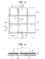
- Fig. 3 shows an image sensing element portion of a large area X-ray image sensing apparatus of a 414 mm square that is formed by tessellating nine image sensing elements 101A to 101I of a 138 mm square.
- Fig. 4 shows a 4-4 cross section of Fig. 3 .
- a scintillator plate 201 consisting of a scintillator such as Gd 2 O 2 S or CsI using europium, terbium or the like as an inert body is arranged on an FOP (fiber optic plate) 202.
- FOP fiber optic plate
- X-ray 202 is irradiated on the scintillator and converted to visible light. This visible light is detected by the image sensing elements 101A to 101I.
- the scintillator is preferably selected such that its light emitting wave length conforms to the sensitivity of the image sensing elements 101A to 101I.
- Reference numeral 204 denotes an external processing substrate having a circuit that supplies power, clocks or the like for the image sensing elements 101A to 101I and takes out signals from the image sensing elements to process them.
- Reference numeral 205 denotes TABs (Tape Automated Bonding) for electrically connecting each of the image sensing elements 101A to 101I and the external processing substrate.
- Clocks, power or the like of the image sensing elements 101A to 101I are inputted by and a signal from a pixel is outputted to the external processing substrate 204 arranged in the back side of the image sensing elements 101A to 101I, through the TABs 205 connected to electrode pads provided at an end of the image sensing element.
- Fig. 5 shows the case in which one image sensing element is taken out from an eight-inch wafer 300, which is currently a mainstream wafer.
- the eight-inch wafer 300 is an N-type wafer.
- Each of the CMOS type image sensing elements 101A to 1011 of 138 mm square is created using this eight-inch wafer 300 by a CMOS process.
- Fig. 6 illustrates a configuration of a pixel part forming each pixel of the CMOS type image sensing elements 101A to 101I.
- Reference numeral 401 denotes a photodiode for performing photoelectric conversion (photoelectric conversion section)
- 402 denotes a floating diffusion for accumulating charges
- 403 denotes a transfer MOS transistor (transfer switch) for transferring charges generated by the photodiode 401 to the floating diffusion 402
- 404 denotes a reset MOS transistor (reset switch) for discharging the charges accumulated in the floating diffusion 402
- 405 denotes a row selecting MOS transistor (row selection switch) for selecting a row
- 406 denotes an amplification MOS transistor (pixel amplifier) that functions as a source follower.
- Fig. 7 shows a schematic view of an entire circuit with 3 x 3 pixels.
- a gate of the transfer switch 403 is connected to a ⁇ TX 502 coming from a vertical shift register being a type of a vertical scanning circuit
- a gate of the reset switch 404 is connected to a ⁇ RES 503 coming from the vertical scanning circuit 501
- a gate of the row selection switch 405 is connected to a ⁇ SEL 504 coming from the vertical scanning circuit 501.
- Photoelectric conversion is performed in the photodiode 401.
- the transfer switch 403 is in the off state and the charges photoelectrically converted in this photodiode are not transferred to the gate of the source follower 406 forming a pixel amplifier.
- the gate of the source follower 406 forming the pixel amplifier is turned on by the reset switch 404 before starting the accumulation and initialized to an appropriate voltage. This generates a reference signal containing a noise component.
- a source follower circuit composed of a load current source and the pixel amplifier 406 enters an operation state, and a charge at the time of reset is transferred to the gate of the sour follower 406 forming the pixel amplifier, by turning on transfer switch 403, whereby this noise signal becomes readable. Then, a noise signal output of a row selected by the row selecting MOS 405 is generated on a vertical output line (signal output line) 505 and accumulated in a not-shown storage element which is not shown.
- the reset switch 404 is turned off and the row selection switch 405 is turned on next, the source follower circuit composed of the load current source and the pixel amplifier 406 enters an operation state.
- a noise signal is included mixedly in an accumulation signal of this photodiode.
- the noise signal is subtracted from the accumulation signal in a subtraction circuit (not shown) inside an image sensing element, to thereby obtain an image sensing signal.
- This output is sequentially read out to an output section 508 via the horizontal output line by driving a row selection switch (multiplexer) 506 using a horizontal shift register 507 that is a type of a horizontal scanning circuit.
- Fig. 8 shows an example of a unit block (a unit for selecting and driving one row) 601 of the vertical shift register 501, which is arranged on a substrate of an image sensing element.
- the unit block 601 of the vertical shift register 501 is arranged with a one-pixel circuit 602 in a one-pixel area (one cell) in Fig. 8 .
- the one-pixel circuit 602 is as shown in Fig. 4 .
- the vertical shift register is shown as a simple circuit that is composed of a static shift register 604 and a transfer gate 605 in order to produce a transfer signal ⁇ TX, a reset signal ⁇ RES, a row selection signal ⁇ SEL. These are driven by a signal from a clock signal line (not shown).
- a circuit configuration of a shift register is not limited to this, and an arbitrary circuit configuration can be adopted according to various methods of driving such as pixel addition or read-out with pixel.
- an n to 2 n decoder can be used rather than a shift register. Sequential scanning becomes possible as in a shift register by connecting a counter output that sequentially increments, to an input of the decoder.
- an image of arbitrary plural-pixel areas by random scanning can be obtained by inputting an address of a plural-pixel area where an image is desired to be formed, into the input of the decoder.
- Fig. 9 shows an enlarged view of a position denoted by reference numeral 10 in Fig. 3 of the image sensing apparatus according to the first embodiment.
- an image sensing element 101A and an image sensing element 101B are arranged adjacent to each other.
- the image sensing elements 101A and 101B are formed of a plurality of photoelectric converting elements, and each photoelectric converting element has a photoelectric conversion section.
- a gap 103 is inevitably generated.
- centroids 106 of photoelectric conversion sections 105 of (inside) photoelectric converting elements not contacting the gap 103 and centroids 107 of the photoelectric conversion sections 104 of photoelectric converting elements contacting the gap 103 are arranged at equal intervals over the image sensing elements 101A and 101B. In this way, distortion of an image can be prevented at a border of the image sensing element 101A and the image sensing element 101B.
- a one-pixel signal is obtained by collecting signals obtained from the plurality of photoelectric converting elements
- distortion of an image is also prevented by performing voltage addition. That is, as shown in Fig. 9 , if a pixel signal for a plural-pixel area 108 is obtained by adding voltages generated in photoelectric conversion sections of four photoelectric converting elements in the plural-pixel area 108, a position of a one-pixel signal for the plural-pixel area 108 is a position denoted by reference numeral 110 (a position coinciding with an average position of centroids of the photoelectric conversion section of the four photoelectric converting elements in the plural-pixel area 108).
- a position of the one-pixel signal for the plural-pixel area 109 is a position denoted by reference numeral 112 (a position coinciding with an average position of centroids of the photoelectric conversion sections of the four photoelectric converting elements in the plural-pixel area 109). Therefore, the pixel centroids 110 and 112 are arranged at equal intervals.
- Fig. 10 shows an example of a circuit configuration when voltages in four pixels are added.
- the voltages of the four pixels may be added after reading a voltage generated in each pixel from an amplifier 508.
- the voltages of the four pixels can be added simply by providing latches and adders for three pixels as shown in Fig. 11 .
- the central latch among the latches for three pixels function as a (one row - one pixel) memory.
- the voltages may be read in accordance with a reading address of a predetermined order and then digitally added after A/D converting an output of the amplifier 508 and writing it in a memory in accordance with a predetermined writing address. Procedures after the A/D conversion can be performed also by an information-processing apparatus such as a personal computer.
- a basic configuration of a second embodiment is the same as that of the first embodiment.
- Fig. 12 shows an enlarged view of the position denoted by reference numeral 10 in Fig. 3 of an image sensing apparatus according to this embodiment.
- plural-pixel areas for adding pixel signals are made as denoted by reference numerals 208 and 209.
- a position of a one-pixel signal for the plural-image area 208 is a position denoted by reference numeral 210 (a position coinciding with an average position of centroids of photoelectric conversion sections of four photoelectric converting elements in the plural-pixel area 208) both in the cases of charge addition and voltage addition.
- a position of a one-pixel signal for the plural-pixel area 209 is a position denoted by reference numeral 211 (a position coinciding with an average position of centroids of photoelectric conversion sections of four photoelectric converting elements in the plural-pixel area 209) both in the cases of charge addition and voltage addition.
- Fig. 13 shows a view of a circuit configuration for adding charges generated in four pixels.
- this circuit configuration after transferring charges accumulated in a photodiode to a floating diffusion by turning on a transfer switch, the charges are averaged among the four pixels by turning on switches 701, 702 and 703, and thereafter a row selection switch is turned on.
- pixel centroids 210 and 211 for each plural-pixel area are arranged at equal intervals regardless of whether pixel signals are added by the charge addition or are added by the voltage addition.
- a basic configuration of a third embodiment is the same as that of the first embodiment.
- Fig. 14 shows an enlarged view of the position denoted by reference numeral 10 in Fig. 3 of the image sensing apparatus according to this embodiment.
- the width of the photoelectric conversion sections 301 is made equal to the width of the photoelectric conversion sections 104, whereby the area of the photoelectric conversion sections 104 and the area of the photoelectric conversion sections 301 are made equal in this example.
- the area of the photoelectric conversion sections 104 and the area of the photoelectric conversion sections 301 may be made equal by adjusting a relative height of the photoelectric conversion sections 301 with respect to the height of the photoelectric conversion sections 104 or by adjusting a relative width and height of the photoelectric conversion sections 301 with respect to the width and the height of the photoelectric conversion sections 104. That is, as long as the area of the photoelectric conversion sections 301 is made equal to the area of the photoelectric conversion sections 104, an adjusting part of dimensions does not matter.
- the positions of the photoelectric conversion sections 104 and the positions of the photoelectric conversion section 301 are adjusted such that centroid positions 107 of the photoelectric conversion sections 104, centroid positions 302 of the photoelectric conversion sections 301 and centroid positions 106 of the photoelectric conversion sections 105 are arranged at equal intervals.
- the positions and the size of the photoelectric conversion sections 104 and the positions and the size of the photoelectric conversion sections 301 are adjusted such that the centroid positions 106, 107 and 302 are arranged at equal intervals and the area of the photoelectric conversion sections 104 and the area of the photoelectric conversion sections 301 are made equal.
- the plural-pixel area 303 is a plural-pixel area consisting of two photoelectric converting elements adjacent to the gap 103 and two photoelectric converting elements adjacent to the two photoelectric converting elements that are adjacent to the gap.
- a fourth embodiment is a configuration in which scanning circuits 304 are arranged between the photoelectric conversion sections 301 and the photoelectric conversion sections 104 in the configuration of the third embodiment as shown in Fig. -16.
- the scanning circuit 304 is a vertical scanning circuit in the plural-pixel area 10 ( Fig. 3 ), it is a horizontal scanning circuit in the plural-pixel area 11 ( Fig. 3 ).
- scanning circuits are arranged in spaces between the narrowed photoelectric conversion sections 301 and photoelectric conversion sections 104, whereby the scanning circuits can be arranged in the image sensing element without breaking the condition that the pixel centroids are arranged at equal intervals, irrespective of whether a one-pixel signal is obtained from each photoelectric converting element or one-pixel signals are obtained from a plurality of photoelectric elements.
- a fifth embodiment is a configuration in which scanning circuits 304 are arranged between the photoelectric conversion sections 301 and the photoelectric conversion sections 104 in the configuration of the third embodiment as shown in Fig. 17 .
- the scanning circuit 304 is a vertical scanning circuit in the plural-pixel area 10 ( Fig. 3 ), it is a horizontal scanning circuit in the plural-pixel area 11 ( Fig. 3 ).
- scanning circuits are arranged in spaces between the narrowed photoelectric conversion sections 301 and photoelectric conversion sections 104, whereby the scanning circuits can be arranged in the image sensing element without breaking the condition that the pixel centroids are arranged at equal intervals, irrespective of whether a pixel signal is obtained from each photoelectric converting element or one-pixel signals are obtained from a plurality of photoelectric elements.
- pixels 104 opposing adjacent to each other are added in the gap between the image sensing elements 101A and 101B, whereby the distance between added pixel centroids 113 and the one-pixel centroid 302 of the other photoelectric converting element and the distance between the one-pixel centroids 302 and 106 can be made to coincide with each other.
- a basic configuration of the fifth embodiment is as described below.
- Fig. 16 shows an enlarged view of the position denoted by reference numeral 10 in Fig. 3 of the image sensing apparatus according to this embodiment.
- the positions of the photoelectric conversion sections 104 and the positions of the photoelectric conversion section 301 are adjusted such that added centroid positions 107 of the photoelectric conversion sections 104, centroid positions 302 of the photoelectric conversion sections 301 and centroid positions 106 of the photoelectric conversion sections 105 are arranged at equal intervals.
- the positions and the size of the photoelectric conversion sections 104 and the positions and the size of the photoelectric conversion sections 301 are adjusted such that the added centroid positions 113 of the pixels opposing each other through the gap, the centroids 302 of the adjacent photoelectric converting elements and the centroids 106 of the other photoelectric converting elements are arranged at equal intervals.
- the position 113 of the one-pixel signal for the plural-pixel area 305 and the centroid positions 302 and 106 for the one-pixels 301 and 105, respectively, are arranged at equal intervals both in the cases of the charge addition and the voltage addition, whereby distortion of an image is eliminated.
- signals of a plurality of photoelectric conversion sections of a plural-pixel area are added, influence of offset for each image sensing element is also reduced.
- processing is performed such-that a one-pixel signal is obtained by adding signals of a plurality of photoelectric conversion sections within a plural-pixel area, a one-pixel signal is obtained from each photoelectric conversion section in the other areas, and an image is obtained by an image processing circuit (not shown) using the one-pixel signal obtained by addition and the one-pixel signal from each photoelectric section.
- the examples of adding signals in the state of analog signals are shown as an adding circuit.
- signals may be added after being converted to digital signals by an analog/digital converting circuit.
- pixel signals arranged at equal intervals can be obtained in a border between image sensing elements not only in the case in which a one-pixel signal is obtained from each photoelectric converting element but also in the case in which one-pixel signals are obtained from a plurality of photoelectric converting elements in an image sensing apparatus that is configured by tessellating a plurality of image sensing elements.
- an image obtained from the image sensing apparatus is never distorted even in borders between the image sensing elements.
- the photoelectric conversion sections other than those 104, 105 and 301 are light-shielded with a light shielding member (not shown) which is formed with a metal layer such as aluminum layer or the like.
- a photoelectric conversion section corresponds to an opening portion of the light shielding member.
- an addition circuit, a transfer switch, a reset switch, a pixel amplifier and the like other than the photoelectric conversion section (a photodiode) are arranged under a light shielding member, thereby being shielded from light.
- the scanning circuit 304 and common processing circuit shown in Figs. 16 and 17 are also arranged under a light shielding member, thereby being shielded from light.
- the applicant has proposed an image sensing apparatus having an image sensing element as shown in Fig. 18 for the purpose of providing a seamless image using a high-performance image sensing element of a plurality of monocrystal silicon.
- reference numeral 2101 denotes a photoelectric conversion section (photodiode) of each of a plurality of photoelectric converting elements provided in an image sensing element
- 2102 denotes a vertical shift register that is a type of a vertical scanning circuit
- 2103 denotes a horizontal shift register that is a type of a horizontal scanning circuit
- 2104 denotes a switch forming a multiplexer for alternately supplying a signal read out on a vertical reading line to a horizontal reading line
- 2105 denotes an external terminal (having a bump 2106) for supplying power and signal from the outside or supplying a signal to the outside
- 2107 denotes a protective circuit for protecting an image sensing element from a high voltage and a high current from the outside.
- centroids of the photoelectric conversion sections shown by "x" are not arranged at equal intervals. This is because the centroids of the photoelectric conversion sections, the left sides of which are eroded by the vertical shift register 2102, are moved to the right, centroids of the photoelectric conversion sections, the lower sides of which are eroded by the switch 2104, are moved upward, and centroids of the photoelectric conversion section, the upper side of which are eroded by the protective circuit 2107, are moved downward.
- an image sensing apparatus in which centroids of photoelectric conversion sections are arranged at equal intervals even if a scanning circuit is arranged in an image sensing area that is an effective pixel area of an image sensing element, will be described in the following embodiments.
- Fig. 19 shows a situation in which the unit block (unit for selecting and driving one row) 601 of the vertical shift register 501 is arranged inside a photoelectric conversion section 602 of a one-pixel area (one cell).
- the vertical shift register is structured as a circuit that is composed of the static-type shift register 604 and the transfer gate 605 in order to produce a transfer signal ⁇ TX, a reset signal ⁇ RES and a row selection signal ⁇ SEL. These are driven by a signal from a clock signal line (not shown).
- a circuit configuration of a shift register is not limited to this, and an arbitrary circuit configuration may be adopted according to various methods of driving such as pixel addition and read-out with thinning out.
- a common processing circuit means a circuit such as a final signal output amplifier, a serial/parallel converting multiplexer, an amplifier or various gate circuits, which collectively processes a plurality of pixels in common.
- the common processing circuit is functionally a circuit for outputting an image signal of each pixel read out on a vertical reading line to the outside through a horizontal reading line and an amplifier.
- an individual circuit means a circuit such as a photodiode, a transfer switch, a pixel selection switch or a pixel output amplification circuit, which processes one pixel only
- Fig. 20 shows a configuration (plan view) of an image sensing element of the sixth embodiment.
- a vertical shift register 501B, a horizontal shift register 507B and a common processing circuit are arranged in an effective pixel area of the image sensing element.
- Reference numeral 601A denotes circuits for one row among vertical scanning circuits
- 601B denotes circuits (unit blocks) for one column among horizontal scanning circuits
- 601C denotes circuits (unit blocks) for one column among common processing circuits.
- the centroid of the photoelectric section 602 in which the circuit 601A is arranged in the center is identical with the centroid of the photoelectric conversion section 602 in which the circuit 601A is not arranged.
- the centroid of the photoelectric conversion section 602 in which the circuit 601B is arranged in the center is identical with the centroid of the photoelectric conversion section 602 in which the circuit 601B is not arranged.
- centroid of the photoelectric conversion section 602 in which the circuit 601C is arranged in the center is identical with the centroid of the photoelectric conversion section 602 in which the circuit 601C is not arranged.
- centroid of the photoelectric conversion section 602 in which the circuit 601A and the circuit 601B are arranged symmetrically with respect to the central line of the photoelectric conversion section 602 is identical with centroid of the photoelectric conversion section 602 in which the circuit 601A and the circuit 601B are not arranged.
- centroid of the photoelectric conversion section 602 in which the circuit 601A and the circuit 601C are arranged symmetrically with respect to the central line of the photoelectric conversion section 602 is identical with centroid of the photoelectric conversion section 602 in which the circuit 601A and the circuit 601C are not arranged.
- the centroids of the photoelectric conversion sections 602 are arranged at equal intervals. Therefore, the centroids of the photoelectric conversion sections 602 are arranged at equal intervals even if the circuits 601A, 601B and 601C are arranged.
- a static-type shift register is used as a shift register being an example of a scanning circuit.
- Various circuit configurations can be applied to the shift register by designing. In this embodiment, a general example of a circuit is described. What is important is the point that the static shift register is used.
- an error there is an error similar to an error (soft error) due to an action of a hot electron known as a failure in an MOS type dynamic RAM.
- a shift register used for driving pixels of an image sensing element will now be described.
- a shift register circuit is used for sequentially transferring pulse signals.
- Figs. 21 and 22 show-examples of a configuration of a static shift register circuit.
- This shift register circuit is disclosed in Japanese Patent Application Laid-open No. 9-223948 .
- a first stage section of the shift register circuit consists of one inverter and two clocked inverters in the configuration of Fig. 21 and consists of three inverters and two CMOS transfer gates in the configuration of Fig. 22 .
- clock signals CLK and /CLK (“/" indicates a negative logic) having opposite phases are inputted in each of the two clocked inverters or each of the two CMOS transfer gates.
- clock signals having opposite phases are inputted in each of adjacent shift register circuits.
- Fig. 23 shows a view of an internal configuration of an inverter.
- Fig. 24 shows a view of an internal configuration of a clocked inverter.
- the clocked inverter is composed of a p channel type input transistor Tr1, a p channel type clocked transistor Tr2, an n channel type clocked transistor Tr3 and an n channel type input transistor Tr4, which are serially connected between a power supply and a ground. An output is taken out from a connecting point of the transistor Tr2 and the transistor Tr3.
- the shift register circuit used in a driving circuit is usually driven in synchronous with a clock by two clock signals having opposite phases.
- Fig. 25 shows an example of a configuration of a dynamic-type shift register circuit.
- a clocked inverter or a transfer gate and an inverter for feedback is provided in the static-type shift register
- a transistor TR in which clocks are applied by a gate, and a capacitor C are provided between inverters in the dynamic-type shift register, whereby the number of elements is reduced to realize low power consumption.
- This shift circuit is disclosed in Japanese Patent Application Laid-open No. 5-218814 .
- the dynamic-type shift register theoretically performs operations for accumulating charges in the capacitor to hold data.
- the dynamic-type shift register In the dynamic-type shift register, if leakage exists in an interface between a pn junction surface or an insulating layer and silicon, the capacitor cannot hold charges and the dynamic-type shift register does not operate normally.
- the dynamic-type shift register When the dynamic-type shift register is used in a place where X-ray is irradiated, it is susceptible to damages by the X-ray and does not operate due to increase of a leak current, whereby a problem concerning reliability arises. In addition, a normal image cannot be obtained because of a failure due to a hot electron caused by X-ray.
- the static-type shift register is relatively insusceptible to an influence of X-ray, thus it can be used in a place where X-ray is directly irradiated as in this embodiments Therefore, if the static-type shift register is used, an image sensing apparatus with fewer damages or errors caused by X-ray and improved reliability can be realized.
- an n to 2 n decoder can be used rather than a shift register. Sequential scanning becomes possible as in a shift register by connecting a counter output that sequentially increments, to an input of the decoder.
- an image of an arbitrary area by random scanning can be obtained by inputting an address of an area where an image is desired to be formed, into the input of the decoder.
- This embodiment uses a CMOS sensor as an image sensing element, it is preferred in forming a large image sensing apparatus that consumes less power.
- a signal is taken out to the outside from an image sensing element through an electrode pad, around which there is a large floating capacity. Therefore, a transmission property of a signal can be compensated by providing the amplifier 508 in the front stage of the electrode pad.
- An image sensing apparatus of the seventh embodiment is the same as the sixth embodiment in a basic configuration and is different from the sixth embodiment in a format of arranging a scanning circuit and a common processing circuit.
- Fig. 26 shows a configuration (plan view) of an image sensing element of this embodiment.
- Reference numeral 601D denotes circuits for one row of vertical scanning circuits
- 601E denotes circuits for one column of horizontal scanning circuits
- 601F denotes circiuts for one column of common processing circuits.
- the centroid of the photoelectric section 602 in which the circuits 601D are arranged in the four corners is identical with the centroid of the photoelectric conversion section 602 in which the circuits 601D are not arranged.
- the centroid of the photoelectric conversion section 602 in which the circuits 601E are arranged in the four corners is identical with the centroid of the photoelectric conversion section 602 in which the circuits 601E are not arranged.
- centroid of the photoelectric conversion section 602 in which the circuits 601F are arranged in the four corners is identical with the centroid of the photoelectric conversion section 602 in which the circuits 601F are not arranged. Moreover, the centroid of the photoelectric conversion section 602 in which the circuits 601D and the circuits 601E are arranged in the four corners of the photoelectric conversion section 602 is identical with the centroid of the photoelectric conversion section 602 in which the circuits 601D and the circuits 601E are not arranged.
- centroid of the photoelectric conversion section 602 in which the circuits 601D and the circuits 601F are arranged in the four corners of the photoelectric conversion section 602 is identical with centroid of the photoelectric conversion section 602 in which the circuits 601D and the circuits 601F are not arranged.
- the centroids of the photoelectric conversion sections 602 are arranged at equal intervals. Therefore, the centroids of the photoelectric conversion sections 602 are arranged at equal intervals even if the circuits 601D, 601E and 601F are arranged.
- An image sensing apparatus of the eighth embodiment is the same as the sixth embodiment in a basic configuration and is different from the sixth embodiment in a format of arranging a scanning circuit and a common processing circuit.
- Fig. 27 shows a configuration (plan view) of an image sensing element of this embodiment.
- Reference numeral 501B denotes a vertical scanning circuit
- 507B denotes a horizontal scanning circuit
- 509 denotes a common processing circuit.
- the centroid of the photoelectric section 602 in which the vertical scanning circuit 501B is arranged in the center is identical with the centroid of the photoelectric conversion section 602 in which the vertical scanning circuit 501B is not arranged.
- the centroid of the photoelectric conversion section 602 in which the horizontal scanning circuit 507B is arranged in the center is identical with the centroid of the photoelectric conversion section 602 in which the horizontal scanning circuit 507B is not arranged.
- centroid of the photoelectric conversion section 602 in which the common processing circuit 509 is arranged in the center is identical with the centroid of the photoelectric conversion section 602 in which the common processing circuit 509 is not arranged. Moreover, the centroid of the photoelectric conversion section 602 in which the vertical scanning circuit 501B and the horizontal scanning circuit 507B are arranged in the center is identical with centroid of the photoelectric conversion section 602 in which the vertical scanning circuit 501B and the horizontal scanning circuit 507B are not arranged.
- centroid of the photoelectric conversion section 602 in which the vertical scanning circuit 501B and the common processing circuit 509 are arranged in the center is identical with centroid of the photoelectric conversion section 602 in which the vertical scanning circuit 501B and the common processing circuit 509 are not arranged.
- the centroids of the photoelectric conversion sections 602 are arranged at equal intervals. Therefore, the centroids of the photoelectric conversion sections 602 are arranged at equal intervals even if the vertical scanning circuit 501B, the horizontal scanning circuit 507B and the common processing circuit 509 are arranged.
- a power supply line can be arranged on the scanning circuits and/or the common processing circuits for shielding X-ray.
- a material of the power supply line copper or the like, which has high absorptance is used.
- Scanning circuits and common processing circuits are arranged inside a photoelectric conversion section such that the centroid of the photoelectric conversion section does not move in the sixth to the eighth embodiments.
- a light shielding section is arranged in such manner that it covers a part of a photoelectric conversion section, and the light shielding section is arranged inside the photoelectric conversion section such that the centroid of the photoelectric conversion section does not move.
- scanning circuits and common processing circuits are provided below the light shielding section.
- the light shielding section consists of, for example, a metal for wiring.
- Fig. 28 shows a configuration (plan view) of an image sensing apparatus of the ninth embodiment.
- Reference numeral 611A denotes a light shielding section for covering circuits for one row of vertical scanning circuits
- 611B denotes a light shielding section for covering circuits for one column of horizontal scanning circuits
- 611C denotes a light shielding section for covering circuits for one column of common processing circuits
- reference numeral 611D denotes a light shielding section for covering circuits for one row of the vertical scanning circuits and circuits for one column of the horizontal scanning circuits
- 611E denotes a light shielding section for covering circuits for one row of the vertical scanning circuits and circuits for one column of the common processing circuits.
- the centroid of the photoelectric conversion section 602 in which the light shielding section 611A is arranged in the center is identical with the centroid of the photoelectric conversion section 602 in which the light shielding section 611A is not arranged.
- the centroids of the photoelectric conversion sections 602 in which the light shielding sections 611B, 611C, 611D and 611E are arranged in the center are identical with the centroids of the photoelectric conversion section 602 in which the light shielding sections 611B, 611C, 611D and 611E are not arranged.
- the centroids of the photoelectric sections 602 are arranged at equal intervals. Therefore, even if the light shielding sections 611A to 611E are arranged, the centroids of the photoelectric conversion sections 602 are arranged at equal intervals.
- a light shielding section is arranged only in a photoelectric conversion section in which scanning circuits and/or common processing circuits are arranged.
- a light shielding section is arranged either in a photoelectric conversion section in which scanning circuits and/or common processing circuits are arranged or in a photoelectric conversion section in which scanning circuits and common processing circuits are not arranged. That is, the light shielding section is arranged in any photoelectric conversion section.
- Fig. 29 shows a configuration (plan view) of an image sensing element of this embodiment.
- Reference numeral 611F denotes light shielding sections, which are arranged in all photoelectric conversion sections. Parts of the light shielding sections (e.g., the light shielding section which is in the position of the light shielding section 611A) cover circuits for one row of vertical scanning circuits. In addition, another part of the light shielding sections (e.g., the light shielding section which is in the position of the light shielding section 611B) cover circuits for one column of horizontal scanning circuits. Moreover, another part of the light shielding sections (e.g., the light shielding section which is in the position of the light shielding section 611C) cover circuits for one column of common processing circuits.
- the light shielding sections cover circuits for one row of the vertical scanning circuit and circuits for one column of the horizontal scanning circuits.
- another part of the light shielding sections cover circuits for one row of the vertical scanning circuits and circuits for one column of the common processing circuits.
- the centroid of the photoelectric conversion section 602 in which the light shielding section 611F is arranged in the center is identical with the centroid of the photoelectric conversion section 602 in which the light shielding section 611A is not arranged.
- the centroids of the photoelectric conversion section 602 are arranged at equal intervals. Therefore, even if the light shielding sections 611F are arranged, the centroids of the photoelectric conversion section 602 are arranged at equal intervals.
- the light shielding section 611F is arranged in the center of the photoelectric conversion section 602 such that the centroid of the photoelectric conversion section 602 does not move.
- Fig. 30 shows a configuration (plan view) of an image sensing element of an eleventh embodiment.
- Reference numeral 611G denotes light shielding sections, which are arranged in all photoelectric conversion sections. Parts of the light shielding sections (e.g., the light shielding section which is in the position of the light shielding section 611A) cover circuits for one row of vertical scanning circuits. In addition, another part of the light shielding sections (e.g., the light shielding section which is in the position of the light shielding section 611B) cover circuits for one column of horizontal scanning circuits. Moreover, another part of the light shielding sections (e.g., the light shielding section which is in the position of the light shielding section 611C) cover circuits for one column of common processing circuits.
- light shielding sections cover circuits for one row of the vertical scanning circuits and circuits for one column of the horizontal scanning circuits.
- another part of the light shielding sections cover circuits for one row of the vertical scanning circuits and circuits for one column of the common processing circuits.
- the light shielding section 611G is arranged such that the centroid of the photoelectric conversion section 602 moves.
- the centroids of the photoelectric conversion sections 602 are arranged at equal intervals even if the light shielding sections 611G are provided.
- a light shielding section is arranged inside a photoelectric conversion section for each pixel in the effective pixel area, and scanning circuits and common processing circuits are arranged below it.
- image sensing elements can be arranged such that a substantial gap is not generated between the image sensing elements, discontinuity or lack of an image does not occur between the image sensing elements even if an entire circumference of a given image sensing element is surrounded by other image sensing elements to configure an image sensing apparatus which forms one image by five (in the case of a crucifix-shaped area) or nine (in the case of a rectangular area of 3/row x 3/column) or more image sensing elements.
- Fig. 31 shows a twelfth embodiment that is an example of an application of the image sensing apparatus of the first to the eleventh embodiments to an X-ray diagnosis system.
- X-ray 6060 generated by an X-ray tube 6050 penetrates a chest 6062 of a patient or an object 6061 and is incident on a radiation image sensing apparatus 6040 provided with the scintillator 201, the FOP 202, the image sensing element 101 and the external processing substrate 204.
- the incident X-ray includes information of the inside of the body of the patient 6061.
- the scintillator emits light in response to the incidence of the X-ray, the light is photoelectrically converted by the image sensing element, and electric information is obtained. This information is digitally converted, subject to image processing by an image processor 6070 and observed on a display 6080 in a control room.
- this information can be transferred to a distant place by transferring means such as telephone lines 6090, can be indicated on a display 6081 or saved in saving means such as an optical disk in a doctor's room in another place, and enables a doctor in the distant place to make a diagnosis.
- the information can be recorded in a film 6110 by a film processor 6100.
- An image sensing apparatus comprising:
- Subject-matter 2 An image sensing apparatus according to subject-matter 1, wherein the centroids of said photoelectric conversion sections are arranged at equal intervals in the area extending over said plurality of image sensing elements.
- Subject-matter 3 An image sensing apparatus according to subject-matter 1, wherein said adding circuit includes a voltage adding circuit adapted to add the signals generated in said plurality of photoelectric conversion sections at a voltage level.
- Subject-matter 4 An image sensing apparatus according to subject-matter 3, wherein said voltage adding circuit is arranged so as to add signals generated in photoelectric conversion sections of one image sensing element.
- Subject-matter 5 An image sensing apparatus according to subject-matter 3, wherein said voltage adding circuit is arranged so as to add signals generated in photoelectric conversion sections in a plurality of image sensing elements.
- Subject-matter 6 An image sensing apparatus according to subject-matter 1, wherein said adding circuit includes a charge adding circuit adapted to add charge levels of the signals generated in said plurality of photoelectric conversion sections.
- Subject-matter 7 An image sensing apparatus according to subject-matter 6, wherein said charge adding circuit adds signals generated in photoelectric conversion sections of one image sensing element.
- An image sensing apparatus comprising:
- Subject-matter 9 An image sensing apparatus according to subject-matter 8, wherein the centroids of said photoelectric conversion sections are arranged at equal intervals in the area extending over said plurality of image sensing elements.
- Subject-matter 10 An image sensing apparatus according to subject-matter 8, wherein said adding circuit includes a voltage adding circuit adapted to add charge levels of the signals generated in said plurality of photoelectric conversion sections.
- Subject-matter 11 An image sensing apparatus according to subject-matter 10, wherein said voltage adding circuit is arranged so as to add signals generated in photoelectric conversion sections of one image sensing element.
- Subject-matter 12 An image sensing element according to subject-matter 10, wherein said voltage adding circuit is arranged so as to add signals generated in photoelectric conversion sections in a plurality of image sensing elements.
- Subject-matter 13 An image sensing apparatus according to subject-matter 8, wherein said adding circuit includes a charge adding circuit adapted to add charge levels of the signals generated in said plurality of photoelectric conversion sections.
- Subject-matter 14 An image sensing apparatus according to subject-matter 13, wherein said charge adding circuit adds signals generated in photoelectric conversion sections of one image sensing element.
- An image sensing apparatus comprising:
- An image sensing apparatus comprising:
- An image sensing apparatus comprising:
- Subject-matter 18 An image sensing apparatus according to subject-matter 17, wherein the first one-pixel signal and the second one-pixel signal are arranged at equal intervals in an area extending over said plurality of image sensing areas.
- An image sensing apparatus comprising:
- Subject-matter 20 An image sensing apparatus according to subject-matter 1, further comprising:
- Subject-matter 21 An image sensing apparatus according to subject-matter 8, further comprising:
- Subject-matter 22 An image sensing apparatus according to subject-matter 17, further comprising:
- Subject-matter 23 An image sensing apparatus according to subject-matter 19, further comprising:
- Subject-matter 24 An image sensing apparatus comprising a plurality of image sensing areas adapted to sense an object image, wherein said object image is sensed over said plurality of image sensing areas and each image sensing area is provided with a plurality of photoelectric conversion sections, wherein scanning circuit is arranged inside part of said photoelectric conversion sections, and wherein centroids of said photoelectric conversion sections in which said scanning circuits are arranged and centroids of said photoelectric conversion sections in which said scanning circuits are not arranged are arranged at equal intervals.
- Subject-matter 25 An image sensing apparatus comprising a plurality of image sensing areas each including a plurality of photoelectric conversion sections, wherein an object image is sensed over said plurality of image sensing areas and each of said plurality of image sensing areas has a first area in which a scanning circuit is arranged between photoelectric conversion sections and a second area in which said scanning circuit is not arranged between said photoelectric conversion sections, and wherein centroids of said photoelectric conversion sections of said first area and centroids of said photoelectric conversion sections of said second area are arranged at equal intervals.
- Subject-matter 26 An image sensing apparatus according to subject-matter 24, wherein said scanning circuit is provided with a shift register.
- Subject-matter 27 An image sensing apparatus according to subject-matter 26, wherein said shift register is a static type.
- Subject-matter 28 An image sensing apparatus according to subject-matter 24, wherein said scanning circuit is provided with a decoder.
- Subject-matter 29 An image sensing apparatus according to subject-matter 24, wherein a power supply line is arranged on said scanning circuit.
- Subject-matter 30 An image sensing apparatus comprising a plurality of image sensing areas, wherein an object image is sensed over said plurality of image sensing areas and each image sensing area is provided with a plurality of photoelectric conversion sections, wherein a common processing circuit adapted to selectively output to the outside signals from a vertical output line to which signals from said plurality of photoelectric conversion sections in a vertical direction are read out, via a horizontal output line are arranged inside said photoelectric conversion sections wherein and centroids of said photoelectric conversion sections in which said common processing circuits are arranged and centroids of said photoelectric conversion section in which said common processing circuits are not arranged are arranged at equal intervals.
- An image sensing apparatus comprising a plurality of image sensing areas each including a plurality of photoelectric conversion sections, wherein an object image is sensed over said plurality of image sensing areas and each of said plurality of image sensing areas has a first area in which a common processing circuit adapted to selectively output to the outside signals from a vertical output line to which signals from said plurality of photoelectric conversion sections in said vertical direction are read out, via a horizontal output line is arranged between said photoelectric converting areas, and second area in which said common circuit is not arranged between said photoelectric conversion sections, and wherein centroids of said photoelectric conversion sections of said first area and centroids of said photoelectric conversion sections of said second area are arranged at equal intervals.
- Subject-matter 32 An image sensing apparatus according to subject-matter 30, wherein said common circuit is provided with a multiplexer.
- Subject-matter 33 An image sensing apparatus according to subject-matter 30, wherein said common processing circuit is provided with an amplifier adapted to amplify signals transferred to said horizontal output line.
- Subject-matter 34 An image sensing apparatus according to subject-matter 30, wherein a power supply line is arranged on said common processing circuit.
- Subject-matter 35 An image sensing apparatus comprising a plurality of image sensing areas, wherein an object image is sensed over said plurality of image sensing areas and each image sensing area is provided with a plurality of photoelectric conversion sections, wherein light shielding region is arranged inside part of said photoelectric conversion sections and wherein centroids of said photoelectric conversion sections in which said light shielding sections are arranged and centroids of said photoelectric conversion sections in which said light shielding sections are not arranged are arranged at equal intervals.
- Subject-matter 36 An image sensing apparatus according to subject-matter 35, wherein a scanning circuit is arranged under said light shielding region.
- Subject-matter 37 An image sensing apparatus according to subject-matter 36, wherein said scanning circuit is provided with a shift register.
- Subject-matter 38 An image sensing apparatus according to subject-matter 37, wherein said shift register is a static type.
- Subject-matter 39 An image sensing apparatus according to subject-matter 36, wherein said scanning circuit is provided with a decoder.
- Subject-matter 40 An image sensing apparatus according to subject-matter 35, wherein a common processing circuit adapted to selectively output to the outside signals from a vertical output line to which signals from said plurality of photoelectric conversion sections in a vertical direction are read out, via a horizontal output line is arranged under said light shielding region.
- Subject-matter 41 An image sensing apparatus according to subject-matter 35, wherein said common processing circuit is provided with a multiplexer.
- Subject-matter 42 An image sensing apparatus according to subject-matter 35, wherein said common processing circuit is provided with an amplifier adapted to amplify the signals transferred to said horizontal output line.
- Subject-matter 43 An image sensing apparatus comprising a plurality of image sensing areas, wherein an object image is sensed over said plurality of image sensing areas and each image sensing area is provided with a plurality of photoelectric conversion sections, wherein light shielding regions are arranged inside said plurality of photoelectric conversion sections, and wherein centroids of said photoelectric conversion sections in which said light shielding regions are arranged are arranged at equal intervals.
- Subject-matter 44 An image sensing apparatus according to subject-matter 43, wherein a scanning circuit is arranged under said light shielding regions.
- Subject-matter 45 An image sensing apparatus according to subject-matter 43, wherein said scanning circuit is provided with a shift register.
- Subject-matter 46 An image sensing apparatus according to subject-matter 45, wherein said shift register is a static type.
- Subject-matter 47 An image sensing apparatus according to subject-matter 44, wherein said scanning circuit is provided with a decoder.
- Subject-matter 48 An image sensing apparatus according to subject-matter 43, wherein a common processing circuit adapted to selectively output to the outside signals from a vertical output line to which signals from said plurality of photoelectric conversion sections in a vertical direction are read out, via a horizontal output line is arranged under said light shielding regions.
- Subject-matter 49 An image sensing apparatus according to subject-matter 48, wherein said common processing circuit is provided with a noise eliminating circuit.
- Subject-matter 50 An image sensing apparatus according to subject-matter 48, wherein said common processing circuit is provided with an A/D converter.
- Subject-matter 51 An image sensing apparatus according to subject-matter 48, wherein said common processing circuit is provided with a multiplexer.
- Subject-matter 52 An image sensing apparatus according to subject-matter 48, wherein said common processing circuit is provided with an amplifier adapted to amplify signals transferred to said horizontal output line.
- An image sensing apparatus comprising a plurality of image sensing areas each including a plurality of photoelectric conversion sections, wherein an object image is sensed over a plurality of image sensing areas and each of said plurality of image sensing areas has a first area in which a scanning circuit and/or a common processing circuit adapted to selectively output to the outside signals from a vertical output line to which signals from said plurality of photoelectric conversion sections in the vertical direction are read out, to a horizontal output line are arranged between said photoelectric conversion sections, and a second area in which said scanning circuit and said common circuit are not arranged between said photoelectric conversion sections, and wherein light shielding means is arranged such that centroids of said photoelectric conversion sections of said first area and centroids of said photoelectric conversion sections of said second area are arranged at equal intervals.
- Subject-matter 54 An image sensing apparatus according to subject-matter 25, further comprising:
- Subject-matter 55 An image sensing apparatus according to subject-matter 31, further comprising:
- Subject-matter 56 An image sensing apparatus according to subject-matter 35, further comprising:
- Subject-matter 57 An image sensing apparatus according to subject-matter 43, further comprising:
- Subject-matter 58 An image sensing apparatus according to subject-matter 53, further comprising:
Landscapes
- Engineering & Computer Science (AREA)
- Multimedia (AREA)
- Signal Processing (AREA)
- Solid State Image Pick-Up Elements (AREA)
- Transforming Light Signals Into Electric Signals (AREA)
Applications Claiming Priority (3)
| Application Number | Priority Date | Filing Date | Title |
|---|---|---|---|
| JP2000227333A JP3715873B2 (ja) | 2000-07-27 | 2000-07-27 | 撮像装置、放射線撮像装置及びそれを用いた放射線撮像システム |
| JP2000234829A JP2002051262A (ja) | 2000-08-02 | 2000-08-02 | 撮像装置、放射線撮像装置及びそれを用いた放射線撮像システム |
| EP01306425A EP1176808A3 (fr) | 2000-07-27 | 2001-07-26 | Dispositif de prise de vue |
Related Parent Applications (1)
| Application Number | Title | Priority Date | Filing Date |
|---|---|---|---|
| EP01306425.8 Division | 2001-07-26 |
Publications (2)
| Publication Number | Publication Date |
|---|---|
| EP2290952A2 true EP2290952A2 (fr) | 2011-03-02 |
| EP2290952A3 EP2290952A3 (fr) | 2011-08-17 |
Family
ID=26596828
Family Applications (2)
| Application Number | Title | Priority Date | Filing Date |
|---|---|---|---|
| EP01306425A Withdrawn EP1176808A3 (fr) | 2000-07-27 | 2001-07-26 | Dispositif de prise de vue |
| EP20100181875 Withdrawn EP2290952A3 (fr) | 2000-07-27 | 2001-07-26 | Dispositif de prise de vue |
Family Applications Before (1)
| Application Number | Title | Priority Date | Filing Date |
|---|---|---|---|
| EP01306425A Withdrawn EP1176808A3 (fr) | 2000-07-27 | 2001-07-26 | Dispositif de prise de vue |
Country Status (2)
| Country | Link |
|---|---|
| US (5) | US7071980B2 (fr) |
| EP (2) | EP1176808A3 (fr) |
Cited By (2)
| Publication number | Priority date | Publication date | Assignee | Title |
|---|---|---|---|---|
| US9357972B2 (en) | 2012-07-17 | 2016-06-07 | Cyber Medical Imaging, Inc. | Intraoral radiographic sensors with cables having increased user comfort and methods of using the same |
| TWI693832B (zh) * | 2015-01-30 | 2020-05-11 | 日商瑞薩電子股份有限公司 | 攝像元件 |
Families Citing this family (41)
| Publication number | Priority date | Publication date | Assignee | Title |
|---|---|---|---|---|
| US7071980B2 (en) | 2000-07-27 | 2006-07-04 | Canon Kabushiki Kaisha | Image sensing apparatus |
| JP3750502B2 (ja) * | 2000-08-03 | 2006-03-01 | ソニー株式会社 | 固体撮像装置およびカメラシステム |
| JP3667214B2 (ja) * | 2000-08-25 | 2005-07-06 | キヤノン株式会社 | 固体撮像装置およびその駆動方法 |
| JP2002330349A (ja) * | 2001-04-26 | 2002-11-15 | Fujitsu Ltd | Xyアドレス型固体撮像装置 |
| AU2002308651A1 (en) * | 2001-05-04 | 2002-11-18 | Leberl, Franz, W. | Digital camera for and method of obtaining overlapping images |
| US7138696B2 (en) | 2001-10-19 | 2006-11-21 | Canon Kabushiki Kaisha | Image pickup apparatus, radiation image pickup apparatus and radiation image pickup system |
| JP3992504B2 (ja) * | 2002-02-04 | 2007-10-17 | 富士通株式会社 | Cmosイメージセンサ |
| JP4240917B2 (ja) * | 2002-06-13 | 2009-03-18 | コニカミノルタホールディングス株式会社 | 走査回路 |
| US20040012689A1 (en) * | 2002-07-16 | 2004-01-22 | Fairchild Imaging | Charge coupled devices in tiled arrays |
| US20040012684A1 (en) * | 2002-07-16 | 2004-01-22 | Fairchild Imaging | Image reconstruction techniques for charge coupled devices |
| US20040012688A1 (en) * | 2002-07-16 | 2004-01-22 | Fairchild Imaging | Large area charge coupled device camera |
| US7408195B2 (en) * | 2003-09-04 | 2008-08-05 | Cypress Semiconductor Corporation (Belgium) Bvba | Semiconductor pixel arrays with reduced sensitivity to defects |
| JP2005130382A (ja) * | 2003-10-27 | 2005-05-19 | Matsushita Electric Ind Co Ltd | 固体撮像装置 |
| US7795577B2 (en) * | 2004-08-25 | 2010-09-14 | Richard Ian Olsen | Lens frame and optical focus assembly for imager module |
| US7916180B2 (en) * | 2004-08-25 | 2011-03-29 | Protarius Filo Ag, L.L.C. | Simultaneous multiple field of view digital cameras |
| US7564019B2 (en) * | 2005-08-25 | 2009-07-21 | Richard Ian Olsen | Large dynamic range cameras |
| US20060054782A1 (en) | 2004-08-25 | 2006-03-16 | Olsen Richard I | Apparatus for multiple camera devices and method of operating same |
| US8124929B2 (en) * | 2004-08-25 | 2012-02-28 | Protarius Filo Ag, L.L.C. | Imager module optical focus and assembly method |
| JP4306603B2 (ja) * | 2004-12-20 | 2009-08-05 | ソニー株式会社 | 固体撮像装置および固体撮像装置の駆動方法 |
| KR100680469B1 (ko) | 2005-01-31 | 2007-02-08 | 매그나칩 반도체 유한회사 | 인접한 화소들 사이의 센싱노드들이 공유된 씨모스 이미지센서 |
| JP4561439B2 (ja) * | 2005-03-30 | 2010-10-13 | 株式会社デンソー | 撮像装置 |
| US20070102622A1 (en) * | 2005-07-01 | 2007-05-10 | Olsen Richard I | Apparatus for multiple camera devices and method of operating same |
| US7214998B2 (en) * | 2005-07-26 | 2007-05-08 | United Microelectronics Corp. | Complementary metal oxide semiconductor image sensor layout structure |
| US7964835B2 (en) | 2005-08-25 | 2011-06-21 | Protarius Filo Ag, L.L.C. | Digital cameras with direct luminance and chrominance detection |
| US20070258006A1 (en) * | 2005-08-25 | 2007-11-08 | Olsen Richard I | Solid state camera optics frame and assembly |
| JP4194633B2 (ja) * | 2006-08-08 | 2008-12-10 | キヤノン株式会社 | 撮像装置及び撮像システム |
| US7760258B2 (en) * | 2007-03-07 | 2010-07-20 | Altasens, Inc. | Apparatus and method for stabilizing image sensor black level |
| US20080266444A1 (en) * | 2007-04-27 | 2008-10-30 | Micron Technology, Inc. | Method, apparatus, and system for continuous autofocusing |
| JP4582205B2 (ja) * | 2008-06-12 | 2010-11-17 | トヨタ自動車株式会社 | 電動車両 |
| US7777171B2 (en) * | 2008-08-26 | 2010-08-17 | Eastman Kodak Company | In-pixel summing of charge generated by two or more pixels having two reset transistors connected in series |
| US8913166B2 (en) * | 2009-01-21 | 2014-12-16 | Canon Kabushiki Kaisha | Solid-state imaging apparatus |
| CN101901818B (zh) * | 2009-05-26 | 2013-06-05 | 鸿富锦精密工业(深圳)有限公司 | 影像感测器、侦测物体运动方向的装置及方法 |
| US8723827B2 (en) | 2009-07-28 | 2014-05-13 | Cypress Semiconductor Corporation | Predictive touch surface scanning |
| JP2012034350A (ja) * | 2010-07-07 | 2012-02-16 | Canon Inc | 固体撮像装置及び撮像システム |
| JP5751766B2 (ja) | 2010-07-07 | 2015-07-22 | キヤノン株式会社 | 固体撮像装置および撮像システム |
| JP5671890B2 (ja) * | 2010-08-31 | 2015-02-18 | 株式会社ニコン | 撮像装置 |
| TWI424746B (zh) * | 2011-02-14 | 2014-01-21 | 財團法人工業技術研究院 | 影像感測器及其感測方法 |
| JP6063160B2 (ja) * | 2012-07-20 | 2017-01-18 | 株式会社堀場製作所 | 放射線検出器 |
| JP6988796B2 (ja) * | 2016-04-22 | 2022-01-05 | ソニーグループ株式会社 | X線検出装置 |
| JP7046698B2 (ja) * | 2018-04-24 | 2022-04-04 | 浜松ホトニクス株式会社 | 放射線検出器、放射線検出器の製造方法、及び画像処理方法 |
| CN109545810A (zh) * | 2018-11-20 | 2019-03-29 | 京东方科技集团股份有限公司 | 一种平板探测器及其制备方法 |
Citations (7)
| Publication number | Priority date | Publication date | Assignee | Title |
|---|---|---|---|---|
| US4323925A (en) | 1980-07-07 | 1982-04-06 | Avco Everett Research Laboratory, Inc. | Method and apparatus for arraying image sensor modules |
| JPH05218814A (ja) | 1992-01-31 | 1993-08-27 | Sony Corp | フリツプフロツプ回路 |
| US5315101A (en) | 1992-02-08 | 1994-05-24 | U.S. Philips Corporation | Method of manufacturing a large area active matrix array |
| JPH09223948A (ja) | 1996-02-15 | 1997-08-26 | Sharp Corp | シフトレジスタ回路および画像表示装置 |
| EP0954032A2 (fr) * | 1998-04-30 | 1999-11-03 | Canon Kabushiki Kaisha | Dispositif de prise d'image à l'état solide et système utilisant ce dispositif |
| US6005911A (en) | 1995-11-17 | 1999-12-21 | Trex Medical Corporation | Large area array, single exposure digital mammography |
| EP1176808A2 (fr) | 2000-07-27 | 2002-01-30 | Canon Kabushiki Kaisha | Dispositif de prise de vue |
Family Cites Families (34)
| Publication number | Priority date | Publication date | Assignee | Title |
|---|---|---|---|---|
| US4412236A (en) * | 1979-08-24 | 1983-10-25 | Hitachi, Ltd. | Color solid-state imager |
| JPS62112382A (ja) * | 1985-11-12 | 1987-05-23 | Toshiba Corp | 半導体受光装置 |
| US5464984A (en) * | 1985-12-11 | 1995-11-07 | General Imaging Corporation | X-ray imaging system and solid state detector therefor |
| JPH0815322B2 (ja) * | 1986-05-21 | 1996-02-14 | キヤノン株式会社 | 固体撮像装置 |
| JP2735223B2 (ja) * | 1988-06-08 | 1998-04-02 | 日本放送協会 | 固体撮像装置 |
| JP2710292B2 (ja) * | 1991-06-12 | 1998-02-10 | シャープ株式会社 | 固体撮像素子 |
| JPH05183141A (ja) * | 1991-07-12 | 1993-07-23 | Fuji Xerox Co Ltd | カラーイメージセンサ |
| JP3065396B2 (ja) * | 1991-10-07 | 2000-07-17 | ローム株式会社 | イメージセンサ |
| US5818095A (en) * | 1992-08-11 | 1998-10-06 | Texas Instruments Incorporated | High-yield spatial light modulator with light blocking layer |
| JP2621767B2 (ja) * | 1993-07-30 | 1997-06-18 | 日本電気株式会社 | 固体撮像素子 |
| JP2817581B2 (ja) * | 1993-08-02 | 1998-10-30 | 日本電気株式会社 | 固体撮像装置 |
| JP3433983B2 (ja) * | 1993-09-20 | 2003-08-04 | 株式会社日立製作所 | 画像縮小装置および画像縮小方法 |
| US5949483A (en) * | 1994-01-28 | 1999-09-07 | California Institute Of Technology | Active pixel sensor array with multiresolution readout |
| JP2555986B2 (ja) * | 1994-06-23 | 1996-11-20 | 日本電気株式会社 | 高感度テレビカメラ装置 |
| JPH08149376A (ja) * | 1994-11-18 | 1996-06-07 | Olympus Optical Co Ltd | 固体撮像装置 |
| EP0776571A1 (fr) * | 1995-06-23 | 1997-06-04 | Koninklijke Philips Electronics N.V. | Procede de fonctionnement d'un imageur a cdd, et imageur a cdd permettant la mise en oeuvre de ce procede |
| US5877501A (en) * | 1996-11-26 | 1999-03-02 | Picker International, Inc. | Digital panel for x-ray image acquisition |
| US6087685A (en) * | 1996-12-12 | 2000-07-11 | Sony Corporation | Solid-state imaging device |
| US6057586A (en) * | 1997-09-26 | 2000-05-02 | Intel Corporation | Method and apparatus for employing a light shield to modulate pixel color responsivity |
| JP3847918B2 (ja) * | 1997-10-01 | 2006-11-22 | キヤノン株式会社 | 光電変換装置 |
| JP3466886B2 (ja) * | 1997-10-06 | 2003-11-17 | キヤノン株式会社 | 固体撮像装置 |
| WO1999031874A1 (fr) * | 1997-12-16 | 1999-06-24 | Photobit Corporation | Capteur d'images cmos trilateral pouvant etre aboute |
| GB2332800B (en) * | 1997-12-18 | 2000-09-27 | Simage Oy | Device for imaging radiation |
| GB2332585B (en) * | 1997-12-18 | 2000-09-27 | Simage Oy | Device for imaging radiation |
| JP3461275B2 (ja) * | 1997-12-25 | 2003-10-27 | キヤノン株式会社 | 光電変換装置及びこれを用いたカメラ |
| US6166367A (en) * | 1998-03-26 | 2000-12-26 | Photobit Corporation | Programmable analog arithmetic circuit for imaging sensor |
| US6137100A (en) * | 1998-06-08 | 2000-10-24 | Photobit Corporation | CMOS image sensor with different pixel sizes for different colors |
| CN1265209C (zh) * | 1998-06-18 | 2006-07-19 | 浜松光子学株式会社 | 闪烁器面板及放射线图象传感器 |
| US6567571B1 (en) * | 1998-06-24 | 2003-05-20 | Canon Kabushiki Kaisha | Image sensing device capable of outputting image signals by blocks and processing circuit which processes image signals by blocks |
| US6587603B1 (en) * | 1998-07-06 | 2003-07-01 | Canon Kabushiki Kaisha | Sensor unit capable of outputting image signals by blocks and processing circuit which processes image signals by blocks |
| US6956605B1 (en) * | 1998-08-05 | 2005-10-18 | Canon Kabushiki Kaisha | Image pickup apparatus |
| JP4326050B2 (ja) | 1998-09-22 | 2009-09-02 | ハイスペック合資会社 | 高速撮像素子 |
| US7129985B1 (en) | 1998-11-24 | 2006-10-31 | Canon Kabushiki Kaisha | Image sensing apparatus arranged on a single substrate |
| EP1014709A3 (fr) * | 1998-12-24 | 2000-12-13 | Fuji Photo Film Co., Ltd. | Méthode et appareil de lecture d'image de radiation |
-
2001
- 2001-07-26 US US09/912,341 patent/US7071980B2/en not_active Expired - Fee Related
- 2001-07-26 EP EP01306425A patent/EP1176808A3/fr not_active Withdrawn
- 2001-07-26 EP EP20100181875 patent/EP2290952A3/fr not_active Withdrawn
-
2005
- 2005-11-30 US US11/289,614 patent/US7639295B2/en not_active Expired - Fee Related
- 2005-11-30 US US11/289,699 patent/US7630010B2/en not_active Expired - Fee Related
-
2009
- 2009-04-21 US US12/427,437 patent/US7920195B2/en not_active Expired - Fee Related
-
2011
- 2011-03-08 US US13/043,312 patent/US8531568B2/en not_active Expired - Fee Related
Patent Citations (7)
| Publication number | Priority date | Publication date | Assignee | Title |
|---|---|---|---|---|
| US4323925A (en) | 1980-07-07 | 1982-04-06 | Avco Everett Research Laboratory, Inc. | Method and apparatus for arraying image sensor modules |
| JPH05218814A (ja) | 1992-01-31 | 1993-08-27 | Sony Corp | フリツプフロツプ回路 |
| US5315101A (en) | 1992-02-08 | 1994-05-24 | U.S. Philips Corporation | Method of manufacturing a large area active matrix array |
| US6005911A (en) | 1995-11-17 | 1999-12-21 | Trex Medical Corporation | Large area array, single exposure digital mammography |
| JPH09223948A (ja) | 1996-02-15 | 1997-08-26 | Sharp Corp | シフトレジスタ回路および画像表示装置 |
| EP0954032A2 (fr) * | 1998-04-30 | 1999-11-03 | Canon Kabushiki Kaisha | Dispositif de prise d'image à l'état solide et système utilisant ce dispositif |
| EP1176808A2 (fr) | 2000-07-27 | 2002-01-30 | Canon Kabushiki Kaisha | Dispositif de prise de vue |
Cited By (2)
| Publication number | Priority date | Publication date | Assignee | Title |
|---|---|---|---|---|
| US9357972B2 (en) | 2012-07-17 | 2016-06-07 | Cyber Medical Imaging, Inc. | Intraoral radiographic sensors with cables having increased user comfort and methods of using the same |
| TWI693832B (zh) * | 2015-01-30 | 2020-05-11 | 日商瑞薩電子股份有限公司 | 攝像元件 |
Also Published As
| Publication number | Publication date |
|---|---|
| US7071980B2 (en) | 2006-07-04 |
| EP1176808A2 (fr) | 2002-01-30 |
| US20110157443A1 (en) | 2011-06-30 |
| US7639295B2 (en) | 2009-12-29 |
| US7630010B2 (en) | 2009-12-08 |
| US20020024606A1 (en) | 2002-02-28 |
| US20090230310A1 (en) | 2009-09-17 |
| US7920195B2 (en) | 2011-04-05 |
| EP1176808A3 (fr) | 2003-01-02 |
| US20060077270A1 (en) | 2006-04-13 |
| US8531568B2 (en) | 2013-09-10 |
| US20060081766A1 (en) | 2006-04-20 |
| EP2290952A3 (fr) | 2011-08-17 |
Similar Documents
| Publication | Publication Date | Title |
|---|---|---|
| US7071980B2 (en) | Image sensing apparatus | |
| US6717151B2 (en) | Image pickup apparatus | |
| US10586818B2 (en) | Solid-state imaging device, camera module and electronic apparatus | |
| JP3552233B2 (ja) | 周辺回路素子を集積化した画像形成ピクセル素子を有するピクセルアレイ | |
| JP4971586B2 (ja) | 固体撮像装置 | |
| EP1320993B1 (fr) | Imageur a resolution reglable | |
| JP3740390B2 (ja) | 撮像装置、放射線撮像装置及びそれを用いた放射線撮像システム | |
| US8068158B2 (en) | Solid state imaging device capable of parallel reading of data from a plurality of pixel cells | |
| WO1994021998A1 (fr) | Systeme de visualisation pour la radiographie aux rayons x et detecteur a semi-conducteurs pour ce systeme | |
| JP3715873B2 (ja) | 撮像装置、放射線撮像装置及びそれを用いた放射線撮像システム | |
| US7138637B2 (en) | X-ray imager | |
| JP2002051262A (ja) | 撮像装置、放射線撮像装置及びそれを用いた放射線撮像システム | |
| WO2006018968A1 (fr) | Dispositif analyseur d’image a solide amplifie | |
| JP3424360B2 (ja) | 固体撮像装置 | |
| JP6929337B2 (ja) | 固体撮像装置および撮像システム | |
| JP6536627B2 (ja) | 固体撮像装置及び電子機器 | |
| JP2006086232A (ja) | Mos型固体撮像装置、カメラ | |
| JP2003324191A (ja) | 光電変換装置及び撮像装置 | |
| JP2019195183A (ja) | 固体撮像装置及び電子機器 | |
| JP2005243946A (ja) | 固体撮像素子及びその駆動方法 |
Legal Events
| Date | Code | Title | Description |
|---|---|---|---|
| PUAI | Public reference made under article 153(3) epc to a published international application that has entered the european phase |
Free format text: ORIGINAL CODE: 0009012 |
|
| AC | Divisional application: reference to earlier application |
Ref document number: 1176808 Country of ref document: EP Kind code of ref document: P |
|
| AK | Designated contracting states |
Kind code of ref document: A2 Designated state(s): DE FR GB IT NL |
|
| PUAL | Search report despatched |
Free format text: ORIGINAL CODE: 0009013 |
|
| AK | Designated contracting states |
Kind code of ref document: A3 Designated state(s): DE FR GB IT NL |
|
| RIC1 | Information provided on ipc code assigned before grant |
Ipc: H04N 5/335 20110101AFI20110712BHEP |
|
| 17P | Request for examination filed |
Effective date: 20120217 |
|
| 17Q | First examination report despatched |
Effective date: 20150330 |
|
| STAA | Information on the status of an ep patent application or granted ep patent |
Free format text: STATUS: THE APPLICATION HAS BEEN WITHDRAWN |
|
| 18W | Application withdrawn |
Effective date: 20150715 |