EP2288061A1 - Empfangsgerät und empfangsverfahren - Google Patents
Empfangsgerät und empfangsverfahren Download PDFInfo
- Publication number
- EP2288061A1 EP2288061A1 EP09800450A EP09800450A EP2288061A1 EP 2288061 A1 EP2288061 A1 EP 2288061A1 EP 09800450 A EP09800450 A EP 09800450A EP 09800450 A EP09800450 A EP 09800450A EP 2288061 A1 EP2288061 A1 EP 2288061A1
- Authority
- EP
- European Patent Office
- Prior art keywords
- signal
- filter
- interference signal
- frequency
- interference
- Prior art date
- Legal status (The legal status is an assumption and is not a legal conclusion. Google has not performed a legal analysis and makes no representation as to the accuracy of the status listed.)
- Withdrawn
Links
Images


Classifications
-
- H—ELECTRICITY
- H04—ELECTRIC COMMUNICATION TECHNIQUE
- H04B—TRANSMISSION
- H04B1/00—Details of transmission systems, not covered by a single one of groups H04B3/00 - H04B13/00; Details of transmission systems not characterised by the medium used for transmission
- H04B1/06—Receivers
- H04B1/10—Means associated with receiver for limiting or suppressing noise or interference
- H04B1/1027—Means associated with receiver for limiting or suppressing noise or interference assessing signal quality or detecting noise/interference for the received signal
-
- H—ELECTRICITY
- H04—ELECTRIC COMMUNICATION TECHNIQUE
- H04J—MULTIPLEX COMMUNICATION
- H04J11/00—Orthogonal multiplex systems, e.g. using WALSH codes
- H04J11/0023—Interference mitigation or co-ordination
- H04J11/0066—Interference mitigation or co-ordination of narrowband interference
-
- H—ELECTRICITY
- H04—ELECTRIC COMMUNICATION TECHNIQUE
- H04L—TRANSMISSION OF DIGITAL INFORMATION, e.g. TELEGRAPHIC COMMUNICATION
- H04L1/00—Arrangements for detecting or preventing errors in the information received
- H04L1/004—Arrangements for detecting or preventing errors in the information received by using forward error control
- H04L1/0045—Arrangements at the receiver end
- H04L1/0052—Realisations of complexity reduction techniques, e.g. pipelining or use of look-up tables
-
- H—ELECTRICITY
- H04—ELECTRIC COMMUNICATION TECHNIQUE
- H04L—TRANSMISSION OF DIGITAL INFORMATION, e.g. TELEGRAPHIC COMMUNICATION
- H04L27/00—Modulated-carrier systems
- H04L27/26—Systems using multi-frequency codes
- H04L27/2601—Multicarrier modulation systems
- H04L27/2647—Arrangements specific to the receiver only
- H04L27/2655—Synchronisation arrangements
- H04L27/2689—Link with other circuits, i.e. special connections between synchronisation arrangements and other circuits for achieving synchronisation
- H04L27/2691—Link with other circuits, i.e. special connections between synchronisation arrangements and other circuits for achieving synchronisation involving interference determination or cancellation
-
- H—ELECTRICITY
- H04—ELECTRIC COMMUNICATION TECHNIQUE
- H04L—TRANSMISSION OF DIGITAL INFORMATION, e.g. TELEGRAPHIC COMMUNICATION
- H04L1/00—Arrangements for detecting or preventing errors in the information received
- H04L1/004—Arrangements for detecting or preventing errors in the information received by using forward error control
- H04L1/0056—Systems characterized by the type of code used
Definitions
- the present invention relates to a reception device and a reception method which reduce the effect of an interference signal in a multicarrier transmission scheme.
- a desired signal hereinafter, referred to as a "desired signal”
- a reception device receives an interference signal in the same frequency band as that of the desired signal, along with the desired signal. This causes a problem in that the reception accuracy of the desired signal is degraded in the reception device by the interference signal received by the reception device along with the desired signal.
- an interference signal replica a replica of an interference signal (hereinafter, referred to as an "interference signal replica") based on a spectrum of a received signal (hereinafter, referred to as a "reception signal”) and included in the received signal, and estimates a desired signal that is not affected by the interference signal by subtracting the interference signal replica from the reception signal (for example, see Non-Patent Document 1).
- FIG. 11 is a block diagram showing a functional configuration of a reception device P1 configured using the related art.
- the reception device P1 includes an auxiliary antenna P101, an interference signal extraction section P102, a demodulation section P103, a deinterleaver P104, a FEC decoding section P105, an FEC encoding section P106, an interleaver P107, a modulation section P108, a phase amplitude adjustment section P109, an antenna P110, a delay section P111, a combining section P112, a demodulation section P113, a deinterleaver P114, and an FEC decoding section P115.
- An antenna having directivity is applied to the auxiliary antenna P101, and the auxiliary antenna P101 receives a signal arriving from a direction of a transmission source of an interference signal whose position is identified.
- the interference signal extraction section P102 extracts the interference signal from the signal received by the auxiliary antenna P101 based on content of a communication scheme identified from the interference signal.
- the demodulation section P103 demodulates the interference signal extracted by the interference signal extraction section P102.
- the deinterleaver P104 deinterleaves a demodulation signal generated by the demodulation section P103.
- the FEC decoding section P105 decodes the demodulation signal deinterleaved by the deinterleaver P104 according to Forward Error Correction (hereinafter, referred to as FEC), and generates a bit sequence in which an error bit or error bits are corrected.
- FEC Forward Error Correction
- the FEC encoding section P106 codes the bit sequence generated by the FEC decoding section P105 according to FEC, and generates a coded signal.
- the interleaver P107 interleaves the coded signal generated by the FEC encoding section P106.
- the modulation section P108 generates an interference signal replica by modulating the coded signal interleaved by the interleaver P107.
- the amplitude and phase control section P109 changes a phase of the interference signal replica generated by the modulation section P108 by 180 degrees.
- the amplitude and phase control section P109 generates a reversed-phase interference signal replica by causing an amplitude of the phase-changed interference signal replica to be consistent with an amplitude of the interference signal extracted by the interference signal extraction section P102.
- the combining section P112 generates the reception signal in which an interference signal component is reduced by combining the reception signal received by the antenna P110 and delayed by the delay section P111 with the reversed-phase interference signal replica generated by the amplitude and phase control sectionP109.
- the demodulation section P113 demodulates the reception signal in which the interference signal component is reduced.
- the deinterleaver P114 deinterleaves the demodulation signal generated by the demodulation section P113.
- the FEC decoding section P115 decodes the demodulation signal deinterleaved by the deinterleaver P114 according to FEC, generates a bit sequence in which an error bit or error bits are corrected, and outputs reception data.
- the reception device P1 configured as described above generates the interference signal replica by the auxiliary antenna P101, the interference signal extraction section P102, the demodulation section P103, the deinterleaver P104, the FEC decoding section P105, the FEC encoding section P106, the interleaver P107, and the modulation section P108, subtracts the interference signal replica from the reception signal received by the antenna P110 using the amplitude and phase control section P109 and the combining section P112, and generates a desired signal.
- circuits for generating the interference signal replica and subtracting the interference signal replica from the reception signal that is, the auxiliary antenna P101, the interference signal extraction section P102, the demodulation section P103, the deinterleaver P104, the FEC decoding section P105, the FEC encoding section P106, the interleaver P107, the modulation section P108, the phase amplitude adjustment section P109, the delay section P111, and the combining section P112, are necessary in the reception device P1.
- the reception device P1 there is a problem in that a necessary processing time until reception data is output after the reception signal is received is lengthened since the delay section P111 needs to apply a time (delay) necessary for interference replica generation to the reception signal.
- the present invention has been made in view of the above-described circumstances, and an object of the invention is to provide a reception device and a reception method capable of reducing the effect of an interference signal while suppressing increases in circuit size and processing time.
- a reception device including a reception section which receives a multicarrier signal and an interference signal via a radio transmission path, an interference signal frequency position detection section which detects a frequency position of the interference signal (for example, a center frequency of an interference signal and a frequency bandwidth of the interference signal in the embodiment), a filter section which suppresses (attenuating) the multicarrier signal and the interference signal at the detected frequency position of the interference signal, a guard interval removal section (for example, a demodulation section 17 in the embodiment) which removes a guard interval from the multicarrier signal suppressed by the filter section, a subcarrier demodulation section (for example, the demodulation section 17 in the embodiment) which demodulates each subcarrier of the multicarrier signal from which the guard interval is removed, and an error correction section (for example, an FEC decoding section 19 in the embodiment) which performs error correction on the demodulated signal.
- an interference signal frequency position detection section which detects a frequency position of the interference signal (for example, a center frequency of an
- the reception device further includes an auxiliary antenna, wherein the interference signal frequency position detection section detects the frequency position of the interference signal using the auxiliary antenna.
- the interference signal frequency position detection section detects the frequency position of the interference signal by detecting a reception level of a signal of a frequency band of the desired signal.
- the filter section operates as a filter including a low-pass filter if the frequency position of the interference signal is laid at higher-side of a frequency band of the multicarrier signal, operates as a filter including a high-pass filter if the frequency position of the interference signal is laid at lower-side of the frequency band of the multicarrier signal, operates as a filter including a notch filter if the frequency position of the interference signal is included in the frequency band of the multicarrier signal, and operates as a filter including a band-pass filter if a plurality of interference signals are present and frequency positions thereof are laid at higher-side and lower-side of the frequency band of the multicarrier signal.
- a reception method including a reception step of receiving, by a reception device, a multicarrier signal and an interference signal via a radio transmission path, an interference signal frequency position detection step of detecting, by the reception device, a frequency position of the interference signal, a filtering step of suppressing, by the reception device, the multicarrier signal and the interference signal at the detected frequency position of the interference signal, a guard interval removal step of removing, by the reception device, a guard interval from the multicarrier signal suppressed by the filtering step, a subcarrier demodulation step of demodulating, by the reception device, each subcarrier of the multicarrier signal from which the guard interval is removed, and an error correction step of performing, by the reception device, error correction on the demodulated signal.
- the reception device includes an auxiliary antenna, and the reception device detects the frequency position of the interference signal using the auxiliary antenna in the interference signal frequency position detection step.
- the reception device detects the frequency position of the interference signal by detecting a reception level of a signal of a frequency band of the desired signal in the interference signal frequency position detection step.
- the reception device operates as a filter including a low-pass filter if the frequency position of the interference signal is laid at higher-side of a frequency band of the multicarrier signal, operates as a filter including a high-pass filter if the frequency position of the interference signal is laid at lower-side of the frequency band of the multicarrier signal, operates as a filter including a notch filter if the frequency position of the interference signal is included in the frequency band of the multicarrier signal, and operates as a filter including a band-pass filter if a plurality of interference signals are present and frequency positions thereof are laid at higher-side and lower-side of the frequency band of the multicarrier signal.
- the interference signal frequency position detection section detects the frequency position of the interference signal when the interference signal is included in a signal received by the reception section, and the filter section suppresses the multicarrier signal and the interference signal at the frequency position from which the interference signal is detected.
- a circuit for constituting the interference signal frequency position detection section and the filter section has a small circuit size compared to a circuit for constituting a generation section generating an interference replica in the related art.
- a processing time necessary for the interference signal frequency position detection section and the filter section is short compared to processing for generating the interference replica in the related art. Accordingly, the present invention can reduce the effect of an interference signal while suppressing increases in circuit size and processing time.
- FIG. 1 is a schematic diagram showing the outline of a network environment of a reception device.
- a reception device 1 receives a combined signal of a multicarrier signal (hereinafter, referred to as a "desired signal”) transmitted by multicarrier transmission from a transmission device 2 via a radio transmission path and a signal (hereinafter, referred to as an "interference signal”) transmitted from an interference source 3.
- a received signal a combined signal of a multicarrier signal
- an interference signal a signal transmitted from an interference source 3.
- the transmission device 2 decides desired signal information including a center frequency of the desired signal and a frequency bandwidth of the desired signal when starting communication with the reception device 1, and transmits the decided desired signal information to the reception device 1.
- the transmission device 2 transmits the desired signal to the reception device 1 according to the decided desired signal information.
- the interference source 3 transmits the interference signal, that is, a signal different from the desired signal.
- a wireless local area network (LAN) base station operates as the interference source 3, and a signal transmitted by the interference source 3 to another reception device different from the reception device 1 interferes with the desired signal.
- the signal interfering with the desired signal is referred to as an "interference signal”.
- FIG. 2 is a block showing a functional configuration of the reception device 1.
- the reception device 1 has an antenna 11, a reception section 12, an interference information extraction section 13, a filter control section 14, a delay section 15, a filter 16, a demodulation section 17, a deinterleaver 18, and an FEC decoding section 19.
- the antenna 11 receives a combined signal in which a desired signal is combined with an interference signal.
- the reception section 12 performs down-conversion and analog/digital conversion on the received reception signal.
- the interference information extraction section 13 performs an interference information extraction process of extracting interference information including a center frequency of the interference signal and a frequency bandwidth of the interference signal from the reception signal based on desired signal information to be decided when communication with the transmission device 2 is started.
- the interference information extraction process is possible by an existing technique.
- the interference information extraction section 13 calculates a frequency spectrum of the reception signal by performing fast Fourier transform (FFT) on the reception signal, estimates a frequency spectrum of the interference signal by calculating a difference between the calculated frequency spectrum of the reception signal and an estimation result of the frequency spectrum of the desired signal obtained based on the desired signal information, and extracts interference information based on the estimation result.
- FFT fast Fourier transform
- the filter control section 14 stores the desired signal information when communication with the transmission device 2 is started, decides parameters of a filter satisfying the following two conditions based on the desired signal information and the interference information extracted by the interference information extraction section 13, and sets the decided parameters to the filter 16.
- the delay section 15 applies to the reception signal 12 a time delay corresponding to a time which is needed for the interference information extraction section 13 and the filter control section 14 finish processing after the reception section 12 finishes processing, and outputs the reception signal to the filter 16.
- An amount of the delay applied to the reception signal 12 by the delay section 15 is preset based on design requirements.
- the filter 16 filters the reception signal delayed by the delay section 15 based on the filter of the parameters set by the filter control section 14. That is, the filter 16 filters a reception signal referred to by the filter control section 14 upon parameter decision based on the filter of the parameters set by the filter control section 14.
- the demodulation section 17 generates a demodulation signal by removing a guard interval from the reception signal filtered by the filter 16, and performing an FFT process and a demodulation process.
- the deinterleaver 18 deinterleaves the demodulation signal generated by the demodulation section 17.
- the FEC decoding section 19 decodes the demodulation signal deinterleaved by the deinterleaver 18 according to FEC, generates a bit sequence in which an error bit or error bits are corrected, and outputs reception data.
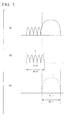
- FIG. 3 is a conceptual diagram showing frequency spectra of a reception signal, a desired signal, and an interference signal.
- the vertical axis represents power and the horizontal axis represents a frequency.
- FIG. 3(a) is a conceptual diagram showing a frequency spectrum of a signal received by the antenna 11.
- FIG. 3(b) is a conceptual diagram showing a frequency spectrum of a desired signal included in the reception signal of FIG. 3(a) .
- an "a" symbol indicates a frequency spectrum of a desired signal
- fc_d indicates a center frequency of the desired signal
- bw_d indicates a frequency bandwidth of the desired signal.
- 3(c) is a conceptual diagram showing a frequency spectrum of an interference signal included in the reception signal of FIG. 3(a) .
- an "i" symbol indicates a frequency spectrum of an interference signal
- fc_i indicates a center frequency of the interference signal
- bw_i indicates a frequency bandwidth of the interference signal.
- the filter control section 14 calculates relative positions of the desired signal and the interference signal based on the desired signal information and the interference information, and decides filter parameters to be applied to the filter 16 according to the calculation results. Specifically, the filter control section 14 selects a type of filter to be applied to the filter 16 from among a high-pass filter, a low-pass filter, and a notch filter based on the desired signal information and the interference information. The filter control section 14 decides a cutoff frequency. The filter control section 14 controls the filter 16 according to the decided filter type and cutoff frequency.
- FIGS. 4 to 8 are schematic diagrams showing the outline of a filter control process to be performed by the filter control section 14. Hereinafter, details of the filter control process will be described in detail using FIGS. 4 to 8 .
- FIG. 4 is a schematic diagram showing the outline of a filter control process when the filter control section 14 sets a low-pass filter to the filter 16.
- FIG. 4(a) is a schematic diagram showing a frequency spectrum of a signal received by the antenna 11 divided into a frequency spectrum of a desired signal and a spectrum of an interference signal.
- the vertical axis represents power
- the horizontal axis represents a frequency
- an "a" symbol indicates the frequency spectrum of the desired signal
- an "i" symbol indicates the frequency spectrum of the interference signal.
- the filter control section 14 calculates a maximum value bmax_i of a frequency band of the interference signal based on a center frequency and a frequency bandwidth of the interference signal, calculates a maximum value bmax_d of a frequency band of the desired signal based on a center frequency and a frequency bandwidth of the desired signal, and applies the low-pass filter to the filter 16 when bmax_i is higher than bmax_d ( FIG. 4(a) ).
- FIG. 4(b) is a schematic diagram showing the outline of the low-pass filter applied to the filter 16 by the filter control section 14.
- the vertical axis represents a gain (whose unit is dB), and the horizontal axis represents a frequency (whose unit is Hz).
- the filter control section 14 calculates a minimum value bmin_i of the frequency band of the interference signal based on the center frequency and the frequency bandwidth of the interference signal, and decides a value of a cutoff frequency (a frequency at which a gain of the low-pass filter becomes -3 dB) of the low-pass filter as bmin_i.
- the filter control section 14 sets parameters indicating that the filter type is the low-pass filter and the cutoff frequency is bmin_i to the filter 16 as indicated by a "u" symbol.
- FIG. 4(c) is a schematic diagram showing a frequency spectrum after the reception signal shown in FIG. 4(a) is filtered by the filter 16 in which the low-pass filter shown in FIG. 4(b) is set. As shown, the filter 16 attenuates the power of a signal having a frequency that is higher than the minimum value bmin_i of the frequency band of the interference signal, regardless of whether the signal is the desired signal or the interference signal.
- FIG. 5 is a schematic diagram showing the outline of a filter control process when the filter control section 14 sets a notch filter to the filter 16.
- FIG. 5(a) is a schematic diagram showing a frequency spectrum of a signal received by the antenna 11 divided into a frequency spectrum of a desired signal and a spectrum of an interference signal.
- the vertical axis represents power
- the horizontal axis represents a frequency
- an "a" symbol indicates the frequency spectrum of the desired signal
- an "i" symbol indicates the frequency spectrum of the interference signal.
- the filter control section 14 calculates a maximum value bmax_i and a minimum value bmin_i of a frequency band of the interference signal based on a center frequency and a frequency bandwidth of the interference signal, calculates a maximum value bmax_d and a minimum value bmax_d of a frequency band of the desired signal based on a center frequency and a frequency bandwidth of the desired signal, and applies the notch filter to the filter 16 when bmax_i is lower than bmax_d and bmin_i is higher than bmin_d ( FIG. 5(a) ).
- FIG. 5(b) is schematic diagram showing the outline of the notch filter applied to the filter 16 by the filter control section 14.
- the vertical axis represents a gain (whose unit is dB), and the horizontal axis represents a frequency (whose unit is Hz).
- the filter control section 14 calculates the minimum value bmin_i and the maximum value bmax_i of the frequency band of the interference signal based on the center frequency and the frequency bandwidth of the interference signal, and decides values of two cutoff frequencies (two frequencies at which a gain of the notch filter becomes -3 dB) of the notch filter as bmin_i and bmax_i.
- the filter control section 14 sets parameters indicating that the filter type is the notch filter and the two cutoff frequencies are bmin_i and bmax_i to the filter 16 as indicated by a "u" symbol.
- FIG. 5(c) is a schematic diagram showing a frequency spectrum after the reception signal shown in FIG. 5(a) is filtered by the filter 16 in which the notch filter shown in FIG. 5(b) is set. As shown, the filter 16 attenuates the power of a signal having a frequency between the minimum value bmin_i and the maximum value bmax_i of the frequency band of the interference signal, regardless of whether the signal is the desired signal or the interference signal.
- FIG. 6 is a schematic diagram showing the outline of a filter control process when the filter control section 14 sets a high-pass filter to the filter 16.
- FIG. 6(a) is a schematic diagram showing a frequency spectrum of a signal received by the antenna 11 divided into a frequency spectrum of a desired signal and a spectrum of an interference signal.
- the vertical axis represents power
- the horizontal axis represents a frequency
- an "a" symbol indicates the frequency spectrum of the desired signal
- an "i" symbol indicates the frequency spectrum of the interference signal.
- the filter control section 14 calculates a minimum value bmin_i of a frequency band of the interference signal based on a center frequency and a frequency bandwidth of the interference signal, calculates a minimum value bmin_d of a frequency band of the desired signal based on a center frequency and a frequency bandwidth of the desired signal, and applies the high-pass filter to the filter 16 when bmin_i is lower than bmin_d ( FIG. 6(a) ).
- FIG. 6(b) is schematic diagram showing the outline of the high-pass filter applied to the filter 16 by the filter control section 14.
- the vertical axis represents a gain (whose unit is dB), and the horizontal axis represents a frequency (whose unit is Hz).
- the filter control section 14 calculates a maximum value bmax_i of the frequency band of the interference signal based on the center frequency and the frequency bandwidth of the interference signal, and decides a value of a cutoff frequency (a frequency at which a gain of the high-pass filter becomes -3 dB) of the high-pass filter as bmax_i.
- the filter control section 14 sets parameters indicating that the filter type is the high-pass filter and the cutoff frequency is bmax_i to the filter 16 as indicated by a "u" symbol.
- FIG. 6(c) is a schematic diagram showing a frequency spectrum after the reception signal shown in FIG. 6(a) is filtered by the filter 16 in which the high-pass filter shown in FIG. 6(b) is set. As shown, the filter 16 attenuates the power of a signal having a frequency that is lower than the maximum value bmax_i of the frequency band of the interference signal, regardless of whether the signal is the desired signal or the interference signal.
- FIG. 7 is a schematic diagram showing the outline of a filter control process when the filter control section 14 sets a band-pass filter to the filter 16.
- FIG. 7(a) is a schematic diagram showing a frequency spectrum of a signal received by the antenna 11 divided into a frequency spectrum of a desired signal and a spectrum of an interference signal.
- the vertical axis represents power
- the horizontal axis represents a frequency
- an "a" symbol indicates the frequency spectrum of the desired signal
- "i1" and "i2" symbols indicate frequency spectra of interference signals.
- the filter control section 14 applies the band-pass filter to the filter 16 if frequency spectra are present at higher and lower frequencies than that of the frequency spectrum of the desired signal, for example, if both the interference signal shown in FIG. 4 and the interference signal shown in FIG. 6 are present.
- FIG. 7(b) is a schematic diagram showing the outline of the band-pass filter applied to the filter 16 by the filter control section 14.
- the vertical axis represents a gain (whose unit is dB)
- the horizontal axis represents a frequency (whose unit is Hz).
- the filter control section 14 calculates a maximum value bmax_i of a frequency band of the interference signal i1 based on a center frequency and a frequency bandwidth of the interference signal i1 of a low-frequency side, and decides a value of a cutoff frequency (a frequency at which a gain of the band-pass filter becomes -3 dB) of a low-frequency side of the band-pass filter as bmax_i1.
- the filter control section 14 calculates a minimum value bmin_i2 of a frequency band of the interference signal i2 based on a center frequency and a frequency bandwidth of the interference signal i2 of a high-frequency side, and decides a value of a cutoff frequency of a high-frequency side of the band-pass filter as bmin_i2.
- the filter control section 14 sets parameters indicating that the filter type is the band-pass filter and the cutoff frequencies are bmax_i1 and bmin_i2 to the filter 16 as indicated by a "u" symbol.
- FIG. 7(c) is a schematic diagram showing a frequency spectrum after the reception signal shown in FIG. 7(a) is filtered by the filter 16 in which the band-pass filter shown in FIG. 7(b) is set.
- the filter 16 attenuates power of a signal of a frequency that is lower than the maximum value bmax_i1 of the frequency band of the interference signal i1, and power of a signal of a frequency that is higher than the minimum value bmin_i2 of the frequency band of the interference signal i2, regardless of whether the signal is the desired signal or the interference signal.
- FIG. 8 is a schematic diagram showing the outline of a filter control process when the filter control section 14 sets a combination of a plurality of filters to the filter 16.
- FIG. 8(a) is a schematic diagram showing a frequency spectrum of a signal received by the antenna 11 divided into a frequency spectrum of a desired signal and a spectrum of an interference signal.
- the vertical axis represents power
- the horizontal axis represents a frequency
- an "a" symbol indicates the frequency spectrum of the desired signal
- "i1" and "i2" symbols indicate frequency spectra of interference signals.
- the filter control section 14 applies a combination of a low-pass filter and a band-pass filter to the filter 16 if a frequency that is higher than that of the frequency spectrum of the desired signal, and the frequency spectrum of the interference signal in the frequency spectrum of the desired signal are present, for example, if both the interference signal shown in FIG. 4 and the interference signal shown in FIG. 5 are present.
- FIG. 8(b) is a schematic diagram showing the outline of the low-pass filter and the band-pass filter applied to the filter 16 by the filter control section 14.
- the vertical axis represents a gain (whose unit is dB), and the horizontal axis represents a frequency (whose unit is Hz).
- the filter control section 14 calculates a minimum value bmin_i1 and a maximum value bmax_i1 of a frequency band of the interference signal i1 based on a center frequency and a frequency bandwidth of the interference signal i1, which is in the frequency spectrum of the desired signal, and respectively sets the minimum value bmin_i1 and the maximum value bmax_i1 as values of a cutoff frequency of the low-pass filter and a cutoff frequency of a low-frequency side of the band-pass filter.
- the filter control section 14 calculates a minimum value bmin_i2 of a frequency band of the interference signal i2 based on a center frequency and a frequency bandwidth of the interference signal i2 of a high-frequency side, and decides a value of a cutoff frequency of a high-frequency side of the band-pass filter as bmin_i2.
- the filter control section 14 sets parameters indicating that the filter type is the combination of the low-pass filter and the band-pass filter and the cutoff frequencies are respectively bmin_i1, bmax_i1, and bmin_i2 to the filter 16 as indicated by a "u" symbol.
- FIG. 8(c) is a schematic diagram showing a frequency spectrum after the reception signal shown in FIG. 8(a) is filtered by the filter 16 in which the low-pass filter and the band-pass filter shown in FIG. 8(b) are set.
- the filter 16 attenuates power of a signal of a frequency interposed between the minimum value bmin_i1 and the maximum value bmax_i1 of the frequency band of the interference signal i1 and power of a signal having a frequency that is higher than the minimum value bmin_i2 of the frequency band of the interference signal i2, regardless of whether the signal is the desired signal or the interference signal.
- FIG. 9 is a conceptual diagram showing a difference between single carrier transmission and multicarrier transmission.
- an "a" symbol indicates a frequency spectrum of a desired signal
- an "i" symbol indicates a frequency spectrum of an interference signal.
- FIG. 9(a) is a conceptual diagram when filtering is applied upon single carrier transmission.
- FIG. 9(a)-1 shows a single carrier transmission spectrum
- FIG. 9(a)-2 shows a signal spectrum upon interference
- FIG. 9(a)-3 shows a transmission spectrum after a suppression filter and a power level difference within a band by the suppression filter.
- FIG. 9(b) is a conceptual diagram of the present invention when filtering is applied upon multicarrier transmission.
- FIG. 9(b)-1 shows a multicarrier transmission spectrum
- FIG. 9(b)-2 shows a signal spectrum upon interference
- FIG. 9(b)-3 shows a transmission spectrum after a suppression filter and a power level difference within a band by the suppression filter.
- the power level difference within the band is large in the single carrier transmission, and the large power level difference within the band affects demodulation characteristics, leading to large degradation.
- a power level difference within a band of each carrier is small compared to the single carrier transmission (see KOBAYASHI, "Fundamentals and Applications of OFDM Communication Scheme, Chapter 1", Triceps, 2004), and the degradation of demodulation characteristics in each demodulator is reduced.
- FIG. 10 is a flowchart showing a processing procedure when the reception device 1 controls a filter.
- the antenna 11 receives a signal and the reception section 12 performs down-conversion and analog/digital conversion on the reception signal (step S01).
- the interference information extraction section 13 extracts interference information from the reception signal processed by the reception section 12 (step S02).
- the filter control section 14 decides a type of filter and a cutoff frequency of the filter as described above based on the interference information extracted by the interference information extraction section 13 and desired signal information stored by the filter control section 14 (step S03).
- the filter control section 14 sets the decided type and cutoff frequency of the filter to the filter 16.
- the delay section 15 delays the reception signal (step S05).
- the filter 16 attenuates power of a frequency band containing an interference signal to the reception signal by forming a filter according to parameters set in step S04 and filtering the delayed reception signal (step S06).
- the demodulation section 17 demodulates the reception signal passing through the filter 16, and generates a demodulation signal (step S07).
- the deinterleaver 18 deinterleaves the demodulation signal (step S08).
- the FEC decoding section 19 performs an FEC decoding process on the deinterleaved demodulation signal (step S09), outputs decoded reception data (step S10), and terminates the entire process of the flowchart.
- the interference information extraction section 13 extracts the interference information
- the filter control section 14 sets parameters of the filter, which attenuates a signal of a frequency band containing the interference signal, to the filter 16.
- the signal of the frequency band containing the interference signal is attenuated by the filter 16 filtering the reception signal.
- the circuit size of the interference information extraction section 13, the filter control section 14, and the filter 16 which detect a center frequency and a frequency band of the interference signal, smaller than the circuit size of a circuit for generating an interference signal replica in the related art.
- a processing time necessary for processes of the interference information extraction section 13, the filter control section 14, and the filter 16, which detect the center frequency and the frequency band of the interference signal is shorter than a processing time necessary for generating the interference signal replica in the related art. Accordingly, it is possible to reduce the effects of the interference signal while suppressing increases in circuit size and processing time.
- reception device 1 a desired signal of the frequency band containing the interference signal is also attenuated by the filter 16 along with the interference signal.
- reception data is output by the demodulation section 17 removing a guard interval from the filtered reception signal and the FEC decoding section 19 performing error correction according to FEC, the reception device 1 can generate accurate reception data even when power of some subcarriers of the desired signal is attenuated.
- the parameters set by the filter 16 are parameters decided based on interference information extracted from a reception signal received before the reception signal serving as a filtering target. Accordingly, a difference may occur between a cutoff frequency of a filter set to the filter 16 and the interference information extracted from the reception signal serving as the filtering target.
- a reception timing difference between the filtered reception signal and the reception signal referred to upon parameter decision is consistent with a processing time of the interference information extraction section 13 and the filter control section 14 and is significantly short. Because the possibility that a frequency spectrum of the interference signal will be greatly changed in the short amount of time is low, the reception accuracy of the reception device 1 is not substantially degraded even when the reception device 1 is not provided with the delay section 15. On the other hand, it is possible to shorten processing time until the FEC decoding section 19 outputs reception data after the antenna 11 receives a signal by the reception device 1 not having the delay section 15. Also, the interference information extraction process may be implemented by a method different from the interference information extraction process in the above-described embodiment.
- the reception device 1 is further provided with an auxiliary antenna having directivity to receive an interference signal arriving from a direction of the interference source 3 whose location is identified, and the interference information extraction section 13 may extract interference information from an interference signal received by the auxiliary antenna.
- the interference information extraction section 13 may extract interference information based on a frequency spectrum of a signal in which power is not allocated to a subcarrier transmitted from the transmission device 2 at a predetermined timing.
- reception device 1 may be configured as shown in the following (1) to (3).
- the present invention is applicable to a communication device which performs wireless communication.
Landscapes
- Engineering & Computer Science (AREA)
- Computer Networks & Wireless Communication (AREA)
- Signal Processing (AREA)
- Noise Elimination (AREA)
Applications Claiming Priority (2)
| Application Number | Priority Date | Filing Date | Title |
|---|---|---|---|
| JP2008192465A JP2010016785A (ja) | 2008-06-03 | 2008-07-25 | 受信装置及び受信方法 |
| PCT/JP2009/063223 WO2010010936A1 (ja) | 2008-07-25 | 2009-07-23 | 受信装置及び受信方法 |
Publications (2)
| Publication Number | Publication Date |
|---|---|
| EP2288061A1 true EP2288061A1 (de) | 2011-02-23 |
| EP2288061A4 EP2288061A4 (de) | 2011-11-16 |
Family
ID=41570396
Family Applications (1)
| Application Number | Title | Priority Date | Filing Date |
|---|---|---|---|
| EP09800450A Withdrawn EP2288061A4 (de) | 2008-07-25 | 2009-07-23 | Empfangsgerät und empfangsverfahren |
Country Status (6)
| Country | Link |
|---|---|
| US (1) | US8594255B2 (de) |
| EP (1) | EP2288061A4 (de) |
| JP (1) | JP2010016785A (de) |
| KR (2) | KR20110017006A (de) |
| CN (1) | CN102100023A (de) |
| WO (1) | WO2010010936A1 (de) |
Cited By (12)
| Publication number | Priority date | Publication date | Assignee | Title |
|---|---|---|---|---|
| US8989235B2 (en) | 2013-03-15 | 2015-03-24 | Isco International, Llc | Method and apparatus for collecting and processing interference information |
| US9198055B2 (en) | 1999-02-02 | 2015-11-24 | Isco International, Llc | Method and device for maintaining the performance quality of a communication system in the presence of narrow band interference |
| US9231650B2 (en) | 2008-11-11 | 2016-01-05 | Isco International, Llc | Method and apparatus for an adaptive filter architecture |
| WO2016064533A1 (en) * | 2014-10-24 | 2016-04-28 | Qualcomm Incorporated | Inter-rat interference cancellation |
| US9668223B2 (en) | 2014-05-05 | 2017-05-30 | Isco International, Llc | Method and apparatus for increasing performance of communication links of communication nodes |
| US10298279B2 (en) | 2017-04-05 | 2019-05-21 | Isco International, Llc | Method and apparatus for increasing performance of communication paths for communication nodes |
| US10652835B2 (en) | 2016-06-01 | 2020-05-12 | Isco International, Llc | Signal conditioning to mitigate interference impacting wireless communication links in radio access networks |
| US10680670B2 (en) | 2016-11-21 | 2020-06-09 | Sony Semiconductor Solutions Corporation | Receiving apparatus and receiving method |
| US10687284B2 (en) | 2014-05-05 | 2020-06-16 | Isco International, Llc | Method and apparatus for increasing performance of communication paths for communication nodes |
| US10833783B2 (en) | 2017-08-09 | 2020-11-10 | Isco International, Llc | Method and apparatus for monitoring, detecting, testing, diagnosing and/or mitigating interference in a communication system |
| US10892790B2 (en) | 2016-11-24 | 2021-01-12 | Sony Semiconductor Solutions Corporation | Reception apparatus and reception method |
| US11362693B2 (en) | 2017-08-09 | 2022-06-14 | Isco International, Llc | Method and apparatus for detecting and analyzing passive intermodulation interference in a communication system |
Families Citing this family (23)
| Publication number | Priority date | Publication date | Assignee | Title |
|---|---|---|---|---|
| JP2009296145A (ja) * | 2008-06-03 | 2009-12-17 | Nippon Telegr & Teleph Corp <Ntt> | 無線通信システム、無線通信方法、受信装置、及び送信装置 |
| JP5247822B2 (ja) | 2008-12-18 | 2013-07-24 | 日本電信電話株式会社 | 通信システム、送信装置、受信装置、送信方法及び通信方法 |
| JP5481679B2 (ja) * | 2010-03-16 | 2014-04-23 | 株式会社国際電気通信基礎技術研究所 | 受信装置 |
| CN102195661B (zh) * | 2010-03-18 | 2014-12-17 | 联发科技股份有限公司 | 信号处理装置以及设定信号处理装置的滤波特性的方法 |
| EP2661021B1 (de) * | 2011-12-02 | 2016-03-09 | Huawei Technologies Co., Ltd. | Verfahren zur beseitigung von nachbarkanalstörungen, modem und system dafür |
| JP5700691B2 (ja) * | 2012-01-05 | 2015-04-15 | 日本電信電話株式会社 | 受信装置、及び受信方法 |
| JP2013172331A (ja) * | 2012-02-21 | 2013-09-02 | Kddi Corp | 無線信号検出装置および無線信号検出方法 |
| CN103199885A (zh) * | 2013-04-10 | 2013-07-10 | 苏州智聚电子科技有限公司 | 大功率式无线通讯装置 |
| US9312998B2 (en) * | 2013-09-30 | 2016-04-12 | T-Mobile Usa, Inc. | Filter-based guardband determination and subcarrier selection |
| US9934681B2 (en) * | 2014-09-05 | 2018-04-03 | Halliburton Energy Services, Inc. | Electromagnetic signal booster |
| US9998235B2 (en) * | 2016-01-08 | 2018-06-12 | Google Llc | In-band optical interference mitigation for direct-detection optical communication systems |
| JP6726131B2 (ja) | 2016-04-25 | 2020-07-22 | 学校法人慶應義塾 | 無線通信システム |
| US10263685B1 (en) * | 2018-01-26 | 2019-04-16 | Zte Corporation | Intermediate frequency combiner with baseband delay |
| WO2020170221A1 (en) | 2019-02-22 | 2020-08-27 | Aerial Technologies Inc. | Handling concept drift in wi-fi-based localization |
| US11593837B2 (en) | 2019-02-22 | 2023-02-28 | Aerial Technologies Inc. | Advertisement engagement measurement |
| US11913970B2 (en) * | 2019-02-22 | 2024-02-27 | Aerial Technologies Inc. | Wireless motion detection using multiband filters |
| US11586952B2 (en) | 2019-02-22 | 2023-02-21 | Aerial Technologies Inc. | Robotic H matrix creation |
| US11082109B2 (en) | 2019-02-22 | 2021-08-03 | Aerial Technologies Inc. | Self-learning based on Wi-Fi-based monitoring and augmentation |
| US11218769B2 (en) | 2019-02-22 | 2022-01-04 | Aerial Technologies Inc. | Smart media display |
| US11448726B2 (en) | 2019-08-28 | 2022-09-20 | Aerial Technologies Inc. | System and method for presence and pulse detection from wireless signals |
| US11523253B2 (en) | 2019-09-06 | 2022-12-06 | Aerial Technologies Inc. | Monitoring activity using Wi-Fi motion detection |
| US11128432B2 (en) * | 2019-09-27 | 2021-09-21 | Huawei Technologies Co., Ltd. | Antenna system |
| CN113098579B (zh) * | 2021-02-19 | 2022-02-15 | 中国人民解放军63923部队 | 一种卫星通信隐蔽式干扰对抗的系统及方法 |
Citations (5)
| Publication number | Priority date | Publication date | Assignee | Title |
|---|---|---|---|---|
| EP0371433A2 (de) * | 1988-11-28 | 1990-06-06 | Nec Corporation | Demodulator mit Mehrfachinterferenzunterdrückung durch Korrelation zwischen unerwünschten Signalen und Fehlersignalen |
| JP2000134174A (ja) * | 1998-10-22 | 2000-05-12 | Victor Co Of Japan Ltd | Ofdm受信装置 |
| WO2007091562A1 (ja) * | 2006-02-06 | 2007-08-16 | Sony Corporation | 復調装置、方法及びプログラム |
| WO2007099413A1 (en) * | 2006-03-01 | 2007-09-07 | Nokia Corporation | Controlling a receiver to reduce influence by a predetermined interference |
| US20080143580A1 (en) * | 2006-12-15 | 2008-06-19 | Glazko Serguei A | Jammer detection and suppression for wireless communication |
Family Cites Families (13)
| Publication number | Priority date | Publication date | Assignee | Title |
|---|---|---|---|---|
| US5162805A (en) * | 1975-02-19 | 1992-11-10 | The United States Of America As Represented By The Secretary Of The Navy | Frequency diversity sidelobe canceller |
| US4736455A (en) * | 1985-12-23 | 1988-04-05 | Nippon Telegraph And Telephone Corporation | Interference cancellation system |
| JPH04360441A (ja) * | 1991-06-07 | 1992-12-14 | Nippon Telegr & Teleph Corp <Ntt> | 干渉補償方式 |
| JP3273861B2 (ja) * | 1994-06-13 | 2002-04-15 | 富士通テン株式会社 | テレビジョン受信装置 |
| JP3538187B2 (ja) * | 2002-03-26 | 2004-06-14 | 株式会社東芝 | Ofdm受信装置およびofdm受信装置におけるデータ復調方法 |
| NZ526669A (en) * | 2003-06-25 | 2006-03-31 | Ind Res Ltd | Narrowband interference suppression for OFDM systems |
| JP4421416B2 (ja) | 2004-08-04 | 2010-02-24 | 富士通株式会社 | Ofdm方式の受信装置 |
| WO2006090742A1 (ja) * | 2005-02-22 | 2006-08-31 | Tadashi Asahina | 符号型送信装置及び符号型受信装置 |
| US7761075B2 (en) | 2005-09-21 | 2010-07-20 | Samsung Electronics Co., Ltd. | Apparatus and method for interference cancellation in wireless mobile stations operating concurrently on two or more air interfaces |
| JP2007243662A (ja) * | 2006-03-09 | 2007-09-20 | Matsushita Electric Ind Co Ltd | 周波数可変フィルタ回路 |
| NZ552270A (en) * | 2006-12-21 | 2008-10-31 | Ind Res Ltd | Detection of wideband interference |
| JP4751841B2 (ja) | 2007-02-05 | 2011-08-17 | 財団法人高知県産業振興センター | 電界放出型電極及び電子機器 |
| JP5247822B2 (ja) * | 2008-12-18 | 2013-07-24 | 日本電信電話株式会社 | 通信システム、送信装置、受信装置、送信方法及び通信方法 |
-
2008
- 2008-07-25 JP JP2008192465A patent/JP2010016785A/ja active Pending
-
2009
- 2009-07-23 KR KR1020117000897A patent/KR20110017006A/ko active Application Filing
- 2009-07-23 US US13/003,810 patent/US8594255B2/en not_active Expired - Fee Related
- 2009-07-23 EP EP09800450A patent/EP2288061A4/de not_active Withdrawn
- 2009-07-23 KR KR1020137003314A patent/KR20130031381A/ko not_active Application Discontinuation
- 2009-07-23 CN CN2009801274504A patent/CN102100023A/zh active Pending
- 2009-07-23 WO PCT/JP2009/063223 patent/WO2010010936A1/ja active Application Filing
Patent Citations (5)
| Publication number | Priority date | Publication date | Assignee | Title |
|---|---|---|---|---|
| EP0371433A2 (de) * | 1988-11-28 | 1990-06-06 | Nec Corporation | Demodulator mit Mehrfachinterferenzunterdrückung durch Korrelation zwischen unerwünschten Signalen und Fehlersignalen |
| JP2000134174A (ja) * | 1998-10-22 | 2000-05-12 | Victor Co Of Japan Ltd | Ofdm受信装置 |
| WO2007091562A1 (ja) * | 2006-02-06 | 2007-08-16 | Sony Corporation | 復調装置、方法及びプログラム |
| WO2007099413A1 (en) * | 2006-03-01 | 2007-09-07 | Nokia Corporation | Controlling a receiver to reduce influence by a predetermined interference |
| US20080143580A1 (en) * | 2006-12-15 | 2008-06-19 | Glazko Serguei A | Jammer detection and suppression for wireless communication |
Non-Patent Citations (2)
| Title |
|---|
| FAZEL K: "Narrow-band interference rejection in orthogonal multi-carrier spread-spectrum communications", UNIVERSAL PERSONAL COMMUNICATIONS, 1994. RECORD., 1994 THIRD ANNUAL IN TERNATIONAL CONFERENCE ON SAN DIEGO, CA, USA 27 SEPT.-1 OCT. 1994, NEW YORK, NY, USA,IEEE, 27 September 1994 (1994-09-27), pages 46-50, XP010131551, DOI: 10.1109/ICUPC.1994.383042 ISBN: 978-0-7803-1823-6 * |
| See also references of WO2010010936A1 * |
Cited By (134)
| Publication number | Priority date | Publication date | Assignee | Title |
|---|---|---|---|---|
| US9215719B2 (en) | 1999-02-02 | 2015-12-15 | Isco International, Llc | Method and device for maintaining the performance quality of a communication system in the presence of narrow band interference |
| US9894662B2 (en) | 1999-02-02 | 2018-02-13 | Isco International, Llc | Method and device for maintaining the performance quality of a communication system in the presence of narrow band interference |
| US9451495B2 (en) | 1999-02-02 | 2016-09-20 | Isco International, Llc | Method and device for maintaining the performance quality of a communication system in the presence of narrow band interference |
| US10039117B2 (en) | 1999-02-02 | 2018-07-31 | Isco International, Llc | Method and device for maintaining the performance quality of a communication system in the presence of narrow band interference |
| US9215723B2 (en) | 1999-02-02 | 2015-12-15 | Isco International, Llc | Method and device for maintaining the performance quality of a communication system in the presence of narrow band interference |
| US9788331B2 (en) | 1999-02-02 | 2017-10-10 | Isco International, Llc | Method and device for maintaining the performance quality of a communication system in the presence of narrow band interference |
| US9198055B2 (en) | 1999-02-02 | 2015-11-24 | Isco International, Llc | Method and device for maintaining the performance quality of a communication system in the presence of narrow band interference |
| US9247553B2 (en) | 1999-02-02 | 2016-01-26 | Isco International, Llc | Method and device for maintaining the performance quality of a communication system in the presence of narrow band interference |
| US9232423B2 (en) | 1999-02-02 | 2016-01-05 | Isco International, Llc | Method and device for maintaining the performance quality of a communication system in the presence of narrow band interference |
| US9706559B2 (en) | 1999-02-02 | 2017-07-11 | Isco International, Llc | Method and device for maintaining the performance quality of a communication system in the presence of narrow band interference |
| US10461802B2 (en) | 2008-11-11 | 2019-10-29 | Isco International, Llc | Method and apparatus for an adaptive filter architecture |
| US9231650B2 (en) | 2008-11-11 | 2016-01-05 | Isco International, Llc | Method and apparatus for an adaptive filter architecture |
| US10097235B2 (en) | 2008-11-11 | 2018-10-09 | Isco International, Llc | Method and apparatus for an adaptive filter architecture |
| US9654170B2 (en) | 2008-11-11 | 2017-05-16 | Isco International, Llc | Method and apparatus for an adaptive filter architecture |
| US9647720B2 (en) | 2008-11-11 | 2017-05-09 | Isco International, Llc | Method and apparatus for an adaptive filter architecture |
| US9281864B2 (en) | 2008-11-11 | 2016-03-08 | Isco International, Llc | Method and apparatus for an adaptive filter architecture |
| US9294144B2 (en) | 2008-11-11 | 2016-03-22 | Isco International, Llc | Method and apparatus for an adaptive filter architecture |
| US9832000B2 (en) | 2013-03-15 | 2017-11-28 | Isco International, Llc | Method and apparatus for signal interference processing |
| US10063361B2 (en) | 2013-03-15 | 2018-08-28 | Isco International, Llc | Method and apparatus for signal interference processing |
| US11950270B2 (en) | 2013-03-15 | 2024-04-02 | Isco International, Llc | Method and apparatus for collecting and processing interference information |
| US9357426B2 (en) | 2013-03-15 | 2016-05-31 | Isco International, Llc | Method and apparatus for avoiding interference |
| US9369909B2 (en) | 2013-03-15 | 2016-06-14 | Isco International, Llc | Method and apparatus for mitigating signal interference in a feedback system |
| US9426692B2 (en) | 2013-03-15 | 2016-08-23 | Isco International, Llc | Creating library of interferers |
| US9313680B2 (en) | 2013-03-15 | 2016-04-12 | Isco International, Llc | Method and apparatus for signal interference processing |
| US9634819B2 (en) | 2013-03-15 | 2017-04-25 | Isco International, Llc | Method and apparatus for signal interference processing |
| US11711839B2 (en) | 2013-03-15 | 2023-07-25 | Isco International, Llc | Method and apparatus for avoiding interference |
| US9271185B2 (en) | 2013-03-15 | 2016-02-23 | Isco International, Llc | Method and apparatus for interference mitigation utilizing antenna pattern adjustments |
| US9214983B2 (en) | 2013-03-15 | 2015-12-15 | Isco International, Llc | Method and apparatus for collecting and processing interference information |
| US11653374B2 (en) | 2013-03-15 | 2023-05-16 | Isco International, Llc | Method and apparatus for signal interference processing |
| US9209857B2 (en) | 2013-03-15 | 2015-12-08 | Isco International, Llc | Method and apparatus for signal interference processing |
| US9729301B2 (en) | 2013-03-15 | 2017-08-08 | Isco International, Llc | Method and apparatus for mitigating signal interference in a feedback system |
| US9729196B2 (en) | 2013-03-15 | 2017-08-08 | Isco International, Llc | Method and apparatus for avoiding interference |
| US9742547B2 (en) | 2013-03-15 | 2017-08-22 | Isco International, Llc | Method and apparatus for signal interference processing |
| US9749114B2 (en) | 2013-03-15 | 2017-08-29 | Isco International, Llc | Method and apparatus for signal interference processing |
| US11638268B2 (en) | 2013-03-15 | 2023-04-25 | Isco International, Llc | Method and apparatus for interference mitigation utilizing antenna pattern adjustments |
| US9112594B2 (en) | 2013-03-15 | 2015-08-18 | Isco International, Llc | Method and apparatus for signal interference avoidance |
| US11582763B2 (en) | 2013-03-15 | 2023-02-14 | Isco International, Llc | Creating library of interferers |
| US10652903B2 (en) | 2013-03-15 | 2020-05-12 | Isco International, Llc | Method and apparatus for interference mitigation utilizing antenna pattern adjustments |
| US9077443B2 (en) | 2013-03-15 | 2015-07-07 | Isco International, Llc | Method and apparatus for signal interference processing |
| US11445517B2 (en) | 2013-03-15 | 2022-09-13 | Isco International, Llc | Method and apparatus for signal interference processing |
| US9961691B2 (en) | 2013-03-15 | 2018-05-01 | Isco International, Llc | Method and apparatus for avoiding interference |
| US11375516B2 (en) | 2013-03-15 | 2022-06-28 | Isco International, Llc | Method and apparatus for signal interference avoidance |
| US9992008B2 (en) | 2013-03-15 | 2018-06-05 | Isco International, Llc | Creating library of interferers |
| US11304204B2 (en) | 2013-03-15 | 2022-04-12 | Isco International, Llc | Method and apparatus for signal interference processing |
| US9071343B2 (en) | 2013-03-15 | 2015-06-30 | Isco International, Llc | Method and apparatus for avoiding interference |
| US10050763B2 (en) | 2013-03-15 | 2018-08-14 | Isco International, Llc | Method and apparatus for signal interference avoidance |
| US9319916B2 (en) | 2013-03-15 | 2016-04-19 | Isco International, Llc | Method and appartus for signal interference processing |
| US10079667B2 (en) | 2013-03-15 | 2018-09-18 | Isco International, Llc | Method and apparatus for signal interference processing |
| US9042497B2 (en) | 2013-03-15 | 2015-05-26 | Isco International, Llc | Method and apparatus for mitigating signal interference in a feedback system |
| US11191086B2 (en) | 2013-03-15 | 2021-11-30 | Isco International, Llc | Method and apparatus for mitigating signal interference in a feedback system |
| US10129003B2 (en) | 2013-03-15 | 2018-11-13 | Isco International, Llc | Method and apparatus for interference mitigation utilizing antenna pattern adjustments |
| US11166288B2 (en) | 2013-03-15 | 2021-11-02 | Isco International, Llc | Method and apparatus for collecting and processing interference information |
| US10187190B2 (en) | 2013-03-15 | 2019-01-22 | Isco International, Llc | Method and apparatus for collecting and processing interference information |
| US10225063B2 (en) | 2013-03-15 | 2019-03-05 | Isco International, Llc | Method and apparatus for avoiding interference |
| US11134502B2 (en) | 2013-03-15 | 2021-09-28 | Isco International, Llc | Method and apparatus for interference mitigation utilizing antenna pattern adjustments |
| US11115988B2 (en) | 2013-03-15 | 2021-09-07 | Isco International, Llc | Method and apparatus for avoiding interference |
| US10278192B2 (en) | 2013-03-15 | 2019-04-30 | Isco International, Llc | Method and apparatus for signal interference processing |
| US10945271B2 (en) | 2013-03-15 | 2021-03-09 | Isco International, Llc | Creating library of interferers |
| US10313087B2 (en) | 2013-03-15 | 2019-06-04 | Isco International, Llc | Method and apparatus for signal interference processing |
| US10327255B2 (en) | 2013-03-15 | 2019-06-18 | Isco International, Llc | Method and apparatus for signal interference processing |
| US10904890B2 (en) | 2013-03-15 | 2021-01-26 | Isco International, Llc | Method and apparatus for signal interference processing |
| US10420114B2 (en) | 2013-03-15 | 2019-09-17 | Isco International, Llc | Method and apparatus for signal interference processing |
| US10419195B2 (en) | 2013-03-15 | 2019-09-17 | Isco International, Llc | Creating library of interferers |
| US10880902B2 (en) | 2013-03-15 | 2020-12-29 | Isco International, Llc | Method and apparatus for signal interference processing |
| US9008680B2 (en) | 2013-03-15 | 2015-04-14 | Isco International, Llc | Method and apparatus for signal interference processing |
| US10880901B2 (en) | 2013-03-15 | 2020-12-29 | Isco International, Llc | Method and apparatus for mitigating signal interference in a feedback system |
| US10841928B2 (en) | 2013-03-15 | 2020-11-17 | Isco International, Llc | Method and apparatus for signal interference processing |
| US8989235B2 (en) | 2013-03-15 | 2015-03-24 | Isco International, Llc | Method and apparatus for collecting and processing interference information |
| US10517101B2 (en) | 2013-03-15 | 2019-12-24 | Isco International, Llc | Method and apparatus for mitigating signal interference in a feedback system |
| US10805937B2 (en) | 2013-03-15 | 2020-10-13 | Isco International, Llc | Method and apparatus for avoiding interference |
| US10560952B2 (en) | 2013-03-15 | 2020-02-11 | Isco International, Llc | Creating library of interferers |
| US10798718B2 (en) | 2013-03-15 | 2020-10-06 | Isco International, Llc | Method and apparatus for collecting and processing interference information |
| US10582510B2 (en) | 2013-03-15 | 2020-03-03 | Isco International, Llc | Method and apparatus for avoiding interference |
| US10582511B2 (en) | 2013-03-15 | 2020-03-03 | Isco International, Llc | Method and apparatus for signal interference processing |
| US10667275B2 (en) | 2013-03-15 | 2020-05-26 | Isco International, Llc | Method and apparatus for signal interference avoidance |
| US10652901B2 (en) | 2013-03-15 | 2020-05-12 | Isco International, Llc | Method and apparatus for signal interference processing |
| US10512044B2 (en) | 2014-05-05 | 2019-12-17 | Isco International, Llc | Method and apparatus for increasing performance of communication links of communication nodes |
| US9912433B2 (en) | 2014-05-05 | 2018-03-06 | Isco International, Llc | Method and apparatus for increasing performance of communication links of communication nodes |
| US10609651B2 (en) | 2014-05-05 | 2020-03-31 | Isco International, Llc | Adjusting signal power to increase performance of communication links of communication nodes |
| US11877247B2 (en) | 2014-05-05 | 2024-01-16 | Isco International, Llc | Method and apparatus for increasing performance of communication links of cooperative communication nodes |
| US9668223B2 (en) | 2014-05-05 | 2017-05-30 | Isco International, Llc | Method and apparatus for increasing performance of communication links of communication nodes |
| US9775116B2 (en) | 2014-05-05 | 2017-09-26 | Isco International, Llc | Method and apparatus for increasing performance of communication links of cooperative communication nodes |
| US10687284B2 (en) | 2014-05-05 | 2020-06-16 | Isco International, Llc | Method and apparatus for increasing performance of communication paths for communication nodes |
| US9794888B2 (en) | 2014-05-05 | 2017-10-17 | Isco International, Llc | Method and apparatus for increasing performance of a communication link of a communication node |
| US10575260B2 (en) | 2014-05-05 | 2020-02-25 | Isco International, Llc | Method and apparatus for increasing performance of communication links of cooperative communication nodes |
| US11570719B2 (en) | 2014-05-05 | 2023-01-31 | Isco International, Llc | Method and apparatus for increasing performance of communication links of cooperative communication nodes |
| US10820282B2 (en) | 2014-05-05 | 2020-10-27 | Isco International, Llc | Method and apparatus for increasing performance of a communication link of a communication node |
| US10834684B2 (en) | 2014-05-05 | 2020-11-10 | Isco International, Llc | Adjusting signal power to increase performance of communication links of communication nodes |
| US10834683B2 (en) | 2014-05-05 | 2020-11-10 | Isco International, Llc | Method and apparatus for increasing performance of communication links of communication nodes |
| US11412457B2 (en) | 2014-05-05 | 2022-08-09 | Isco International, Llc | Adjusting signal power to increase performance of communication links of communication nodes |
| US10506526B2 (en) | 2014-05-05 | 2019-12-10 | Isco International, Llc | Method and apparatus for increasing performance of a communication link of a communication node |
| US9986512B2 (en) | 2014-05-05 | 2018-05-29 | Isco International, Llc | Method and apparatus for mitigating interference |
| US11330531B2 (en) | 2014-05-05 | 2022-05-10 | Isco International, Llc | Method and apparatus for increasing performance of communication links of communication nodes |
| US10425903B2 (en) | 2014-05-05 | 2019-09-24 | Isco International, Llc | Method and apparatus for mitigating interference |
| US10039061B2 (en) | 2014-05-05 | 2018-07-31 | Isco International, Llc | Method and apparatus for increasing performance of communication links of cooperative communication nodes |
| US11197247B2 (en) | 2014-05-05 | 2021-12-07 | Isco International, Llc | Method and apparatus for increasing performance of communication paths for communication nodes |
| US10097301B2 (en) | 2014-05-05 | 2018-10-09 | Isco International, Llc | Method and apparatus for increasing performance of communication links of communication nodes |
| US10178628B2 (en) | 2014-05-05 | 2019-01-08 | Isco International, Llc | Method and apparatus for increasing performance of communication paths for communication nodes |
| US10231190B2 (en) | 2014-05-05 | 2019-03-12 | Isco International, Llc | Method and apparatus for increasing performance of communication links of cooperative communication nodes |
| US10244483B2 (en) | 2014-05-05 | 2019-03-26 | Isco International, Llc | Method and apparatus for increasing performance of a communication link of a communication node |
| US10959185B2 (en) | 2014-05-05 | 2021-03-23 | Isco International, Llc | Method and apparatus for increasing performance of communication links of cooperative communication nodes |
| WO2016064533A1 (en) * | 2014-10-24 | 2016-04-28 | Qualcomm Incorporated | Inter-rat interference cancellation |
| US9641272B2 (en) | 2014-10-24 | 2017-05-02 | Qualcomm Incorporated | Inter-rat interference cancellation |
| US10952155B2 (en) | 2016-06-01 | 2021-03-16 | Isco International, Llc | Method and apparatus for performing signal conditioning to mitigate interference detected in a communication system |
| US10652835B2 (en) | 2016-06-01 | 2020-05-12 | Isco International, Llc | Signal conditioning to mitigate interference impacting wireless communication links in radio access networks |
| US11277803B2 (en) | 2016-06-01 | 2022-03-15 | Isco International, Llc | Signal conditioning to mitigate interference |
| US10680670B2 (en) | 2016-11-21 | 2020-06-09 | Sony Semiconductor Solutions Corporation | Receiving apparatus and receiving method |
| US10892790B2 (en) | 2016-11-24 | 2021-01-12 | Sony Semiconductor Solutions Corporation | Reception apparatus and reception method |
| US11411590B2 (en) | 2017-04-05 | 2022-08-09 | Isco International, Llc | Correlating network and physical layer activities |
| US10992330B2 (en) | 2017-04-05 | 2021-04-27 | Isco International, Llc | Methods and apparatus for packet testing and isolation of interference in a multi-layered protocol |
| US10892789B2 (en) | 2017-04-05 | 2021-01-12 | Isco International, Llc | Methods, systems, and devices for adjusting resource block schedules for user end devices to different frequency bands |
| US10396838B2 (en) | 2017-04-05 | 2019-08-27 | Isco International, Llc | Methods, systems and devices to improve channel utilization |
| US11139846B2 (en) | 2017-04-05 | 2021-10-05 | Isco International, Llc | Method and apparatus for increasing performance of communication paths for communication nodes |
| US10886957B2 (en) | 2017-04-05 | 2021-01-05 | Isco International, Llc | Correlating network and physical layer activities |
| US10879945B2 (en) | 2017-04-05 | 2020-12-29 | Isco International, Llc | Methods, systems and devices to improve channel utilization |
| US10979093B2 (en) | 2017-04-05 | 2021-04-13 | Isco International, Llc | Method and apparatus for real-time monitoring and field adjustment |
| US10491252B2 (en) | 2017-04-05 | 2019-11-26 | Isco International, Llc | Method and apparatus for mitigating interference in CPRI uplink paths |
| US10979092B2 (en) | 2017-04-05 | 2021-04-13 | Isco International, Llc | Method and apparatus for mitigating interference in CPRI uplink paths |
| US10659093B2 (en) | 2017-04-05 | 2020-05-19 | Isco International, Llc | Managing interference in control channels and methods thereof |
| US10298279B2 (en) | 2017-04-05 | 2019-05-21 | Isco International, Llc | Method and apparatus for increasing performance of communication paths for communication nodes |
| US11456766B2 (en) | 2017-04-05 | 2022-09-27 | Isco International, Llc | Virtualized methods, systems and devices to mitigate channel interference |
| US11502711B2 (en) | 2017-04-05 | 2022-11-15 | Isco International, Llc | Methods, systems and devices to improve channel utilization |
| US10523252B2 (en) | 2017-04-05 | 2019-12-31 | Isco International, Llc | Method and apparatus for real-time monitoring and field adjustment |
| US10797740B2 (en) | 2017-04-05 | 2020-10-06 | Isco International, Llc | Virtualized methods, systems and devices to mitigate channel interference |
| US11601149B2 (en) | 2017-04-05 | 2023-03-07 | Isco International, Llc | Method and apparatus for real-time monitoring and field adjustment |
| US11075660B2 (en) | 2017-04-05 | 2021-07-27 | Isco International, Llc | Managing interference in control channels and methods thereof |
| US10594347B2 (en) | 2017-04-05 | 2020-03-17 | Isco International, Llc | Methods, systems and devices to improve channel utilization |
| US11855670B2 (en) | 2017-04-05 | 2023-12-26 | Isco International, Llc | Method and apparatus for real-time monitoring and field adjustment |
| US11722164B2 (en) | 2017-04-05 | 2023-08-08 | Isco International, Llc | Correlating network and physical layer activities |
| US11770147B2 (en) | 2017-04-05 | 2023-09-26 | Isco International, Llc | Method and apparatus for increasing performance of communication paths for communication nodes |
| US11728912B2 (en) | 2017-08-09 | 2023-08-15 | Isco International, Llc | Method and apparatus for monitoring, detecting, testing, diagnosing and/or mitigating interference in a communication system |
| US11184094B2 (en) | 2017-08-09 | 2021-11-23 | Isco International, Llc | Method and apparatus for monitoring, detecting, testing, diagnosing and/or mitigating interference in a communication system |
| US10833783B2 (en) | 2017-08-09 | 2020-11-10 | Isco International, Llc | Method and apparatus for monitoring, detecting, testing, diagnosing and/or mitigating interference in a communication system |
| US11362693B2 (en) | 2017-08-09 | 2022-06-14 | Isco International, Llc | Method and apparatus for detecting and analyzing passive intermodulation interference in a communication system |
Also Published As
| Publication number | Publication date |
|---|---|
| KR20110017006A (ko) | 2011-02-18 |
| US20110129047A1 (en) | 2011-06-02 |
| WO2010010936A1 (ja) | 2010-01-28 |
| CN102100023A (zh) | 2011-06-15 |
| JP2010016785A (ja) | 2010-01-21 |
| US8594255B2 (en) | 2013-11-26 |
| EP2288061A4 (de) | 2011-11-16 |
| KR20130031381A (ko) | 2013-03-28 |
Similar Documents
| Publication | Publication Date | Title |
|---|---|---|
| EP2288061A1 (de) | Empfangsgerät und empfangsverfahren | |
| EP2676377B1 (de) | Satellitenempfänger mit interferierender signalunterdrückung | |
| JP4983365B2 (ja) | 無線通信装置 | |
| CA2483856A1 (en) | Adjacent channel interference mitigation for fm digital audio broadcasting receivers | |
| WO2008145799A1 (en) | Interference in communication devices | |
| JP6166086B2 (ja) | 受信機および信号処理方法 | |
| WO2012177690A1 (en) | Method and apparatus for implementing signal quality metrics and antenna diversity switching control | |
| WO2015087731A1 (ja) | 受信装置 | |
| JP4352082B2 (ja) | 周波数同期回路、方法、プログラム及びこれらを用いた受信装置 | |
| US10149263B2 (en) | Techniques for transmitting/receiving portions of received signal to identify preamble portion and to determine signal-distorting characteristics | |
| US8537713B2 (en) | Carrier frequency acquisition method and apparatus having improved reliability for detecting carrier acquisition or loss thereof | |
| EP3090489A1 (de) | Verfahren zur einstellung von lo-frequenzen bei einem empfänger und zugehöriger empfänger | |
| US9369217B1 (en) | Cellular up-link harmonic spurs mitigation in Wi-Fi and bluetooth receivers | |
| JP2009159452A (ja) | 干渉抑圧システム及び異種無線通信システム間における干渉抑圧方法 | |
| WO2011018927A1 (ja) | 無線通信システム、無線通信装置および無線通信方法 | |
| Berardinelli et al. | An SDR architecture for OFDM transmission over USRP2 boards | |
| KR100530262B1 (ko) | 무선 랜 시스템의 위상잡음 제거 장치 및 그 방법 | |
| EP3382899A1 (de) | Empfänger für niedrige zwischenfrequenz | |
| US11381267B1 (en) | System, apparatus and method for cancelling tonal interference in an orthogonal frequency division multiplexing (OFDM) receiver | |
| JP5873427B2 (ja) | 伝送路推定器、受信装置及び伝送路推定方法 | |
| Wang et al. | Design and Implementation of Time-Domain Interference Cancellation Receiver for LTE-U Systems | |
| JP2011199480A (ja) | 受信機、及びこれに用いるフレーム復調方法 | |
| JP2010268375A (ja) | パケット無線通信受信端末 | |
| JP2012175442A (ja) | Ofdm受信装置 | |
| JP2008245064A (ja) | 受信装置、送信装置および通信方法 |
Legal Events
| Date | Code | Title | Description |
|---|---|---|---|
| PUAI | Public reference made under article 153(3) epc to a published international application that has entered the european phase |
Free format text: ORIGINAL CODE: 0009012 |
|
| 17P | Request for examination filed |
Effective date: 20110112 |
|
| AK | Designated contracting states |
Kind code of ref document: A1 Designated state(s): AT BE BG CH CY CZ DE DK EE ES FI FR GB GR HR HU IE IS IT LI LT LU LV MC MK MT NL NO PL PT RO SE SI SK SM TR |
|
| AX | Request for extension of the european patent |
Extension state: AL BA RS |
|
| DAX | Request for extension of the european patent (deleted) | ||
| A4 | Supplementary search report drawn up and despatched |
Effective date: 20111013 |
|
| RIC1 | Information provided on ipc code assigned before grant |
Ipc: H04L 27/26 20060101ALI20111008BHEP Ipc: H04B 1/10 20060101AFI20111008BHEP |
|
| 17Q | First examination report despatched |
Effective date: 20130104 |
|
| GRAP | Despatch of communication of intention to grant a patent |
Free format text: ORIGINAL CODE: EPIDOSNIGR1 |
|
| INTG | Intention to grant announced |
Effective date: 20140113 |
|
| STAA | Information on the status of an ep patent application or granted ep patent |
Free format text: STATUS: THE APPLICATION IS DEEMED TO BE WITHDRAWN |
|
| 18D | Application deemed to be withdrawn |
Effective date: 20140514 |