EP2286469B1 - Halbleiterkörper und verfahren zur herstellung eines halbleiterkörpers - Google Patents
Halbleiterkörper und verfahren zur herstellung eines halbleiterkörpers Download PDFInfo
- Publication number
- EP2286469B1 EP2286469B1 EP09761309A EP09761309A EP2286469B1 EP 2286469 B1 EP2286469 B1 EP 2286469B1 EP 09761309 A EP09761309 A EP 09761309A EP 09761309 A EP09761309 A EP 09761309A EP 2286469 B1 EP2286469 B1 EP 2286469B1
- Authority
- EP
- European Patent Office
- Prior art keywords
- semiconductor layer
- type semiconductor
- conducting
- layer
- semiconductor body
- Prior art date
- Legal status (The legal status is an assumption and is not a legal conclusion. Google has not performed a legal analysis and makes no representation as to the accuracy of the status listed.)
- Active
Links
Images


Classifications
-
- H—ELECTRICITY
- H10—SEMICONDUCTOR DEVICES; ELECTRIC SOLID-STATE DEVICES NOT OTHERWISE PROVIDED FOR
- H10H—INORGANIC LIGHT-EMITTING SEMICONDUCTOR DEVICES HAVING POTENTIAL BARRIERS
- H10H20/00—Individual inorganic light-emitting semiconductor devices having potential barriers, e.g. light-emitting diodes [LED]
- H10H20/80—Constructional details
- H10H20/81—Bodies
- H10H20/8215—Bodies characterised by crystalline imperfections, e.g. dislocations; characterised by the distribution of dopants, e.g. delta-doping
-
- H—ELECTRICITY
- H10—SEMICONDUCTOR DEVICES; ELECTRIC SOLID-STATE DEVICES NOT OTHERWISE PROVIDED FOR
- H10H—INORGANIC LIGHT-EMITTING SEMICONDUCTOR DEVICES HAVING POTENTIAL BARRIERS
- H10H20/00—Individual inorganic light-emitting semiconductor devices having potential barriers, e.g. light-emitting diodes [LED]
- H10H20/80—Constructional details
- H10H20/81—Bodies
- H10H20/816—Bodies having carrier transport control structures, e.g. highly-doped semiconductor layers or current-blocking structures
-
- H—ELECTRICITY
- H10—SEMICONDUCTOR DEVICES; ELECTRIC SOLID-STATE DEVICES NOT OTHERWISE PROVIDED FOR
- H10H—INORGANIC LIGHT-EMITTING SEMICONDUCTOR DEVICES HAVING POTENTIAL BARRIERS
- H10H20/00—Individual inorganic light-emitting semiconductor devices having potential barriers, e.g. light-emitting diodes [LED]
- H10H20/80—Constructional details
- H10H20/81—Bodies
- H10H20/822—Materials of the light-emitting regions
- H10H20/824—Materials of the light-emitting regions comprising only Group III-V materials, e.g. GaP
- H10H20/825—Materials of the light-emitting regions comprising only Group III-V materials, e.g. GaP containing nitrogen, e.g. GaN
- H10H20/8252—Materials of the light-emitting regions comprising only Group III-V materials, e.g. GaP containing nitrogen, e.g. GaN characterised by the dopants
-
- H—ELECTRICITY
- H01—ELECTRIC ELEMENTS
- H01S—DEVICES USING THE PROCESS OF LIGHT AMPLIFICATION BY STIMULATED EMISSION OF RADIATION [LASER] TO AMPLIFY OR GENERATE LIGHT; DEVICES USING STIMULATED EMISSION OF ELECTROMAGNETIC RADIATION IN WAVE RANGES OTHER THAN OPTICAL
- H01S5/00—Semiconductor lasers
- H01S5/30—Structure or shape of the active region; Materials used for the active region
- H01S5/305—Structure or shape of the active region; Materials used for the active region characterised by the doping materials used in the laser structure
-
- H—ELECTRICITY
- H10—SEMICONDUCTOR DEVICES; ELECTRIC SOLID-STATE DEVICES NOT OTHERWISE PROVIDED FOR
- H10H—INORGANIC LIGHT-EMITTING SEMICONDUCTOR DEVICES HAVING POTENTIAL BARRIERS
- H10H20/00—Individual inorganic light-emitting semiconductor devices having potential barriers, e.g. light-emitting diodes [LED]
- H10H20/01—Manufacture or treatment
-
- H—ELECTRICITY
- H10—SEMICONDUCTOR DEVICES; ELECTRIC SOLID-STATE DEVICES NOT OTHERWISE PROVIDED FOR
- H10H—INORGANIC LIGHT-EMITTING SEMICONDUCTOR DEVICES HAVING POTENTIAL BARRIERS
- H10H20/00—Individual inorganic light-emitting semiconductor devices having potential barriers, e.g. light-emitting diodes [LED]
- H10H20/80—Constructional details
- H10H20/81—Bodies
- H10H20/811—Bodies having quantum effect structures or superlattices, e.g. tunnel junctions
- H10H20/812—Bodies having quantum effect structures or superlattices, e.g. tunnel junctions within the light-emitting regions, e.g. having quantum confinement structures
Definitions
- the present application relates to a semiconductor body and a method for producing a semiconductor body.
- semiconductor layers which are doped with magnesium for a p-type conductivity are often used.
- the semiconductor layers may be subjected to an activation step in which hydrogen incorporated into the layer is separated from the magnesium.
- an activation step in which hydrogen incorporated into the layer is separated from the magnesium.
- insufficient activation of the magnesium can lead to an increased operating voltage of the light-emitting diode.
- the p-type semiconductor layer should have an improved degree of activation. Furthermore, a method for producing a semiconductor body is to be specified.
- a semiconductor body has an n-type semiconductor layer and a p-type Semiconductor layer on.
- the p-type semiconductor layer contains a p-type impurity.
- the n-type semiconductor layer contains an n-type dopant and another dopant.
- the degree of activation of the p-type semiconductor layer is permanently increased. That is, the proportion of the atoms of the p-type impurity providing holes as carriers is increased.
- the n-type semiconductor layer may have an at least locally increased permeability to hydrogen.
- the solubility of hydrogen in the n-type semiconductor layer may be increased by means of the further dopant.
- hydrogen may pass through the n-type semiconductor layer disposed over the p-type layer. The diffusion of hydrogen through the n-type semiconductor layer can thus be facilitated by the further dopant.
- an active region provided for generating radiation and / or a tunnel junction is formed between the p-type semiconductor layer and the n-type semiconductor layer.
- the functional pn junction serves either to generate radiation - in the case of the active region - or to electrically connect a p-doped layer to an n-doped layer - in the case of the tunnel junction.
- the tunnel junction may have, for example, a highly p-doped tunnel layer and a highly n-doped tunnel layer.
- the pervious semiconductor layer is covered by at least one further semiconductor layer.
- the further semiconductor layer may be, for example, a semiconductor layer with the active region provided for the generation of radiation or with the tunnel junction.
- the p-type semiconductor layer is then buried and is not located on an outside of the semiconductor body. That is, the p-type semiconductor layer is not exposed.
- the p-type semiconductor layer is arranged between the active region and a carrier or a growth substrate.
- the n-type semiconductor layer with the n-type dopant and the further dopant is then arranged.
- the p-type semiconductor layer is then buried and not freely accessible from outside the semiconductor body.
- the n-type semiconductor layer has a thickness of at least 5 nm, preferably at least 10 nm, particularly preferably at least 20 nm.
- Such an n-type semiconductor layer without further dopant, that is, only with an n-type dopant, is impermeable to hydrogen. Only by the addition of the further dopant is a permeability of the layer for hydrogen achieved.
- the n-type semiconductor layer may in this case be formed thicker than 20 nm, which for example improves the transverse conductivity of the n-type semiconductor layer.
- the semiconductor body is preferably based on a nitride compound semiconductor material.
- Niride compound semiconductors based in the present context means that the active epitaxial layer sequence or at least one layer thereof comprises a nitride III / V compound semiconductor material, preferably Al n Ga m In 1 nm N, where 0 ⁇ n ⁇ 1, 0 ⁇ m ⁇ 1 and n + m ⁇ 1.
- This material does not necessarily have to have a mathematically exact composition according to the above formula. Rather, it may comprise one or more dopants as well as additional constituents which do not substantially alter the characteristic physical properties of the Al n Ga m In 1-nm N material.
- the above formula contains only the essential constituents of the crystal lattice (Al, Ga, In, N), even if these may be partially replaced by small amounts of other substances.
- the further dopant with respect to the material and / or the concentration is formed in the n-type semiconductor layer such that a permeability of the n-type semiconductor layer for hydrogen is increased.
- hydrogen can be better passed through the n-type semiconductor layer.
- the degree of activation of the p-type semiconductor layer can thus be increased.
- the solubility of hydrogen in the n-type semiconductor layer may in this case be increased by means of the further dopant.
- the further dopant in the n-type semiconductor layer acts as acceptor.
- nitride compound semiconductor material are suitable as acceptors elements from the first and second main group of the periodic table.
- acceptors elements from the first and second main group of the periodic table.
- n-doping By acting as an acceptor further dopant n-doping is partially compensated by means of the further dopant. It has been found that, despite the partial compensation of the n-type doping in the n-type semiconductor layer, the acceptor as a further dopant causes an overall improvement in the optoelectronic properties of the semiconductor body due to the increased degree of activation of the p-type dopant in the p-type semiconductor layer.
- the further dopant is magnesium.
- Magnesium atoms introduced into the n-type semiconductor layer can lead to an, in particular locally, increased solubility of hydrogen in this semiconductor layer.
- hydrogen can diffuse through the n-conducting semiconductor layer and thus pass to an end face of the semiconductor body facing away from a growth substrate and furthermore preferably exit from it.
- the further dopant of the n-type semiconductor layer is equal to the p-type dopant the p-type semiconductor layer.
- the further dopant and the p-type dopant may each be magnesium.
- the concentration of the further dopant is preferably at most 50% of the concentration of the n-type dopant. At a doping concentration of at most 50% of the further dopant based on the n-type dopant, a substantial impairment of the optoelectronic properties of the semiconductor body due to excessive compensation of the n-type doping can be avoided.
- the concentration of the further dopant in the n-type semiconductor layer is at least 1 ⁇ 10 16 cm -3 .
- the concentration may be between 1 x 10 17 cm -3 inclusive and 5 x 10 18 cm -3 inclusive, more preferably between 1 x 10 17 cm -3 inclusive and 2 x 10 18 cm -3 inclusive.
- the permeability of the n-type semiconductor layer for hydrogen can be increased without a significant deterioration of the optical quality of the n-type semiconductor layer occurring.
- the semiconductor body preferably has an active region provided for generating radiation.
- the active region may in particular be formed between the p-type semiconductor layer and the n-type semiconductor layer.
- the semiconductor body has a further active region, wherein the active region and the further active region are each provided for generating radiation.
- the further active Area By means of the further active Area, the total radiation power can be increased with the same base area of the semiconductor body.
- the n-type semiconductor layer may be formed between the active region and the further active region. The p-type semiconductor layer covered by the n-type semiconductor layer can be activated in an improved manner during the production of the semiconductor body.
- a semiconductor chip By means of the semiconductor body, a semiconductor chip may be formed.
- the semiconductor chip can be embodied, for example, as a luminescence diode chip or as a laser diode chip.
- a growth substrate for the semiconductor body is completely or at least partially removed.
- a semiconductor chip is also referred to as a thin-film semiconductor chip.
- a basic principle of a thin-film light-emitting diode chip is, for example, in I. Schnitzer et al., Appl. Phys. Lett. 63 (16), 18 October 1993, 2174-2176 described, the disclosure of which is hereby incorporated by reference into the present application.
- a semiconductor layer containing a p-type dopant and hydrogen is deposited.
- An n-type semiconductor layer is deposited, preferably on the p-type semiconductor layer, wherein the n-type semiconductor layer contains an n-type dopant and a further dopant.
- the p-type dopant of the semiconductor layer is activated, whereby hydrogen passes from the semiconductor layer through the n-type semiconductor layer.
- a method for manufacturing a semiconductor chip having an increased degree of activation of the p-type semiconductor layer is thus realized in a simple manner.
- the activation preferably takes place thermally. By heating the semiconductor body, the hydrogen can be easily expelled from the semiconductor body.
- the n-type semiconductor layer may be deposited on the semiconductor layer, wherein the n-type semiconductor layer may completely cover the semiconductor layer. Owing to the improved permeability of the n-type semiconductor layer for hydrogen, therefore, it is also possible to activate a, in particular completely, buried p-type semiconductor layer with high efficiency.
- semiconductor bodies can be simplified in which the p-type semiconductor layer is deposited in front of the active region and in front of the n-type semiconductor layer. In this case, the p-type semiconductor layer is thus closer to the growth substrate than the n-type semiconductor layer.
- the semiconductor body has a polarization-inverted structure, with the following sequence of layers:
- the semiconductor body comprises a growth substrate on which the p-conducting semiconductor layer is arranged.
- the active region is arranged on the side of the p-type semiconductor layer facing away from the growth substrate.
- the n-type semiconductor layer is arranged with an n-type dopant and a further dopant.
- Such a so-called polarity-inverted structure is for example in the document WO 2007/012327 whose disclosure is hereby incorporated by reference.
- the p-type semiconductor layer is buried, that is, it is covered by other semiconductor layers.
- hydrogen must therefore pass through the further semiconductor layers, in particular pass through the n-type semiconductor layer in order to be able to leave the semiconductor body.
- this is possible by the co-doping of the n-type semiconductor layer with a further dopant, for example the p-type dopant, which is also used in the p-type semiconductor layer.
- a sequence of layers in which first the n-type semiconductor layer and subsequently the active area and the p-type semiconductor layer are deposited may cause piezoelectric fields to inject charge carriers into the active Complicate area.
- semiconductor chips having such semiconductor bodies have an internal quantum efficiency which drops sharply with the density of the current impressed into the semiconductor chip.
- a sequence in which first the p-type semiconductor layer and subsequently the active region and the n-type semiconductor layer are deposited can exploit the polarity of the piezoelectric fields to promote the trapping of carriers in the active region.
- the piezoelectric fields thus contribute in this sequence of the layer structure to an improved capture of charge carriers in the active region.
- the internal quantum efficiency is thereby almost independent of the current density.
- the buried p-type semiconductor layer is doped with magnesium, it can be activated in an improved manner owing to the improved hydrogen permeability of the overlying n-type semiconductor layer.
- the method described is particularly suitable for producing a semiconductor body described above.
- executed features can therefore be used for the process and vice versa.
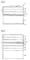
- FIG. 1 A first exemplary embodiment of a semiconductor body is shown in FIG FIG. 1 schematically shown in sectional view.
- the semiconductor body 2 has an n-type semiconductor layer 21 and a p-type semiconductor layer 22. Between the n-type semiconductor layer and the p-type semiconductor layer, an active region 20 is provided, which is provided for generating radiation.
- the layer sequence as in connection with the FIG. 1
- it is a polarity-inverted structure as described above, that is, in the growth direction, the sequence is as follows: p-type layer 22, active area 20, n-type layer 21.
- the growth direction is preferable parallel to the crystallographic C-axis of the semiconductor body.
- This layer sequence exploits the polarity of the piezoelectric fields that form in the semiconductor body 10 in order to support the trapping of charge carriers in the active region 20.
- the piezoelectric fields thus contribute to an improved capture of charge carriers in the active region 20 in this sequence.
- the internal quantum efficiency of multiple quantum wells, for example active region 20 thereby becomes almost independent of the current density.
- the semiconductor layers of the semiconductor body 2 are preferably epitaxially deposited on a growth substrate 50, such as by MOVPE or MBE.
- the semiconductor body 2 is based on a nitride compound semiconductor material and may be provided, for example, for generating ultraviolet, blue or green radiation.
- a growth substrate for example, sapphire, silicon carbide, gallium nitride, silicon, a transparent oxide, such as ZnO, or glass is suitable.
- the p-type semiconductor layer 22 contains magnesium as the p-type dopant.
- the n-type semiconductor layer 21 includes an n-type impurity such as silicon.
- the n-type semiconductor layer 21 contains a further dopant.
- magnesium is particularly suitable as a further dopant for the n-type semiconductor layer.
- the permeability of the n-type semiconductor layer 21 is increased for hydrogen.
- the further dopant may thus correspond to the p-type dopant of the p-type semiconductor layer.
- the hydrogen incorporated in the semiconductor layer 220 can thus pass through the n-conducting semiconductor layer 21 in a simplified manner and escape from the semiconductor body 2.
- the degree of activation of the p-type semiconductor layer 22 can thus be improved in a simple and reproducible manner.
- the concentration of the further dopant in the n-type semiconductor layer 21 is preferably at least 1 ⁇ 10 16 cm -3 , more preferably between 1 ⁇ 10 17 cm -3 and including 5 ⁇ 10 18 cm -3 , most preferably 1 ⁇ 10 17 cm -3 and 2 x 10 18 cm -3 .
- a good permeability to hydrogen can be achieved while maintaining good optical quality of the n-type semiconductor layer.
- the concentration of the further dopant is preferably at most 50%. Excessive compensation of the n-type dopant by the further dopant can thus be avoided.
- the p-type semiconductor layer 22 is disposed between the growth substrate 50 and the n-type semiconductor layer 21.
- the n-type semiconductor layer covers the p-type semiconductor layer 22 on the side facing away from the growth substrate 50.
- the p-type semiconductor layer is thus realized as a buried semiconductor layer which has been deposited in front of the active region 20 and in front of the n-type semiconductor layer.
- the semiconductor body can be embodied such that charge carriers are injected into the active region in a simplified manner and furthermore the piezoelectric fields occurring promote the recombination of charge carriers in the active region can.
- the p-type semiconductor layer can have a high degree of activation, so that a semiconductor chip with such a semiconductor body can have improved optoelectronic properties.
- FIG. 2 An exemplary embodiment of a semiconductor chip is shown in FIG FIG. 2 schematically shown in sectional view.
- the semiconductor chip 1 has a semiconductor body 2.
- the semiconductor body may in particular be as related to FIG. 1 be executed described.
- the semiconductor body 2 is arranged on a carrier 5, which is different from the growth substrate for the semiconductor layer sequence of the semiconductor body 2.
- the semiconductor body 2 is mechanically stable connected to the carrier 5 by means of a connecting layer 6.
- the bonding layer 6 may be, for example, a solder layer or an electrically conductive adhesive layer.
- the semiconductor chip 1 has a first contact 71 and a second contact 72.
- the contacts are provided for external electrical contacting of the semiconductor chip 1 and arranged such that charge carriers can be injected from different sides into the active region 20 during operation of the semiconductor chip and recombine there with the emission of radiation.
- a current spreading layer may be formed between the p-type semiconductor layer 22 and the second contact 72 (not explicitly shown in the figure). As a result, a current injection that is uniform in the lateral direction over the p-conducting semiconductor layer into the active region 20 can be achieved in a simplified manner.
- the current spreading layer expediently extends beyond the second contact in a lateral direction.
- the current spreading layer completely or substantially completely covers the p-type semiconductor layer 22.
- the current spreading layer may be formed as another n-type semiconductor layer and further preferably has a higher lateral conductivity than the p-type semiconductor layer.
- the further n-type semiconductor layer is preferably embodied such that a tunnel junction forms between this further n-type semiconductor layer and the p-type semiconductor layer, via which the charge carriers pass from the second contact 72 into the p-type semiconductor layer during operation of the semiconductor chip can.
- the current spreading layer may be arranged outside the semiconductor body.
- Such a current spreading layer can be applied to the prefabricated semiconductor body, for example by means of vapor deposition or sputtering.
- the current spreading layer may, for example, contain or consist of a TCO (transparent conductive oxide) material, such as ITO (indium tin oxide) or ZnO.
- TCO transparent conductive oxide
- ITO indium tin oxide
- ZnO transparent conductive oxide
- a metallic current spreading layer which is so thin that it is transparent or at least translucent for radiation generated in the active region, is also conceivable.
- the current spreading layer may also have a multilayer structure and, for example, have a TCO layer and a metal layer.
- a mirror layer 8 is formed between the semiconductor body 2 and the carrier 5.
- the radiation generated in the active region 20 and emitted in the direction of the carrier 5 can be reflected at the mirror layer. The risk of absorption of the radiation in the carrier can thus be avoided.
- the mirror layer 8 may contain, for example, a metal, such as silver, aluminum, rhodium or palladium or consist of such a material.
- the carrier 5 is preferably designed to be electrically conductive.
- the carrier 5 may contain a semiconductor material, such as germanium, gallium arsenide or silicon or consist of such a material. Deviating from the carrier 5 may also contain a ceramic, such as aluminum nitride or boron nitride, or consist of such a material.
- the semiconductor chip 1 is only exemplified as a thin-film LED chip executed.
- the growth substrate for the semiconductor body 2 can also remain in the semiconductor chip.
- the growth substrate may be thinned in regions or over the entire surface or removed in regions.
- the contacts 71, 72 may also be arranged on the same side of the semiconductor chip, so that the Semiconductor chip from only one side externally electrically contacted.
- the contacts 71, 72 are expediently designed to be electrically conductive and further preferably contain a metal, such as titanium, platinum, nickel, gold, aluminum, rhodium or palladium or a metallic alloy with at least one of the said metals.
- a metal such as titanium, platinum, nickel, gold, aluminum, rhodium or palladium or a metallic alloy with at least one of the said metals.
- FIG. 3 A second exemplary embodiment of a semiconductor body is shown in FIG. 3 schematically shown in sectional view. This second embodiment corresponds essentially to that in connection with FIG FIG. 1 described first embodiment.
- the semiconductor body 2 has a further active region 25, a further n-conducting semiconductor layer 26 and a further p-conducting semiconductor layer 27. Between the active region 20 and the further active region 25, a first tunnel layer 23 and a second tunnel layer 24 are arranged. The first tunnel layer and the second tunnel layer form a tunnel contact, via which the active regions 20, 25 are electrically interconnected in series. As a result of the additional active region, the total radiation power that can be generated in the semiconductor body can be increased.
- the tunnel layers 23, 24 are preferably different from one another with regard to the conductivity type and furthermore preferably have a high doping concentration, particularly preferably at least 1 ⁇ 10 19 cm -3 .
- first embodiment is the p-type Semiconductor layer 22 on the growth substrate 50 opposite side of the n-type semiconductor layer 21 is arranged.
- the n-type semiconductor layer 21 in this embodiment covers the p-type semiconductor layer 27 on the side facing away from the growth substrate 50.
- the p-type semiconductor layer is thus deposited on the growth substrate after the n-type semiconductor layer 21.
- the further p-type semiconductor layer 27 may be formed substantially like the p-type semiconductor layer 22 here. When the p-type semiconductor layers 22 are activated, they are exposed, so that hydrogen can escape from this semiconductor layer unhindered.
- the further p-type semiconductor layer 27 is covered by the n-type semiconductor layer 21 on the side facing away from the carrier 50. Due to the further dopant formed in the n-type semiconductor layer 21, this n-type semiconductor layer has an increased permeability to hydrogen, so that upon activation of the further p-type semiconductor layer 27, hydrogen can pass through the n-type semiconductor layer 21.
- FIGS. 4A and 4B An exemplary embodiment of a method for producing a semiconductor body can be found in FIGS FIGS. 4A and 4B schematically represented by intermediate steps. The method is described by way of example with reference to the production of a semiconductor body, as described in connection with FIG FIG. 1 is described described.
- a semiconductor layer 220 is deposited, which contains a p-type dopant and hydrogen.
- an active region 20 and an n-type semiconductor layer 21 are deposited.
- the semiconductor layer, the active region 20 and the n-type semiconductor layer 21 form the semiconductor body 2.
- the semiconductor layer 220 is activated. This can be done, for example, thermally.
- activating can, as in FIG. 4B schematically represented by arrows, hydrogen diffuse from the semiconductor layer through the active region and the n-type semiconductor layer 21 therethrough. The hydrogen can therefore be expelled from the semiconductor body 2 on the side facing away from the growth substrate.
Landscapes
- Led Devices (AREA)
- Crystals, And After-Treatments Of Crystals (AREA)
- Manufacturing Of Electric Cables (AREA)
- Photovoltaic Devices (AREA)
- Light Receiving Elements (AREA)
Applications Claiming Priority (2)
| Application Number | Priority Date | Filing Date | Title |
|---|---|---|---|
| DE102008028345A DE102008028345A1 (de) | 2008-06-13 | 2008-06-13 | Halbleiterkörper und Verfahren zur Herstellung eines Halbleiterkörpers |
| PCT/DE2009/000756 WO2009149687A1 (de) | 2008-06-13 | 2009-05-28 | Halbleiterkörper und verfahren zur herstellung eines halbleiterkörpers |
Publications (2)
| Publication Number | Publication Date |
|---|---|
| EP2286469A1 EP2286469A1 (de) | 2011-02-23 |
| EP2286469B1 true EP2286469B1 (de) | 2012-01-04 |
Family
ID=41131617
Family Applications (1)
| Application Number | Title | Priority Date | Filing Date |
|---|---|---|---|
| EP09761309A Active EP2286469B1 (de) | 2008-06-13 | 2009-05-28 | Halbleiterkörper und verfahren zur herstellung eines halbleiterkörpers |
Country Status (9)
| Country | Link |
|---|---|
| US (1) | US8581264B2 (enExample) |
| EP (1) | EP2286469B1 (enExample) |
| JP (1) | JP5661614B2 (enExample) |
| KR (1) | KR101642524B1 (enExample) |
| CN (1) | CN101971372B (enExample) |
| AT (1) | ATE540432T1 (enExample) |
| DE (1) | DE102008028345A1 (enExample) |
| TW (1) | TWI396305B (enExample) |
| WO (1) | WO2009149687A1 (enExample) |
Families Citing this family (4)
| Publication number | Priority date | Publication date | Assignee | Title |
|---|---|---|---|---|
| TWI466343B (zh) * | 2012-01-06 | 2014-12-21 | 華夏光股份有限公司 | 發光二極體裝置 |
| DE102013104192A1 (de) * | 2013-04-25 | 2014-10-30 | Osram Opto Semiconductors Gmbh | Halbleiterbauelement mit einer Zwischenschicht |
| CN113078243B (zh) * | 2016-05-20 | 2024-05-28 | 亮锐控股有限公司 | 用于生长发光器件中的层的方法 |
| KR101931798B1 (ko) * | 2017-09-19 | 2018-12-21 | 주식회사 썬다이오드코리아 | 다중 터널 정션 구조를 가지는 발광 다이오드 |
Family Cites Families (23)
| Publication number | Priority date | Publication date | Assignee | Title |
|---|---|---|---|---|
| US97269A (en) * | 1869-11-30 | Harrison berdan and john bantly | ||
| US187568A (en) * | 1877-02-20 | Improvement in harness-saddle pads | ||
| US104399A (en) * | 1870-06-21 | Improvement in cultivators | ||
| US90900A (en) * | 1869-06-01 | Improved wooden shoe | ||
| US197104A (en) * | 1877-11-13 | Improvement in trusses | ||
| US203407A (en) * | 1878-05-07 | Improvement in piano-forte actions | ||
| US58465A (en) * | 1866-10-02 | Improvement in carriage-shackles | ||
| JPH10242586A (ja) | 1997-02-24 | 1998-09-11 | Fuji Electric Co Ltd | Iii 族窒化物半導体装置およびその製造方法 |
| JP3916361B2 (ja) | 2000-02-18 | 2007-05-16 | 独立行政法人科学技術振興機構 | 低抵抗p型単結晶ZnS薄膜およびその製造方法 |
| US20020157596A1 (en) | 2001-04-30 | 2002-10-31 | Stockman Stephen A. | Forming low resistivity p-type gallium nitride |
| US6537838B2 (en) * | 2001-06-11 | 2003-03-25 | Limileds Lighting, U.S., Llc | Forming semiconductor structures including activated acceptors in buried p-type III-V layers |
| JP4233268B2 (ja) | 2002-04-23 | 2009-03-04 | シャープ株式会社 | 窒化物系半導体発光素子およびその製造方法 |
| JP2004134750A (ja) * | 2002-09-19 | 2004-04-30 | Toyoda Gosei Co Ltd | p型III族窒化物系化合物半導体の製造方法 |
| TW561637B (en) | 2002-10-16 | 2003-11-11 | Epistar Corp | LED having contact layer with dual dopant state |
| KR20050093319A (ko) * | 2004-03-18 | 2005-09-23 | 삼성전기주식회사 | 발광효율이 개선된 질화물 반도체 발광소자 및 그 제조방법 |
| US7061026B2 (en) * | 2004-04-16 | 2006-06-13 | Arima Optoelectronics Corp. | High brightness gallium nitride-based light emitting diode with transparent conducting oxide spreading layer |
| US7095052B2 (en) * | 2004-10-22 | 2006-08-22 | Avago Technologies Ecbu Ip (Singapore) Pte. Ltd. | Method and structure for improved LED light output |
| US7720124B2 (en) * | 2005-03-03 | 2010-05-18 | Panasonic Corporation | Semiconductor device and fabrication method thereof |
| DE102005035722B9 (de) | 2005-07-29 | 2021-11-18 | OSRAM Opto Semiconductors Gesellschaft mit beschränkter Haftung | Optoelektronischer Halbleiterchip und Verfahren zu dessen Herstellung |
| TWI277226B (en) * | 2005-10-24 | 2007-03-21 | Formosa Epitaxy Inc | Light emitting diode |
| DE102007018307A1 (de) | 2007-01-26 | 2008-07-31 | Osram Opto Semiconductors Gmbh | Halbleiterchip und Verfahren zur Herstellung eines Halbleiterchips |
| DE102007019079A1 (de) * | 2007-01-26 | 2008-07-31 | Osram Opto Semiconductors Gmbh | Verfahren zum Herstellen eines optoelektronischen Halbleiterchips und optoelektronischer Halbleiterchip |
| US7759670B2 (en) * | 2007-06-12 | 2010-07-20 | SemiLEDs Optoelectronics Co., Ltd. | Vertical LED with current guiding structure |
-
2008
- 2008-06-13 DE DE102008028345A patent/DE102008028345A1/de not_active Withdrawn
-
2009
- 2009-05-28 EP EP09761309A patent/EP2286469B1/de active Active
- 2009-05-28 AT AT09761309T patent/ATE540432T1/de active
- 2009-05-28 US US12/922,864 patent/US8581264B2/en active Active
- 2009-05-28 CN CN2009801090568A patent/CN101971372B/zh active Active
- 2009-05-28 WO PCT/DE2009/000756 patent/WO2009149687A1/de not_active Ceased
- 2009-05-28 JP JP2011512826A patent/JP5661614B2/ja not_active Expired - Fee Related
- 2009-05-28 KR KR1020107020378A patent/KR101642524B1/ko active Active
- 2009-06-11 TW TW098119476A patent/TWI396305B/zh not_active IP Right Cessation
Also Published As
| Publication number | Publication date |
|---|---|
| US8581264B2 (en) | 2013-11-12 |
| US20110073902A1 (en) | 2011-03-31 |
| JP2011523219A (ja) | 2011-08-04 |
| EP2286469A1 (de) | 2011-02-23 |
| KR20110015510A (ko) | 2011-02-16 |
| ATE540432T1 (de) | 2012-01-15 |
| CN101971372B (zh) | 2013-05-15 |
| TW201019508A (en) | 2010-05-16 |
| DE102008028345A1 (de) | 2009-12-17 |
| JP5661614B2 (ja) | 2015-01-28 |
| KR101642524B1 (ko) | 2016-07-25 |
| WO2009149687A1 (de) | 2009-12-17 |
| CN101971372A (zh) | 2011-02-09 |
| TWI396305B (zh) | 2013-05-11 |
Similar Documents
| Publication | Publication Date | Title |
|---|---|---|
| EP2274774B1 (de) | Strahlungsemittierender halbleiterchip | |
| DE102009060747B4 (de) | Halbleiterchip | |
| DE102007032555A1 (de) | Halbleiterchip und Verfahren zur Herstellung eines Halbleiterchips | |
| EP1906460A2 (de) | Halbleiterkörper und Halbleiterchip mit einem Halbleiterkörper | |
| DE102008021403A1 (de) | Optoelektronischer Halbleiterkörper und Verfahren zu dessen Herstellung | |
| DE112018000553B4 (de) | Optoelektronischer Halbleiterchip | |
| EP2599131A1 (de) | Strahlungsemittierender halbleiterchip und verfahren zur herstellung eines strahlungsemittierenden halbleiterchips | |
| EP3120391A1 (de) | Photoaktives halbleiterbauelement sowie verfahren zum herstellen eines photoaktiven halbleiterbauelementes | |
| EP2286469B1 (de) | Halbleiterkörper und verfahren zur herstellung eines halbleiterkörpers | |
| EP2111650B1 (de) | Halbleiterchip und verfahren zur herstellung eines halbleiterchips | |
| EP1658643B1 (de) | Strahlungemittierendes halbleiterbauelement | |
| DE102006035627A1 (de) | LED-Halbleiterkörper | |
| EP2338182B1 (de) | Optoelektronisches halbleiterbauelement | |
| EP1929552B1 (de) | Optoelektronisches halbleiterbauelement mit stromaufweitungsschicht | |
| DE102016113274B4 (de) | Optoelektronischer Halbleiterchip | |
| DE10346605A1 (de) | Strahlungemittierendes Halbleiterbauelement | |
| DE102011115299B4 (de) | Optoelektronischer Halbleiterchip und Verfahren zur Herstellung eines optoelektronischen Halbleiterchips | |
| DE102004061865A1 (de) | Verfahren zur Herstellung eines Dünnfilmhalbleiterchips | |
| WO2015176873A1 (de) | Verfahren zur herstellung eines optoelektronischen halbleiterchips und optoelektronischer halbleiterchip | |
| DE102012106998A1 (de) | Reflektierendes Kontaktschichtsystem für ein optoelektronisches Bauelement und Verfahren zu dessen Herstellung | |
| WO2019072520A1 (de) | Verfahren zur herstellung eines optoelektronischen halbleiterchips und optoelektronischer halbleiterchip | |
| WO2019042746A1 (de) | Optoelektronisches halbleiterbauelement |
Legal Events
| Date | Code | Title | Description |
|---|---|---|---|
| PUAI | Public reference made under article 153(3) epc to a published international application that has entered the european phase |
Free format text: ORIGINAL CODE: 0009012 |
|
| 17P | Request for examination filed |
Effective date: 20100906 |
|
| AK | Designated contracting states |
Kind code of ref document: A1 Designated state(s): AT BE BG CH CY CZ DE DK EE ES FI FR GB GR HR HU IE IS IT LI LT LU LV MC MK MT NL NO PL PT RO SE SI SK TR |
|
| AX | Request for extension of the european patent |
Extension state: AL BA RS |
|
| RIN1 | Information on inventor provided before grant (corrected) |
Inventor name: FLOETER, RICHARD Inventor name: GROLIER, VINCENT Inventor name: STRASSBURG, MARTIN Inventor name: LUGAUER, HANS-JUERGEN Inventor name: HAHN, BERTHOLD |
|
| GRAP | Despatch of communication of intention to grant a patent |
Free format text: ORIGINAL CODE: EPIDOSNIGR1 |
|
| DAX | Request for extension of the european patent (deleted) | ||
| GRAS | Grant fee paid |
Free format text: ORIGINAL CODE: EPIDOSNIGR3 |
|
| GRAA | (expected) grant |
Free format text: ORIGINAL CODE: 0009210 |
|
| AK | Designated contracting states |
Kind code of ref document: B1 Designated state(s): AT BE BG CH CY CZ DE DK EE ES FI FR GB GR HR HU IE IS IT LI LT LU LV MC MK MT NL NO PL PT RO SE SI SK TR |
|
| REG | Reference to a national code |
Ref country code: GB Ref legal event code: FG4D Free format text: NOT ENGLISH |
|
| REG | Reference to a national code |
Ref country code: CH Ref legal event code: EP |
|
| REG | Reference to a national code |
Ref country code: AT Ref legal event code: REF Ref document number: 540432 Country of ref document: AT Kind code of ref document: T Effective date: 20120115 |
|
| REG | Reference to a national code |
Ref country code: IE Ref legal event code: FG4D |
|
| REG | Reference to a national code |
Ref country code: DE Ref legal event code: R096 Ref document number: 502009002405 Country of ref document: DE Effective date: 20120308 |
|
| REG | Reference to a national code |
Ref country code: NL Ref legal event code: VDEP Effective date: 20120104 |
|
| PG25 | Lapsed in a contracting state [announced via postgrant information from national office to epo] |
Ref country code: SI Free format text: LAPSE BECAUSE OF FAILURE TO SUBMIT A TRANSLATION OF THE DESCRIPTION OR TO PAY THE FEE WITHIN THE PRESCRIBED TIME-LIMIT Effective date: 20120104 |
|
| LTIE | Lt: invalidation of european patent or patent extension |
Effective date: 20120104 |
|
| PG25 | Lapsed in a contracting state [announced via postgrant information from national office to epo] |
Ref country code: BG Free format text: LAPSE BECAUSE OF FAILURE TO SUBMIT A TRANSLATION OF THE DESCRIPTION OR TO PAY THE FEE WITHIN THE PRESCRIBED TIME-LIMIT Effective date: 20120404 Ref country code: NL Free format text: LAPSE BECAUSE OF FAILURE TO SUBMIT A TRANSLATION OF THE DESCRIPTION OR TO PAY THE FEE WITHIN THE PRESCRIBED TIME-LIMIT Effective date: 20120104 Ref country code: HR Free format text: LAPSE BECAUSE OF FAILURE TO SUBMIT A TRANSLATION OF THE DESCRIPTION OR TO PAY THE FEE WITHIN THE PRESCRIBED TIME-LIMIT Effective date: 20120104 Ref country code: LT Free format text: LAPSE BECAUSE OF FAILURE TO SUBMIT A TRANSLATION OF THE DESCRIPTION OR TO PAY THE FEE WITHIN THE PRESCRIBED TIME-LIMIT Effective date: 20120104 Ref country code: NO Free format text: LAPSE BECAUSE OF FAILURE TO SUBMIT A TRANSLATION OF THE DESCRIPTION OR TO PAY THE FEE WITHIN THE PRESCRIBED TIME-LIMIT Effective date: 20120404 Ref country code: IS Free format text: LAPSE BECAUSE OF FAILURE TO SUBMIT A TRANSLATION OF THE DESCRIPTION OR TO PAY THE FEE WITHIN THE PRESCRIBED TIME-LIMIT Effective date: 20120504 |
|
| REG | Reference to a national code |
Ref country code: IE Ref legal event code: FD4D |
|
| PG25 | Lapsed in a contracting state [announced via postgrant information from national office to epo] |
Ref country code: GR Free format text: LAPSE BECAUSE OF FAILURE TO SUBMIT A TRANSLATION OF THE DESCRIPTION OR TO PAY THE FEE WITHIN THE PRESCRIBED TIME-LIMIT Effective date: 20120405 Ref country code: FI Free format text: LAPSE BECAUSE OF FAILURE TO SUBMIT A TRANSLATION OF THE DESCRIPTION OR TO PAY THE FEE WITHIN THE PRESCRIBED TIME-LIMIT Effective date: 20120104 Ref country code: PT Free format text: LAPSE BECAUSE OF FAILURE TO SUBMIT A TRANSLATION OF THE DESCRIPTION OR TO PAY THE FEE WITHIN THE PRESCRIBED TIME-LIMIT Effective date: 20120504 Ref country code: PL Free format text: LAPSE BECAUSE OF FAILURE TO SUBMIT A TRANSLATION OF THE DESCRIPTION OR TO PAY THE FEE WITHIN THE PRESCRIBED TIME-LIMIT Effective date: 20120104 Ref country code: LV Free format text: LAPSE BECAUSE OF FAILURE TO SUBMIT A TRANSLATION OF THE DESCRIPTION OR TO PAY THE FEE WITHIN THE PRESCRIBED TIME-LIMIT Effective date: 20120104 |
|
| PG25 | Lapsed in a contracting state [announced via postgrant information from national office to epo] |
Ref country code: CY Free format text: LAPSE BECAUSE OF FAILURE TO SUBMIT A TRANSLATION OF THE DESCRIPTION OR TO PAY THE FEE WITHIN THE PRESCRIBED TIME-LIMIT Effective date: 20120104 |
|
| PG25 | Lapsed in a contracting state [announced via postgrant information from national office to epo] |
Ref country code: IE Free format text: LAPSE BECAUSE OF FAILURE TO SUBMIT A TRANSLATION OF THE DESCRIPTION OR TO PAY THE FEE WITHIN THE PRESCRIBED TIME-LIMIT Effective date: 20120104 Ref country code: EE Free format text: LAPSE BECAUSE OF FAILURE TO SUBMIT A TRANSLATION OF THE DESCRIPTION OR TO PAY THE FEE WITHIN THE PRESCRIBED TIME-LIMIT Effective date: 20120104 Ref country code: DK Free format text: LAPSE BECAUSE OF FAILURE TO SUBMIT A TRANSLATION OF THE DESCRIPTION OR TO PAY THE FEE WITHIN THE PRESCRIBED TIME-LIMIT Effective date: 20120104 Ref country code: RO Free format text: LAPSE BECAUSE OF FAILURE TO SUBMIT A TRANSLATION OF THE DESCRIPTION OR TO PAY THE FEE WITHIN THE PRESCRIBED TIME-LIMIT Effective date: 20120104 Ref country code: SE Free format text: LAPSE BECAUSE OF FAILURE TO SUBMIT A TRANSLATION OF THE DESCRIPTION OR TO PAY THE FEE WITHIN THE PRESCRIBED TIME-LIMIT Effective date: 20120104 Ref country code: CZ Free format text: LAPSE BECAUSE OF FAILURE TO SUBMIT A TRANSLATION OF THE DESCRIPTION OR TO PAY THE FEE WITHIN THE PRESCRIBED TIME-LIMIT Effective date: 20120104 |
|
| PLBE | No opposition filed within time limit |
Free format text: ORIGINAL CODE: 0009261 |
|
| STAA | Information on the status of an ep patent application or granted ep patent |
Free format text: STATUS: NO OPPOSITION FILED WITHIN TIME LIMIT |
|
| BERE | Be: lapsed |
Owner name: OSRAM OPTO SEMICONDUCTORS G.M.B.H. Effective date: 20120531 |
|
| PG25 | Lapsed in a contracting state [announced via postgrant information from national office to epo] |
Ref country code: IT Free format text: LAPSE BECAUSE OF FAILURE TO SUBMIT A TRANSLATION OF THE DESCRIPTION OR TO PAY THE FEE WITHIN THE PRESCRIBED TIME-LIMIT Effective date: 20120104 Ref country code: SK Free format text: LAPSE BECAUSE OF FAILURE TO SUBMIT A TRANSLATION OF THE DESCRIPTION OR TO PAY THE FEE WITHIN THE PRESCRIBED TIME-LIMIT Effective date: 20120104 |
|
| 26N | No opposition filed |
Effective date: 20121005 |
|
| PG25 | Lapsed in a contracting state [announced via postgrant information from national office to epo] |
Ref country code: MC Free format text: LAPSE BECAUSE OF NON-PAYMENT OF DUE FEES Effective date: 20120531 |
|
| REG | Reference to a national code |
Ref country code: DE Ref legal event code: R097 Ref document number: 502009002405 Country of ref document: DE Effective date: 20121005 |
|
| PG25 | Lapsed in a contracting state [announced via postgrant information from national office to epo] |
Ref country code: MK Free format text: LAPSE BECAUSE OF FAILURE TO SUBMIT A TRANSLATION OF THE DESCRIPTION OR TO PAY THE FEE WITHIN THE PRESCRIBED TIME-LIMIT Effective date: 20120104 Ref country code: BE Free format text: LAPSE BECAUSE OF NON-PAYMENT OF DUE FEES Effective date: 20120531 |
|
| PG25 | Lapsed in a contracting state [announced via postgrant information from national office to epo] |
Ref country code: ES Free format text: LAPSE BECAUSE OF FAILURE TO SUBMIT A TRANSLATION OF THE DESCRIPTION OR TO PAY THE FEE WITHIN THE PRESCRIBED TIME-LIMIT Effective date: 20120415 |
|
| PG25 | Lapsed in a contracting state [announced via postgrant information from national office to epo] |
Ref country code: MT Free format text: LAPSE BECAUSE OF FAILURE TO SUBMIT A TRANSLATION OF THE DESCRIPTION OR TO PAY THE FEE WITHIN THE PRESCRIBED TIME-LIMIT Effective date: 20120104 |
|
| REG | Reference to a national code |
Ref country code: CH Ref legal event code: PL |
|
| PG25 | Lapsed in a contracting state [announced via postgrant information from national office to epo] |
Ref country code: LI Free format text: LAPSE BECAUSE OF NON-PAYMENT OF DUE FEES Effective date: 20130531 Ref country code: CH Free format text: LAPSE BECAUSE OF NON-PAYMENT OF DUE FEES Effective date: 20130531 |
|
| PG25 | Lapsed in a contracting state [announced via postgrant information from national office to epo] |
Ref country code: TR Free format text: LAPSE BECAUSE OF FAILURE TO SUBMIT A TRANSLATION OF THE DESCRIPTION OR TO PAY THE FEE WITHIN THE PRESCRIBED TIME-LIMIT Effective date: 20120104 |
|
| PG25 | Lapsed in a contracting state [announced via postgrant information from national office to epo] |
Ref country code: LU Free format text: LAPSE BECAUSE OF NON-PAYMENT OF DUE FEES Effective date: 20120528 |
|
| PG25 | Lapsed in a contracting state [announced via postgrant information from national office to epo] |
Ref country code: HU Free format text: LAPSE BECAUSE OF FAILURE TO SUBMIT A TRANSLATION OF THE DESCRIPTION OR TO PAY THE FEE WITHIN THE PRESCRIBED TIME-LIMIT Effective date: 20090528 |
|
| REG | Reference to a national code |
Ref country code: AT Ref legal event code: MM01 Ref document number: 540432 Country of ref document: AT Kind code of ref document: T Effective date: 20140528 |
|
| PG25 | Lapsed in a contracting state [announced via postgrant information from national office to epo] |
Ref country code: AT Free format text: LAPSE BECAUSE OF NON-PAYMENT OF DUE FEES Effective date: 20140528 |
|
| REG | Reference to a national code |
Ref country code: FR Ref legal event code: PLFP Year of fee payment: 8 |
|
| REG | Reference to a national code |
Ref country code: FR Ref legal event code: PLFP Year of fee payment: 9 |
|
| REG | Reference to a national code |
Ref country code: FR Ref legal event code: PLFP Year of fee payment: 10 |
|
| PGFP | Annual fee paid to national office [announced via postgrant information from national office to epo] |
Ref country code: FR Payment date: 20180522 Year of fee payment: 10 |
|
| PGFP | Annual fee paid to national office [announced via postgrant information from national office to epo] |
Ref country code: GB Payment date: 20180518 Year of fee payment: 10 |
|
| GBPC | Gb: european patent ceased through non-payment of renewal fee |
Effective date: 20190528 |
|
| PG25 | Lapsed in a contracting state [announced via postgrant information from national office to epo] |
Ref country code: GB Free format text: LAPSE BECAUSE OF NON-PAYMENT OF DUE FEES Effective date: 20190528 |
|
| PG25 | Lapsed in a contracting state [announced via postgrant information from national office to epo] |
Ref country code: FR Free format text: LAPSE BECAUSE OF NON-PAYMENT OF DUE FEES Effective date: 20190531 |
|
| P01 | Opt-out of the competence of the unified patent court (upc) registered |
Effective date: 20230825 |
|
| REG | Reference to a national code |
Ref country code: DE Ref legal event code: R079 Ref document number: 502009002405 Country of ref document: DE Free format text: PREVIOUS MAIN CLASS: H01L0033000000 Ipc: H10H0020000000 |
|
| PGFP | Annual fee paid to national office [announced via postgrant information from national office to epo] |
Ref country code: DE Payment date: 20250521 Year of fee payment: 17 |