EP2284524A2 - Mikrokalometrie für die Röntgenstrahlspektroskopie - Google Patents
Mikrokalometrie für die Röntgenstrahlspektroskopie Download PDFInfo
- Publication number
- EP2284524A2 EP2284524A2 EP10171817A EP10171817A EP2284524A2 EP 2284524 A2 EP2284524 A2 EP 2284524A2 EP 10171817 A EP10171817 A EP 10171817A EP 10171817 A EP10171817 A EP 10171817A EP 2284524 A2 EP2284524 A2 EP 2284524A2
- Authority
- EP
- European Patent Office
- Prior art keywords
- ray
- sample
- rays
- electron beam
- detectors
- Prior art date
- Legal status (The legal status is an assumption and is not a legal conclusion. Google has not performed a legal analysis and makes no representation as to the accuracy of the status listed.)
- Granted
Links
- 238000000441 X-ray spectroscopy Methods 0.000 title 1
- 238000010894 electron beam technology Methods 0.000 claims abstract 11
- 238000013507 mapping Methods 0.000 claims abstract 3
- 239000000463 material Substances 0.000 claims 10
- 238000000034 method Methods 0.000 claims 6
- 239000006096 absorbing agent Substances 0.000 claims 3
- 229910052732 germanium Inorganic materials 0.000 claims 2
- GNPVGFCGXDBREM-UHFFFAOYSA-N germanium atom Chemical compound [Ge] GNPVGFCGXDBREM-UHFFFAOYSA-N 0.000 claims 2
- 239000011521 glass Substances 0.000 claims 2
- 230000003116 impacting effect Effects 0.000 claims 2
- 238000010884 ion-beam technique Methods 0.000 claims 2
- 238000009377 nuclear transmutation Methods 0.000 claims 2
- 239000013078 crystal Substances 0.000 claims 1
- 150000002500 ions Chemical class 0.000 claims 1
- 239000004065 semiconductor Substances 0.000 claims 1
- 239000007787 solid Substances 0.000 claims 1
- 230000009977 dual effect Effects 0.000 abstract 1
Images


Classifications
-
- G—PHYSICS
- G01—MEASURING; TESTING
- G01N—INVESTIGATING OR ANALYSING MATERIALS BY DETERMINING THEIR CHEMICAL OR PHYSICAL PROPERTIES
- G01N23/00—Investigating or analysing materials by the use of wave or particle radiation, e.g. X-rays or neutrons, not covered by groups G01N3/00 – G01N17/00, G01N21/00 or G01N22/00
- G01N23/20—Investigating or analysing materials by the use of wave or particle radiation, e.g. X-rays or neutrons, not covered by groups G01N3/00 – G01N17/00, G01N21/00 or G01N22/00 by using diffraction of the radiation by the materials, e.g. for investigating crystal structure; by using scattering of the radiation by the materials, e.g. for investigating non-crystalline materials; by using reflection of the radiation by the materials
- G01N23/20008—Constructional details of analysers, e.g. characterised by X-ray source, detector or optical system; Accessories therefor; Preparing specimens therefor
- G01N23/20025—Sample holders or supports therefor
- G01N23/20033—Sample holders or supports therefor provided with temperature control or heating means
-
- H—ELECTRICITY
- H01—ELECTRIC ELEMENTS
- H01J—ELECTRIC DISCHARGE TUBES OR DISCHARGE LAMPS
- H01J37/00—Discharge tubes with provision for introducing objects or material to be exposed to the discharge, e.g. for the purpose of examination or processing thereof
- H01J37/02—Details
- H01J37/244—Detectors; Associated components or circuits therefor
-
- H—ELECTRICITY
- H01—ELECTRIC ELEMENTS
- H01J—ELECTRIC DISCHARGE TUBES OR DISCHARGE LAMPS
- H01J37/00—Discharge tubes with provision for introducing objects or material to be exposed to the discharge, e.g. for the purpose of examination or processing thereof
- H01J37/252—Tubes for spot-analysing by electron or ion beams; Microanalysers
- H01J37/256—Tubes for spot-analysing by electron or ion beams; Microanalysers using scanning beams
-
- H—ELECTRICITY
- H01—ELECTRIC ELEMENTS
- H01J—ELECTRIC DISCHARGE TUBES OR DISCHARGE LAMPS
- H01J2237/00—Discharge tubes exposing object to beam, e.g. for analysis treatment, etching, imaging
- H01J2237/244—Detection characterized by the detecting means
- H01J2237/2441—Semiconductor detectors, e.g. diodes
- H01J2237/24415—X-ray
- H01J2237/2442—Energy-dispersive (Si-Li type) spectrometer
Definitions
- the present invention relates to a system for determining the composition of a sample.
- Electron probe microanalyzers and electron microscopes having an attached x-ray spectrometer are used to determine the composition of microscopic or nanoscopic regions of a surface.
- the detectors determine the energy or wavelengths of x-rays emitted from the sample and infer the composition of material under the electron beam from the energy or wavelength of the x-rays. Because the x-rays characteristic of different materials may have energies that are only slightly different, a detector needs sufficient resolution to differentiate between closely spaced x-ray energies. To process a sample in reasonable amount of time, x-ray detectors need to be able to process a large number of x-rays each second.
- the number of x-rays that a detector can process each second is referred to as its "maximum count rate”.
- the rate at which the received x-rays are processed is referred to as the "count rate” and is typically expressed in units of counts per second (cps).
- WDS wavelength dispersive spectrometers
- EDS energy dispersive spectrometers
- a WDS can provide better spectral resolution and greater maximum count rate for a particular wavelength band of x-rays
- an EDS is better adapted to measuring x-rays of different energies from multiple elements.
- an EDS can acquire an entire spectrum in parallel, while a WDS is limited to serial acquisition.
- EDS detectors preferably process each x-ray quickly, so that each energy measurement is complete before the next x-ray is received.
- the most common type of energy dispersive x-ray spectrometer uses a semiconductor x-ray detector in which the x-rays form electron-hole pairs.
- the electron-hole pairs are detected as an electric current and the number of pairs created by each x-ray depends on the energy of the x-ray.
- EDS systems with solid state detectors typically have a high count rate, up to hundreds of thousands of counts per second, their energy resolution at approximately 6 keV is worse than about 100 eV, which makes it impossible to differentiate closely spaced x-ray peaks.
- microcalorimeter-type EDS Another type of energy dispersive x-ray spectrometer is the microcalorimeter-type EDS system, in which an x-ray is absorbed by a detector and the x-ray energy is determined by measuring an increase in temperature of the detector, the increase being proportional to the energy of the absorbed x-ray.
- the energy resolution of the microcalorimeter detector is superior to that of the semiconductor detector, less than 5 eV at an x-ray energy of approximately 6 keV in some systems, but microcalorimeter detectors typically are only capable of processing less than 500 x-rays per second.
- Microcalorimeter-type EDS systems are described, for example, in U.S. Pat. No.5,880,467 to Martinis, et al .
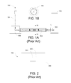
- FIG. 1A shows at typical microcalorimeter-type EDS system 100, which includes a scanning electron microscope 102 and an x-ray optic 104 that transmit x-rays emitted from a sample 106 to a detector 108 cooled by a cryostat 110.
- X-ray optics are typically either made from glass capillaries or from a thin metallic film, and are described, for example, in U.S. Pat. No. 6,094,471 to Silver et al. for "X-ray Diagnostic System," and U.S. Pat. No. 6,479,818 to McCarthy et al . for "Application of x-ray optics to energy dispersive spectroscopy.”
- FIG. 1B shows an enlarged cross section of X-ray optic 104 of FIG. 1 .
- X-ray optics used with a typical prior art microcalorimeter-type EDS has an acceptance angle of two to three degrees.
- FIG. 2 shows that detector 108 typically comprises an x-ray absorber 202 and a temperature measuring device 204 in contact with the absorber.
- the x-ray absorber 202 and temperature measuring device 204 are maintained at a very low temperature, typically below 100 mK, have a very low combined heat capacity and a weak thermal link to a low temperature heat sink 206.
- the weak thermal link enables the thermal isolation needed for a temperature rise to occur.
- the output peak height (measured by the temperature measuring device) is related to the x-ray photon energy (E) & the combined heat capacity (C) of the absorber and the temperature measuring device.
- the energy resolution of the detector is approximately proportional to (kT 2 C) 0.5 (where k is the Botzmann constant and T is temperature).
- the thermal link between the absorber and the low temperature heat sink is made weaker, the temperature of the absorber will rise further, increasing resolution.
- the weaker thermal link increases the time required to cool the absorber after the x-ray is processed, thereby reducing the maximum count rate that can be processed by the detector.
- the x-ray absorbing material is typically gold
- the temperature measuring device employed by most commercial systems includes a transition edge sensor, which includes a layer of non-superconducting material and a layer of superconducting material maintained near its transition temperature, that is, the temperature at which it stops superconducting.
- An electrical current through the transition edge sensor changes as the temperature of the sensor changes.
- the change in electrical current is typically amplified using a superconducting quantum interference device (SQUID).
- SQUID superconducting quantum interference device
- microcalorimetry over solid state detectors is superior energy resolution.
- prior art microcalorimeters have a resolution better than 15 eV, and in some cases better than 3 eV, whereas conventional EDS detectors are limited to a resolution of about 120 eV.
- microcalorimeters can resolve closely spaced characteristic x-ray lines. This is highly desirable for low voltage microanalysis, that is, microanalysis performed using an electron beam energy in the range of 1-5 keV, because:
- the low energy end of the x-ray spectrum contains a large number of closely spaced characteristic x-ray peaks; specifically, the K, L and M lines of low, medium and high atomic number elements, respectively.
- the low energy x-ray peaks overlap in conventional EDS spectra, necessitating the use of higher energy x-ray peaks which can only be excited by high energy (10-30 keV) electron beams.
- the electron penetration range and the electron-solid interaction volume are approximately proportional to E b 1.67 and (E b 1.67 ) 3 , respectively, where E b is the electron beam energy.
- E b is the electron beam energy.
- X-rays are emitted from some fraction, typically the top one to two thirds of the interaction volume, the exact fraction being a function of the material type and the energy of the x-ray photons and the electron beam.
- the surface sensitivity and spatial resolution of microanalysis are strong functions of electron beam energy. Low beam energies are needed for maximum spatial resolution and surface sensitivity.
- the main technical disadvantage of microcalorimetry over conventional EDS is low throughput, caused by two distinct phenomena.
- the solid angle over which x-rays are collected is severely limited by detector design requirements, causing the fraction of emitted x-rays collected by the detector to be very small.
- the surface area of a typical x-ray absorber is on the order of 0.1 mm 2 and detector placement close to the sample is inhibited by the bulky nature of the hardware needed to cool the detector to below 100 mK.
- solid state EDS detectors have surface areas in the range of 10 to 80 mm 2 , and the detectors can be placed within a few centimeters of the sample.
- the second phenomenon that limits the throughput of microcalorimeter x-ray detectors is that the maximum count rate of a single detector is thermodynamically limited to less than approximately 500 cps.
- the maximum count rates of conventional, solid state EDS (Si(Li) and silicon drift) detectors are on the order of 10 4 to 10 5 cps.
- microcalorimeter-type EDS systems would require the use of a very high electron beam current to collect sufficient x-rays to form a useful x-ray map in a reasonable time period.
- a high electron beam current however impedes electron beam focusing (due to the dependence of electron optical aberrations on beam current), causes rapid damage of electron sensitive samples, gives rise to rapid contamination buildup rates, and gives rise to severe charging of electrical insulators.
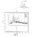
- FIG. 3 shows portions of an x-ray spectrum of the mineral monazite drawn at three different scales.
- Enlarged graph 303 shows the large number of peaks available to characterize the sample in the low energy range. While the resolution is sufficiently high to differentiate a large number of closely spaced peaks, it took more than 11 hours to collect enough x-rays to analyze a single point on the sample.
- Increased beam current increases the size of the electron beam, reducing the spatial resolution of the material analysis at low electron beam energies.
- the count rate of the microcalorimeter detector is limited.
- the thermal path between the absorber and the cold substrate is sufficiently weak to provide a high amplitude temperature pulse upon absorption of an x-ray, the absorber takes longer to cool back down after a pulse is detected, reducing the count rate.
- a more thermally conductive path between the x-ray absorber and the cold sink substrate would allow more pulses per second to be counted, but would reduce the temperature change, and therefore the measurement accuracy of the x-ray energy.
- the industry needs an EDS system capable x-ray mapping at high spatial resolution and high energy resolution.
- An object of the invention is to provide an EDS microcalorimeter system with the capability of performing high resolution mapping.
- the present invention includes a microcalorimeter-type EDS system that provides sufficient resolution and throughput for practical high spatial resolution x-ray mapping of a sample.
- Some embodiments of the invention use a wide-angle opening for x-ray optics to increase the fraction of x-rays leaving the sample that impinge on the detector.
- Some embodiments of the invention use multiple detectors to improve the maximum count rate that can be processed by the EDS system.
- Some embodiments of the invention use a neutron transmutation doped temperature measurement element to improve resolution.
- Some embodiments use a tin x-ray absorber.
- Some embodiments of the invention use a JFET amplifier to measure the change in current of the temperature-sensing element.
- Some embodiments of the invention include a dual beam system that provides an electron beam and an ion beam.
- the electron beam can be used to generate x-rays for analysis and the ion beam can be used to expose underlying material to analyze.
- the ion beam can be used to expose underlying material to analyze.
- a three-dimensional map of material present on the sample can be created.
- Some embodiments use rapid electron beam scanning and periodic plasma cleaning to enable drift correction, and minimization of sample damage, contamination buildup and charging; that is problems the severity of which increases with improved spatial resolution.
- FIG. 1 shows a typical prior art microcalorimeter-type energy dispersive x-ray spectrometer.
- FIG. 1B shows an enlarged cross section of the X-ray optic shown in FIG. 1A ;
- FIG. 2 shows a prior art detector used with the system of FIG. 1A ;
- FIG. 3 shows portions of an x-ray spectrum drawn at three different scales of the mineral monazite
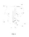
- FIG. 4 shows a preferred embodiment of a microcalorimeter-type EDS system of the present invention
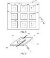
- FIG. 5 shows an array of x-ray detectors
- FIG. 6 shows an individual x-ray detector
- FIG. 7 shows a typical output pulse from a detector of FIG. 6
- FIG. 8 shows the figure of merit for a number of characteristic x-ray peaks excited in single element materials by a 5 keV electron beam.
- FIG. 9 shows an x-ray spectrum, with portions of the spectrum shown in enlarged views.
- Preferred embodiments of the present invention provide an improved microcalorimeter-type EDS system.
- Various embodiments of the system provide improved throughput, reliability, stability, and energy resolution.
- a preferred method or apparatus of the present invention has many novel aspects, and because the invention can be embodied in different methods or apparatuses for different purposes, not every aspect need be present in every embodiment. Many the aspects of the described embodiments may be separately patentable.
- a preferred embodiment of the invention comprises an x-ray microcalorimeter together with a dual beam system configured so as to enable high-resolution two-dimensional or three-dimensional x-ray mapping.
- FIG. 4 shows a preferred embodiment of the present invention.
- a microcalorimeter-type EDS system 400 includes a vacuum chamber 401 for maintaining a sample 402 on a sample XYZ stage 403, electron beam column 404 and an ion beam column 405.
- Electron beam column 404 includes a high brightness electron source, such as a Schottky emitter or cold field emitter, and ion column 405 is preferably includes a liquid metal ion source or a high brightness plasma source.
- a laser beam could be provided in place of or in addition to the focused ion beam system for removing material from the surface.
- the vacuum chamber could be a high vacuum chamber or the higher pressure vacuum chamber of an environmental scanning electron microscope.
- the system also preferably includes a plasma generator 406 for generating a plasma to remove contamination, such as carbon deposition, from the sample 402 before and during processing.
- a computer 408 controls the operation of the parts of system 400.
- a computer memory 409 stores a program for operating system 400 in accordance with the methods of the present invention.
- An x-ray optic 410 has a large acceptance angle, preferably greater than 10 degrees, more preferably greater than 15 degrees, and most preferably about 20 degrees or greater.
- the acceptance angle is the greatest angle at which a ray entering the opening will be transmitted through the optic. That is, a ray entering the optic parallel to an axis of the optic will be transmitted, but a ray entering the optic at a sharp angle to the axis will not be transmitted.
- X-ray optic 410 is preferably of the glass capillary bundle type.
- X-ray optic 410 preferably includes a point-to-parallel collimating lens 412 and then a parallel-to-point focusing lens 414 to transfers the x-rays from the vacuum chamber to detector assembly 420, which may include multiple individual detectors.
- the x-ray focusing optic can alternatively be comprised of a single point-to-point glass capillary focusing lens.
- a point-to-point focusing optic receives x-rays emanating from a point on the surface and focuses those x-rays to a point on the detector.
- Point-to-parallel-parallel-to-point optics receive x-rays from a point on the sample, collimate the x-rays so that they are moving parallel to each other for a distance, and then the parallel rays are converged back to a point.
- Point-to-parallel and parallel-to-point optical elements allow the x-rays to be routed over a range of distances between the sample to the detector simply by changing the distance between the elements 412 and 414, but the additional optical element also reduces the efficiency of the transfer.
- the glass capillary bundle is similar to the one specified in U.S. Pat. No. 6,094,471 to Silver et al. , but with an increased acceptance angle.
- Such x-ray optics are available commercially, for example, from X-Ray Optical Systems, Inc., East Greenbush, New York.
- the increased entrance angle allows the optic to receive x-rays from a larger solid angle from the sample.
- a gold foil-type optic can also be used, to reduce cost.
- the x-ray optic typically functions as a low pass filter and can be tuned to maximize the transmission of low energy x-rays, and to reject undesired higher energy x-rays.
- the x-ray optic preferably has a focal length of between 10 mm and 1000 mm, for example, 470 mm, and rejects x-rays above an energy of approximately 2.3 keV.
- the focal length is the distance from the sample to the x-ray optic.
- the rear focal length is the focal length from the optic to the focal plane that typically contains the detector that receives the x-rays.
- the front and rear focal lengths may be equal or different.
- the microcalorimeter preferably provides a large solid angle of collection, that is, a solid collection angle greater than 10 -3 sr, more preferably greater than 10 -2 sr, and most preferably greater than 10 -1 sr.
- the large solid angle can be achieved, for example, through the use of a high efficiency x-ray focusing optic or by detector placement in close proximity to the sample. The large solid angle allows more of the x-rays generated at the sample to be routed to the detector.
- Detector assembly 420 preferably includes multiple individual detectors cooled by a single cryostat.
- FIG. 5 shows a preferred detector assembly 420 comprises an array 502 that preferably includes at least nine individual detectors 504, all cooled by a single cryostat 506.
- Each includes an x-ray absorber 507 and a temperature sensor 508 between the absorber 507 and the cryostat 506, with the temperature sensor connected to the cold sink by the leads as in FIG. 6 below.
- Multiple individual detectors increase the count rate of the detector assembly by preventing pulse pileup artifacts.
- the x-rays from the sample are spread over multiple detectors, so that while one detector is temporarily unavailable due to its detecting a first pulse, other detectors can be detecting other incoming x-rays.
- each individual detector can be designed for higher resolution without reducing the overall ability of the system to process incoming x-rays. That is, the thermal connection between the absorber and the cold sink can be weaker so that the signal from each pulse is greater, thereby providing higher energy resolution while reducing the maximum count rate requirement of the individual detector.
- the x-ray flux is preferably the same at each of the multiple detectors comprising the detector array 502.
- the constant flux profile may be achieved by positioning the x-ray detector array 502 in the focal plane of x-ray optic 410, or x-ray detector array 502 may be positioned away from the focal plane so that the x-ray flux is decreased and the x-ray image expanded over the array.
- FIG. 6 shows a preferred individual x-ray detector 504 that comprises a tin absorber 604 maintained at about 60 mK and a temperature measuring device 608, which is in thermal contact but electrically isolated from absorber 604.
- the absorber 604 is preferably about 200 x 200 microns in area and about 10 microns thick.
- Temperature measuring device 608 preferably is preferably a germanium semiconductor, doped with Se, Ga and As by neutron transmutation doping. Neutron transmutation doping provides a very uniform doping profile with a dopant concentration greater than 10 16 cm -2 .
- Leads 610 provide electrical and thermal links from the temperature sensor 606 to a pre-amplifier and a cold bath.
- the leads 610 from the multiple x-ray detectors are in contact with cryostat 506 to cool the absorbers back to operating temperature after detecting a pulse and warming.
- the thermal conductance between the tin absorber and the cold sink is preferably sufficiently high for the absorber to cool back to operating temperature in less than 300 ⁇ s.
- the detectors of FIG. 5 can provide an energy resolution of better than 3 eV at approximately 2 keV.
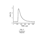
- FIG. 7 shows a typical output pulse from a detector.
- the signal height is related to the ratio of the energy of the detected x-ray and the heat capacity of the detector.
- the pulse height can be increased by reducing the thermal conductivity between the absorber and the cold sink, but then the tail will extend further, reducing the number of counts possible per second. Reducing the size of the detector reduces its heat capacity, thereby increasing the signal height. Using multiple detectors allows each detector to be smaller, thereby increasing the signal height and improving resolution.
- the size of the x-ray image in the focal plane of the x-ray optic will depend on the design and focal length of the optic. If the image is significantly smaller than the area occupied by the multiple sensors, then the sensors can be moved away from the focal plane until the x-ray image occupies most of the sensor array area. Because the x-ray image is typically circular and the detector array is not, as the image is further defocused and becomes larger, some of the x-rays will impact outside of the detector array. Skilled persons will be able to determine an optimum position for the detector array so that the x-rays are sufficiently spread among the detectors to provide a high pulse count rate, while minimizing x-rays that fall outside the detector area.
- the output of the multiple detectors are preferably multiplexed into a single JFET pre-amplifier, as described in U.S. Pat. No. 6,310,350 .
- a preferred dual beam can optionally employ:
- the electron beam scan rate is defined relative to the inverse of the x-ray map acquisition time.
- a fast scan rate is preferably 10 times greater than the inverse of the map acquisition time, more preferably 100 times greater, and more preferably still 1000 times greater.
- the x-ray map acquisition time is 10 minutes, then the frame time is preferably 60 s, more preferably, 6 sec, and most preferably shorter than 0.6 sec.
- High speed electron beam scanning and periodic RF plasma cleaning of the sample e.g., a 20 sec plasma clean once every 5 min
- Gases that can be used for plasma cleaning include air, H 2 O, O 2 and H 2 .
- gases are preferably injected in small quantities using a capillary-style gas injection system.
- a heating stage to gently heat the sample (e.g., up to 50, 100 or 150° C) in order to minimize contamination buildup during x-ray mapping.
- the ion beam can also be used to expose buried sample features for X-ray analysis.
- Embodiments of the invention can also be used for high resolution imaging of stained biological tissue, and tissue labeled with functionalized x-ray tags. Such imaging modes can optionally be applied to thin bio samples, and combined with in-situ scanning transmission electron microscopy (STEM) imaging in order to achieve correlative microscopy.
- STEM scanning transmission electron microscopy
- Optimal correlative microscopy will likely be achieved by performing x-ray mapping using a low beam energy (e.g., 1.5 to 5 keV, in order to maximize the x-ray fluorescence efficiency of nano-scale tags and thin bio tissue) and STEM using an elevated beam energy (e.g., 10 to 30 keV).
- a low beam energy e.g. 1.5 to 5 keV, in order to maximize the x-ray fluorescence efficiency of nano-scale tags and thin bio tissue
- STEM an elevated beam energy
- Embodiments of the invention include the use materials that are optimal for x-ray tags - i.e., materials, such as Mg, Al and Si that exhibit a good compromise between stopping power and efficient, characteristic, low energy x-ray emission lines.
- analyses using low energy K lines are preferred over L lines and L lines are preferred over M lines; however, the stopping power of materials with low energy K lines is typically lower than that of materials with low energy L & M lines, so a skilled person can determine single and multi-element materials that are expected to be optimal as a function of beam energy and tag diameter, for example, by using Monte Carlo simulations.
- Embodiments of the invention enable three-dimensional, high resolution x-ray mapping.
- Three-dimensional, high resolution x-ray mapping has different system requirements compared to conventional EDS mapping because conventional EDS mapping is typically performed at low magnifications, using high electron beam energies.
- Prior art microcalorimetry-based x-ray mapping is limited by shot noise due to very low count rates.
- Applicants have developed a system to characterize a microcalorimeter-type EDS system using a "figure of merit" (FOM) that can be determined for various systems.
- the figure of merit represents the x-ray count in each peak per unit charge injected into the sample by the electron beam.
- the figure of merit therefore has units of x-ray counts per nano Coulomb (nC -1 ).
- the figure of merit of a particular system will depend on the x-ray fluorescence efficiency, x-ray absorption rate inside the sample, and on the efficiency of the collection and detection system. That is, a detector that detects x-rays over a larger solid angle will have a higher figure of merit.
- a figure of merit of at least 100 nC -1 is preferred for characteristic x-rays emitted from a major constituent of the sample volume interrogated by the electron beam, in order for the EDS system to provide a sufficient signal to form an x-ray map with an acceptable signal-to-noise ratio in a reasonable period of time, for example, less than about 20 minutes.
- a system having a figure of merit of less than 100 nC -1 would require too large of a beam current to yield a sufficient x-ray signal-to-noise ratio in a reasonable time.
- the count rate corresponding to a particular FOM i.e., a particular signal-to-noise ratio
- the collection efficiency is fixed and the count rate can be increased by increasing the beam current.
- the figure of merit is a single quantity that can be used to quantify the effectiveness of a microcalorimeter x-ray detector at x-ray mapping, and to quantify the corresponding x-ray count rate at a given beam current.
- the minimum preferred figure of merit of 100 nC -1 derives from the assumption that an x-ray map should include at least 100 pixels by 100 pixels, the beam current should be smaller than or equal to 1 nA and map acquisition should not take longer than 16.7 minutes to perform.
- applicants have been able to create embodiments of the invention that provide unexpected improvements over the prior art and are practical for two-dimensional or three-dimensional x-ray mapping with high spatial resolution, and with maps having 100 pixels by 100 pixels, or more.
- N is the minimum number of pixels needed to form an x-ray map (e.g., 100 x 100)
- X is the minimum number of x-ray counts per pixel in a single x-ray peak (e.g., 10, corresponding to a shot noise-limited signal-to-noise ratio of 10 0.5 ⁇ 3.2)
- I is the maximum acceptable beam current (e.g., 1 nA)
- T is the maximum acceptable map acquisition time (e.g., 10 to 20 minutes)
- an x-ray map of 100 pixels by 100 pixels providing 10 counts per pixel in an x-ray peak that is obtained using a beam current of 1 nA over a time period of 16.7 minutes provides a figure of merit of 100 nC -1 and a shot noise-limited signal-to-noise ratio of approximately 3.2.
- the FOM can be scaled arbitrarily by relaxing or tightening the above data collection parameters.
- the above values are defined to represent the limits that are preferably met or exceeded to enable practical high spatial resolution x-ray mapping.
- the FOM is a function of the maximum acceptable map acquisition time (T) and, at a given electron beam current, the FOM translates to a specific x-ray count rate, and hence defines the number of detectors needed to avoid pulse pileup artifacts.
- T maximum acceptable map acquisition time
- the above values of N, X, I and T yield a count rate of 100 cps per x-ray peak.
- an x-ray spectrum may contain, for example, 5 peaks, and a high quality microcalorimeter may have an FOM of 1000 nC -1 at each peak, translating to an x-ray arrival rate of 5000 cps at the detector array when using an electron beam current of 1 nA.
- the maximum count rate of a single detector is, for example, 500 cps
- an array of more than 10 detectors is needed to avoid pulse pileup artifacts (i.e., 500 cps per detector plus additional detectors needed to process x-rays comprising the Bremsstrahlung background radiation).
- Table I shows the effect of electron beam current and count rate on map acquisition times corresponding to a figure of merit of 100 nC -1 .
- Table 1 Current (nA) Counts/sec (CPS) Time per Pixel (sec) Time per line (min) Time per map (min) 1 0.01 1 10 16.67 1666.67 2 0.1 10 1 1.67 166.67 3 1 100 0.1 .17 16.67 4 10 1000 0.01 .02 1.37 5 100 10000 0.001 0.00 .017
- mapping times for some configurations in Table 1 are impractically long, and the count rates for others would require a large number of detectors to avoid pulse pileup artifacts.
- the electron beam current increases from 0.01 nA to 100 nA, more x-ray photons are generated per unit time by the electron beam and delivered to the sample.
- the detector were capable of the count rates in the second column, the third through fifth column describes the times required per pixel, per 100 pixel line, and per 100 x 100 pixel map. Applicants have determined that less than 20 minutes is an acceptable time in many cases to determine a 100 x 100 pixel map, and a count rate of 100 counts per second is achievable at 1 nA, as described in the third row of the Table 1.
- FIG. 8 illustrates the figure of merit for a number of characteristic x-ray peaks excited in single element materials by a 5 keV electron beam, corresponding to:
- FIG. 9 shows an overall graph 902 of an x-ray spectrum, and smaller graphs 904, 906, and 908 showing enlarged portions of graph 902.
- the Mg K ⁇ peak designated by reference number 910 has a figure of merit of 12.9 nC -1 .
- the figure of merit improves to 387 nC -1 and when the glass capillary with a 20° opening angle is used, the figure of merit increases to 7367 nC -1 , which corresponds to a count rate of 764 cps when using an electron beam current of 100 pA.
- Such a count rate can be processed by two or three detectors.
- the count rate would increase to 7640 cps, and additional detectors would be required to avoid pulse pileup. Similarly, if there are 10 x-ray lines of equal intensity, then a count rate of 7640 cps would need to be accommodated at a beam current of 100 pA.
- the Oxygen K ⁇ peak from the native oxide overlayer has a figure of merit of 3.7 nC -1 for a typical prior art system, 111 nC -1 for a system using an improved glass capillary with a wider acceptance angle, and 2190 nC -1 for a system using an improved glass capillary with a 20° acceptance angle.
- Preferred embodiments of the invention provide a figure of merit for the Au M line emitted from bulk Au irradiated by 5 keV electrons of greater than 100 nC -1 , and more preferably provide a figure of merit greater than 1000 nC -1 .
- Some embodiments provide a figure of merit for the Mg K line of bulk Mg (containing a native oxide) irradiated by 5 keV electrons greater than 500 nC -1 , and more preferably provide a figure of merit greater than 1000 nC -1 .
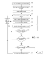
- FIG. 10 shows a preferred method in accordance with the present invention.
- a sample is positioned in the vacuum chamber of a dual beam system with a microcalorimeter-type EDS of the present invention.
- the sample may be, for example, a semiconductor circuit or a biological sample.
- the sample chamber is evacuated to a suitable pressure, depending on the sample.
- an ion beam or a plasma is directed toward the surface of the sample to clean the surface.
- an electron beam is directed toward a point on the substrate surface.
- the beam preferably has an energy of between 2000 eV and 7000 eV, typically about 4,000 eV or less and a beam current of between 0.01 nA and 2 nA, typically 0.5 nA.
- the beam preferably has a spot size of less than 30 nm and more preferably less than 15 nm, and even more preferably 10 nm or less. As the electrons impact the surface, x-rays are emitted from the point in step 1010.
- the x-rays are conducted by an x-ray optic from the sample surface and from the optic to x-ray detectors.
- the detectors determine the energies of the x-rays received while the electron beam is at the first point.
- Decision block 1016 determines when a predetermined dwell period has passed or when a sufficient number of x-rays have been detected to determine the material present at the first point at a sufficient signal-to-noise ratio.
- the electron beam remains directed to the same point for a predetermined dwell time, which is sufficient to determine the composition of the point to a desired accuracy.
- the dwell time required at each point will depend on the electron beam current and the type of material.
- the electron beam is positioned at each point for a sufficient time so that at least ten counts are registered for each x-ray peak present.
- the electron beam remains directed to each point for about 0.1 seconds.
- dwell time varies at different points on the sample surface until a pre-determined number of x-rays is detected, and the dwell time at each point is recorded and used to normalize the number of x-rays detected from each point.
- the electron beam scans an area of at least 100 dwell points by 100 dwell points to form a map with 10,000 pixels.
- the position of the electron beam is optionally recalibrated periodically, for example, by viewing a fiducial, to compensate for drift in the electron beam position.
- the ion beam removes a layer of material in step 1032.
- the ion beam may remove about 20 nm.
- the ion beam may be used with a precursor gas to assist etching or may simply sputter material. Skilled persons can readily determine the required ion beam parameters for removing a layer.
- the process of mapping the new layer begins again with step 1008.
- the electron beam is scanned rapidly and repeatedly over the sample region of interest.
- the data collection system records the energy of each x-ray detected by the microcalorimeter, as well as the electron beam position at the sample surface.
- the data collection system records the energy of each x-ray and the time at which each x-ray is detected.
- the time information is then used to calculate the electron beam position corresponding to each x-ray detection event and to construct an x-ray map.
- the x-ray map can either be constructed in real time, during analysis, or after data collection is complete.
- the fast scanning method has the advantage that a large number of electron images can be collected during x-ray detection.
- the emission rate of electrons is typically much greater than the emission rate of x-rays from the sample.
- Common secondary and backscattered electron detectors such as the Everhart-Thornley scintillator-photomultiplier detector and the Si solid state detector can be used for electron imaging. If the sample is sufficiently thin, transmitted electrons can also be used to form electron images. The electron images can be used to recalibrate the electron beam position periodically to correct for sample or beam drift occurring during x-ray mapping.
- the multi-detector array can be placed into or outside the focal plane of the optic so as to maximize the x-ray collection efficiency and minimize the maximum x-ray flux incident onto any single detector.
- the dual beam system provides an electron beam (for low energy, high resolution x-ray mapping) and a means to remove surface material from the sample (to enable depth-resolved x-ray analysis). Material removal is preferably performed by a focused ion beam, but can also be achieved using a broad ion source, a plasma source, or a laser.
- the invention has broad applicability and can provide many benefits as described and shown in the examples above.
- the embodiments will vary greatly depending upon the specific application, and not every embodiment will provide all of the benefits and meet all of the objectives that are achievable by the invention.
Landscapes
- Chemical & Material Sciences (AREA)
- Analytical Chemistry (AREA)
- Crystallography & Structural Chemistry (AREA)
- Physics & Mathematics (AREA)
- Health & Medical Sciences (AREA)
- Life Sciences & Earth Sciences (AREA)
- Biochemistry (AREA)
- General Health & Medical Sciences (AREA)
- General Physics & Mathematics (AREA)
- Immunology (AREA)
- Pathology (AREA)
- Analysing Materials By The Use Of Radiation (AREA)
Applications Claiming Priority (1)
| Application Number | Priority Date | Filing Date | Title |
|---|---|---|---|
| US23277909P | 2009-08-10 | 2009-08-10 |
Publications (3)
| Publication Number | Publication Date |
|---|---|
| EP2284524A2 true EP2284524A2 (de) | 2011-02-16 |
| EP2284524A3 EP2284524A3 (de) | 2011-06-01 |
| EP2284524B1 EP2284524B1 (de) | 2014-01-15 |
Family
ID=43334756
Family Applications (1)
| Application Number | Title | Priority Date | Filing Date |
|---|---|---|---|
| EP10171817.9A Active EP2284524B1 (de) | 2009-08-10 | 2010-08-04 | Mikrokalometrie für die Röntgenstrahlspektroskopie |
Country Status (3)
| Country | Link |
|---|---|
| US (1) | US8357894B2 (de) |
| EP (1) | EP2284524B1 (de) |
| JP (1) | JP5698885B2 (de) |
Cited By (3)
| Publication number | Priority date | Publication date | Assignee | Title |
|---|---|---|---|---|
| CZ303228B6 (cs) * | 2011-03-23 | 2012-06-06 | Tescan A.S. | Zpusob analýzy materiálu fokusovaným elektronovým svazkem s využitím charakteristického rentgenového zárení a zpetne odražených elektronu a zarízení k jeho provádení |
| WO2017210203A1 (en) * | 2016-05-31 | 2017-12-07 | EDAX, Incorporated | Systems and methods for adaptive scanning |
| CN109313146A (zh) * | 2016-03-14 | 2019-02-05 | X射线光学系统公司 | 用于加压流体的样品处理设备和其x射线分析器应用 |
Families Citing this family (36)
| Publication number | Priority date | Publication date | Assignee | Title |
|---|---|---|---|---|
| WO2011146758A2 (en) * | 2010-05-19 | 2011-11-24 | Silver Eric H | Hybrid x-ray optic apparatus and methods |
| US20150117599A1 (en) | 2013-10-31 | 2015-04-30 | Sigray, Inc. | X-ray interferometric imaging system |
| US9091628B2 (en) | 2012-12-21 | 2015-07-28 | L-3 Communications Security And Detection Systems, Inc. | 3D mapping with two orthogonal imaging views |
| GB201308436D0 (en) * | 2013-05-10 | 2013-06-19 | Oxford Instr Nanotechnology Tools Ltd | Metrology for preparation of thin samples |
| EP2848924B1 (de) * | 2013-09-11 | 2016-08-24 | Anton Paar GmbH | Temperierkammer für kompaktes Röntgengerät |
| US10269528B2 (en) | 2013-09-19 | 2019-04-23 | Sigray, Inc. | Diverging X-ray sources using linear accumulation |
| US10295485B2 (en) | 2013-12-05 | 2019-05-21 | Sigray, Inc. | X-ray transmission spectrometer system |
| US10297359B2 (en) | 2013-09-19 | 2019-05-21 | Sigray, Inc. | X-ray illumination system with multiple target microstructures |
| US10304580B2 (en) | 2013-10-31 | 2019-05-28 | Sigray, Inc. | Talbot X-ray microscope |
| USRE48612E1 (en) | 2013-10-31 | 2021-06-29 | Sigray, Inc. | X-ray interferometric imaging system |
| US9523777B2 (en) * | 2014-04-10 | 2016-12-20 | Uchicago Argonne, Llc | Thermal kinetic inductance detector |
| US20150293042A1 (en) * | 2014-04-11 | 2015-10-15 | Semiconductor Energy Laboratory Co., Ltd. | Measurement Device and Measurement Method |
| US10401309B2 (en) | 2014-05-15 | 2019-09-03 | Sigray, Inc. | X-ray techniques using structured illumination |
| US9696268B2 (en) | 2014-10-27 | 2017-07-04 | Kla-Tencor Corporation | Automated decision-based energy-dispersive x-ray methodology and apparatus |
| US10352880B2 (en) | 2015-04-29 | 2019-07-16 | Sigray, Inc. | Method and apparatus for x-ray microscopy |
| US10295486B2 (en) | 2015-08-18 | 2019-05-21 | Sigray, Inc. | Detector for X-rays with high spatial and high spectral resolution |
| JP6589461B2 (ja) * | 2015-08-26 | 2019-10-16 | 株式会社日立ハイテクサイエンス | X線分析装置 |
| JP6745621B2 (ja) * | 2016-03-24 | 2020-08-26 | 株式会社日立ハイテクサイエンス | 放射線分析装置、及び放射線分析方法 |
| US10274440B2 (en) * | 2016-06-22 | 2019-04-30 | International Business Machines Corporation | Method to facilitate investigation of chemical constituents in chemical analysis data |
| US10247683B2 (en) | 2016-12-03 | 2019-04-02 | Sigray, Inc. | Material measurement techniques using multiple X-ray micro-beams |
| JP6937380B2 (ja) * | 2017-03-22 | 2021-09-22 | シグレイ、インコーポレイテッド | X線分光を実施するための方法およびx線吸収分光システム |
| JP6998034B2 (ja) * | 2017-07-25 | 2022-01-18 | 株式会社日立ハイテクサイエンス | 放射線分析装置 |
| US10914694B2 (en) * | 2017-08-23 | 2021-02-09 | Government Of The United States Of America, As Represented By The Secretary Of Commerce | X-ray spectrometer |
| US10345249B1 (en) * | 2017-12-15 | 2019-07-09 | The United States Of America, As Represented By The Secretary Of Commerce | System for detecting and real time processing x-ray pulses from microcalorimeter detectors |
| JP6954848B2 (ja) * | 2018-01-24 | 2021-10-27 | 日本電子株式会社 | 走査電子顕微鏡および測定方法 |
| US10578566B2 (en) | 2018-04-03 | 2020-03-03 | Sigray, Inc. | X-ray emission spectrometer system |
| US10845491B2 (en) | 2018-06-04 | 2020-11-24 | Sigray, Inc. | Energy-resolving x-ray detection system |
| DE112019003777B4 (de) | 2018-07-26 | 2025-09-11 | Sigray, Inc. | Röntgenreflexionsquelle mit hoher helligkeit |
| US10656105B2 (en) | 2018-08-06 | 2020-05-19 | Sigray, Inc. | Talbot-lau x-ray source and interferometric system |
| DE112019004433B4 (de) | 2018-09-04 | 2024-09-12 | Sigray, Inc. | System und verfahren für röntgenstrahlfluoreszenz mit filterung |
| WO2020051221A2 (en) | 2018-09-07 | 2020-03-12 | Sigray, Inc. | System and method for depth-selectable x-ray analysis |
| CN109696447B (zh) * | 2018-12-29 | 2020-10-16 | 苏州瑞派宁科技有限公司 | 一种软x射线显微成像装置 |
| WO2021162947A1 (en) | 2020-02-10 | 2021-08-19 | Sigray, Inc. | X-ray mirror optics with multiple hyperboloidal / hyperbolic surface profiles |
| CN113008920B (zh) * | 2021-03-04 | 2023-03-21 | 上海科技大学 | 用于x射线自由电子激光装置的小型样品腔 |
| DE102021117592B9 (de) | 2021-07-07 | 2023-08-03 | Carl Zeiss Microscopy Gmbh | Verfahren zum Betreiben eines Teilchenstrahlmikroskops, Teilchenstrahlmikroskop und Computerprogrammprodukt |
| GB202208289D0 (en) * | 2022-06-06 | 2022-07-20 | Oxford Instruments Nanotechnology Tools Ltd | Ebsd data enhancement using simulated pattern matching |
Citations (4)
| Publication number | Priority date | Publication date | Assignee | Title |
|---|---|---|---|---|
| US5880467A (en) | 1997-03-05 | 1999-03-09 | The United States Of America As Represented By The Secretary Of Commerce | Microcalorimeter x-ray detectors with x-ray lens |
| US6094471A (en) | 1998-04-22 | 2000-07-25 | Smithsonian Astrophysical Observatory | X-ray diagnostic system |
| US6310350B1 (en) | 1998-09-24 | 2001-10-30 | Eric H. Silver | Multiplexed microcalorimeter array |
| US6479818B1 (en) | 1998-09-17 | 2002-11-12 | Thermo Noran Inc. | Application of x-ray optics to energy dispersive spectroscopy |
Family Cites Families (18)
| Publication number | Priority date | Publication date | Assignee | Title |
|---|---|---|---|---|
| JP3252410B2 (ja) * | 1991-10-22 | 2002-02-04 | ソニー株式会社 | 微小領域物性測定装置 |
| US5389792A (en) * | 1993-01-04 | 1995-02-14 | Grumman Aerospace Corporation | Electron microprobe utilizing thermal detector arrays |
| JPH08226904A (ja) * | 1995-02-21 | 1996-09-03 | Hitachi Ltd | 分析電子顕微鏡及び分析方法 |
| US5777336A (en) * | 1995-10-03 | 1998-07-07 | The Regents Of The University Of California | Broadband high resolution X-ray spectral analyzer |
| JPH1012684A (ja) * | 1996-06-26 | 1998-01-16 | Hitachi Ltd | 半導体装置の検査方法及びその装置 |
| JP4007305B2 (ja) * | 1997-05-08 | 2007-11-14 | 株式会社日立製作所 | 電子顕微鏡の分解能評価方法および電子顕微鏡の調整方法 |
| JP3123602B2 (ja) * | 1998-03-02 | 2001-01-15 | 日本電気株式会社 | 深さ方向組成分布分析方法 |
| WO2000004357A1 (en) * | 1998-07-15 | 2000-01-27 | Smithsonian Astrophysical Observatory | Epitaxial germanium temperature sensor |
| JP2003075544A (ja) * | 2001-09-05 | 2003-03-12 | National Institute Of Advanced Industrial & Technology | 超伝導放射線検出器 |
| JP4314921B2 (ja) * | 2003-03-18 | 2009-08-19 | 株式会社島津製作所 | 放射線検出器 |
| EP1501115B1 (de) * | 2003-07-14 | 2009-07-01 | FEI Company | Zweistrahlsystem |
| JP2005249558A (ja) * | 2004-03-04 | 2005-09-15 | Shimadzu Corp | X線分析装置 |
| JP2006173038A (ja) * | 2004-12-20 | 2006-06-29 | Hitachi High-Technologies Corp | 荷電粒子線装置、試料像表示方法及びイメージシフト感度計測方法 |
| JP2006226800A (ja) * | 2005-02-17 | 2006-08-31 | Sii Nanotechnology Inc | 超伝導x線検出装置及びそれを用いた超伝導x線分析装置 |
| JP2006242664A (ja) * | 2005-03-02 | 2006-09-14 | Sii Nanotechnology Inc | 3次元構造物分析システム |
| JP2007225363A (ja) * | 2006-02-22 | 2007-09-06 | Hitachi Ltd | 磁気試料検査装置 |
| JP4307470B2 (ja) * | 2006-08-08 | 2009-08-05 | 株式会社日立ハイテクノロジーズ | 荷電粒子線装置、試料加工方法及び半導体検査装置 |
| US8080791B2 (en) * | 2008-12-12 | 2011-12-20 | Fei Company | X-ray detector for electron microscope |
-
2010
- 2010-08-04 EP EP10171817.9A patent/EP2284524B1/de active Active
- 2010-08-09 JP JP2010178673A patent/JP5698885B2/ja not_active Expired - Fee Related
- 2010-08-10 US US12/853,998 patent/US8357894B2/en not_active Expired - Fee Related
Patent Citations (4)
| Publication number | Priority date | Publication date | Assignee | Title |
|---|---|---|---|---|
| US5880467A (en) | 1997-03-05 | 1999-03-09 | The United States Of America As Represented By The Secretary Of Commerce | Microcalorimeter x-ray detectors with x-ray lens |
| US6094471A (en) | 1998-04-22 | 2000-07-25 | Smithsonian Astrophysical Observatory | X-ray diagnostic system |
| US6479818B1 (en) | 1998-09-17 | 2002-11-12 | Thermo Noran Inc. | Application of x-ray optics to energy dispersive spectroscopy |
| US6310350B1 (en) | 1998-09-24 | 2001-10-30 | Eric H. Silver | Multiplexed microcalorimeter array |
Non-Patent Citations (1)
| Title |
|---|
| "High Resoultion X-Ray Spectroscopy with a Microcalorimeter", U.S. DEPARTMENT OF ENERQV JOURNAL OF UNDERQRADUATE RESEARCH, vol. 5, 2005, Retrieved from the Internet <URL:http://vvww.scied .science.doe.qov/scied/J U R v5/default.htm> |
Cited By (4)
| Publication number | Priority date | Publication date | Assignee | Title |
|---|---|---|---|---|
| CZ303228B6 (cs) * | 2011-03-23 | 2012-06-06 | Tescan A.S. | Zpusob analýzy materiálu fokusovaným elektronovým svazkem s využitím charakteristického rentgenového zárení a zpetne odražených elektronu a zarízení k jeho provádení |
| CN109313146A (zh) * | 2016-03-14 | 2019-02-05 | X射线光学系统公司 | 用于加压流体的样品处理设备和其x射线分析器应用 |
| US10705033B2 (en) | 2016-03-14 | 2020-07-07 | X-Ray Optical Systems, Inc. | Sample handling apparatus for pressurized fluids and X-ray analyzer applications thereof |
| WO2017210203A1 (en) * | 2016-05-31 | 2017-12-07 | EDAX, Incorporated | Systems and methods for adaptive scanning |
Also Published As
| Publication number | Publication date |
|---|---|
| EP2284524A3 (de) | 2011-06-01 |
| JP5698885B2 (ja) | 2015-04-08 |
| US20110064191A1 (en) | 2011-03-17 |
| JP2011039053A (ja) | 2011-02-24 |
| US8357894B2 (en) | 2013-01-22 |
| EP2284524B1 (de) | 2014-01-15 |
Similar Documents
| Publication | Publication Date | Title |
|---|---|---|
| EP2284524B1 (de) | Mikrokalometrie für die Röntgenstrahlspektroskopie | |
| Wollman et al. | High‐resolution, energy‐dispersive microcalorimeter spectrometer for X‐ray microanalysis | |
| Ryll et al. | A pnCCD-based, fast direct single electron imaging camera for TEM and STEM | |
| Sekiguchi et al. | Quantitative electron‐beam tester for defects in semiconductors (CL/EBIC/SDLTS system) | |
| JP4885740B2 (ja) | 超伝導x線検出器およびそれを用いたx線分析装置 | |
| Ngo | Energy dispersive spectroscopy | |
| US9778377B2 (en) | Method of performing spectroscopy in a transmission charged-particle microscope | |
| US7952073B2 (en) | Apparatus and method including a direct bombardment detector and a secondary detector for use in electron microscopy | |
| Patt et al. | Bulk sensitive hard x-ray photoemission electron microscopy | |
| US20190341243A1 (en) | Eels detection technique in an electron microscope | |
| JP2018190705A (ja) | 荷電粒子源の放出雑音補正 | |
| CN116802765A (zh) | 时间解析阴极发光样本探测 | |
| US5880467A (en) | Microcalorimeter x-ray detectors with x-ray lens | |
| Longoni et al. | A novel high‐resolution XRF spectrometer for elemental mapping based on a monolithic array of silicon drift detectors and on a polycapillary x‐ray lens | |
| Newbury | Electron-excited energy dispersive X-ray spectrometry at high speed and at high resolution: silicon drift detectors and microcalorimeters | |
| Alberti et al. | Use of silicon drift detectors for the detection of medium-light elements in PIXE | |
| Emberger et al. | Total ionizing dose test with DEPFET sensors for Athena's WFI | |
| Longoni et al. | XRF spectrometers based on monolithic arrays of silicon drift detectors: Elemental mapping analyses and advanced detector structures | |
| Alberti et al. | Performance evaluation of an advanced xrf elemental mapping system featuring a novel ring-shaped monolithic array of silicon drift detectors | |
| US20060198494A1 (en) | Three-dimensional structure analyzing system | |
| Simionovici et al. | New results in X-ray computed fluorescence tomography | |
| Takano et al. | X-ray transmission characteristic measurements of polycapillary optics installed in an analytical electron microscope | |
| Nakamura et al. | Nanoscale X-ray Tomography of Integrated Circuits using a Hybrid Electron/X-ray Microscope: Results and Prospects | |
| Takano et al. | X-ray transmission characteristics measurement of a polycapillary lens installed in an analytical electron microscope | |
| Takano et al. | Characterization of Polycapillary Optics Installed in an Analytical Electron Microscope |
Legal Events
| Date | Code | Title | Description |
|---|---|---|---|
| PUAI | Public reference made under article 153(3) epc to a published international application that has entered the european phase |
Free format text: ORIGINAL CODE: 0009012 |
|
| AK | Designated contracting states |
Kind code of ref document: A2 Designated state(s): AL AT BE BG CH CY CZ DE DK EE ES FI FR GB GR HR HU IE IS IT LI LT LU LV MC MK MT NL NO PL PT RO SE SI SK SM TR |
|
| AX | Request for extension of the european patent |
Extension state: BA ME RS |
|
| PUAL | Search report despatched |
Free format text: ORIGINAL CODE: 0009013 |
|
| AK | Designated contracting states |
Kind code of ref document: A3 Designated state(s): AL AT BE BG CH CY CZ DE DK EE ES FI FR GB GR HR HU IE IS IT LI LT LU LV MC MK MT NL NO PL PT RO SE SI SK SM TR |
|
| AX | Request for extension of the european patent |
Extension state: BA ME RS |
|
| RIC1 | Information provided on ipc code assigned before grant |
Ipc: H01J 37/244 20060101ALI20110428BHEP Ipc: H01J 37/256 20060101ALI20110428BHEP Ipc: G01N 23/20 20060101AFI20101222BHEP Ipc: G01N 23/225 20060101ALI20110428BHEP |
|
| 17P | Request for examination filed |
Effective date: 20111201 |
|
| 17Q | First examination report despatched |
Effective date: 20120606 |
|
| GRAP | Despatch of communication of intention to grant a patent |
Free format text: ORIGINAL CODE: EPIDOSNIGR1 |
|
| INTG | Intention to grant announced |
Effective date: 20131018 |
|
| GRAS | Grant fee paid |
Free format text: ORIGINAL CODE: EPIDOSNIGR3 |
|
| GRAA | (expected) grant |
Free format text: ORIGINAL CODE: 0009210 |
|
| AK | Designated contracting states |
Kind code of ref document: B1 Designated state(s): AL AT BE BG CH CY CZ DE DK EE ES FI FR GB GR HR HU IE IS IT LI LT LU LV MC MK MT NL NO PL PT RO SE SI SK SM TR |
|
| REG | Reference to a national code |
Ref country code: CH Ref legal event code: EP Ref country code: GB Ref legal event code: FG4D |
|
| REG | Reference to a national code |
Ref country code: AT Ref legal event code: REF Ref document number: 650046 Country of ref document: AT Kind code of ref document: T Effective date: 20140215 |
|
| REG | Reference to a national code |
Ref country code: IE Ref legal event code: FG4D |
|
| REG | Reference to a national code |
Ref country code: DE Ref legal event code: R096 Ref document number: 602010013101 Country of ref document: DE Effective date: 20140227 |
|
| REG | Reference to a national code |
Ref country code: NL Ref legal event code: VDEP Effective date: 20140115 |
|
| REG | Reference to a national code |
Ref country code: AT Ref legal event code: MK05 Ref document number: 650046 Country of ref document: AT Kind code of ref document: T Effective date: 20140115 |
|
| REG | Reference to a national code |
Ref country code: LT Ref legal event code: MG4D |
|
| PG25 | Lapsed in a contracting state [announced via postgrant information from national office to epo] |
Ref country code: LT Free format text: LAPSE BECAUSE OF FAILURE TO SUBMIT A TRANSLATION OF THE DESCRIPTION OR TO PAY THE FEE WITHIN THE PRESCRIBED TIME-LIMIT Effective date: 20140115 Ref country code: NO Free format text: LAPSE BECAUSE OF FAILURE TO SUBMIT A TRANSLATION OF THE DESCRIPTION OR TO PAY THE FEE WITHIN THE PRESCRIBED TIME-LIMIT Effective date: 20140415 Ref country code: IS Free format text: LAPSE BECAUSE OF FAILURE TO SUBMIT A TRANSLATION OF THE DESCRIPTION OR TO PAY THE FEE WITHIN THE PRESCRIBED TIME-LIMIT Effective date: 20140515 |
|
| PG25 | Lapsed in a contracting state [announced via postgrant information from national office to epo] |
Ref country code: NL Free format text: LAPSE BECAUSE OF FAILURE TO SUBMIT A TRANSLATION OF THE DESCRIPTION OR TO PAY THE FEE WITHIN THE PRESCRIBED TIME-LIMIT Effective date: 20140115 Ref country code: SE Free format text: LAPSE BECAUSE OF FAILURE TO SUBMIT A TRANSLATION OF THE DESCRIPTION OR TO PAY THE FEE WITHIN THE PRESCRIBED TIME-LIMIT Effective date: 20140115 Ref country code: PT Free format text: LAPSE BECAUSE OF FAILURE TO SUBMIT A TRANSLATION OF THE DESCRIPTION OR TO PAY THE FEE WITHIN THE PRESCRIBED TIME-LIMIT Effective date: 20140515 Ref country code: AT Free format text: LAPSE BECAUSE OF FAILURE TO SUBMIT A TRANSLATION OF THE DESCRIPTION OR TO PAY THE FEE WITHIN THE PRESCRIBED TIME-LIMIT Effective date: 20140115 Ref country code: FI Free format text: LAPSE BECAUSE OF FAILURE TO SUBMIT A TRANSLATION OF THE DESCRIPTION OR TO PAY THE FEE WITHIN THE PRESCRIBED TIME-LIMIT Effective date: 20140115 Ref country code: ES Free format text: LAPSE BECAUSE OF FAILURE TO SUBMIT A TRANSLATION OF THE DESCRIPTION OR TO PAY THE FEE WITHIN THE PRESCRIBED TIME-LIMIT Effective date: 20140115 Ref country code: CY Free format text: LAPSE BECAUSE OF FAILURE TO SUBMIT A TRANSLATION OF THE DESCRIPTION OR TO PAY THE FEE WITHIN THE PRESCRIBED TIME-LIMIT Effective date: 20140115 |
|
| PG25 | Lapsed in a contracting state [announced via postgrant information from national office to epo] |
Ref country code: BE Free format text: LAPSE BECAUSE OF FAILURE TO SUBMIT A TRANSLATION OF THE DESCRIPTION OR TO PAY THE FEE WITHIN THE PRESCRIBED TIME-LIMIT Effective date: 20140115 Ref country code: HR Free format text: LAPSE BECAUSE OF FAILURE TO SUBMIT A TRANSLATION OF THE DESCRIPTION OR TO PAY THE FEE WITHIN THE PRESCRIBED TIME-LIMIT Effective date: 20140115 Ref country code: LV Free format text: LAPSE BECAUSE OF FAILURE TO SUBMIT A TRANSLATION OF THE DESCRIPTION OR TO PAY THE FEE WITHIN THE PRESCRIBED TIME-LIMIT Effective date: 20140115 |
|
| REG | Reference to a national code |
Ref country code: DE Ref legal event code: R097 Ref document number: 602010013101 Country of ref document: DE |
|
| PG25 | Lapsed in a contracting state [announced via postgrant information from national office to epo] |
Ref country code: EE Free format text: LAPSE BECAUSE OF FAILURE TO SUBMIT A TRANSLATION OF THE DESCRIPTION OR TO PAY THE FEE WITHIN THE PRESCRIBED TIME-LIMIT Effective date: 20140115 Ref country code: DK Free format text: LAPSE BECAUSE OF FAILURE TO SUBMIT A TRANSLATION OF THE DESCRIPTION OR TO PAY THE FEE WITHIN THE PRESCRIBED TIME-LIMIT Effective date: 20140115 Ref country code: RO Free format text: LAPSE BECAUSE OF FAILURE TO SUBMIT A TRANSLATION OF THE DESCRIPTION OR TO PAY THE FEE WITHIN THE PRESCRIBED TIME-LIMIT Effective date: 20140115 Ref country code: CZ Free format text: LAPSE BECAUSE OF FAILURE TO SUBMIT A TRANSLATION OF THE DESCRIPTION OR TO PAY THE FEE WITHIN THE PRESCRIBED TIME-LIMIT Effective date: 20140115 |
|
| PLBE | No opposition filed within time limit |
Free format text: ORIGINAL CODE: 0009261 |
|
| STAA | Information on the status of an ep patent application or granted ep patent |
Free format text: STATUS: NO OPPOSITION FILED WITHIN TIME LIMIT |
|
| PG25 | Lapsed in a contracting state [announced via postgrant information from national office to epo] |
Ref country code: SK Free format text: LAPSE BECAUSE OF FAILURE TO SUBMIT A TRANSLATION OF THE DESCRIPTION OR TO PAY THE FEE WITHIN THE PRESCRIBED TIME-LIMIT Effective date: 20140115 Ref country code: PL Free format text: LAPSE BECAUSE OF FAILURE TO SUBMIT A TRANSLATION OF THE DESCRIPTION OR TO PAY THE FEE WITHIN THE PRESCRIBED TIME-LIMIT Effective date: 20140115 |
|
| 26N | No opposition filed |
Effective date: 20141016 |
|
| REG | Reference to a national code |
Ref country code: DE Ref legal event code: R097 Ref document number: 602010013101 Country of ref document: DE Effective date: 20141016 |
|
| PG25 | Lapsed in a contracting state [announced via postgrant information from national office to epo] |
Ref country code: MC Free format text: LAPSE BECAUSE OF FAILURE TO SUBMIT A TRANSLATION OF THE DESCRIPTION OR TO PAY THE FEE WITHIN THE PRESCRIBED TIME-LIMIT Effective date: 20140115 Ref country code: LU Free format text: LAPSE BECAUSE OF FAILURE TO SUBMIT A TRANSLATION OF THE DESCRIPTION OR TO PAY THE FEE WITHIN THE PRESCRIBED TIME-LIMIT Effective date: 20140804 |
|
| REG | Reference to a national code |
Ref country code: CH Ref legal event code: PL |
|
| PG25 | Lapsed in a contracting state [announced via postgrant information from national office to epo] |
Ref country code: CH Free format text: LAPSE BECAUSE OF NON-PAYMENT OF DUE FEES Effective date: 20140831 Ref country code: LI Free format text: LAPSE BECAUSE OF NON-PAYMENT OF DUE FEES Effective date: 20140831 |
|
| REG | Reference to a national code |
Ref country code: IE Ref legal event code: MM4A |
|
| PG25 | Lapsed in a contracting state [announced via postgrant information from national office to epo] |
Ref country code: SI Free format text: LAPSE BECAUSE OF FAILURE TO SUBMIT A TRANSLATION OF THE DESCRIPTION OR TO PAY THE FEE WITHIN THE PRESCRIBED TIME-LIMIT Effective date: 20140115 |
|
| PG25 | Lapsed in a contracting state [announced via postgrant information from national office to epo] |
Ref country code: IE Free format text: LAPSE BECAUSE OF NON-PAYMENT OF DUE FEES Effective date: 20140804 |
|
| PG25 | Lapsed in a contracting state [announced via postgrant information from national office to epo] |
Ref country code: SM Free format text: LAPSE BECAUSE OF FAILURE TO SUBMIT A TRANSLATION OF THE DESCRIPTION OR TO PAY THE FEE WITHIN THE PRESCRIBED TIME-LIMIT Effective date: 20140115 |
|
| PG25 | Lapsed in a contracting state [announced via postgrant information from national office to epo] |
Ref country code: BG Free format text: LAPSE BECAUSE OF FAILURE TO SUBMIT A TRANSLATION OF THE DESCRIPTION OR TO PAY THE FEE WITHIN THE PRESCRIBED TIME-LIMIT Effective date: 20140115 Ref country code: GR Free format text: LAPSE BECAUSE OF FAILURE TO SUBMIT A TRANSLATION OF THE DESCRIPTION OR TO PAY THE FEE WITHIN THE PRESCRIBED TIME-LIMIT Effective date: 20140416 Ref country code: IT Free format text: LAPSE BECAUSE OF FAILURE TO SUBMIT A TRANSLATION OF THE DESCRIPTION OR TO PAY THE FEE WITHIN THE PRESCRIBED TIME-LIMIT Effective date: 20140115 Ref country code: MT Free format text: LAPSE BECAUSE OF FAILURE TO SUBMIT A TRANSLATION OF THE DESCRIPTION OR TO PAY THE FEE WITHIN THE PRESCRIBED TIME-LIMIT Effective date: 20140115 |
|
| PG25 | Lapsed in a contracting state [announced via postgrant information from national office to epo] |
Ref country code: HU Free format text: LAPSE BECAUSE OF FAILURE TO SUBMIT A TRANSLATION OF THE DESCRIPTION OR TO PAY THE FEE WITHIN THE PRESCRIBED TIME-LIMIT; INVALID AB INITIO Effective date: 20100804 Ref country code: TR Free format text: LAPSE BECAUSE OF FAILURE TO SUBMIT A TRANSLATION OF THE DESCRIPTION OR TO PAY THE FEE WITHIN THE PRESCRIBED TIME-LIMIT Effective date: 20140115 |
|
| REG | Reference to a national code |
Ref country code: FR Ref legal event code: PLFP Year of fee payment: 7 |
|
| REG | Reference to a national code |
Ref country code: FR Ref legal event code: PLFP Year of fee payment: 8 |
|
| PG25 | Lapsed in a contracting state [announced via postgrant information from national office to epo] |
Ref country code: MK Free format text: LAPSE BECAUSE OF FAILURE TO SUBMIT A TRANSLATION OF THE DESCRIPTION OR TO PAY THE FEE WITHIN THE PRESCRIBED TIME-LIMIT Effective date: 20140115 |
|
| REG | Reference to a national code |
Ref country code: FR Ref legal event code: PLFP Year of fee payment: 9 |
|
| PG25 | Lapsed in a contracting state [announced via postgrant information from national office to epo] |
Ref country code: AL Free format text: LAPSE BECAUSE OF FAILURE TO SUBMIT A TRANSLATION OF THE DESCRIPTION OR TO PAY THE FEE WITHIN THE PRESCRIBED TIME-LIMIT Effective date: 20140115 |
|
| PGFP | Annual fee paid to national office [announced via postgrant information from national office to epo] |
Ref country code: DE Payment date: 20240726 Year of fee payment: 15 |
|
| PGFP | Annual fee paid to national office [announced via postgrant information from national office to epo] |
Ref country code: GB Payment date: 20240816 Year of fee payment: 15 |
|
| PGFP | Annual fee paid to national office [announced via postgrant information from national office to epo] |
Ref country code: FR Payment date: 20240814 Year of fee payment: 15 |