EP2267190B1 - Large area, uniformly low dislocation density gan substrate and process for making the same - Google Patents
Large area, uniformly low dislocation density gan substrate and process for making the same Download PDFInfo
- Publication number
- EP2267190B1 EP2267190B1 EP10010831.5A EP10010831A EP2267190B1 EP 2267190 B1 EP2267190 B1 EP 2267190B1 EP 10010831 A EP10010831 A EP 10010831A EP 2267190 B1 EP2267190 B1 EP 2267190B1
- Authority
- EP
- European Patent Office
- Prior art keywords
- growth
- gan
- phase
- pits
- pit
- Prior art date
- Legal status (The legal status is an assumption and is not a legal conclusion. Google has not performed a legal analysis and makes no representation as to the accuracy of the status listed.)
- Active
Links
- 238000000034 method Methods 0.000 title claims abstract description 118
- 230000008569 process Effects 0.000 title claims abstract description 87
- JMASRVWKEDWRBT-UHFFFAOYSA-N Gallium nitride Chemical compound [Ga]#N JMASRVWKEDWRBT-UHFFFAOYSA-N 0.000 title description 220
- 230000012010 growth Effects 0.000 claims abstract description 317
- 239000000463 material Substances 0.000 claims abstract description 126
- 239000000758 substrate Substances 0.000 claims abstract description 61
- 238000011049 filling Methods 0.000 claims abstract description 53
- 150000004767 nitrides Chemical class 0.000 claims abstract description 47
- QGZKDVFQNNGYKY-UHFFFAOYSA-N Ammonia Chemical compound N QGZKDVFQNNGYKY-UHFFFAOYSA-N 0.000 claims abstract description 45
- 239000012071 phase Substances 0.000 claims abstract description 43
- 239000013078 crystal Substances 0.000 claims abstract description 35
- VEXZGXHMUGYJMC-UHFFFAOYSA-N Hydrochloric acid Chemical compound Cl VEXZGXHMUGYJMC-UHFFFAOYSA-N 0.000 claims abstract description 30
- 229910000041 hydrogen chloride Inorganic materials 0.000 claims abstract description 29
- IXCSERBJSXMMFS-UHFFFAOYSA-N hydrogen chloride Substances Cl.Cl IXCSERBJSXMMFS-UHFFFAOYSA-N 0.000 claims abstract description 29
- 230000007547 defect Effects 0.000 claims abstract description 18
- 229910021529 ammonia Inorganic materials 0.000 claims abstract description 13
- 238000001947 vapour-phase growth Methods 0.000 claims abstract description 11
- 238000002248 hydride vapour-phase epitaxy Methods 0.000 claims description 22
- 229910052594 sapphire Inorganic materials 0.000 claims description 12
- 239000010980 sapphire Substances 0.000 claims description 12
- XUIMIQQOPSSXEZ-UHFFFAOYSA-N Silicon Chemical compound [Si] XUIMIQQOPSSXEZ-UHFFFAOYSA-N 0.000 claims description 7
- 229910052710 silicon Inorganic materials 0.000 claims description 7
- 239000010703 silicon Substances 0.000 claims description 7
- 239000010432 diamond Substances 0.000 claims description 5
- 229910003460 diamond Inorganic materials 0.000 claims description 5
- JBRZTFJDHDCESZ-UHFFFAOYSA-N AsGa Chemical compound [As]#[Ga] JBRZTFJDHDCESZ-UHFFFAOYSA-N 0.000 claims description 4
- 229910001218 Gallium arsenide Inorganic materials 0.000 claims description 4
- XLOMVQKBTHCTTD-UHFFFAOYSA-N Zinc monoxide Chemical compound [Zn]=O XLOMVQKBTHCTTD-UHFFFAOYSA-N 0.000 claims description 4
- JFBZPFYRPYOZCQ-UHFFFAOYSA-N [Li].[Al] Chemical compound [Li].[Al] JFBZPFYRPYOZCQ-UHFFFAOYSA-N 0.000 claims description 2
- LNTHITQWFMADLM-UHFFFAOYSA-N gallic acid Chemical compound OC(=O)C1=CC(O)=C(O)C(O)=C1 LNTHITQWFMADLM-UHFFFAOYSA-N 0.000 claims description 2
- YQNQTEBHHUSESQ-UHFFFAOYSA-N lithium aluminate Chemical compound [Li+].[O-][Al]=O YQNQTEBHHUSESQ-UHFFFAOYSA-N 0.000 claims description 2
- MNKMDLVKGZBOEW-UHFFFAOYSA-M lithium;3,4,5-trihydroxybenzoate Chemical compound [Li+].OC1=CC(C([O-])=O)=CC(O)=C1O MNKMDLVKGZBOEW-UHFFFAOYSA-M 0.000 claims description 2
- 239000000395 magnesium oxide Substances 0.000 claims description 2
- CPLXHLVBOLITMK-UHFFFAOYSA-N magnesium oxide Inorganic materials [Mg]=O CPLXHLVBOLITMK-UHFFFAOYSA-N 0.000 claims description 2
- AXZKOIWUVFPNLO-UHFFFAOYSA-N magnesium;oxygen(2-) Chemical compound [O-2].[Mg+2] AXZKOIWUVFPNLO-UHFFFAOYSA-N 0.000 claims description 2
- HBMJWWWQQXIZIP-UHFFFAOYSA-N silicon carbide Chemical compound [Si+]#[C-] HBMJWWWQQXIZIP-UHFFFAOYSA-N 0.000 claims description 2
- 229910010271 silicon carbide Inorganic materials 0.000 claims description 2
- 239000011029 spinel Substances 0.000 claims description 2
- 229910052596 spinel Inorganic materials 0.000 claims description 2
- 239000011787 zinc oxide Substances 0.000 claims description 2
- 239000002019 doping agent Substances 0.000 claims 1
- 230000000977 initiatory effect Effects 0.000 claims 1
- 238000004519 manufacturing process Methods 0.000 abstract description 13
- 230000005693 optoelectronics Effects 0.000 abstract description 12
- 238000004377 microelectronic Methods 0.000 abstract description 8
- 229910002601 GaN Inorganic materials 0.000 description 168
- 235000012431 wafers Nutrition 0.000 description 56
- NBIIXXVUZAFLBC-UHFFFAOYSA-N Phosphoric acid Chemical compound OP(O)(O)=O NBIIXXVUZAFLBC-UHFFFAOYSA-N 0.000 description 22
- 229910000069 nitrogen hydride Inorganic materials 0.000 description 19
- 238000005498 polishing Methods 0.000 description 15
- 238000009826 distribution Methods 0.000 description 14
- 239000012535 impurity Substances 0.000 description 14
- 238000005530 etching Methods 0.000 description 13
- 239000000126 substance Substances 0.000 description 13
- 229910000147 aluminium phosphate Inorganic materials 0.000 description 11
- 238000000879 optical micrograph Methods 0.000 description 10
- 230000003698 anagen phase Effects 0.000 description 8
- 230000015572 biosynthetic process Effects 0.000 description 7
- 238000005755 formation reaction Methods 0.000 description 7
- 230000003287 optical effect Effects 0.000 description 7
- IJGRMHOSHXDMSA-UHFFFAOYSA-N Atomic nitrogen Chemical compound N#N IJGRMHOSHXDMSA-UHFFFAOYSA-N 0.000 description 6
- 238000012545 processing Methods 0.000 description 6
- 239000000047 product Substances 0.000 description 6
- QVGXLLKOCUKJST-UHFFFAOYSA-N atomic oxygen Chemical compound [O] QVGXLLKOCUKJST-UHFFFAOYSA-N 0.000 description 5
- 239000001301 oxygen Substances 0.000 description 5
- 229910052760 oxygen Inorganic materials 0.000 description 5
- GYHNNYVSQQEPJS-UHFFFAOYSA-N Gallium Chemical compound [Ga] GYHNNYVSQQEPJS-UHFFFAOYSA-N 0.000 description 4
- 238000000089 atomic force micrograph Methods 0.000 description 4
- 230000008859 change Effects 0.000 description 4
- 239000012141 concentrate Substances 0.000 description 4
- 229910052733 gallium Inorganic materials 0.000 description 4
- 238000005259 measurement Methods 0.000 description 4
- 230000000737 periodic effect Effects 0.000 description 4
- 239000007789 gas Substances 0.000 description 3
- 238000000227 grinding Methods 0.000 description 3
- 238000011065 in-situ storage Methods 0.000 description 3
- 238000007373 indentation Methods 0.000 description 3
- 229910052757 nitrogen Inorganic materials 0.000 description 3
- 239000000370 acceptor Substances 0.000 description 2
- 238000013459 approach Methods 0.000 description 2
- 238000000354 decomposition reaction Methods 0.000 description 2
- 238000001739 density measurement Methods 0.000 description 2
- 238000013400 design of experiment Methods 0.000 description 2
- 239000012467 final product Substances 0.000 description 2
- 238000013507 mapping Methods 0.000 description 2
- 238000001000 micrograph Methods 0.000 description 2
- 239000000203 mixture Substances 0.000 description 2
- 238000009828 non-uniform distribution Methods 0.000 description 2
- 230000009467 reduction Effects 0.000 description 2
- 239000002002 slurry Substances 0.000 description 2
- 241000894007 species Species 0.000 description 2
- 230000007704 transition Effects 0.000 description 2
- MYMOFIZGZYHOMD-UHFFFAOYSA-N Dioxygen Chemical compound O=O MYMOFIZGZYHOMD-UHFFFAOYSA-N 0.000 description 1
- FYYHWMGAXLPEAU-UHFFFAOYSA-N Magnesium Chemical compound [Mg] FYYHWMGAXLPEAU-UHFFFAOYSA-N 0.000 description 1
- 241001116459 Sequoia Species 0.000 description 1
- 229910004298 SiO 2 Inorganic materials 0.000 description 1
- BLRPTPMANUNPDV-UHFFFAOYSA-N Silane Chemical compound [SiH4] BLRPTPMANUNPDV-UHFFFAOYSA-N 0.000 description 1
- VYPSYNLAJGMNEJ-UHFFFAOYSA-N Silicium dioxide Chemical compound O=[Si]=O VYPSYNLAJGMNEJ-UHFFFAOYSA-N 0.000 description 1
- 230000004913 activation Effects 0.000 description 1
- 230000002411 adverse Effects 0.000 description 1
- 229910045601 alloy Inorganic materials 0.000 description 1
- 239000000956 alloy Substances 0.000 description 1
- 230000005540 biological transmission Effects 0.000 description 1
- 238000003486 chemical etching Methods 0.000 description 1
- 238000006243 chemical reaction Methods 0.000 description 1
- 239000003153 chemical reaction reagent Substances 0.000 description 1
- 239000008119 colloidal silica Substances 0.000 description 1
- 238000005336 cracking Methods 0.000 description 1
- 230000003247 decreasing effect Effects 0.000 description 1
- 230000002950 deficient Effects 0.000 description 1
- 230000001419 dependent effect Effects 0.000 description 1
- 238000013461 design Methods 0.000 description 1
- 229910001882 dioxygen Inorganic materials 0.000 description 1
- 239000012776 electronic material Substances 0.000 description 1
- 230000008030 elimination Effects 0.000 description 1
- 238000003379 elimination reaction Methods 0.000 description 1
- 238000007730 finishing process Methods 0.000 description 1
- -1 for example Chemical compound 0.000 description 1
- 238000009472 formulation Methods 0.000 description 1
- 230000003760 hair shine Effects 0.000 description 1
- 235000015220 hamburgers Nutrition 0.000 description 1
- 230000006872 improvement Effects 0.000 description 1
- 238000010348 incorporation Methods 0.000 description 1
- 230000001788 irregular Effects 0.000 description 1
- 238000003698 laser cutting Methods 0.000 description 1
- 229910052749 magnesium Inorganic materials 0.000 description 1
- 239000011777 magnesium Substances 0.000 description 1
- 230000000877 morphologic effect Effects 0.000 description 1
- 125000004433 nitrogen atom Chemical group N* 0.000 description 1
- 238000005457 optimization Methods 0.000 description 1
- 238000000059 patterning Methods 0.000 description 1
- 238000007517 polishing process Methods 0.000 description 1
- 238000002360 preparation method Methods 0.000 description 1
- 238000002203 pretreatment Methods 0.000 description 1
- 238000005488 sandblasting Methods 0.000 description 1
- 239000004065 semiconductor Substances 0.000 description 1
- 230000035945 sensitivity Effects 0.000 description 1
- 229910000077 silane Inorganic materials 0.000 description 1
- 230000003746 surface roughness Effects 0.000 description 1
- 229910052723 transition metal Inorganic materials 0.000 description 1
- 150000003624 transition metals Chemical class 0.000 description 1
- 239000012808 vapor phase Substances 0.000 description 1
- 239000013598 vector Substances 0.000 description 1
- 229940095676 wafer product Drugs 0.000 description 1
Images


Classifications
-
- C—CHEMISTRY; METALLURGY
- C30—CRYSTAL GROWTH
- C30B—SINGLE-CRYSTAL GROWTH; UNIDIRECTIONAL SOLIDIFICATION OF EUTECTIC MATERIAL OR UNIDIRECTIONAL DEMIXING OF EUTECTOID MATERIAL; REFINING BY ZONE-MELTING OF MATERIAL; PRODUCTION OF A HOMOGENEOUS POLYCRYSTALLINE MATERIAL WITH DEFINED STRUCTURE; SINGLE CRYSTALS OR HOMOGENEOUS POLYCRYSTALLINE MATERIAL WITH DEFINED STRUCTURE; AFTER-TREATMENT OF SINGLE CRYSTALS OR A HOMOGENEOUS POLYCRYSTALLINE MATERIAL WITH DEFINED STRUCTURE; APPARATUS THEREFOR
- C30B29/00—Single crystals or homogeneous polycrystalline material with defined structure characterised by the material or by their shape
- C30B29/10—Inorganic compounds or compositions
- C30B29/40—AIIIBV compounds wherein A is B, Al, Ga, In or Tl and B is N, P, As, Sb or Bi
- C30B29/403—AIII-nitrides
- C30B29/406—Gallium nitride
-
- C—CHEMISTRY; METALLURGY
- C30—CRYSTAL GROWTH
- C30B—SINGLE-CRYSTAL GROWTH; UNIDIRECTIONAL SOLIDIFICATION OF EUTECTIC MATERIAL OR UNIDIRECTIONAL DEMIXING OF EUTECTOID MATERIAL; REFINING BY ZONE-MELTING OF MATERIAL; PRODUCTION OF A HOMOGENEOUS POLYCRYSTALLINE MATERIAL WITH DEFINED STRUCTURE; SINGLE CRYSTALS OR HOMOGENEOUS POLYCRYSTALLINE MATERIAL WITH DEFINED STRUCTURE; AFTER-TREATMENT OF SINGLE CRYSTALS OR A HOMOGENEOUS POLYCRYSTALLINE MATERIAL WITH DEFINED STRUCTURE; APPARATUS THEREFOR
- C30B25/00—Single-crystal growth by chemical reaction of reactive gases, e.g. chemical vapour-deposition growth
- C30B25/02—Epitaxial-layer growth
-
- C—CHEMISTRY; METALLURGY
- C30—CRYSTAL GROWTH
- C30B—SINGLE-CRYSTAL GROWTH; UNIDIRECTIONAL SOLIDIFICATION OF EUTECTIC MATERIAL OR UNIDIRECTIONAL DEMIXING OF EUTECTOID MATERIAL; REFINING BY ZONE-MELTING OF MATERIAL; PRODUCTION OF A HOMOGENEOUS POLYCRYSTALLINE MATERIAL WITH DEFINED STRUCTURE; SINGLE CRYSTALS OR HOMOGENEOUS POLYCRYSTALLINE MATERIAL WITH DEFINED STRUCTURE; AFTER-TREATMENT OF SINGLE CRYSTALS OR A HOMOGENEOUS POLYCRYSTALLINE MATERIAL WITH DEFINED STRUCTURE; APPARATUS THEREFOR
- C30B29/00—Single crystals or homogeneous polycrystalline material with defined structure characterised by the material or by their shape
- C30B29/10—Inorganic compounds or compositions
- C30B29/40—AIIIBV compounds wherein A is B, Al, Ga, In or Tl and B is N, P, As, Sb or Bi
- C30B29/403—AIII-nitrides
-
- H—ELECTRICITY
- H01—ELECTRIC ELEMENTS
- H01L—SEMICONDUCTOR DEVICES NOT COVERED BY CLASS H10
- H01L21/00—Processes or apparatus adapted for the manufacture or treatment of semiconductor or solid state devices or of parts thereof
- H01L21/02—Manufacture or treatment of semiconductor devices or of parts thereof
- H01L21/02104—Forming layers
- H01L21/02365—Forming inorganic semiconducting materials on a substrate
- H01L21/02367—Substrates
- H01L21/0237—Materials
-
- H—ELECTRICITY
- H01—ELECTRIC ELEMENTS
- H01L—SEMICONDUCTOR DEVICES NOT COVERED BY CLASS H10
- H01L21/00—Processes or apparatus adapted for the manufacture or treatment of semiconductor or solid state devices or of parts thereof
- H01L21/02—Manufacture or treatment of semiconductor devices or of parts thereof
- H01L21/02104—Forming layers
- H01L21/02365—Forming inorganic semiconducting materials on a substrate
- H01L21/02518—Deposited layers
- H01L21/02521—Materials
- H01L21/02538—Group 13/15 materials
- H01L21/0254—Nitrides
-
- H—ELECTRICITY
- H01—ELECTRIC ELEMENTS
- H01L—SEMICONDUCTOR DEVICES NOT COVERED BY CLASS H10
- H01L31/00—Semiconductor devices sensitive to infrared radiation, light, electromagnetic radiation of shorter wavelength or corpuscular radiation and specially adapted either for the conversion of the energy of such radiation into electrical energy or for the control of electrical energy by such radiation; Processes or apparatus specially adapted for the manufacture or treatment thereof or of parts thereof; Details thereof
- H01L31/18—Processes or apparatus specially adapted for the manufacture or treatment of these devices or of parts thereof
- H01L31/184—Processes or apparatus specially adapted for the manufacture or treatment of these devices or of parts thereof the active layers comprising only AIIIBV compounds, e.g. GaAs, InP
-
- H—ELECTRICITY
- H01—ELECTRIC ELEMENTS
- H01L—SEMICONDUCTOR DEVICES NOT COVERED BY CLASS H10
- H01L33/00—Semiconductor devices having potential barriers specially adapted for light emission; Processes or apparatus specially adapted for the manufacture or treatment thereof or of parts thereof; Details thereof
- H01L33/005—Processes
- H01L33/0062—Processes for devices with an active region comprising only III-V compounds
- H01L33/0075—Processes for devices with an active region comprising only III-V compounds comprising nitride compounds
-
- Y—GENERAL TAGGING OF NEW TECHNOLOGICAL DEVELOPMENTS; GENERAL TAGGING OF CROSS-SECTIONAL TECHNOLOGIES SPANNING OVER SEVERAL SECTIONS OF THE IPC; TECHNICAL SUBJECTS COVERED BY FORMER USPC CROSS-REFERENCE ART COLLECTIONS [XRACs] AND DIGESTS
- Y10—TECHNICAL SUBJECTS COVERED BY FORMER USPC
- Y10T—TECHNICAL SUBJECTS COVERED BY FORMER US CLASSIFICATION
- Y10T428/00—Stock material or miscellaneous articles
- Y10T428/21—Circular sheet or circular blank
-
- Y—GENERAL TAGGING OF NEW TECHNOLOGICAL DEVELOPMENTS; GENERAL TAGGING OF CROSS-SECTIONAL TECHNOLOGIES SPANNING OVER SEVERAL SECTIONS OF THE IPC; TECHNICAL SUBJECTS COVERED BY FORMER USPC CROSS-REFERENCE ART COLLECTIONS [XRACs] AND DIGESTS
- Y10—TECHNICAL SUBJECTS COVERED BY FORMER USPC
- Y10T—TECHNICAL SUBJECTS COVERED BY FORMER US CLASSIFICATION
- Y10T428/00—Stock material or miscellaneous articles
- Y10T428/26—Web or sheet containing structurally defined element or component, the element or component having a specified physical dimension
- Y10T428/263—Coating layer not in excess of 5 mils thick or equivalent
- Y10T428/264—Up to 3 mils
- Y10T428/265—1 mil or less
Definitions
- the present invention relates to processes for forming a large area, uniformly low dislocation density single crystal III-V nitride material, such as is useful in the manufacture of microelectronic and opto-electronic devices, such as light emitting diodes, laser diodes, opto-electronic sensors, opto-electronic switches, high electron mobility transistors, etc.
- Gallium nitride (GaN) and related III-V nitride alloys have applications in light emitting diodes (LED) and laser diodes (LD) and in electronic devices.
- the performance of the GaN-based device strongly depends on the crystal defects of the device layer, especially the density of threading dislocations. For blue and UV laser diodes, a dislocation density of less than 3 x 10 6 cm -2 is preferred for longer lifetime.
- GaN devices grown on native gallium nitride substrates are preferred for improved device performance and simplified design and fabrication.
- Gallium nitride substrates can be prepared by various methods.
- Porowski et al. U.S. Patent 5,637,531 discloses a method of growing bulk GaN at high nitrogen pressure. Metallic gallium is reacted with gaseous nitrogen to form gallium nitride crystals at the surface of the gallium melt. A temperature gradient is provided in the reactor vessel, resulting in supersaturation of nitrogen atoms in the cooler region of the reactor, and growth of gallium nitride crystals.
- the growth pressure in the Porowski et al. process is about 10 kbar and growth temperature is about 1400° C.
- HVPE Hydride vapor phase epitaxy
- Tischler et al. discloses in U.S. Patent 5,679,152 a method of producing single crystal GaN substrates by first growing a thick GaN film on a compatible sacrificial substrate and then etchably removing the sacrificial base substrate at a temperature near the growth temperature to produce the freestanding GaN substrate.
- Another method of separating the grown gallium nitride film from the substrate is to optically induce decomposition at the interface between the grown film and the substrate.
- Kelly et al. discloses in U.S. Patent 6,559,075 a method for separating two material layers by using laser energy to decompose the interface layer.
- a laser with energy larger than the bandgap of GaN, but smaller than the bandgap of sapphire is used.
- the laser shines through the sapphire substrate, the laser energy is absorbed at the GaN-sapphire interface. With sufficient laser energy density, the GaN in the interface region is decomposed into metallic gallium and gaseous nitrogen, thereby separating the GaN film from the sapphire substrate.
- a freestanding GaN wafer almost 2" in diameter was produced using this method (see, for example, M. K. Kelly et al., Jpn. J. Appl. Phys. Vol. 38, pp. L217-L219, 1999 ).
- U.S. Patent 6,413,627 discloses in U.S. Patent 6,413,627 a method of making a single crystal GaN substrate material, by first growing a thick GaN film on a gallium arsenide substrate and then eliminating the substrate.
- the dislocation density for the typical HVPE gallium nitride is about 1 x 10 7 cm -2 .
- EP 1249522 A2 discloses HVPE growth employing a gallium melt to which separate hydrogen-diluted streams of HCl and NH 3 were supplied. Hexagonal conical pits and dodecagonal conical pits were formed on the GaN crystal at the end of growth.
- Motoki et al. in U.S. Patent 6,468,347 and U.S. Published Patent Applications 2003/0080345 and 2003/0145783 describe methods to produce gallium nitride single crystal substrates with low dislocation density in certain areas but high dislocations in other areas.
- the high dislocation density areas are disclosed as being randomly distributed, or distributed in a predetermined pattern, e.g., in the form of periodic stripes, with the low dislocation density regions dispersed between the high dislocation density areas.
- Motoki et al thought the GaN material produced had low dislocation density, but in U.S. Published Patent Applications 2003/0080345 and 2003/0145783, Motoki et al .
- Motoki et al disclosed methods to place the high dislocation density areas in a predetermined pattern as periodic dots.
- Motoki et al . disclosed methods to place the high dislocation density area in the form of periodic stripes. Motoki, K., et al., "Preparation of large GaN substrates," Materials Science and Engineering B., Elsevier Sequoia, Vol. 93, No.
- the presence of high dislocation density areas on the GaN substrate necessitates precise alignment of the device structure on the low defect areas. Furthermore, the nonuniform distribution of defects may adversely affect the growth of the device layer on the GaN substrate.
- U.S. Patent 6,440,823 teaches the use of pitted growth to collect and annihilate dislocations, as well as high surface morphology conditions to subsequently close the pits. Following first stage growth, the largest pits are 20 microns in area and depth, and following second stage growth, such patent discloses that smaller pits were completely filled in, while the largest pits were made smaller, such that pit densities less than 50 cm -2 have been achieved.
- GaN-based laser diodes and other devices Since the performance of the GaN-based laser diodes and other devices is critically dependent on the nature and extent of crystal defects in the device layer, which in turn depends on the defect structure and morphology of the GaN substrate, there is a compelling need for uniformly low dislocation density GaN substrates. Furthermore, low-cost manufacturing of GaN-based devices requires large area substrates. The prior art has failed to provide uniformly low dislocation density, large area GaN substrates.
- the present invention relates to a process for making a large area, uniformly low dislocation density single crystal III-V nitride.
- Described herein is large area single crystal III-V nitride material with uniformly low dislocation density on at least one surface thereof.
- Also described herein is large area, uniformly low dislocation density single crystal gallium nitride, having a large area of greater than 15 cm 2 , a thickness of at least 0.1 mm, an average dislocation density not exceeding 1 x 10 6 cm -2 , and a dislocation density standard deviation ratio of less than 25%.
- Also described herein is an article, including large area single crystal III-V nitride material with uniformly low dislocation density on at least one surface thereof.
- Also described herein is a wafer including large area single crystal gallium nitride material with uniformly low dislocation density on at least one surface thereof.
- an electronic device article including a wafer comprising large area single crystal gallium nitride material with uniformly low dislocation density on at least one surface thereof, and an electronic device structure fabricated on such wafer.
- large area single crystal III-V nitride material e.g., GaN
- uniformly low dislocation density on at least one surface thereof, as grown under single crystal III-V nitride growth conditions slightly deviated from optimal single crystal III-V nitride growth conditions, as well as to wafers formed of such material.
- the invention relates to a vapor phase growth process for forming a large area, uniformly low dislocation density single crystal III-V nitride material on a substrate, such process including (i) a first phase including one or more steps of growing the III-V nitride material on the substrate by a vapor phase growth technique under pitted growth conditions, and (ii) a second phase including one or more steps of growing the III-V nitride material by the vapor phase growth technique under pit-filling conditions effecting closure of pits and annihilation of defects on a growth surface of the III-V nitride material, wherein the first phase and the second phase comprise a flow of ammonia and a flow of hydrogen chloride to the growth reactor, and the second phase comprises a lower ratio of flow of ammonia to flow of hydrogen chloride relative to the first phase.
- a vapor phase growth process for forming a large area, uniformly low dislocation density single crystal III-V nitride material on a substrate, such process including (i) a first phase of growing the III-V nitride material on the substrate by a vapor phase growth technique under pitted growth conditions forming pits over at least 50% of the growth surface of the III-V nitride material wherein the pit density on the growth surface is at least 100/cm 2 of the growth surface at the end of the first phase, and (ii) a second phase of growing the III-V nitride material under pit-filling conditions that fill the pits to produce an essentially pit-free surface.
- the present invention relates to methods of making uniformly low dislocation density and large-area III-V nitride substrates.
- the term "large area" in reference to the gallium nitride substrate article of the present invention means that such article produced according to the process has a surface area of at least 2 cm 2 .
- the large area gallium nitride substrate article produced according to the process of the present invention has a surface area for GaN epitaxial growth thereon, that is greater than 15 cm 2 .
- the thickness of such large area, low dislocation density GaN material may be any suitable thickness, and preferably is at least 0.1 millimeter (mm).
- the term "low dislocation density material” refers to GaN or other III-V nitride material having a dislocation density not exceeding 3 x 10 6 /cm 2 of growth surface area.
- the dislocation density of the uniformly low dislocation density large area material does not exceed about 1 x 10 6 /cm 2 , and most preferably such dislocation density does not exceed 1 x 10 5 dislocations/cm 2 on the large area growth surface of the substrate.
- the term "uniformly low dislocation density" in reference to the gallium nitride or other III-V nitride single crystal, low dislocation density material produced according to the process of the invention means that such material on its large area growth surface has dislocations distributed randomly and uniformly on such large area surface.
- the density of the dislocations and the distribution of the dislocations in the randomly selected areas are similar to one another. It will be appreciated that the total area measured on the large area surface must be sufficiently large so that the dislocation density is measured in a statistically significant manner, and the randomly selected measurement areas within such total area must be small enough to exhibit sensitivity to small-scale periodic variation. If many dislocation density measurements are statistically sampled in randomly selected locations over large areas, the average of the measurements and standard deviation of the measurements are obtained.
- average dislocation density does not exceed 3 x 10 6 cm -2 and the dislocation density standard deviation ratio, hereafter referred to as DDSDR, determined as (standard deviation of the dislocation density of randomly selected locations over the large area)/(average dislocation density), preferably is less than 50%.
- the ADD more preferably is below 1 x 10 6 cm -2 and the DDSDR more preferably is less than 25%. Still more preferably, the DDSDR is less than 10%, and most preferably the DDSDR is less than 5%.
- Dislocation density can be measured with a transmission electron microscope (TEM).
- TEM transmission electron microscope
- dislocations can be decorated as etch pits by chemical mechanical polishing and/or etching in hot phosphoric acid, and the density of the etch pits can be measured with an optical microscope, or a scanning electron microscope (SEM) or an atomic force microscope (AFM) ( Xu et al., J. Electronic Materials, Vol 31, 402, 2002 , J. Crystal Growth, Vol 246, 223 (2002 ), and Physica Status Solidi (c), 2003 ).
- SEM scanning electron microscope
- AFM atomic force microscope
- the term "essentially pit-free surface” as applied to the growth surface of the single crystal III-V nitride material at the conclusion of the pit-filling growth in the method of the invention means a surface having a pit density not exceeding 3 pits/cm 2 of surface area.
- pit refers to cavities, depressions, localized indentations, and similar surface artifacts on the growth surface. Pits frequently, but not invariably, will have crystallographic boundaries, e.g., hexagonal or dodecagonal boundaries in the case of c-plane growth, but may also be formed with geometrically irregular boundaries or boundaries of other conformations.
- the present invention achieves a uniformity of low dislocation density on a large area gallium nitride substrate, which the prior art has been unable to obtain.
- the present invention achieves a substantial advance in the art, since microelectronic devices can be fabricated anywhere on such large area surface, without concern for high defect regions such as are characteristic of prior art practice.
- the existence of localized high defect regions severely limits the freedom and flexibility of the integrated circuitry fabrication, and any registration of microelectronic and/or opto-electronic device structure with such high defect regions can render the ultimate microelectronic and/or opto-electronic device deficient or even useless for its intended purpose.
- HVPE hydride vapor phase epitaxy
- the GaN growth rate, film morphology and material quality are selectively optimizable by appropriate selection of ammonia flow rate, hydrogen chloride flow rate and growth temperature, for the specific reactor configuration that is employed, as is readily determinable within the skill of the art based on the disclosure herein. It will therefore be recognized that exact growth parameters for achieving the uniformly low dislocation density, large area gallium nitride material will vary with the specific vapor phase deposition reactor that is employed to form the GaN material.
- the optimization of the GaN growth process may for example be carried out by a design of experiments (DOE) approach where several parameters are varied, or by varying one of the ammonia flow rate, HCl flow rate and growth temperature parameters while keeping the other parameters constant and determining the GaN growth rate, film morphology and material quality that are thereby achieved for the GaN film, and repeating such iterative change of process conditions for the second and third parameters (of the ammonia flow rate, HCl flow rate and growth temperature parameters) in turn, to establish an optimal set of process conditions, from which conditions can be determined that produce the desired uniformly low dislocation density, large area GaN material in successive process stages of pit-forming growth and pit-filling growth, as hereinafter more fully described
- DOE design of experiments
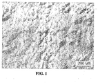
- FIG. 1 shows one typical textured surface morphology of gallium nitride film grown on a sapphire substrate at optimal growth temperature and NH 3 /HCl ratio.
- the specific optimized growth conditions for growth of this GaN surface included a growth temperature of 1030°C, an ammonia to hydrogen chloride ratio, NH 3 :HCl, of 30 and a growth rate of 116 ⁇ m/hr. As shown in FIG. 1 , the GaN surface produced under these optimized GaN growth conditions exhibited hillock surface morphology.
- FIG. 2 shows a pitted surface morphology of HVPE GaN film that is typical of GaN material that is grown under conditions of slightly lower temperature, or slightly higher ammonia flow (higher NH 3 :HCl ratio), or both slightly lower temperature and slightly higher ammonia flow (higher NH 3 :HCl ratio), than is employed in the optimal process conditions.
- the surface exhibits pits in this sub-optimal regime of lower temperature and/or higher ammonia flow rate than the optimal process conditions
- the GaN film exhibits single crystalline character and the extent of pitting is desirably at a high level, so that as much of the growth surface as possible is covered with pit formations.
- the pit-forming phase of the growth process of the present invention is desirably carried out to yield a pit density on the growth surface of the GaN material that is at least 100 pits/cm 2 of growth surface area, preferably being greater than 500 pits/cm 2 of growth surface area at the end of the pitted growth phase.
- the substrate can be removed to yield a freestanding GaN wafer blank.
- the freestanding GaN wafer blank then may be subjected to post-growth processing steps, such as lapping, polishing, and chemical mechanical polishing (CMP) to produce the finished GaN wafer, as more fully described in Xu et al. U.S. Patent 6,488,767 .
- CMP chemical mechanical polishing
- the surface morphology of the CMP-finished GaN wafer is related to the morphology of the wafer blank prior to processing.
- FIG. 3 is a differential interference contrast (DIC) optical microscope image of a CMP-finished GaN wafer.
- the starting as-grown wafer blank had a pit-free textured surface morphology, similar to the surface morphology shown in FIG. 1 .
- the CMP-finished wafer was very smooth and featureless.
- FIG. 4 is a differential interference contrast (DIC) microscope image of a pitted GaN wafer after lapping, mechanical polishing and CMP finishing. Even though the pits are completely removed during the mechanical polishing step, the CMP-finished wafer surface appears to have two regions, one of which is recessed slightly below the other. The shape and size of the recessed regions are very similar to the shape and size of the pits that were present during growth at the same cross-section. The recessed region corresponds to the material growth in the pits, in a growth direction along the facets of the pits and the other region corresponds to the material that is grown in a growth direction along the c-axis.
- DIC differential interference contrast
- the impurity concentration is higher for the material grown along the surface of the pits than in the material grown along the c-axis.
- the rate of chemical mechanical polishing of the respective materials is correspondingly slightly different, with the material grown with the growth direction along the facets of the pits having a higher removal rate than the material grown along the c-axis, leading to the observed indentation.
- Even the microscopic crystal growth direction inside the pits is along the facets of the pits, and the surface is still a c-axis surface after removing the pits by polish and CMP.
- the degree of indentation can be minimized by using a smaller grit diamond material in the mechanical polishing step prior to the CMP step, and shorter CMP processing time.
- FIG. 5 is a room-temperature total-intensity catholuminescence image of a GaN surface, as polished mechanically and finished with a CMP finishing process.
- FIG. 5 thus reflects a mapping of total room temperature catholuminescence intensity for a CMP-finished GaN wafer having a morphology similar to the wafer whose optical micrograph is shown in FIG. 4 .
- the surface has two regions that have different catholuminescent properties.
- the recessed area exhibited a high total CL intensity at room temperature.
- the crystalline defects (dislocations) in the material shown in FIG. 5 are observable in the CL mapping as dark spots corresponding to dislocations.
- the dislocations are concentrated near the center of the recessed area.
- the chemical mechanical polishing process also decorates the threading dislocations as pits that are observable by AFM.
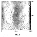
- FIG. 6 is an AFM image of a 50 micron x 50 micron area of a CMP-finished GaN wafer having a surface similar to that shown in FIG. 4 hereof and grown by a pitted surface growth process.
- the distribution of the crystal defects was not uniform, and the center region of the recessed area had a higher density of dislocations.
- the overall dislocation density was about 1 x 10 7 /cm 2 of GaN surface area, although many 10 micron x 10 micron areas of the surface have dislocation density below 5 x 10 6 /cm 2 . This dislocation distribution was associated with HVPE growth conditions yielding a pitted surface morphology.
- FIG. 7 is an AFM image of a 50 micron x 50 micron area of a CMP-finished GaN material with surface morphology similar to that of the GaN surface shown in FIG. 3 , and grown using a pit-free process.
- the distribution of the etch pits and dislocation density of the GaN surface was uniform, with an average dislocation density of the GaN surface on the order of about 1 x 10 7 dislocations/cm 2 .
- the average dislocation density of GaN films produced by conditions that yield pitted surface morphology i.e., films grown by a pit-forming growth process
- the average dislocation density of GaN films produced by conditions that yielded pit-free textured surface was approximately the same, the distribution of the dislocations was different in the two processes.
- the pit-forming growth process yielded films with randomly distributed low dislocation areas and high dislocation areas.
- the origin of this low dislocation density area morphology in the pit-forming growth process related to the fact that under pitted growth conditions, surface pits were formed during the growth of the GaN material.
- These pits were typically faceted pits in the shape of inverse hexagonal pyramids and occasionally inverse dodecagonal pyramids.
- the facets of the pits comprised typical ⁇ 11-22> and ⁇ 11-01> family planes.
- the growth rate on the c-plane (c-axis growth) and on the facets of the pits can differ from one another and can change differently in relation to one another with changes in the growth conditions.
- the pits Under conditions that promote higher growth rates in the c-axis direction than in the facet direction of the pits, the pits will grow larger and eventually cover the growth surface. When the growth conditions that have higher growth rate on the facets of the pits than on the c-plane are imposed, pits will be filled.
- the growth rate on the c-plane should be similar to or slightly greater than the growth rate on facets of the pits. Threading dislocations typically follow the growth direction, and thus the direction of the threading dislocations in the GaN film grown with pitted surface morphology will not be parallel to the c-axis, but rather, will have a tilt angle with respect to the average growth direction.
- dislocations concentrated near the center of the pits can sometimes disperse outwardly as the pits grow larger.
- FIG. 8 is a DIC optical image of a GaN surface after CMP and etching with hot phosphoric acid.
- the optical image shows the concentration of dislocations on the growth surface of the GaN material.
- the GaN material was grown under pitted growth morphology to a thickness of about 5 mm.
- the dislocations were decorated as etching pits and observed with the DIC microscope.
- the distribution of the pits was not uniform. Some areas had extremely low dislocation density ( ⁇ 1E5 cm -2 ), while other areas had moderately high dislocation density ( ⁇ 1E7 cm -2 ).
- the dislocations concentrated in the areas that constituted the center and certain edges of the pits during the growth process. Under pitting growth conditions, the dislocations did not continue to annihilate substantially, even when the GaN material was grown to a thickness of 5 mm.
- gallium nitride material is grown to produce a large area, uniformly low dislocation density gallium nitride material, e.g., in the form of a substrate article, such as a boule or single wafer body, by first concentrating the dislocations and then annihilating them in respective phases of the growth process.
- a substrate article such as a boule or single wafer body
- gallium nitride material is grown to produce a large area, uniformly low dislocation density gallium nitride material, e.g., in the form of a substrate article, such as a boule or single wafer body, by first concentrating the dislocations and then annihilating them in respective phases of the growth process.
- the pitted growth phase in which the GaN material is grown to form and develop pits in the growth surface, at least two microscopic growth directions exist, one along the c-axis and the other along the facets of the pits.
- the growth rates on the c-plane should be similar to
- the growth condition is changed in such manner that the growth rate on the facets of the pits is greater than the growth rate on the c-plane.
- the pits will grow smaller because of the higher growth rate on the facets of the pits.
- the threading dislocations in following the growth direction are thereby concentrated and annihilate with reduction of the pit size of the pits across the growth surface, i.e., the facets of the pits will eventually grow to meet in a single point due to faster growth rate on the facets than on the c-plane, so that the concentrated dislocations meeting one another either annihilate each other or merge into a single dislocation.
- FIGS. 9A-9E are a series of schematic illustrations showing the growth of a GaN substrate article according to one embodiment of the present invention, including provision of a substrate ( FIG. 9A ). Growth of GaN on such substrate is carried out under pitted growth conditions producing small pits in the GaN film on the substrate surface, with lines perpendicular to growth surface representing threading dislocations ( FIG. 9B ). Note that the angle of the dislocations is exaggerated to illustrate the phenomenon. The pit-forming growth is continued so that the pits in the GaN material grow larger and concentrate the dislocations in the material ( FIG. 9C ). Growth of the GaN material then is shifted to pit-filling growth conditions.
- the pits grow smaller, partially annihilating the dislocations, until pits are completely filled and all dislocations meet at the moment of pit closure, leaving a few dislocations remaining ( FIG. 9D ).
- the pit-filling growth step preferably is carried out until an essentially pit-free surface is produced.
- the growth of the GaN material then is continued to form the GaN material to a desired thickness, with the growth surface being constituted by substantially dislocation-free GaN in such further growth, to produce a large area, uniformly low dislocation density product GaN material ( FIG. 9E ).
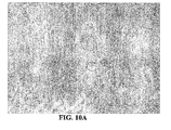
- FIGS. 10A-10B show differential interference contrast (DIC) optical microscope images ( FIG. 10A , top view of wafer obtained by focusing on the surface; FIG. 10B , image underneath the surface of the same area as the FIG. 10A view, by adjusting the focus of the microscope to the undersurface) of the defect distribution of a GaN wafer grown according to one embodiment of the present invention.
- DIC differential interference contrast
- the dislocations were decorated as etch pits by chemical mechanical polishing and hot phosphoric acid etching. Due to the subtle difference between material grown along c-axis and the material grown along the facets of the pits, a corresponding contrast between the two materials (c-axis material, and facet direction material) was observed under DIC. This allowed identification of the area under which growth along the facets of the pits (pit-filling) occurred, as circled in FIG. 10 . In one area, the dislocations were completely eliminated after the pit-filling, resulting in perfect crystalline character. In other areas, only one dislocation remained after pit closure. The dislocation density for the wafer was about 1 E6 cm -2 and the defects were uniformly distributed.
- the initial substrate for the growth of uniformly low dislocation density gallium nitride in accordance with the present invention may be of any suitable type, including, for example, gallium nitride, sapphire, silicon carbide, gallium arsenide, silicon, lithium gallate, lithium aluminate, lithium aluminum gallate, zinc oxide, diamond, spinel, magnesium oxide, etc. It will be appreciated that different substrates may require different substrate pretreatments prior to growth of gallium nitride in order to achieve high crystalline quality, as is readily determinable within the skill of the art based on the disclosure herein.
- the growth temperature, the growth rate, and the NH 3 :HCl ratio are controlled in the respective phases of the two-phase process to produce the desired large area, uniformly low dislocation density GaN material.
- constant temperature (1030°C, for example) and constant HCl flow to produce constant growth rate, e.g., a growth rate of 150 ⁇ m/hr
- increasing the NH 3 flow will change the GaN growth process from an optimal pit-filling growth condition that produces pit-free textured surface, to a pitted growth condition that produces pitted surface morphology.
- constant HCl and NH 3 flow producing a constant growth rate at a constant NH 3 /HCl ratio
- reducing the growth temperature will change the growth condition from an optimal pit-filling growth condition to a pitted growth condition.
- the reactor geometry of the specific GaN growth reactor that is employed for growing the GaN material in accordance with the process of the invention will affect the flows and local growth environments of the growth process. It therefore is important to systematically investigate the growth morphology as a function of the growth parameters, in order to identify the pitted growth conditions and the pit-filling growth conditions for a specific reactor employed in a given application of the present invention. Such determination is readily made within the skill of the art, as hereinabove described, utilizing optical micrographs, SEM and AFM techniques to characterize the surface in the pit-forming and pit-filling phases of the GaN growth process, to identify specific process conditions appropriate for forming the large area, uniformly low dislocation density GaN material.
- the respective growth conditions are carried out sequentially to produce uniformly low dislocation density gallium nitride as a large area, single-crystal material.
- the pitted growth step i.e., the growth of GaN under conditions serving to form pits and to concentrate dislocations at the bottoms of the pits in the material, is critical to the reduction of the overall dislocation density.
- the growth process is carried out so that the growth surface is covered with pits, so that the dislocations are swept to the bottoms of the pits and can be annihilated in the second growth step (pit-filling step).
- the first step of pitted growth it is preferable to conduct the first step of pitted growth so that greater than 50% of the growth surface is covered with pits, more preferably to have greater than 75% of the surface area covered with pits, and even more preferably to have greater than 90% of the growth surface covered with pits, prior to the second step of pit-filling growth.
- the reason for the.preference for high coverage of the pits on the growth surface is that growth along the c-axis (i.e., the area not covered with the pits) involves dislocations growing along the same direction, so that the dislocations have substantially reduced chance for annihilation and the final product correspondingly has higher dislocation density.
- the pitted growth process functions to concentrate the dislocations.
- the pit density is inversely proportional to the square of the pit size.
- the final dislocation density after the second pit-filling step depends on the density of pits, since not all dislocations in the pits will necessarily be annihilated.
- GaN GaN growth surface in the pitted growth phase
- growth under conditions favoring preferential growth in the facet direction of the pits, to form larger-sized pits at the end of the pitted growth phase, prior to conducting the second phase of pit-filling growth permits the achievement of large area, uniformly low dislocation density GaN.
- the average pit size of pits on the GaN surface prior to the pit-filling step preferably is greater than 25 ⁇ m, more preferably greater than 50 ⁇ m, and most preferably greater than 100 ⁇ m.
- Such pit size is the maximum diameter or transverse dimension of the pit measured at the growth surface, in the plane of such surface.
- the upper limit of pit size may be imposed by crystallographic factors, which at larger pit sizes increase the likelihood that polycrystalline formation within the pit will degrade rather than improve the crystalline character of the growing GaN material.
- the position of the pits on the GaN surface can be randomly distributed, produced stochastically by the pitted growth process under the corresponding pitted growth conditions. Alternatively, the position of the pits can be predetermined, by appropriate processing of the starting substrate.
- the starting substrate can alternatively be patterned to produce faceted growth morphology.
- a pitted (faceted) growth condition is used to produce facets.
- the growth rate along the c-axis is faster than the growth rate on the facets, producing a surface covered with facets.
- the dislocations are swept to the valley regions between the facets, but are not substantially annihilated.
- the growth rate on the facets is faster than the growth rate on the c-axis, so that the valleys between the facets are filled up, leading to the formation of a smooth c-axis growth material.
- the dislocations are confined and they either annihilate each other or merge into fewer dislocations.
- the first pitted growth phase and the second pit-filling phase may each be carried out in one or more steps, and the vapor phase growth process may be carried out with other process steps, other than first and second phase steps, e.g., intermediate process steps may be carried out between the first phase and second phase steps, as may be desired in a given application of the method of the invention.
- the thickness of the pitted or faceted growth layer should be thick enough to permit substantial concentration of the dislocations near the bottom of the pits or near valleys between the facets.
- the thicker the pitted layer the higher the surface coverage with dislocation-concentrating pits, thus the better the final product gallium nitride material.
- the pitted growth layer is preferably grown to a thickness greater than 50 ⁇ m, more preferably a thickness greater than 100 ⁇ m, and even more preferably a thickness greater than 200 ⁇ m.
- the growth condition is changed to a pit-filling condition, in which the growth rate on the facets is faster than the growth rate on the c-plane.
- the pit-filling conditions involve lower NH 3 flow (i.e., lower NH 3 /HCl ratio) than the pitted growth condition.
- the dislocations in the pits are substantially annihilated, resulting in uniformly low dislocation density GaN.
- the duration of the pit-filling growth should at a minimum allow the filling and closure of a majority of the pits, or otherwise achieve a desired low pit density, as appropriate to produce uniformly low dislocation density GaN.
- the duration of the pit-filling growth process necessary for fill of the pits is readily determinable by optical, SEM and AFM techniques as described herein.
- the pit-filling growth step is conducted until the pit density has been reduced to a level not exceeding 10 pits/cm 2 of the growth surface. More preferably, the pit-filling step is continued to form an essentially pit-free surface, e.g., having a pit density of 1 pit/cm 2 or less.
- the growth process is conducted in such manner as to produce a III-V nitride single crystal material having a totally pit-free surface.
- the thickness of the final c-plane growth should be such as to allow the material at the front surface after the GaN wafer forming steps to remain a uniformly c-plane growth material.
- the thickness of the complete c-plane growth after the pits are completely filled is advantageously at least 50 ⁇ m. More preferably, the thickness of the GaN material is greater than 200 ⁇ m, and most preferably such thickness is greater than 400 ⁇ m.
- the thickness of the c-plane growth may in part be determined such that wafer fabrication yields an upper surface that is all c-plane. If the c-plane growth is not carried out for a long enough period of time after pit closure, the surface of the finished wafer may contain recessed regions, similar to those shown in Figure 4 . If sufficient c-plane growth is carried out, a smooth, recess-free surface is produced, as shown in Figure 3 .
- Additional thickness may be required to reduce impurity concentration, reduce dislocation density or to enable angle lapping for off-cut wafers with the same crystalline orientation.
- Longer growth (>2mm) at the pit-filling conditions to produce a GaN ingot is advantageous, since under longer growth condition, the dislocations may further annihilate and the long ingot then can be sliced into multiple wafers of large area, uniformly low dislocation density and high quality, for subsequent device fabrication thereon to produce microelectronic and opto-electronic products.
- multiple cycles of pit-forming and pit-filling steps can be employed to further reduce dislocation density.
- Concerning the angle of growth of the III-V nitride material in the pits the general growth direction in the pits should be roughly c-axis growth but tilted.
- the process of the invention involving pitting growth serves to substantially reduce the susceptibility of the product III-V nitride material to cracking.
- the transition from pitted growth conditions to pit-filling growth conditions can be abrupt, gradual or multi-stepped.
- each phase of the pitted growth and pit-filling growth can involve more than one set of growth conditions.
- the pitted growth phase it may be advantageous to have a condition that produces high density of smaller pits at the beginning of the growth, followed by a condition to grow, coalesce and/or partly fill small pits to form larger pits at the end of the pitted growth phase.
- the pit-filling phase it may be advantageous to have a condition that fills the pits completely, followed by a condition that produces growth on the c-plane surface at a higher rate.
- the transition between different growth conditions may be gradual or ramped, so that the phases of pitted growth and pit-filling growth become less sharply demarcated from one another.
- the growth process of the invention may be carried out in multiple cycles of alternating pit growth and pit-filling growth steps (e.g., a first step of pit growth, followed by a second step of pit-filling growth, followed by a third step of pit growth, followed by a fourth step of pit-filling growth, optionally with additional pit growth and pit-filling growth steps in sequence).
- the density of such growth pits is less than 1 cm -2 . Excluding such growth pits, the GaN material has uniformly low dislocation density.
- the surface after CMP contains a recessed area of the type shown in FIG. 4 .
- the surface may still contain a recessed area of the type shown in FIG.4 .
- the recessed area typically has higher concentration of impurities such as oxygen or silicon.
- the distribution of the dislocations in the recessed area typically is not uniform. Excluding the recessed area, the surface has uniformly low dislocation density.
- the recessed area is less than 10% of the overall wafer surface area.
- the impurities in a semiconductor material affect the electric properties of the material. For example, it is well-established that silicon and oxygen act as shallow donors in GaN to produce n-type conductivity. Oxygen often is un-intentionally incorporated in GaN during HVPE growth because of gas source impurities and reactor leaks. Magnesium also may be introduced to the GaN material as an impurity species that acts as an acceptor in GaN, and with proper activation, produces p-type conductivity GaN material. Additionally, transition metals may be introduced to the GaN material to function as deep level acceptors to produce semi-insulating GaN, by compensating residual donor species in the GaN material.
- n-type conduction can be increased and controlled by intentionally introducing a silicon impurity from a silicon source such as silane or by introducing an oxygen-containing inpurity such as dioxygen in the gas stream that is fed to the GaN growth reactor.
- a silicon impurity from a silicon source such as silane
- an oxygen-containing inpurity such as dioxygen in the gas stream that is fed to the GaN growth reactor.
- the growth conditions that produce pitted growth morphology and pit-filling may be slightly different from those that are employed in the absence of such impurities being introduced, and as a result of the presence of such impurities, it may be necessary to correspondingly adjust the process conditions to most advantageously carry out doping in the pitted growth and pit filling phases of the two-stage process.
- the amount of impurities in the growth ambient and incorporation may be different during each stage of the process. Impurities when used can be introduced in the pitted growth step, or in the pit-filling step, or in both the pitted growth and the pit-filling steps.
- the growth of GaN on a substrate by the successive steps of pitted growth and pit-filling growth in accordance with the invention, produces a GaN wafer product.
- Two main types of wafer-forming processes can be utilized - ingot processes and single wafer processes.
- the grown GaN material is thick, e.g., forming an ingot with a length greater than about 2 mm
- a multi-wafer process is advantageously employed.
- the ingot is oriented, ground to a pre-determined size, e.g., ⁇ 5 cm ( ⁇ 2 inches) in diameter, and sliced into multiple wafers.
- the ingot as a bulk GaN material article which functions as a source body for production of multiple wafers, typically has a thickness of at least 1 mm, more preferably at least 5 mm, and most preferably at least 10 mm. After the multiple wafers are sliced from the ingot, the back and front main surfaces of the wafer are processed.
- the back side of the GaN wafer is lapped and/or polished, and the front side of the GaN wafer is lapped, polished and CMP-finished, to produce a GaN wafer ready for homoepitaxial growth.
- the wafers may have any suitable thickness.
- wafers may be formed having thicknesses in excess of 50 ⁇ m, 200 ⁇ m, or 500 ⁇ m, as necessary or desired for a specific application.
- Ingots may also be formed with homogeneous pit growth and pit-filling growth steps to produce bulk III-V nitride articles that are amenable to producing wafers of alternative orientations, e.g., a-plane wafers, m-plane wafers, etc., as sliced from the boule and finished into polished wafers.
- wafers of alternative orientations e.g., a-plane wafers, m-plane wafers, etc.
- the substrate for the GaN growth is not gallium nitride, and the foreign substrate (template) is removed prior to formation of the GaN wafer.
- the template removal can be carried out by any suitable means or method.
- the template removal may involve elimination of the template, removal of part or all of the template, or removal of all of the template and part of the GaN adjacent to the template.
- Specific techniques that may usefully be employed for such purpose include mechanical grinding, chemical etching, interfacial decomposition, interfacial fracturing, or any other means or method appropriate to the particular template.
- the heteroepitaxial substrate is removed in situ from the grown GaN material at a temperature in the vicinity of the growth temperature at the conclusion of the growth process, to yield a separated GaN substrate article of freestanding character.
- Such in situ removal produces a freestanding GaN wafer substrate having no thermal coefficient of expansion (TCE) defects therein, such as otherwise are produced when the heteroepitaxial structure including the grown GaN material and the foreign substrate are cooled to ambient (e.g., room) temperature.
- TCE thermal coefficient of expansion
- an in situ etching away of the foreign substrate at the growth temperature, or at a temperature in the vicinity of the growth temperature, e.g., within 100°C of the growth temperature, with a chemical etchant reagent effective for such purpose, is one approach for forming a high quality GaN substrate article in the single wafer process.
- the grown GaN then is sized appropriately, to a predetermined size, ⁇ 5 cm ( ⁇ 2 inches) diameter, for example, by an appropriate technique, such as for example mechanical grinding, or sandblasting, or laser cutting. Subsequently, the back side of the grown GaN is lapped and/or polished, and the front side of the grown GaN is lapped, polished and CMP-finished to produce a GaN wafer ready for homoepitaxial growth. Since the front side of the grown GaN has higher quality than the back side of the grown GaN, the material removal from the front side is desirably minimized.
- Lapping and polishing of the front side is utilized mainly for the purpose of achieving a flat wafer conformation, and lapping of the backside is utilized primarily to achieve a desirable GaN wafer thickness.
- the front side of the GaN wafer has uniformly low dislocation density.
- the back side may have higher dislocation density than the front side, and the distribution of the dislocation density may be not uniform at the backside.
- the chemical mechanical polish (CMP) can be carried out using any suitable CMP formulation and CMP process.
- the CMP rate is slightly higher in the recessed area where the material was grown in the direction along the facets of the pits on the growth surface and has higher impurity concentration.
- the CMP polished surface is smooth, with surface roughness (RMS) less than 1 nm as measured by AFM in the 10 x 10 ⁇ m area.
- the wafer can be processed in such way that the surface of the wafer is parallel to the c-plane of the GaN crystal.
- the surface of the wafer can be at a small angle (e.g., ⁇ 10°) with respect the crystalline c-plane.
- Such surface is called a vicinal surface.
- Such vicinal GaN surface is advantageous for homoepitaxial growth.
- GaN wafers produced by the methods disclosed herein are of high quality for device fabrication applications, of large area, and have a low density of dislocations, with the dislocations uniformly distributed across the large area wafer surface.
- the density of the dislocations on the wafer surface typically does not exceed about 1E6 cm -2 .
- the prior art has produced either low dislocation density but small area GaN (which is unable to be grown to larger size), or alternatively large area GaN having non-uniformly distributed defects across the wafer. As discussed herein in the Background section hereof, the prior art has been unable to achieve the combination of large area single crystal growth of GaN and the provision of a low dislocation density that is uniformly low across the large area of the GaN substrate.
- III-V nitride material produced in accordance with the present invention is formed with at least one surface having uniformly low dislocation density.
- the III-V nitride material may be grown so that both main surfaces of the material have uniformly low dislocation density, or the III-V nitride material may be grown so that one of such main surfaces of the material has uniformly low dislocation density while the other main surface may have high and/or non-uniform distribution of the dislocations, with dislocation density progressively decreasing from the latter (e.g., bottom) surface to the former (e.g., top) surface.
- the III-V nitride material of the invention has at least one large area surface with uniformly low dislocation density.
- GaN wafers produced in accordance with the present invention can be utilized as a substrate for fabrication of a wide variety of electronic and opto-electronic devices and integrated circuitry products.
- Electronic device structures may therefore include the large area, uniformly low dislocation density GaN wafer produced in accordance with the invention, on which is fabricated a device, such as for example a laser diode, a light-emitting diode, or a high electron mobility transistor, as well as integrated circuitry including such GaN wafers, and GaN wafers of such type having at least one epitaxial layer thereon, which may be homoepitaxial or heteroepitaxial in character, depending on the specific application and end use of the GaN wafer-based product.
- a device such as for example a laser diode, a light-emitting diode, or a high electron mobility transistor
- integrated circuitry including such GaN wafers and GaN wafers of such type having at least one epitaxial layer thereon, which may be homoepitaxial or
- the present invention represents a significant improvement over the prior art, in providing high-performance gallium nitride substrates suitable for fabrication of microelectronic and opto-electronic devices.
- the growth temperature was 1010°C
- the NH 3 /HCl ratio was 17
- the growth rate was about 160 ⁇ m/hr
- the thickness of the grown film was about 320 ⁇ m.
- the growth temperature was raised to 1030°C, and the NH 3 /HCl ratio was reduced to 8.6, and growth was continued until the thickness of the second stage GaN material was about 640 ⁇ m.
- the sapphire substrate was removed from the thick GaN film.
- the GaN wafer blank was first ground about its edge by mechanical means.
- the GaN wafer had two surfaces.
- the surface constituting the growth surface was gallium-terminated.
- the side that was attached to the sapphire substrate was the nitrogen-terminated side.
- the gallium-side of the wafer was first lapped with coarse diamond slurry on a lap machine, and then polished with a fine diamond slurry on a polish pad.
- the front (gallium-side) was finished with a chemical mechanical polish process using a mixture of colloidal silica and diluted hydrochloric acid.
- the back side was lapped and polished.
- FIG. 11 is a photograph of the two-sided polished gallium nitride wafer produced by the foregoing process.
- the diameter of the wafer was 5 ⁇ 8 cm (2.3 inches).
- a piece of the wafer from the uniformly grown area of the gallium-terminated surface was polished by a CMP process and etched in hot phosphoric acid to determine its dislocation density.
- the CMP process and hot phosphoric acid etching decorated the dislocations as etch pits.
- FIG. 12 shows a differential interference contrast (DIC) microscope image of the resultantly etched surface. As shown, the etch pits were visible under the microscope. The etch pit density for the sample was 5.5E5 cm -2 .
- DIC differential interference contrast
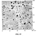
- FIG. 13 shows a 100 x 100 ⁇ m 2 AFM scan of the hot phosphoric acid-etched GaN wafer surface.
- the etch pit density for the image was 8.5E5 cm -2 , in good agreement with the etch pit density counted using the DIC optical microscope. Examination of the entire etched wafer under the microscope showed that the etch pits were uniformly distributed across the wafer surface.
- This example illustrates the growth of uniformly low dislocation density, large area gallium nitride wafer, produced by the method of the present invention.
- the two-step HVPE GaN growth process was carried out to grow a relatively long GaN ingot.
- the growth temperature was 1010°C
- the NH 3 /HCl ratio was 17
- the growth rate was about 160 ⁇ m/hr
- the thickness of the grown film was about 320 ⁇ m.
- the growth temperature was raised to 1030°C, and the NH 3 /HCl ratio was reduced to 12.9. Growth of the GaN material was continued until the length of the ingot was 3.2 mm.
- the ingot after its formation was processed into multiple wafers by slicing and subsequent lap, polish and chemical mechanical polish steps as in Example 1. Similar two-step HVPE GaN growth processes were carried out to grow GaN ingots having lengths on the order of 10 mm.
- III-V nitride material produced by the process of the invention is usefully employed for manufacture of microelectronic and optoelectronic devices, such as light-emitting diodes, laser diodes, opto-electronic sensors, opto-electronic switches, high electron mobility transistors, and the like.
- the III-V nitride material can be single crystal GaN, as employed in the form of a wafer or other substrate article.
Landscapes
- Chemical & Material Sciences (AREA)
- Organic Chemistry (AREA)
- Engineering & Computer Science (AREA)
- Crystallography & Structural Chemistry (AREA)
- Materials Engineering (AREA)
- Metallurgy (AREA)
- Inorganic Chemistry (AREA)
- General Chemical & Material Sciences (AREA)
- Chemical Kinetics & Catalysis (AREA)
- Crystals, And After-Treatments Of Crystals (AREA)
- Chemical Vapour Deposition (AREA)
- Light Receiving Elements (AREA)
- Led Devices (AREA)
- Semiconductor Lasers (AREA)
- Physical Vapour Deposition (AREA)
Applications Claiming Priority (2)
| Application Number | Priority Date | Filing Date | Title |
|---|---|---|---|
| US10/712,351 US7323256B2 (en) | 2003-11-13 | 2003-11-13 | Large area, uniformly low dislocation density GaN substrate and process for making the same |
| EP04811296A EP1682701B1 (en) | 2003-11-13 | 2004-11-12 | LARGE AREA, UNIFORMLY LOW DISLOCATION DENSITY GaN SUBSTRATE AND PROCESS FOR MAKING THE SAME |
Related Parent Applications (2)
| Application Number | Title | Priority Date | Filing Date |
|---|---|---|---|
| EP04811296A Division EP1682701B1 (en) | 2003-11-13 | 2004-11-12 | LARGE AREA, UNIFORMLY LOW DISLOCATION DENSITY GaN SUBSTRATE AND PROCESS FOR MAKING THE SAME |
| EP04811296.5 Division | 2004-11-12 |
Publications (2)
| Publication Number | Publication Date |
|---|---|
| EP2267190A1 EP2267190A1 (en) | 2010-12-29 |
| EP2267190B1 true EP2267190B1 (en) | 2015-08-12 |
Family
ID=34573533
Family Applications (2)
| Application Number | Title | Priority Date | Filing Date |
|---|---|---|---|
| EP04811296A Active EP1682701B1 (en) | 2003-11-13 | 2004-11-12 | LARGE AREA, UNIFORMLY LOW DISLOCATION DENSITY GaN SUBSTRATE AND PROCESS FOR MAKING THE SAME |
| EP10010831.5A Active EP2267190B1 (en) | 2003-11-13 | 2004-11-12 | Large area, uniformly low dislocation density gan substrate and process for making the same |
Family Applications Before (1)
| Application Number | Title | Priority Date | Filing Date |
|---|---|---|---|
| EP04811296A Active EP1682701B1 (en) | 2003-11-13 | 2004-11-12 | LARGE AREA, UNIFORMLY LOW DISLOCATION DENSITY GaN SUBSTRATE AND PROCESS FOR MAKING THE SAME |
Country Status (10)
| Country | Link |
|---|---|
| US (4) | US7323256B2 (ja) |
| EP (2) | EP1682701B1 (ja) |
| JP (3) | JP4741506B2 (ja) |
| KR (1) | KR101119728B1 (ja) |
| CN (1) | CN100577894C (ja) |
| AT (1) | ATE483834T1 (ja) |
| CA (1) | CA2544878A1 (ja) |
| DE (1) | DE602004029486D1 (ja) |
| PL (1) | PL1682701T3 (ja) |
| WO (1) | WO2005050709A2 (ja) |
Cited By (1)
| Publication number | Priority date | Publication date | Assignee | Title |
|---|---|---|---|---|
| US9293667B2 (en) | 2010-08-19 | 2016-03-22 | Soraa, Inc. | System and method for selected pump LEDs with multiple phosphors |
Families Citing this family (115)
| Publication number | Priority date | Publication date | Assignee | Title |
|---|---|---|---|---|
| US6488767B1 (en) * | 2001-06-08 | 2002-12-03 | Advanced Technology Materials, Inc. | High surface quality GaN wafer and method of fabricating same |
| US7638346B2 (en) * | 2001-12-24 | 2009-12-29 | Crystal Is, Inc. | Nitride semiconductor heterostructures and related methods |
| US20060005763A1 (en) * | 2001-12-24 | 2006-01-12 | Crystal Is, Inc. | Method and apparatus for producing large, single-crystals of aluminum nitride |
| US8545629B2 (en) | 2001-12-24 | 2013-10-01 | Crystal Is, Inc. | Method and apparatus for producing large, single-crystals of aluminum nitride |
| US7125453B2 (en) * | 2002-01-31 | 2006-10-24 | General Electric Company | High temperature high pressure capsule for processing materials in supercritical fluids |
| US7063741B2 (en) * | 2002-03-27 | 2006-06-20 | General Electric Company | High pressure high temperature growth of crystalline group III metal nitrides |
| US7323256B2 (en) * | 2003-11-13 | 2008-01-29 | Cree, Inc. | Large area, uniformly low dislocation density GaN substrate and process for making the same |
| US7118813B2 (en) | 2003-11-14 | 2006-10-10 | Cree, Inc. | Vicinal gallium nitride substrate for high quality homoepitaxy |
| US8120139B2 (en) * | 2003-12-05 | 2012-02-21 | International Rectifier Corporation | Void isolated III-nitride device |
| JP2005209803A (ja) * | 2004-01-21 | 2005-08-04 | Sumitomo Electric Ind Ltd | GaN結晶基板の製造方法 |
| JP4720125B2 (ja) * | 2004-08-10 | 2011-07-13 | 日立電線株式会社 | Iii−v族窒化物系半導体基板及びその製造方法並びにiii−v族窒化物系半導体 |
| FI20045482A0 (fi) * | 2004-12-14 | 2004-12-14 | Optogan Oy | Matalamman dislokaatiotiheyden omaava puolijohdesubstraatti, ja menetelmä sen valmistamiseksi |
| DE102005003884A1 (de) * | 2005-01-24 | 2006-08-03 | Forschungsverbund Berlin E.V. | Verfahren zur Herstellung von c-plane orientierten GaN-oder AlxGa1-xN-Substraten |
| US7704324B2 (en) * | 2005-01-25 | 2010-04-27 | General Electric Company | Apparatus for processing materials in supercritical fluids and methods thereof |
| US7919815B1 (en) * | 2005-02-24 | 2011-04-05 | Saint-Gobain Ceramics & Plastics, Inc. | Spinel wafers and methods of preparation |
| JP4849296B2 (ja) | 2005-04-11 | 2012-01-11 | 日立電線株式会社 | GaN基板 |
| JP4792802B2 (ja) * | 2005-04-26 | 2011-10-12 | 住友電気工業株式会社 | Iii族窒化物結晶の表面処理方法 |
| DE112006001847B4 (de) | 2005-07-11 | 2011-02-17 | Cree, Inc. | Ausrichtung von Laserdioden auf fehlgeschnittenen Substraten |
| KR101220826B1 (ko) * | 2005-11-22 | 2013-01-10 | 삼성코닝정밀소재 주식회사 | 질화갈륨 단결정 후막의 제조방법 |
| WO2007062250A2 (en) | 2005-11-28 | 2007-05-31 | Crystal Is, Inc. | Large aluminum nitride crystals with reduced defects and methods of making them |
| CN101331249B (zh) * | 2005-12-02 | 2012-12-19 | 晶体公司 | 掺杂的氮化铝晶体及其制造方法 |
| US8435879B2 (en) * | 2005-12-12 | 2013-05-07 | Kyma Technologies, Inc. | Method for making group III nitride articles |
| JP2007161536A (ja) * | 2005-12-14 | 2007-06-28 | Sumitomo Electric Ind Ltd | AlxGayIn1−x−yN結晶基板、半導体デバイスおよびその製造方法 |
| US8039412B2 (en) * | 2005-12-20 | 2011-10-18 | Momentive Performance Materials Inc. | Crystalline composition, device, and associated method |
| US7942970B2 (en) * | 2005-12-20 | 2011-05-17 | Momentive Performance Materials Inc. | Apparatus for making crystalline composition |
| US7935382B2 (en) * | 2005-12-20 | 2011-05-03 | Momentive Performance Materials, Inc. | Method for making crystalline composition |
| EP1972702B1 (en) * | 2006-01-12 | 2013-09-25 | Sumitomo Electric Industries, Ltd. | Method for manufacturing aluminum nitride crystal, aluminum nitride crystal, aluminum nitride crystal substrate and semiconductor device |
| US9034103B2 (en) | 2006-03-30 | 2015-05-19 | Crystal Is, Inc. | Aluminum nitride bulk crystals having high transparency to ultraviolet light and methods of forming them |
| EP2007933B1 (en) * | 2006-03-30 | 2017-05-10 | Crystal Is, Inc. | Methods for controllable doping of aluminum nitride bulk crystals |
| US9518340B2 (en) | 2006-04-07 | 2016-12-13 | Sixpoint Materials, Inc. | Method of growing group III nitride crystals |
| US9543393B2 (en) | 2006-04-07 | 2017-01-10 | Sixpoint Materials, Inc. | Group III nitride wafer and its production method |
| WO2007117689A2 (en) * | 2006-04-07 | 2007-10-18 | The Regents Of The University Of California | Growing large surface area gallium nitride crystals |
| WO2007145873A2 (en) * | 2006-06-05 | 2007-12-21 | Cohen Philip I | Growth of low dislocation density group-iii nitrides and related thin-film structures |
| CN101473075B (zh) * | 2006-06-20 | 2012-09-05 | 住友电气工业株式会社 | AlxGa1-xN晶体的生长方法和AlxGa1-xN晶体衬底 |
| JP5125098B2 (ja) * | 2006-12-26 | 2013-01-23 | 信越半導体株式会社 | 窒化物半導体自立基板の製造方法 |
| WO2008088838A1 (en) | 2007-01-17 | 2008-07-24 | Crystal Is, Inc. | Defect reduction in seeded aluminum nitride crystal growth |
| US9771666B2 (en) | 2007-01-17 | 2017-09-26 | Crystal Is, Inc. | Defect reduction in seeded aluminum nitride crystal growth |
| US8080833B2 (en) | 2007-01-26 | 2011-12-20 | Crystal Is, Inc. | Thick pseudomorphic nitride epitaxial layers |
| WO2008094464A2 (en) * | 2007-01-26 | 2008-08-07 | Crystal Is, Inc. | Thick pseudomorphic nitride epitaxial layers |
| WO2008143166A1 (ja) * | 2007-05-17 | 2008-11-27 | Mitsubishi Chemical Corporation | Iii族窒化物半導体結晶の製造方法、iii族窒化物半導体基板および半導体発光デバイス |
| US8088220B2 (en) * | 2007-05-24 | 2012-01-03 | Crystal Is, Inc. | Deep-eutectic melt growth of nitride crystals |
| JP2008300540A (ja) * | 2007-05-30 | 2008-12-11 | Sumitomo Electric Ind Ltd | 半導体発光素子の製造方法 |
| DE102007026298A1 (de) * | 2007-06-06 | 2008-12-11 | Freiberger Compound Materials Gmbh | Anordnung und Verfahren zur Herstellung eines Kristalls aus der Schmelze eines Rohmaterials sowie Einkristall |
| TW200905730A (en) * | 2007-07-23 | 2009-02-01 | Ind Tech Res Inst | Method for forming a microcrystalline silicon film |
| JP5493861B2 (ja) * | 2007-10-09 | 2014-05-14 | 株式会社リコー | Iii族窒化物結晶基板の製造方法 |
| CN100575565C (zh) * | 2007-11-09 | 2009-12-30 | 中国科学院上海光学精密机械研究所 | 在铝酸锂晶片表面低温制备氮化铝薄膜的方法 |
| JP5018423B2 (ja) | 2007-11-20 | 2012-09-05 | 住友電気工業株式会社 | Iii族窒化物半導体結晶基板および半導体デバイス |
| JP2009137777A (ja) * | 2007-12-04 | 2009-06-25 | Sumitomo Electric Ind Ltd | AlN結晶およびその成長方法 |
| US20090229666A1 (en) * | 2008-03-14 | 2009-09-17 | Jason Stephan Corneille | Smoothing a metallic substrate for a solar cell |
| US8546172B2 (en) | 2008-01-18 | 2013-10-01 | Miasole | Laser polishing of a back contact of a solar cell |
| US8536054B2 (en) | 2008-01-18 | 2013-09-17 | Miasole | Laser polishing of a solar cell substrate |
| US8586398B2 (en) | 2008-01-18 | 2013-11-19 | Miasole | Sodium-incorporation in solar cell substrates and contacts |
| JP5560528B2 (ja) | 2008-01-28 | 2014-07-30 | 住友電気工業株式会社 | Iii族窒化物単結晶インゴットの製造方法、及びiii族窒化物単結晶基板の製造方法 |
| JP2009280482A (ja) * | 2008-04-25 | 2009-12-03 | Sumitomo Electric Ind Ltd | Iii族窒化物単結晶自立基板およびそれを用いた半導体デバイスの製造方法 |
| EP2314738A4 (en) * | 2008-07-01 | 2014-08-13 | Sumitomo Electric Industries | PROCESS FOR PREPARING AN ALXGA (1-X) N-CRYSTAL, ALXGA (1-X) N-CRYSTAL AND OPTICS |
| US20100117118A1 (en) * | 2008-08-07 | 2010-05-13 | Dabiran Amir M | High electron mobility heterojunction device |
| US20100072484A1 (en) * | 2008-09-23 | 2010-03-25 | Triquint Semiconductor, Inc. | Heteroepitaxial gallium nitride-based device formed on an off-cut substrate |
| US20110203514A1 (en) * | 2008-11-07 | 2011-08-25 | The Regents Of The University Of California | Novel vessel designs and relative placements of the source material and seed crystals with respect to the vessel for the ammonothermal growth of group-iii nitride crystals |
| US8878230B2 (en) * | 2010-03-11 | 2014-11-04 | Soraa, Inc. | Semi-insulating group III metal nitride and method of manufacture |
| CA2755122C (en) | 2009-03-13 | 2016-05-31 | Saint-Gobain Ceramics & Plastics, Inc. | Chemical mechanical planarization using nanodiamond |
| JP4758492B2 (ja) * | 2009-03-24 | 2011-08-31 | トヨタ自動車株式会社 | 単結晶の欠陥密度測定方法 |
| US8096671B1 (en) | 2009-04-06 | 2012-01-17 | Nmera, Llc | Light emitting diode illumination system |
| US20100314551A1 (en) * | 2009-06-11 | 2010-12-16 | Bettles Timothy J | In-line Fluid Treatment by UV Radiation |
| US8133803B2 (en) * | 2009-06-23 | 2012-03-13 | Academia Sinica | Method for fabricating semiconductor substrates and semiconductor devices |
| CN101958236B (zh) * | 2009-07-20 | 2012-12-19 | 上海半导体照明工程技术研究中心 | 一种半导体衬底及其制备方法 |
| US8344420B1 (en) | 2009-07-24 | 2013-01-01 | Triquint Semiconductor, Inc. | Enhancement-mode gallium nitride high electron mobility transistor |
| US8933644B2 (en) | 2009-09-18 | 2015-01-13 | Soraa, Inc. | LED lamps with improved quality of light |
| DE102009055667A1 (de) * | 2009-11-25 | 2011-03-31 | Siltronic Ag | Verfahren zur Herstellung einer Scheibe bestehend aus Galliumnitrid |
| WO2011072014A1 (en) * | 2009-12-08 | 2011-06-16 | Lehigh Univeristy | THERMOELECTRIC MATERIALS BASED ON SINGLE CRYSTAL AlInN-GaN GROWN BY METALORGANIC VAPOR PHASE EPITAXY |
| US10147850B1 (en) | 2010-02-03 | 2018-12-04 | Soraa, Inc. | System and method for providing color light sources in proximity to predetermined wavelength conversion structures |
| US8740413B1 (en) | 2010-02-03 | 2014-06-03 | Soraa, Inc. | System and method for providing color light sources in proximity to predetermined wavelength conversion structures |
| US8905588B2 (en) | 2010-02-03 | 2014-12-09 | Sorra, Inc. | System and method for providing color light sources in proximity to predetermined wavelength conversion structures |
| TWI440074B (zh) * | 2010-04-02 | 2014-06-01 | Univ Nat Chiao Tung | 一種在三族氮化物磊晶過程中降低缺陷產生的方法 |
| JP5806734B2 (ja) | 2010-06-30 | 2015-11-10 | クリスタル アイエス, インコーポレーテッドCrystal Is, Inc. | 熱勾配制御による窒化アルミニウム大単結晶成長 |
| JP5714250B2 (ja) * | 2010-07-14 | 2015-05-07 | 住友電工デバイス・イノベーション株式会社 | 半導体装置の製造方法 |
| TW201228032A (en) * | 2010-10-26 | 2012-07-01 | Univ California | Vicinal semipolar III-nitride substrates to compensate tilt of relaxed hetero-epitaxial layers |
| CN103190041A (zh) | 2010-10-26 | 2013-07-03 | 加利福尼亚大学董事会 | 通过基底和外延层图案化限制在iii-氮化物异质结构中的应变松弛 |
| TWI467635B (zh) * | 2011-02-17 | 2015-01-01 | Soitec Silicon On Insulator | 凹孔缺陷縮減之三五族半導體構造及形成此等構造之方法 |
| DE102011012925A1 (de) * | 2011-03-03 | 2012-09-06 | Osram Opto Semiconductors Gmbh | Verfahren zur Herstellung eines optoelektronischen Halbleiterchips |
| FR2977260B1 (fr) * | 2011-06-30 | 2013-07-19 | Soitec Silicon On Insulator | Procede de fabrication d'une couche epitaxiale epaisse de nitrure de gallium sur un substrat de silicium ou analogue et couche obtenue par ledit procede |
| US8962359B2 (en) | 2011-07-19 | 2015-02-24 | Crystal Is, Inc. | Photon extraction from nitride ultraviolet light-emitting devices |
| WO2013089417A1 (en) | 2011-12-14 | 2013-06-20 | Seoul Opto Device Co., Ltd. | Semiconductor device and method of fabricating the same |
| WO2013089459A1 (en) * | 2011-12-14 | 2013-06-20 | Seoul Opto Device Co., Ltd. | Semiconductor device and method of fabricating the same |
| TWI528580B (zh) | 2012-03-30 | 2016-04-01 | 聖戈班晶體探測器公司 | 形成獨立式半導體晶圓之方法 |
| JP2013214686A (ja) * | 2012-04-04 | 2013-10-17 | Furukawa Co Ltd | Iii族窒化物半導体層およびiii族窒化物半導体層の製造方法 |
| KR101369967B1 (ko) * | 2012-04-12 | 2014-03-06 | 주식회사 루미스탈 | 휨이 없는 질화갈륨 자립기판 제조 방법 |
| JP6169704B2 (ja) | 2012-09-25 | 2017-07-26 | シックスポイント マテリアルズ, インコーポレイテッド | Iii族窒化物結晶を成長させる方法 |
| EP2900850B1 (en) | 2012-09-26 | 2018-11-14 | SixPoint Materials, Inc. | Fabrication method of group iii nitride wafers and testing method thereof |
| JP6322890B2 (ja) | 2013-02-18 | 2018-05-16 | 住友電気工業株式会社 | Iii族窒化物複合基板およびその製造方法、ならびにiii族窒化物半導体デバイスの製造方法 |
| WO2014057748A1 (ja) | 2012-10-12 | 2014-04-17 | 住友電気工業株式会社 | Iii族窒化物複合基板およびその製造方法、ならびにiii族窒化物半導体デバイスの製造方法 |
| WO2014123171A1 (ja) * | 2013-02-08 | 2014-08-14 | 並木精密宝石株式会社 | GaN基板及びGaN基板の製造方法 |
| WO2014125688A1 (ja) | 2013-02-18 | 2014-08-21 | 住友電気工業株式会社 | Iii族窒化物複合基板およびその製造方法、積層iii族窒化物複合基板、ならびにiii族窒化物半導体デバイスおよびその製造方法 |
| US20150280057A1 (en) | 2013-03-15 | 2015-10-01 | James R. Grandusky | Methods of forming planar contacts to pseudomorphic electronic and optoelectronic devices |
| CN103367209B (zh) * | 2013-07-26 | 2015-11-25 | 东莞市中镓半导体科技有限公司 | 一种液体辅助激光剥离方法 |
| US9574287B2 (en) * | 2013-09-26 | 2017-02-21 | Globalfoundries Inc. | Gallium nitride material and device deposition on graphene terminated wafer and method of forming the same |
| JP6262561B2 (ja) * | 2014-02-19 | 2018-01-17 | 古河機械金属株式会社 | Iii族窒化物半導体基板の評価方法 |
| JP6497886B2 (ja) * | 2014-10-03 | 2019-04-10 | 古河機械金属株式会社 | 自立基板、及び、自立基板の製造方法 |
| CN104911713A (zh) * | 2015-03-16 | 2015-09-16 | 中国电子科技集团公司第五十五研究所 | 一种利用氢气原位刻蚀提高氮化铝晶体质量的方法 |
| DE102015205104A1 (de) | 2015-03-20 | 2016-09-22 | Freiberger Compound Materials Gmbh | Züchtung von A-B Kristallen ohne Kristallgitter-Krümmung |
| JP6688109B2 (ja) * | 2016-02-25 | 2020-04-28 | 日本碍子株式会社 | 面発光素子、外部共振器型垂直面発光レーザー、および面発光素子の製造方法 |
| WO2017181167A1 (en) * | 2016-04-15 | 2017-10-19 | Massachusetts Institute Of Technology | Gan devices fabricated via wafer bonding |
| EP3516002B1 (en) | 2016-09-23 | 2022-01-05 | Saint-Gobain Ceramics & Plastics, Inc. | Chemical mechanical planarization slurry and method for forming same |
| US10497562B1 (en) * | 2018-05-29 | 2019-12-03 | Industry-University Cooperation Foundation Hanyang University | Method for manufacturing gallium nitride substrate using the hydride vapor phase epitaxy |
| JP6959190B2 (ja) | 2018-07-24 | 2021-11-02 | 旭化成エレクトロニクス株式会社 | 学習処理装置、学習処理方法、化合物半導体の製造方法およびプログラム |
| JP7106217B2 (ja) * | 2018-08-22 | 2022-07-26 | 株式会社ディスコ | ファセット領域の検出方法及び検出装置 |
| JP7326759B2 (ja) * | 2019-02-06 | 2023-08-16 | 三菱ケミカル株式会社 | GaN単結晶製造方法 |
| RU2714304C1 (ru) * | 2019-06-03 | 2020-02-14 | Федеральное государственное бюджетное образовательное учреждение высшего образования "ОРЛОВСКИЙ ГОСУДАРСТВЕННЫЙ УНИВЕРСИТЕТ имени И.С. ТУРГЕНЕВА" (ОГУ им. И.С. Тургенева) | Способ определения индексов направления дислокаций |
| CN112287543A (zh) * | 2020-10-28 | 2021-01-29 | 华天科技(西安)有限公司 | 一种氮化镓晶圆生产工艺参数设计方法 |
| US11638470B2 (en) | 2021-01-12 | 2023-05-02 | Arash Kani | Gallium nitride gemstones |
| CN112820636B (zh) * | 2021-01-14 | 2024-01-16 | 镓特半导体科技(上海)有限公司 | 半导体结构、自支撑氮化镓层及其制备方法 |
| CN112397571B (zh) | 2021-01-18 | 2021-04-23 | 苏州纳维科技有限公司 | 一种氮化镓衬底及半导体复合衬底 |
| CN112899783B (zh) * | 2021-01-18 | 2022-06-07 | 上海玺唐半导体科技有限公司 | 一种常压hvpe制作珊瑚状多晶氮化镓晶体的方法 |
| CN114242859B (zh) * | 2021-11-30 | 2023-05-02 | 福建兆元光电有限公司 | 一种Micro LED外延片制备方法 |
| WO2023182211A1 (ja) * | 2022-03-25 | 2023-09-28 | 東ソー株式会社 | 窒化ガリウム焼結体及びその製造方法 |
| WO2024095449A1 (ja) * | 2022-11-04 | 2024-05-10 | 住友電気工業株式会社 | 窒化ガリウム単結晶基板およびその製造方法 |
Family Cites Families (47)
| Publication number | Priority date | Publication date | Assignee | Title |
|---|---|---|---|---|
| US3462320A (en) * | 1966-11-21 | 1969-08-19 | Bell Telephone Labor Inc | Solution growth of nitrogen doped gallium phosphide |
| US3615205A (en) * | 1968-10-14 | 1971-10-26 | Ibm | Method for the synthesis and growth of high purity iii{14 v semiconductor compositions in bulk |
| US3628998A (en) * | 1969-09-23 | 1971-12-21 | Ibm | Method for growth of a mixed crystal with controlled composition |
| US5064497A (en) * | 1990-03-09 | 1991-11-12 | At&T Bell Laboratories | Crystal growth method and apparatus |
| PL173917B1 (pl) * | 1993-08-10 | 1998-05-29 | Ct Badan Wysokocisnieniowych P | Sposób wytwarzania krystalicznej struktury wielowarstwowej |
| US5679152A (en) | 1994-01-27 | 1997-10-21 | Advanced Technology Materials, Inc. | Method of making a single crystals Ga*N article |
| US6440823B1 (en) * | 1994-01-27 | 2002-08-27 | Advanced Technology Materials, Inc. | Low defect density (Ga, Al, In)N and HVPE process for making same |
| DE19640594B4 (de) * | 1996-10-01 | 2016-08-04 | Osram Gmbh | Bauelement |
| JPH11191657A (ja) | 1997-04-11 | 1999-07-13 | Nichia Chem Ind Ltd | 窒化物半導体の成長方法及び窒化物半導体素子 |
| DE69834092T2 (de) * | 1997-12-02 | 2006-09-21 | Ciba Speciality Chemicals Holding Inc. | Polyolefinmaterialien mit verbesserter Oberflächenhaltbarkeit und Verfahren zu ihrer Herstellung durch Strahlung |
| US6086673A (en) * | 1998-04-02 | 2000-07-11 | Massachusetts Institute Of Technology | Process for producing high-quality III-V nitride substrates |
| TW417315B (en) * | 1998-06-18 | 2001-01-01 | Sumitomo Electric Industries | GaN single crystal substrate and its manufacture method of the same |
| JP4005701B2 (ja) * | 1998-06-24 | 2007-11-14 | シャープ株式会社 | 窒素化合物半導体膜の形成方法および窒素化合物半導体素子 |
| JP3896718B2 (ja) | 1999-03-02 | 2007-03-22 | 日亜化学工業株式会社 | 窒化物半導体 |
| JP2000337830A (ja) | 1999-05-27 | 2000-12-08 | Kawasaki Steel Corp | コイル形状の測定方法及び装置 |
| JP2000357820A (ja) * | 1999-06-15 | 2000-12-26 | Pioneer Electronic Corp | 窒化ガリウム系半導体発光素子及びその製造方法 |
| JP4145437B2 (ja) * | 1999-09-28 | 2008-09-03 | 住友電気工業株式会社 | 単結晶GaNの結晶成長方法及び単結晶GaN基板の製造方法と単結晶GaN基板 |
| JP2001122693A (ja) | 1999-10-22 | 2001-05-08 | Nec Corp | 結晶成長用下地基板およびこれを用いた基板の製造方法 |
| JP3568112B2 (ja) * | 1999-12-27 | 2004-09-22 | 豊田合成株式会社 | 半導体基板の製造方法 |
| KR20010058673A (ko) * | 1999-12-30 | 2001-07-06 | 이형도 | 하이드라이드 기상 에피택시 성장법에 의한 크랙없는갈륨나이트라이드 후막 제조 방법 |
| US6447604B1 (en) | 2000-03-13 | 2002-09-10 | Advanced Technology Materials, Inc. | Method for achieving improved epitaxy quality (surface texture and defect density) on free-standing (aluminum, indium, gallium) nitride ((al,in,ga)n) substrates for opto-electronic and electronic devices |
| US6596079B1 (en) * | 2000-03-13 | 2003-07-22 | Advanced Technology Materials, Inc. | III-V nitride substrate boule and method of making and using the same |
| JP3968968B2 (ja) * | 2000-07-10 | 2007-08-29 | 住友電気工業株式会社 | 単結晶GaN基板の製造方法 |
| US6586819B2 (en) | 2000-08-14 | 2003-07-01 | Nippon Telegraph And Telephone Corporation | Sapphire substrate, semiconductor device, electronic component, and crystal growing method |
| US6852161B2 (en) * | 2000-08-18 | 2005-02-08 | Showa Denko K.K. | Method of fabricating group-iii nitride semiconductor crystal, method of fabricating gallium nitride-based compound semiconductor, gallium nitride-based compound semiconductor, gallium nitride-based compound semiconductor light-emitting device, and light source using the semiconductor light-emitting device |
| US7053413B2 (en) * | 2000-10-23 | 2006-05-30 | General Electric Company | Homoepitaxial gallium-nitride-based light emitting device and method for producing |
| WO2002044444A1 (en) * | 2000-11-30 | 2002-06-06 | Kyma Technologies, Inc. | Method and apparatus for producing miiin columns and miiin materials grown thereon |
| JP3631724B2 (ja) | 2001-03-27 | 2005-03-23 | 日本電気株式会社 | Iii族窒化物半導体基板およびその製造方法 |
| US6773504B2 (en) * | 2001-04-12 | 2004-08-10 | Sumitomo Electric Industries, Ltd. | Oxygen doping method to gallium nitride single crystal substrate and oxygen-doped N-type gallium nitride freestanding single crystal substrate |
| US6806508B2 (en) * | 2001-04-20 | 2004-10-19 | General Electic Company | Homoepitaxial gallium nitride based photodetector and method of producing |
| US6488767B1 (en) * | 2001-06-08 | 2002-12-03 | Advanced Technology Materials, Inc. | High surface quality GaN wafer and method of fabricating same |
| US6648966B2 (en) * | 2001-08-01 | 2003-11-18 | Crystal Photonics, Incorporated | Wafer produced thereby, and associated methods and devices using the wafer |
| JP2003068654A (ja) * | 2001-08-27 | 2003-03-07 | Hoya Corp | 化合物単結晶の製造方法 |
| JP2003077847A (ja) | 2001-09-06 | 2003-03-14 | Sumitomo Chem Co Ltd | 3−5族化合物半導体の製造方法 |
| JP3801125B2 (ja) * | 2001-10-09 | 2006-07-26 | 住友電気工業株式会社 | 単結晶窒化ガリウム基板と単結晶窒化ガリウムの結晶成長方法および単結晶窒化ガリウム基板の製造方法 |
| JP3864870B2 (ja) * | 2001-09-19 | 2007-01-10 | 住友電気工業株式会社 | 単結晶窒化ガリウム基板およびその成長方法並びにその製造方法 |
| JP4097601B2 (ja) | 2001-10-26 | 2008-06-11 | アンモノ・スプウカ・ジ・オグラニチョノン・オドポヴィエドニアウノシツィオン | 窒化物半導体レーザ素子、及びその製造方法 |
| US6730942B2 (en) * | 2002-01-24 | 2004-05-04 | Toyoda Gosei Co., Ltd. | Light emitting apparatus |
| EP1495167A1 (en) * | 2002-04-15 | 2005-01-12 | The Regents Of The University Of California | NON-POLAR (A1,B,In,Ga) QUANTUM WELL AND HETEROSTRUCTURE MATERIALS AND DEVICES |
| US7638815B2 (en) * | 2002-12-27 | 2009-12-29 | Momentive Performance Materials Inc. | Crystalline composition, wafer, and semi-conductor structure |
| US7170095B2 (en) * | 2003-07-11 | 2007-01-30 | Cree Inc. | Semi-insulating GaN and method of making the same |
| JP2005101475A (ja) | 2003-08-28 | 2005-04-14 | Hitachi Cable Ltd | Iii−v族窒化物系半導体基板及びその製造方法 |
| US7323256B2 (en) * | 2003-11-13 | 2008-01-29 | Cree, Inc. | Large area, uniformly low dislocation density GaN substrate and process for making the same |
| JP4691911B2 (ja) * | 2004-06-11 | 2011-06-01 | 日立電線株式会社 | Iii−v族窒化物系半導体自立基板の製造方法 |
| PL371405A1 (pl) * | 2004-11-26 | 2006-05-29 | Ammono Sp.Z O.O. | Sposób wytwarzania objętościowych monokryształów metodą wzrostu na zarodku |
| JP4525353B2 (ja) * | 2005-01-07 | 2010-08-18 | 住友電気工業株式会社 | Iii族窒化物基板の製造方法 |
| US7348062B2 (en) * | 2006-06-10 | 2008-03-25 | Solutia Incorporated | Interlayers comprising modified fumed silica |
-
2003
- 2003-11-13 US US10/712,351 patent/US7323256B2/en not_active Expired - Lifetime
-
2004
- 2004-11-12 KR KR1020067009957A patent/KR101119728B1/ko active IP Right Grant
- 2004-11-12 JP JP2006540022A patent/JP4741506B2/ja active Active
- 2004-11-12 EP EP04811296A patent/EP1682701B1/en active Active
- 2004-11-12 AT AT04811296T patent/ATE483834T1/de not_active IP Right Cessation
- 2004-11-12 PL PL04811296T patent/PL1682701T3/pl unknown
- 2004-11-12 CN CN200480037137A patent/CN100577894C/zh active Active
- 2004-11-12 WO PCT/US2004/038534 patent/WO2005050709A2/en active Application Filing
- 2004-11-12 EP EP10010831.5A patent/EP2267190B1/en active Active
- 2004-11-12 CA CA002544878A patent/CA2544878A1/en not_active Abandoned
- 2004-11-12 DE DE602004029486T patent/DE602004029486D1/de active Active
-
2007
- 2007-09-17 US US11/856,222 patent/US7879147B2/en active Active
-
2008
- 2008-02-05 US US12/026,552 patent/US7972711B2/en active Active
-
2010
- 2010-05-24 JP JP2010118675A patent/JP5394322B2/ja active Active
-
2011
- 2011-01-17 US US13/008,008 patent/US8728236B2/en not_active Expired - Lifetime
-
2013
- 2013-04-16 JP JP2013085654A patent/JP5607781B2/ja active Active
Cited By (1)
| Publication number | Priority date | Publication date | Assignee | Title |
|---|---|---|---|---|
| US9293667B2 (en) | 2010-08-19 | 2016-03-22 | Soraa, Inc. | System and method for selected pump LEDs with multiple phosphors |
Also Published As
| Publication number | Publication date |
|---|---|
| KR20070009976A (ko) | 2007-01-19 |
| EP2267190A1 (en) | 2010-12-29 |
| KR101119728B1 (ko) | 2012-03-23 |
| US20050103257A1 (en) | 2005-05-19 |
| PL1682701T3 (pl) | 2011-05-31 |
| US7879147B2 (en) | 2011-02-01 |
| ATE483834T1 (de) | 2010-10-15 |
| EP1682701B1 (en) | 2010-10-06 |
| CA2544878A1 (en) | 2005-06-02 |
| US8728236B2 (en) | 2014-05-20 |
| EP1682701A2 (en) | 2006-07-26 |
| JP2007519591A (ja) | 2007-07-19 |
| WO2005050709A2 (en) | 2005-06-02 |
| EP1682701A4 (en) | 2007-02-14 |
| CN100577894C (zh) | 2010-01-06 |
| JP5394322B2 (ja) | 2014-01-22 |
| JP5607781B2 (ja) | 2014-10-15 |
| US20110140122A1 (en) | 2011-06-16 |
| US7323256B2 (en) | 2008-01-29 |
| CN1894446A (zh) | 2007-01-10 |
| US20080003786A1 (en) | 2008-01-03 |
| JP2013155108A (ja) | 2013-08-15 |
| JP4741506B2 (ja) | 2011-08-03 |
| JP2010215506A (ja) | 2010-09-30 |
| DE602004029486D1 (de) | 2010-11-18 |
| WO2005050709A3 (en) | 2005-12-29 |
| US7972711B2 (en) | 2011-07-05 |
| US20080124510A1 (en) | 2008-05-29 |
Similar Documents
| Publication | Publication Date | Title |
|---|---|---|
| EP2267190B1 (en) | Large area, uniformly low dislocation density gan substrate and process for making the same | |
| EP2277696B1 (en) | Vicinal gallium nitride substrate for high quality homoepitaxy | |
| Liu et al. | Substrates for gallium nitride epitaxy |
Legal Events
| Date | Code | Title | Description |
|---|---|---|---|
| PUAI | Public reference made under article 153(3) epc to a published international application that has entered the european phase |
Free format text: ORIGINAL CODE: 0009012 |
|
| AC | Divisional application: reference to earlier application |
Ref document number: 1682701 Country of ref document: EP Kind code of ref document: P |
|
| AK | Designated contracting states |
Kind code of ref document: A1 Designated state(s): AT BE BG CH CY CZ DE DK EE ES FI FR GB GR HU IE IS IT LI LU MC NL PL PT RO SE SI SK TR |
|
| RIN1 | Information on inventor provided before grant (corrected) |
Inventor name: XU, XUEPING Inventor name: VAUDO, ROBERT P. |
|
| 17P | Request for examination filed |
Effective date: 20110629 |
|
| 17Q | First examination report despatched |
Effective date: 20110823 |
|
| GRAP | Despatch of communication of intention to grant a patent |
Free format text: ORIGINAL CODE: EPIDOSNIGR1 |
|
| GRAJ | Information related to disapproval of communication of intention to grant by the applicant or resumption of examination proceedings by the epo deleted |
Free format text: ORIGINAL CODE: EPIDOSDIGR1 |
|
| GRAP | Despatch of communication of intention to grant a patent |
Free format text: ORIGINAL CODE: EPIDOSNIGR1 |
|
| INTG | Intention to grant announced |
Effective date: 20150217 |
|
| INTG | Intention to grant announced |
Effective date: 20150309 |
|
| GRAS | Grant fee paid |
Free format text: ORIGINAL CODE: EPIDOSNIGR3 |
|
| GRAA | (expected) grant |
Free format text: ORIGINAL CODE: 0009210 |
|
| AC | Divisional application: reference to earlier application |
Ref document number: 1682701 Country of ref document: EP Kind code of ref document: P |
|
| AK | Designated contracting states |
Kind code of ref document: B1 Designated state(s): AT BE BG CH CY CZ DE DK EE ES FI FR GB GR HU IE IS IT LI LU MC NL PL PT RO SE SI SK TR |
|
| REG | Reference to a national code |
Ref country code: GB Ref legal event code: FG4D |
|
| REG | Reference to a national code |
Ref country code: CH Ref legal event code: EP |
|
| REG | Reference to a national code |
Ref country code: AT Ref legal event code: REF Ref document number: 742253 Country of ref document: AT Kind code of ref document: T Effective date: 20150815 |
|
| REG | Reference to a national code |
Ref country code: IE Ref legal event code: FG4D |
|
| REG | Reference to a national code |
Ref country code: DE Ref legal event code: R096 Ref document number: 602004047683 Country of ref document: DE |
|
| REG | Reference to a national code |
Ref country code: AT Ref legal event code: MK05 Ref document number: 742253 Country of ref document: AT Kind code of ref document: T Effective date: 20150812 |
|
| REG | Reference to a national code |
Ref country code: NL Ref legal event code: MP Effective date: 20150812 |
|
| PG25 | Lapsed in a contracting state [announced via postgrant information from national office to epo] |
Ref country code: GR Free format text: LAPSE BECAUSE OF FAILURE TO SUBMIT A TRANSLATION OF THE DESCRIPTION OR TO PAY THE FEE WITHIN THE PRESCRIBED TIME-LIMIT Effective date: 20151113 Ref country code: FI Free format text: LAPSE BECAUSE OF FAILURE TO SUBMIT A TRANSLATION OF THE DESCRIPTION OR TO PAY THE FEE WITHIN THE PRESCRIBED TIME-LIMIT Effective date: 20150812 |
|
| PG25 | Lapsed in a contracting state [announced via postgrant information from national office to epo] |
Ref country code: PL Free format text: LAPSE BECAUSE OF FAILURE TO SUBMIT A TRANSLATION OF THE DESCRIPTION OR TO PAY THE FEE WITHIN THE PRESCRIBED TIME-LIMIT Effective date: 20150812 Ref country code: PT Free format text: LAPSE BECAUSE OF FAILURE TO SUBMIT A TRANSLATION OF THE DESCRIPTION OR TO PAY THE FEE WITHIN THE PRESCRIBED TIME-LIMIT Effective date: 20151214 Ref country code: SE Free format text: LAPSE BECAUSE OF FAILURE TO SUBMIT A TRANSLATION OF THE DESCRIPTION OR TO PAY THE FEE WITHIN THE PRESCRIBED TIME-LIMIT Effective date: 20150812 Ref country code: IS Free format text: LAPSE BECAUSE OF FAILURE TO SUBMIT A TRANSLATION OF THE DESCRIPTION OR TO PAY THE FEE WITHIN THE PRESCRIBED TIME-LIMIT Effective date: 20151212 Ref country code: ES Free format text: LAPSE BECAUSE OF FAILURE TO SUBMIT A TRANSLATION OF THE DESCRIPTION OR TO PAY THE FEE WITHIN THE PRESCRIBED TIME-LIMIT Effective date: 20150812 Ref country code: AT Free format text: LAPSE BECAUSE OF FAILURE TO SUBMIT A TRANSLATION OF THE DESCRIPTION OR TO PAY THE FEE WITHIN THE PRESCRIBED TIME-LIMIT Effective date: 20150812 |
|
| PG25 | Lapsed in a contracting state [announced via postgrant information from national office to epo] |
Ref country code: NL Free format text: LAPSE BECAUSE OF FAILURE TO SUBMIT A TRANSLATION OF THE DESCRIPTION OR TO PAY THE FEE WITHIN THE PRESCRIBED TIME-LIMIT Effective date: 20150812 |
|
| PG25 | Lapsed in a contracting state [announced via postgrant information from national office to epo] |
Ref country code: CZ Free format text: LAPSE BECAUSE OF FAILURE TO SUBMIT A TRANSLATION OF THE DESCRIPTION OR TO PAY THE FEE WITHIN THE PRESCRIBED TIME-LIMIT Effective date: 20150812 Ref country code: IT Free format text: LAPSE BECAUSE OF FAILURE TO SUBMIT A TRANSLATION OF THE DESCRIPTION OR TO PAY THE FEE WITHIN THE PRESCRIBED TIME-LIMIT Effective date: 20150812 Ref country code: DK Free format text: LAPSE BECAUSE OF FAILURE TO SUBMIT A TRANSLATION OF THE DESCRIPTION OR TO PAY THE FEE WITHIN THE PRESCRIBED TIME-LIMIT Effective date: 20150812 Ref country code: EE Free format text: LAPSE BECAUSE OF FAILURE TO SUBMIT A TRANSLATION OF THE DESCRIPTION OR TO PAY THE FEE WITHIN THE PRESCRIBED TIME-LIMIT Effective date: 20150812 Ref country code: SK Free format text: LAPSE BECAUSE OF FAILURE TO SUBMIT A TRANSLATION OF THE DESCRIPTION OR TO PAY THE FEE WITHIN THE PRESCRIBED TIME-LIMIT Effective date: 20150812 |
|
| REG | Reference to a national code |
Ref country code: DE Ref legal event code: R097 Ref document number: 602004047683 Country of ref document: DE |
|
| PG25 | Lapsed in a contracting state [announced via postgrant information from national office to epo] |
Ref country code: RO Free format text: LAPSE BECAUSE OF FAILURE TO SUBMIT A TRANSLATION OF THE DESCRIPTION OR TO PAY THE FEE WITHIN THE PRESCRIBED TIME-LIMIT Effective date: 20150812 |
|
| PLBE | No opposition filed within time limit |
Free format text: ORIGINAL CODE: 0009261 |
|
| STAA | Information on the status of an ep patent application or granted ep patent |
Free format text: STATUS: NO OPPOSITION FILED WITHIN TIME LIMIT |
|
| PG25 | Lapsed in a contracting state [announced via postgrant information from national office to epo] |
Ref country code: LU Free format text: LAPSE BECAUSE OF FAILURE TO SUBMIT A TRANSLATION OF THE DESCRIPTION OR TO PAY THE FEE WITHIN THE PRESCRIBED TIME-LIMIT Effective date: 20151112 Ref country code: MC Free format text: LAPSE BECAUSE OF FAILURE TO SUBMIT A TRANSLATION OF THE DESCRIPTION OR TO PAY THE FEE WITHIN THE PRESCRIBED TIME-LIMIT Effective date: 20150812 |
|
| REG | Reference to a national code |
Ref country code: CH Ref legal event code: PL |
|
| 26N | No opposition filed |
Effective date: 20160513 |
|
| GBPC | Gb: european patent ceased through non-payment of renewal fee |
Effective date: 20151112 |
|
| PG25 | Lapsed in a contracting state [announced via postgrant information from national office to epo] |
Ref country code: LI Free format text: LAPSE BECAUSE OF NON-PAYMENT OF DUE FEES Effective date: 20151130 Ref country code: CH Free format text: LAPSE BECAUSE OF NON-PAYMENT OF DUE FEES Effective date: 20151130 |
|
| REG | Reference to a national code |
Ref country code: IE Ref legal event code: MM4A |
|
| REG | Reference to a national code |
Ref country code: FR Ref legal event code: ST Effective date: 20160729 |
|
| PG25 | Lapsed in a contracting state [announced via postgrant information from national office to epo] |
Ref country code: SI Free format text: LAPSE BECAUSE OF FAILURE TO SUBMIT A TRANSLATION OF THE DESCRIPTION OR TO PAY THE FEE WITHIN THE PRESCRIBED TIME-LIMIT Effective date: 20150812 |
|
| PG25 | Lapsed in a contracting state [announced via postgrant information from national office to epo] |
Ref country code: IE Free format text: LAPSE BECAUSE OF NON-PAYMENT OF DUE FEES Effective date: 20151112 Ref country code: GB Free format text: LAPSE BECAUSE OF NON-PAYMENT OF DUE FEES Effective date: 20151112 |
|
| PG25 | Lapsed in a contracting state [announced via postgrant information from national office to epo] |
Ref country code: FR Free format text: LAPSE BECAUSE OF NON-PAYMENT OF DUE FEES Effective date: 20151130 |
|
| PG25 | Lapsed in a contracting state [announced via postgrant information from national office to epo] |
Ref country code: BE Free format text: LAPSE BECAUSE OF FAILURE TO SUBMIT A TRANSLATION OF THE DESCRIPTION OR TO PAY THE FEE WITHIN THE PRESCRIBED TIME-LIMIT Effective date: 20150812 |
|
| PG25 | Lapsed in a contracting state [announced via postgrant information from national office to epo] |
Ref country code: BG Free format text: LAPSE BECAUSE OF FAILURE TO SUBMIT A TRANSLATION OF THE DESCRIPTION OR TO PAY THE FEE WITHIN THE PRESCRIBED TIME-LIMIT Effective date: 20150812 Ref country code: HU Free format text: LAPSE BECAUSE OF FAILURE TO SUBMIT A TRANSLATION OF THE DESCRIPTION OR TO PAY THE FEE WITHIN THE PRESCRIBED TIME-LIMIT; INVALID AB INITIO Effective date: 20041112 |
|
| PG25 | Lapsed in a contracting state [announced via postgrant information from national office to epo] |
Ref country code: CY Free format text: LAPSE BECAUSE OF FAILURE TO SUBMIT A TRANSLATION OF THE DESCRIPTION OR TO PAY THE FEE WITHIN THE PRESCRIBED TIME-LIMIT Effective date: 20150812 |
|
| PG25 | Lapsed in a contracting state [announced via postgrant information from national office to epo] |
Ref country code: TR Free format text: LAPSE BECAUSE OF FAILURE TO SUBMIT A TRANSLATION OF THE DESCRIPTION OR TO PAY THE FEE WITHIN THE PRESCRIBED TIME-LIMIT Effective date: 20150812 |
|
| REG | Reference to a national code |
Ref country code: DE Ref legal event code: R082 Ref document number: 602004047683 Country of ref document: DE |
|
| REG | Reference to a national code |
Ref country code: DE Ref legal event code: R081 Ref document number: 602004047683 Country of ref document: DE Owner name: WOLFSPEED, INC., DURHAM, US Free format text: FORMER OWNER: CREE, INC., DURHAM, N.C., US |
|
| PGFP | Annual fee paid to national office [announced via postgrant information from national office to epo] |
Ref country code: DE Payment date: 20231129 Year of fee payment: 20 |